JP2007234845A - Semiconductor device - Google Patents
Semiconductor deviceDownload PDFInfo
- Publication number
- JP2007234845A JP2007234845AJP2006054362AJP2006054362AJP2007234845AJP 2007234845 AJP2007234845 AJP 2007234845AJP 2006054362 AJP2006054362 AJP 2006054362AJP 2006054362 AJP2006054362 AJP 2006054362AJP 2007234845 AJP2007234845 AJP 2007234845A
- Authority
- JP
- Japan
- Prior art keywords
- electrode terminal
- substrate
- internal
- signal
- semiconductor chip
- Prior art date
- Legal status (The legal status is an assumption and is not a legal conclusion. Google has not performed a legal analysis and makes no representation as to the accuracy of the status listed.)
- Withdrawn
Links
- 239000004065semiconductorSubstances0.000titleclaimsabstractdescription94
- 239000000758substrateSubstances0.000claimsabstractdescription70
- 239000011347resinSubstances0.000claimsabstractdescription23
- 229920005989resinPolymers0.000claimsabstractdescription23
- 238000007689inspectionMethods0.000claimsdescription7
- 238000005452bendingMethods0.000claimsdescription2
- 239000000523sampleSubstances0.000description8
- 230000006870functionEffects0.000description6
- 238000004519manufacturing processMethods0.000description4
- 238000000034methodMethods0.000description3
- 229910000679solderInorganic materials0.000description3
- 238000007796conventional methodMethods0.000description2
- 230000000694effectsEffects0.000description2
- 230000005540biological transmissionEffects0.000description1
- 239000004020conductorSubstances0.000description1
- 238000010586diagramMethods0.000description1
- 239000003973paintSubstances0.000description1
- 238000007789sealingMethods0.000description1
Images


Classifications
- H—ELECTRICITY
- H01—ELECTRIC ELEMENTS
- H01L—SEMICONDUCTOR DEVICES NOT COVERED BY CLASS H10
- H01L2224/00—Indexing scheme for arrangements for connecting or disconnecting semiconductor or solid-state bodies and methods related thereto as covered by H01L24/00
- H01L2224/01—Means for bonding being attached to, or being formed on, the surface to be connected, e.g. chip-to-package, die-attach, "first-level" interconnects; Manufacturing methods related thereto
- H01L2224/02—Bonding areas; Manufacturing methods related thereto
- H01L2224/04—Structure, shape, material or disposition of the bonding areas prior to the connecting process
- H01L2224/05—Structure, shape, material or disposition of the bonding areas prior to the connecting process of an individual bonding area
- H01L2224/0554—External layer
- H01L2224/0555—Shape
- H01L2224/05552—Shape in top view
- H01L2224/05554—Shape in top view being square
- H—ELECTRICITY
- H01—ELECTRIC ELEMENTS
- H01L—SEMICONDUCTOR DEVICES NOT COVERED BY CLASS H10
- H01L2224/00—Indexing scheme for arrangements for connecting or disconnecting semiconductor or solid-state bodies and methods related thereto as covered by H01L24/00
- H01L2224/01—Means for bonding being attached to, or being formed on, the surface to be connected, e.g. chip-to-package, die-attach, "first-level" interconnects; Manufacturing methods related thereto
- H01L2224/42—Wire connectors; Manufacturing methods related thereto
- H01L2224/47—Structure, shape, material or disposition of the wire connectors after the connecting process
- H01L2224/48—Structure, shape, material or disposition of the wire connectors after the connecting process of an individual wire connector
- H01L2224/4805—Shape
- H01L2224/4809—Loop shape
- H01L2224/48091—Arched
- H—ELECTRICITY
- H01—ELECTRIC ELEMENTS
- H01L—SEMICONDUCTOR DEVICES NOT COVERED BY CLASS H10
- H01L2224/00—Indexing scheme for arrangements for connecting or disconnecting semiconductor or solid-state bodies and methods related thereto as covered by H01L24/00
- H01L2224/01—Means for bonding being attached to, or being formed on, the surface to be connected, e.g. chip-to-package, die-attach, "first-level" interconnects; Manufacturing methods related thereto
- H01L2224/42—Wire connectors; Manufacturing methods related thereto
- H01L2224/47—Structure, shape, material or disposition of the wire connectors after the connecting process
- H01L2224/48—Structure, shape, material or disposition of the wire connectors after the connecting process of an individual wire connector
- H01L2224/481—Disposition
- H01L2224/48151—Connecting between a semiconductor or solid-state body and an item not being a semiconductor or solid-state body, e.g. chip-to-substrate, chip-to-passive
- H01L2224/48221—Connecting between a semiconductor or solid-state body and an item not being a semiconductor or solid-state body, e.g. chip-to-substrate, chip-to-passive the body and the item being stacked
- H01L2224/48225—Connecting between a semiconductor or solid-state body and an item not being a semiconductor or solid-state body, e.g. chip-to-substrate, chip-to-passive the body and the item being stacked the item being non-metallic, e.g. insulating substrate with or without metallisation
- H01L2224/48227—Connecting between a semiconductor or solid-state body and an item not being a semiconductor or solid-state body, e.g. chip-to-substrate, chip-to-passive the body and the item being stacked the item being non-metallic, e.g. insulating substrate with or without metallisation connecting the wire to a bond pad of the item
- H—ELECTRICITY
- H01—ELECTRIC ELEMENTS
- H01L—SEMICONDUCTOR DEVICES NOT COVERED BY CLASS H10
- H01L2224/00—Indexing scheme for arrangements for connecting or disconnecting semiconductor or solid-state bodies and methods related thereto as covered by H01L24/00
- H01L2224/01—Means for bonding being attached to, or being formed on, the surface to be connected, e.g. chip-to-package, die-attach, "first-level" interconnects; Manufacturing methods related thereto
- H01L2224/42—Wire connectors; Manufacturing methods related thereto
- H01L2224/47—Structure, shape, material or disposition of the wire connectors after the connecting process
- H01L2224/49—Structure, shape, material or disposition of the wire connectors after the connecting process of a plurality of wire connectors
- H01L2224/491—Disposition
- H01L2224/4912—Layout
- H01L2224/49171—Fan-out arrangements
- H—ELECTRICITY
- H01—ELECTRIC ELEMENTS
- H01L—SEMICONDUCTOR DEVICES NOT COVERED BY CLASS H10
- H01L2224/00—Indexing scheme for arrangements for connecting or disconnecting semiconductor or solid-state bodies and methods related thereto as covered by H01L24/00
- H01L2224/01—Means for bonding being attached to, or being formed on, the surface to be connected, e.g. chip-to-package, die-attach, "first-level" interconnects; Manufacturing methods related thereto
- H01L2224/42—Wire connectors; Manufacturing methods related thereto
- H01L2224/47—Structure, shape, material or disposition of the wire connectors after the connecting process
- H01L2224/49—Structure, shape, material or disposition of the wire connectors after the connecting process of a plurality of wire connectors
- H01L2224/491—Disposition
- H01L2224/4912—Layout
- H01L2224/49175—Parallel arrangements
- H—ELECTRICITY
- H01—ELECTRIC ELEMENTS
- H01L—SEMICONDUCTOR DEVICES NOT COVERED BY CLASS H10
- H01L2924/00—Indexing scheme for arrangements or methods for connecting or disconnecting semiconductor or solid-state bodies as covered by H01L24/00
- H01L2924/15—Details of package parts other than the semiconductor or other solid state devices to be connected
- H01L2924/151—Die mounting substrate
- H01L2924/153—Connection portion
- H01L2924/1531—Connection portion the connection portion being formed only on the surface of the substrate opposite to the die mounting surface
- H01L2924/15311—Connection portion the connection portion being formed only on the surface of the substrate opposite to the die mounting surface being a ball array, e.g. BGA
- H—ELECTRICITY
- H01—ELECTRIC ELEMENTS
- H01L—SEMICONDUCTOR DEVICES NOT COVERED BY CLASS H10
- H01L2924/00—Indexing scheme for arrangements or methods for connecting or disconnecting semiconductor or solid-state bodies as covered by H01L24/00
- H01L2924/15—Details of package parts other than the semiconductor or other solid state devices to be connected
- H01L2924/181—Encapsulation
- H01L2924/1815—Shape
Landscapes
- Lead Frames For Integrated Circuits (AREA)
Abstract
Description
Translated fromJapanese本発明は、半導体装置に関し、特に、パッケージの面積を増大させることなく、内部信号の観測を容易に行える構成とした半導体装置に関する。 The present invention relates to a semiconductor device, and more particularly, to a semiconductor device configured to easily observe an internal signal without increasing a package area.
半導体装置の外部電極端子は、プリント基板を介して他のLSIやコネクタなどと接続するための目的を持つ信号の他に、LSI自身が正常に動作しているかを観測するためのLSI内部の信号を出力するために用いられることもある。 The external electrode terminal of the semiconductor device is a signal inside the LSI for observing whether the LSI itself is operating normally, in addition to a signal having the purpose of connecting to another LSI or a connector via a printed circuit board. May be used to output.
例えば、LSIパッケージの内部が、CPUを含むASICから構成される機能ブロックと、メモリから構成される機能ブロックとに分けられる場合、ASICがメモリに対してアクセスするための専用信号(アドレスバスやデータバス、リード・ライト信号など)は、本来LSI内部で閉じて良い(外部へ出力する必要のない)信号であり、わざわざLSIパッケージの外部電極端子から出力する必要はないが、ASIC−メモリ間の信号が正常であるか否かを確認するために外部電極端子から出力する場合がある。 For example, when the LSI package is divided into a functional block composed of an ASIC including a CPU and a functional block composed of a memory, a dedicated signal (address bus or data) for the ASIC to access the memory Buses, read / write signals, etc.) are signals that may be originally closed inside the LSI (no need to be output to the outside), and need not be output from the external electrode terminals of the LSI package, but between the ASIC and the memory In some cases, the signal is output from the external electrode terminal to confirm whether the signal is normal.
しかしながら、内部信号をLSIパッケージの外部へ出力することは、外部電極端子が増えることに他ならず、LSIパッケージの面積が大きくなるというデメリットがある。 However, outputting the internal signal to the outside of the LSI package has the demerit that the area of the LSI package is increased without increasing the number of external electrode terminals.
特に、BGA(Ball Grid Array)型LSIパッケージの場合は、外部電極端子をパッケージ裏面に配置しているために、LSI内部信号を観測するための外部電極端子用の配線やランドパターンをプリント基板上に形成しなければならなくなり、プリント基板の面積も大きくなるというデメリットがある。 In particular, in the case of a BGA (Ball Grid Array) type LSI package, since external electrode terminals are arranged on the back of the package, wiring for external electrode terminals and land patterns for observing LSI internal signals are provided on the printed circuit board. There is a demerit that the area of the printed circuit board becomes large.
図17及び図18に、従来のBGA型LSIパッケージの外観及び断面を示す。BGA型のLSIパッケージ1’は、基板6の上に半導体チップ5が搭載され、基板6の電極端子9と半導体チップ5の電極端子7とがワイヤ8を介して接続され、これらが樹脂2によって封止された構成である。 17 and 18 show the appearance and cross section of a conventional BGA type LSI package. In the BGA
図示するように、従来のBGA型LSIパッケージは、プリント基板との接合部である外部電極端子3が全てLSIパッケージの裏面に配置されている。そのため、同面積のQFP(Quad Flat Package)型LSIパッケージと比較して外部電極端子の数を多くできるが、その反面、プリント基板実装後に外部電極端子を直接見たり、触れたりすることはできない。
すなわち、プリント基板に実装した後でも電極端子に測定器のプローブを接触させることのできるQFP型LSIパッケージとは異なり、従来のBGA型LSIパッケージはプリント基板に実装してしまうと電極端子に測定器のプローブを接触させることはできない。As shown in the figure, in the conventional BGA type LSI package, all of the
That is, unlike a QFP type LSI package in which a probe of a measuring instrument can be brought into contact with an electrode terminal even after being mounted on a printed circuit board, a conventional BGA type LSI package is mounted on the printed circuit board when the measuring instrument is connected to the electrode terminal. The probe cannot be brought into contact.
このため、従来のBGA型LSIパッケージにおいては、LSIから出力される信号の状態をプリント基板に実装した後で測定器のプローブを用いて観測するためには、外部電極から出力された信号をプリント基板上で観測するしかなく、そのためにプリント基板上に検査用のランドパターンを設けなければならない。これが上記のようなプリント基板の面積の増大を招く原因となっていた。 For this reason, in the conventional BGA type LSI package, in order to observe the state of the signal output from the LSI on the printed circuit board using the probe of the measuring instrument, the signal output from the external electrode is printed. In order to do so, observation land patterns must be provided on a printed circuit board. This has been a cause of an increase in the area of the printed circuit board as described above.
このような問題を解決するための従来技術として、特許文献1に開示される「半導体装置及び半導体装置ユニット」、特許文献2に開示される「半導体装置」、特許文献3に開示される「マルチチップ半導体装置」、特許文献4に開示される「BGA型半導体装置及びBGAモジュール」がある。
各特許文献に開示される発明は、外部電極端子の一部を半導体装置の上面側に配置することによって、プリント基板に実装した後でも半導体装置の内部信号を直接観測できるようにしたものである。
In the invention disclosed in each patent document, a part of the external electrode terminal is arranged on the upper surface side of the semiconductor device so that the internal signal of the semiconductor device can be directly observed even after being mounted on the printed circuit board. .
しかし、特許文献1〜4に開示される発明は、いずれもLSI内部信号を一旦チップから基板へと導いており、基板へ導かれた内部信号は、封止樹脂に設けたスルーホールなどを介して底面側の基板からLSI上面の電極端子へと送られる。このような構造では、LSI内部信号の伝送路となる配線を基板に設けなければならない。すなわち、上記各特許文献に開示される発明では、LSIパッケージの面積増大は避けられない。 However, in all of the inventions disclosed in
本発明はかかる問題に鑑みてなされたものであり、チップを搭載する基板の小型化を妨げることなく、内部信号の観測を容易に行える構成の半導体装置を提供することを目的とする。 The present invention has been made in view of such a problem, and an object of the present invention is to provide a semiconductor device having a configuration capable of easily observing an internal signal without hindering downsizing of a substrate on which a chip is mounted.
上記目的を達成するため、本発明は、第1の態様として、一方の面に半導体チップが搭載された基板の該半導体チップが搭載された側の面を樹脂によって封止した半導体装置であって、半導体チップは、内部信号を出力するため、又は該内部信号を出力するために必要な信号を入力するための第1の内部電極端子と、半導体チップとしての機能を実現するための動作信号を出力するため、又は該動作信号を出力するために必要な信号を入力するための第2の内部電極端子とを基板との接合面とは異なる面に備え、第1の内部電極端子は、基板上に設置された導電性部材と該基板内部の配線を介することなく電気的に接続されており、第2の内部電極端子は、基板上に設置された基板電極端子とワイヤを介して接続され、基板に設けられた外部電極端子とは該基板内部の配線を介して電気的に接続されており、導電性部材は、樹脂を貫通しており、上端部には内部検査用電極端子が設けられているを提供するものである。 In order to achieve the above object, the present invention provides, as a first aspect, a semiconductor device in which a surface of a substrate on which a semiconductor chip is mounted on one surface is sealed with a resin. The semiconductor chip has a first internal electrode terminal for inputting an internal signal or a signal necessary for outputting the internal signal, and an operation signal for realizing a function as the semiconductor chip. A second internal electrode terminal for inputting a signal necessary for outputting or a signal necessary for outputting the operation signal is provided on a surface different from a bonding surface with the substrate, and the first internal electrode terminal is provided on the substrate. It is electrically connected to the conductive member installed on the substrate without going through the wiring inside the substrate, and the second internal electrode terminal is connected to the substrate electrode terminal installed on the substrate via a wire. External provided on the board The electrode terminal is electrically connected via the wiring inside the substrate, the conductive member penetrates the resin, and the upper end is provided with an electrode terminal for internal inspection. It is.
本発明の第1の態様においては、導電性部材と第1の内部電極端子とがワイヤボンディングによって接続されることが好ましく、これに加えて、導電性部材は、帯状の部材が側面視略L字形状に折り曲げられて所定の位置に設置され、内部電極端子とワイヤボンディングされた後で上端部がさらに折り曲げられて側面視略コの字形状に成型されていることがより好ましい。 In the first aspect of the present invention, it is preferable that the conductive member and the first internal electrode terminal are connected by wire bonding. In addition, the conductive member has a belt-like member substantially in side view L. More preferably, the upper end portion is further bent and formed into a substantially U-shape when viewed from the side after being bent into a U shape and placed at a predetermined position and wire-bonded to the internal electrode terminal.
また、上記目的を達成するため、本発明は、第2の態様として、一方の面に半導体チップが搭載された基板の該半導体チップが搭載された側の面を樹脂によって封止した半導体装置であって、半導体チップは、内部信号を出力するため、又は該内部信号を出力するために必要な信号を入力するための第1の内部電極端子と、半導体チップとしての機能を実現するための動作信号を出力するため、又は該動作信号を出力するために必要な信号を入力するための第2の内部電極端子とを基板との接合面とは異なる面に備え、第1の内部電極端子は、半導体チップ上に設置された導電性部材と基板を介することなく電気的に接続されており、第2の内部電極端子は、基板上に設置された基板電極端子とワイヤを介して接続され、基板に設けられた外部電極端子とは該基板内部の配線を介して電気的に接続されており、導電性部材は、樹脂を貫通しており、上端部には内部検査用電極端子が設けられていることを特徴とする半導体装置を提供するものである。 In order to achieve the above object, according to a second aspect of the present invention, there is provided a semiconductor device in which a surface of a substrate on which a semiconductor chip is mounted on one surface is sealed with a resin. The semiconductor chip has a first internal electrode terminal for inputting an internal signal or inputting a signal necessary for outputting the internal signal, and an operation for realizing a function as the semiconductor chip. A second internal electrode terminal for inputting a signal necessary for outputting a signal or inputting a signal necessary for outputting the operation signal is provided on a surface different from the bonding surface with the substrate, and the first internal electrode terminal is The second internal electrode terminal is electrically connected to the conductive member installed on the semiconductor chip without going through the substrate, and the second internal electrode terminal is connected to the substrate electrode terminal installed on the substrate through a wire, Outside the board The electrode terminal is electrically connected via wiring inside the substrate, the conductive member penetrates the resin, and an internal inspection electrode terminal is provided at the upper end. A semiconductor device is provided.
本発明の第2の態様においては、導電性部材と第1の内部電極端子とがワイヤボンディングによって接続されることが好ましく、これに加えて、導電性部材は、帯状の部材が側面視略L字形状に折り曲げられて所定の位置に設置され、内部電極端子とワイヤボンディングされた後で上端部がさらに折り曲げられて側面視略コの字形状に成型されていることがより好ましい。又は、導電性部材が第1の内部電極端子の上に設置されることが好ましい。 In the second aspect of the present invention, it is preferable that the conductive member and the first internal electrode terminal are connected by wire bonding. In addition, the conductive member has a belt-like member substantially in side view L. More preferably, the upper end portion is further bent and formed into a substantially U-shape when viewed from the side after being bent into a U shape and placed at a predetermined position and wire-bonded to the internal electrode terminal. Alternatively, it is preferable that the conductive member is installed on the first internal electrode terminal.
本発明の第1の態様及び第2の態様の上記のいずれの構成においても、外部電極端子の上に絶縁層が剥離可能に形成されていることが好ましい。 In any of the above configurations of the first aspect and the second aspect of the present invention, it is preferable that the insulating layer is formed on the external electrode terminal so as to be peelable.
本発明の第1の態様及び第2の態様の上記のいずれの構成においても、外部電極端子は、球状であり、基板の樹脂によって封止されていない側の面に形成されたBGA型であることが好ましい。又は、外部電極端子は針状であり、基板の樹脂によって封止されていない側の面に形成されたPGA型であることが好ましい。又は、基板が、側面に外部電極端子を備えることが好ましい。 In any of the above-described configurations of the first and second aspects of the present invention, the external electrode terminal has a spherical shape and is a BGA type formed on the surface of the substrate that is not sealed with resin. It is preferable. Alternatively, the external electrode terminal has a needle shape and is preferably a PGA type formed on the surface of the substrate that is not sealed with resin. Or it is preferable that a board | substrate is provided with an external electrode terminal in a side surface.
本発明によれば、チップを搭載する基板の小型化を妨げることなく、内部信号の観測を容易に行える構成の半導体装置を提供できる。 According to the present invention, it is possible to provide a semiconductor device having a configuration capable of easily observing an internal signal without hindering downsizing of a substrate on which a chip is mounted.
〔第1の実施形態〕
本発明を好適に実施した第1の実施形態について説明する。
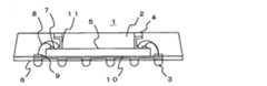
図1に、本実施形態にかかるLSIパッケージの外観を示す。BGA型LSIパッケージ1は、樹脂2で封止されており、その裏面(底面)にはプリント基板と接合するための外部電極端子3が複数設けられている。また、BGA型LSIパッケージ1の表面(上面)には、内部信号観測用の外部電極端子4が複数設けられている。[First Embodiment]
A first embodiment in which the present invention is suitably implemented will be described.
FIG. 1 shows the appearance of the LSI package according to the present embodiment. The BGA
図2に、BGA型LSIパッケージ1の縦断面(底面と垂直方向の断面)を示す。図示するのは図1のa−b線での断面である。また、図3に、BGA型LSIパッケージ1の横断面(底面と平行な方向の断面)を示す。図示するのは図1のc−d線での断面である。 FIG. 2 shows a longitudinal section (a section perpendicular to the bottom surface) of the BGA
半導体チップ5は、CPU、ASIC、メモリなどで構成されており、基板6上に設置される。 The
半導体チップ5上の複数の電極端子7の一部(7b)は、各々ワイヤ8を一本ずつ介して基板6の上の複数個の電極端子9のいずれかと電気的に接続されている。電極端子9は、基板6に形成された内部配線10を介して外部電極端子3と電気的に接続されている。 A part (7b) of the plurality of
これとは別に、半導体チップ5上の電極端子7の残りの一部(7a)は、各々ワイヤ8を一本ずつ介して側面視略コの字形のリードフレーム11のいずれかに接続され、これを介して外部電極端子4と電気的に接続されている。 Apart from this, the remaining part (7a) of the
リードフレーム11は、帯状部材の上端部及び下端部が基板6と略平行に折り曲げられた側面視略コの字形状であるが、BGA型LSIパッケージ1の製造過程においては上端部は基板6と垂直な状態(すなわち、側面視略L字形状)であり、下端部の上面にワイヤ8をボンディングした後で上端部を基板6と略平行に折り曲げることによって略コの字状に成型される。これにより、ワイヤ8のボンディングのしやすさと、外部電極端子4の面積の確保とを両立させている。 The lead frame 11 has a substantially U-shape in a side view in which the upper end portion and the lower end portion of the belt-like member are bent substantially in parallel with the
外部電極端子3,4、電極端子7,9、ワイヤ8、内部配線10、及びリードフレーム11はいずれも導体で形成されている。 The
図4に、BGA型LSIパッケージ1の機能構成を示す。半導体チップ5の内部には二つの機能ブロック(第1の機能部102、第2の機能部103)が構成されている。第1の機能部102は、半導体チップ5の外部へ信号104を出力し、半導体チップ5の外部から信号105が入力される。第2の機能部103は、半導体チップ5の外部から信号108が入力され、半導体チップ5の外部へ信号109を出力する。
信号104及び109は、外部電極端子3を介して半導体チップ5の外部へ出力される。また、信号105及び108は、外部電極端子3のいずれかを介して半導体チップ5の内部へ入力される。FIG. 4 shows a functional configuration of the BGA
The
内部信号106,107は、第1の機能部102から第2の機能部103へ、又は第2の機能部103から第1の機能部102へ出力される信号であり、半導体チップ5の外部へ出力しなくても機能上問題の無い信号である。ただし、外部電極端子3から出力される信号105又は108が正常でない場合に、第1の機能部102に原因があるのか第2の機能部103に原因があるのかを切り分けるために半導体チップ5の外部へ出力することは非常に効果的である。 The
BGA型LSIパッケージ1は、内部信号106,107を外部電極端子4から出力する。外部電極端子4は、樹脂2の上面に設けられているため、BGA型LSIパッケージ1に、観測したい内部信号の数ぶんの外部電極端子3を増やす必要はない。よって、外部電極端子3の増加に伴ってBGA型LSIパッケージ1の底面積が大きくなることはない。 The BGA
また、図5に示すように、外部電極端子4を用いてBGA型LSIパッケージ1の内部信号106,107の信号波形を直接プローブで測定できるため、プリント基板に検査用のランドを設ける従来の手法と比較して、より正確に信号波形を観測できる。 Further, as shown in FIG. 5, since the signal waveforms of the
本実施形態にかかるBGA型LSIパッケージ1の製造方法について説明する。基板6に半導体チップ5を実装し、半導体チップ5と電極端子9とをワイヤ8でボンディングするまでの工程は、従来のBGA型LSIパッケージの製造工程と同様である。図10に、半導体チップ5と電極端子9とをワイヤ8でボンディングした後の状態を示す。 A method for manufacturing the BGA
図11に、基板6にリードフレーム11を実装し、半導体チップ5の上面の外部電極端子4とワイヤ8を介して接続した状態を示す。リードフレーム11は、この段階(基板6に実装する段階)ではまだコの字形に成型されておらず、略L字形である。
半導体チップ5とリードフレーム11の下端部の上面とをワイヤ8を介して電気的に接続することによって、半導体チップ5とリードフレーム11とを電気的に接続するための配線を基板6に設ける必要が無くなる。半導体チップ5の内部信号を外部へ出力できるようにするために必要となるのは、リードフレーム11を実装するスペースのみであるから、半導体チップ5の内部信号を外部へ出力できる構成としても基板6の面積はほとんど増加しない。FIG. 11 shows a state in which the lead frame 11 is mounted on the
It is necessary to provide wiring on the
リードフレーム11は、ワイヤ8をボンディングする段階では略L字状であるため、ボンディング作業の妨げとはならない。 Since the lead frame 11 is substantially L-shaped when the
ワイヤ8のボンディングが完了した後、リードフレーム11の上端側が所定長さだけ突出するように樹脂2で封止する。その後、図12に示すように、リードフレーム11の上端側を基板6と略平行に折り曲げて側面視略コの字形状とする。 After the bonding of the
リードフレーム11の上端部を折り曲げた後、折り曲げた部分を除いてさらに樹脂2で封止する。これにより、リードフレーム11の上端部が折り曲げられた部分の上に凹部が形成される。図13に示すように、この凹部にははんだボールが設置される。設置されたはんだボールは樹脂2と同じ高さとなるように上面が切断され、BGA型LSIパッケージ1が完成する。 After the upper end portion of the lead frame 11 is bent, the lead frame 11 is further sealed with the
上記工程を経て形成したBGA型LSIパッケージ1は、上面が平坦であるため、図14に示すように、外部電極端子4の上に絶縁層(絶縁塗料や絶縁シール)を形成することによって、外部電極端子4を容易に絶縁できる。これにより、内部信号をBGA型LSIパッケージ1の外部に出力する必要がないときに、外部電極端子4からパッケージ内にノイズが侵入する恐れが無い。 Since the BGA
本実施形態にかかるBGA型LSIパッケージ1は、プリント基板に実装したあとでも外部電極端子4に測定器のプローブを接触させられるため、半導体チップ5に不具合が生じた場合などに、外部電極端子4を用いて内部信号の信号波形を容易かつ正確に観測できる。 In the BGA
しかも、BGA型であるにもかかわらず、プリント基板に検査用のランドパターンを設けておかなくても半導体チップ5の内部信号を観測可能である。 Moreover, the internal signal of the
なお、ここではリードフレーム11を略コの字状に成型する場合を例としたが、リードフレームの上端部を下端部とは逆方向に折り曲げてクランク形状としても良いことは言うまでもない。 In this example, the lead frame 11 is molded into a substantially U shape, but it goes without saying that the upper end portion of the lead frame may be bent in a direction opposite to the lower end portion to form a crank shape.
〔第2の実施形態〕
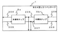
本発明を好適に実施した第2の実施形態について説明する。図6に、本実施形態にかかるBGA型LSIパッケージの構成を示す。BGA型LSIパッケージ1は、半導体チップを二つ(5a、5b)備える他は、第1の実施形態のBGA型LSIパッケージ1と同様の構成である。[Second Embodiment]
A second embodiment in which the present invention is suitably implemented will be described. FIG. 6 shows the configuration of the BGA type LSI package according to this embodiment. The BGA
図7に、本実施形態にかかるBGA型LSIパッケージ1の機能構成を示す。半導体チップ5a、5bは、それぞれ内部に一つの機能ブロックが構成されるものとする。
半導体チップ5aは、BGA型LSIパッケージ1の外部へ信号204を出力し、BGA型LSIパッケージ1の外部から信号205が入力される。半導体チップ5bは、BGA型LSIパッケージ1の外部から信号208が入力され、BGA型LSIパッケージ1の外部へ信号209を出力する。
信号204及び209は、外部電極端子3を介してBGA型LSIパッケージ1の外部へ出力される。また、信号205及び208は、外部電極端子3のいずれかを介してBGA型LSIパッケージ1の内部へ入力される。FIG. 7 shows a functional configuration of the BGA
The semiconductor chip 5a outputs a
The
内部信号206,207は、半導体チップ5aから半導体チップ5bへ、又は半導体チップ5bから半導体チップ5aへ出力される信号であり、BGA型LSIパッケージ1の外部へ出力しなくても機能上問題の無い信号である。ただし、外部電極端子3から出力される信号205又は208が正常でない場合に、半導体チップ5aに原因があるのか半導体チップ5bに原因があるのかを切り分けるためにBGA型LSIパッケージ1の外部へ出力することは非常に効果的である。 The
BGA型LSIパッケージ1は、内部信号206,207を外部電極端子4から出力する。外部電極端子4は、樹脂2の上面に設けられているため、BGA型LSIパッケージ1に、観測したい内部信号の数ぶんの外部電極端子3を増やす必要はない。よって、外部電極端子3の増加に伴ってBGA型LSIパッケージ1の底面積が大きくなることはない。 The BGA
また、第1の実施形態と同様に、外部電極端子4を用いてBGA型LSIパッケージ1の内部信号206,207の信号波形を直接プローブで測定できるため、プリント基板に検査用のランドを設ける従来の手法よりもより正確に信号波形を観測できる。 Similarly to the first embodiment, since the signal waveforms of the
本実施形態にかかるBGA型LSIパッケージ1は、プリント基板に実装したあとでも外部電極端子4に測定器のプローブを接触させられるため、半導体チップ5a、5bに不具合が生じた場合などに、外部電極端子4を用いて内部信号の信号波形を容易かつ正確に観測できる。 In the BGA
本実施形態においては、半導体チップ5a及び5bのそれぞれを一つの機能ブロックと見なす場合を例として説明したが、第1の実施形態と同様に半導体チップ5aや5b内に複数の機能ブロックが形成されていても良い。
また、本実施形態においては、半導体チップ5a及び5bを積層させて配置した構成を例としたが、基板6上に複数の半導体チップ5を配列させることも可能である。In the present embodiment, the case where each of the
In the present embodiment, the
〔第3の実施形態〕
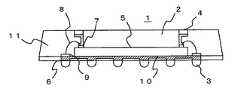
本発明を好適に実施した第3の実施形態について説明する。
図15に、本実施形態にかかるBGA型LSIパッケージの縦断面を示す。図16に、本実施形態にかかるBGA型LSIパッケージ1の横断面を示す。
本実施形態にかかるBGA型LSIパッケージ1は、第1の実施形態とほぼ同様の構成であるが、リードフレーム11は、基板6上ではなく半導体チップ5上に設置されている。外部電極端子4とリードフレーム8とはワイヤ8を介して電気的に接続されている。[Third Embodiment]
A third embodiment in which the present invention is preferably implemented will be described.
FIG. 15 shows a longitudinal section of the BGA type LSI package according to the present embodiment. FIG. 16 shows a cross section of the BGA
The BGA
本実施形態にかかるBGA型LSIパッケージ1は、基板6の上にはリードフレーム11を設置するためのスペースをも設ける必要がないため、従来のBGA型LSIパッケージと比較して基板6の面積は全く増加していない。 Since the BGA
しかも、上記第1の実施形態と同様に、BGA型であるにもかかわらず、プリント基板に検査用のランドパターンを設けなくても半導体チップ5の内部信号を観測可能である。 In addition, as in the first embodiment, the internal signal of the
〔第4の実施形態〕
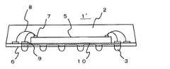
本発明を好適に実施した第4の実施形態について説明する。
図17に、本実施形態にかかるBGA型LSIパッケージ1の縦断面を示す。図18に、本実施形態にかかるBGA型LSIパッケージの横断面を示す。
本実施形態にかかるBGA型LSIパッケージ1は、第1の実施形態とほぼ同様の構成であるが、リードフレーム11は、基板6の上ではなく半導体チップ5上に設置されている。外部電極端子4とリードフレーム11とはワイヤ8を介することなく電気的に接続されている。[Fourth Embodiment]
A fourth embodiment in which the present invention is preferably implemented will be described.
FIG. 17 shows a longitudinal section of the BGA
The BGA
本実施形態にかかるBGA型LSIパッケージ1は、第3の実施形態と同様の効果が得られる。しかも、外部電極端子4とリードフレーム11とをワイヤボンディングする必要がないため、製造がより容易である。すなわち、ワイヤボンディングの手間を軽減できるのみならず、リードフレームの上端部を折り曲げる必要もない。よって、リードフレーム11を最初から略コの字形状にしておいて半導体チップ5の上に設置しても良いし、側面視略工の字形状などとすることも可能である。 The BGA
なお、上記各実施形態は本発明の好適な実施の一例であり、本発明はこれらに限定されることはない。
例えば、上記各実施形態においては、BGA型のLSIパッケージを例として説明したが、FQP型のLSIパッケージの上面に外部電極端子を設け、ここから内部信号を出力可能としても良い。この場合にも、内部信号の信号波形を容易かつ正確に観測できるという効果が得られる。
また、上記各実施形態においては、全てのリードフレームを基板又は半導体チップの上に設置する構成を例としたが、一部のリードフレームを基板上に設置し、残りの一部を半導体チップ上に設置するようにしても良い。
このように、本発明は様々な変形が可能である。Each of the above embodiments is an example of a preferred embodiment of the present invention, and the present invention is not limited to these.
For example, in each of the above embodiments, the BGA type LSI package has been described as an example. However, an external electrode terminal may be provided on the upper surface of the FQP type LSI package so that an internal signal can be output therefrom. Also in this case, the effect that the signal waveform of the internal signal can be observed easily and accurately is obtained.
Further, in each of the above embodiments, the configuration in which all the lead frames are installed on the substrate or the semiconductor chip is taken as an example. However, a part of the lead frames is installed on the substrate and the remaining part is placed on the semiconductor chip. You may make it install in.
As described above, the present invention can be variously modified.
1 BGA型LSIパッケージ
2 樹脂
3、4 外部電極端子
5、5a、5b 半導体チップ
6 基板
7、9 電極端子
8 ワイヤ
10 内部配線
11 リードフレームDESCRIPTION OF
Claims (9)
Translated fromJapanese前記半導体チップは、内部信号を出力するため、又は該内部信号を出力するために必要な信号を入力するための第1の内部電極端子と、半導体チップとしての機能を実現するための動作信号を出力するため、又は該動作信号を出力するために必要な信号を入力するための第2の内部電極端子とを前記基板との接合面とは異なる面に備え、
前記第1の内部電極端子は、前記基板上に設置された導電性部材と該基板内部の配線を介することなく電気的に接続されており、
前記第2の内部電極端子は、前記基板上に設置された基板電極端子とワイヤを介して接続され、前記基板に設けられた外部電極端子とは該基板内部の配線を介して電気的に接続されており、
前記導電性部材は、前記樹脂を貫通しており、上端部には内部検査用電極端子が設けられていることを特徴とする半導体装置。A semiconductor device in which a surface on which a semiconductor chip is mounted on a surface on which a semiconductor chip is mounted is sealed with resin.
The semiconductor chip outputs a first internal electrode terminal for inputting an internal signal or inputting a signal necessary for outputting the internal signal, and an operation signal for realizing a function as the semiconductor chip. A second internal electrode terminal for inputting a signal necessary for outputting or outputting the operation signal is provided on a surface different from a bonding surface with the substrate,
The first internal electrode terminal is electrically connected to the conductive member installed on the substrate without going through the wiring inside the substrate,
The second internal electrode terminal is connected to a substrate electrode terminal installed on the substrate via a wire, and is electrically connected to an external electrode terminal provided on the substrate via a wiring inside the substrate. Has been
The semiconductor device according to claim 1, wherein the conductive member penetrates the resin, and an upper end portion is provided with an internal inspection electrode terminal.
前記半導体チップは、内部信号を出力するため、又は該内部信号を出力するために必要な信号を入力するための第1の内部電極端子と、半導体チップとしての機能を実現するための動作信号を出力するため、又は該動作信号を出力するために必要な信号を入力するための第2の内部電極端子とを前記基板との接合面とは異なる面に備え、
前記第1の内部電極端子は、前記半導体チップ上に設置された導電性部材と前記基板を介することなく電気的に接続されており、
前記第2の内部電極端子は、前記基板上に設置された基板電極端子とワイヤを介して接続され、前記基板に設けられた外部電極端子とは該基板内部の配線を介して電気的に接続されており、
前記導電性部材は、前記樹脂を貫通しており、上端部には内部検査用電極端子が設けられていることを特徴とする半導体装置。A semiconductor device in which a surface on which a semiconductor chip is mounted on a surface on which a semiconductor chip is mounted is sealed with resin.
The semiconductor chip outputs a first internal electrode terminal for inputting an internal signal or a signal necessary for outputting the internal signal, and an operation signal for realizing a function as a semiconductor chip. A second internal electrode terminal for inputting a signal necessary for outputting or outputting the operation signal is provided on a surface different from a bonding surface with the substrate,
The first internal electrode terminal is electrically connected to the conductive member installed on the semiconductor chip without passing through the substrate,
The second internal electrode terminal is connected to a substrate electrode terminal installed on the substrate via a wire, and is electrically connected to an external electrode terminal provided on the substrate via a wiring inside the substrate. Has been
The semiconductor device according to claim 1, wherein the conductive member penetrates the resin, and an upper end portion is provided with an internal inspection electrode terminal.
Priority Applications (1)
| Application Number | Priority Date | Filing Date | Title |
|---|---|---|---|
| JP2006054362AJP2007234845A (en) | 2006-03-01 | 2006-03-01 | Semiconductor device |
Applications Claiming Priority (1)
| Application Number | Priority Date | Filing Date | Title |
|---|---|---|---|
| JP2006054362AJP2007234845A (en) | 2006-03-01 | 2006-03-01 | Semiconductor device |
Publications (1)
| Publication Number | Publication Date |
|---|---|
| JP2007234845Atrue JP2007234845A (en) | 2007-09-13 |
Family
ID=38555128
Family Applications (1)
| Application Number | Title | Priority Date | Filing Date |
|---|---|---|---|
| JP2006054362AWithdrawnJP2007234845A (en) | 2006-03-01 | 2006-03-01 | Semiconductor device |
Country Status (1)
| Country | Link |
|---|---|
| JP (1) | JP2007234845A (en) |
Cited By (37)
| Publication number | Priority date | Publication date | Assignee | Title |
|---|---|---|---|---|
| JP2015508240A (en)* | 2012-02-24 | 2015-03-16 | インヴェンサス・コーポレイション | Method for package-on-package assembly having wire bonds to sealing surfaces |
| US9349706B2 (en) | 2012-02-24 | 2016-05-24 | Invensas Corporation | Method for package-on-package assembly with wire bonds to encapsulation surface |
| US9391008B2 (en) | 2012-07-31 | 2016-07-12 | Invensas Corporation | Reconstituted wafer-level package DRAM |
| US9412714B2 (en) | 2014-05-30 | 2016-08-09 | Invensas Corporation | Wire bond support structure and microelectronic package including wire bonds therefrom |
| US9502390B2 (en) | 2012-08-03 | 2016-11-22 | Invensas Corporation | BVA interposer |
| US9553076B2 (en) | 2010-07-19 | 2017-01-24 | Tessera, Inc. | Stackable molded microelectronic packages with area array unit connectors |
| US9570382B2 (en) | 2010-07-19 | 2017-02-14 | Tessera, Inc. | Stackable molded microelectronic packages |
| US9570416B2 (en) | 2004-11-03 | 2017-02-14 | Tessera, Inc. | Stacked packaging improvements |
| US9583411B2 (en) | 2014-01-17 | 2017-02-28 | Invensas Corporation | Fine pitch BVA using reconstituted wafer with area array accessible for testing |
| US9601454B2 (en) | 2013-02-01 | 2017-03-21 | Invensas Corporation | Method of forming a component having wire bonds and a stiffening layer |
| US9615456B2 (en) | 2012-12-20 | 2017-04-04 | Invensas Corporation | Microelectronic assembly for microelectronic packaging with bond elements to encapsulation surface |
| US9659848B1 (en) | 2015-11-18 | 2017-05-23 | Invensas Corporation | Stiffened wires for offset BVA |
| US9685365B2 (en) | 2013-08-08 | 2017-06-20 | Invensas Corporation | Method of forming a wire bond having a free end |
| US9691731B2 (en) | 2011-05-03 | 2017-06-27 | Tessera, Inc. | Package-on-package assembly with wire bonds to encapsulation surface |
| US9728527B2 (en) | 2013-11-22 | 2017-08-08 | Invensas Corporation | Multiple bond via arrays of different wire heights on a same substrate |
| US9735084B2 (en) | 2014-12-11 | 2017-08-15 | Invensas Corporation | Bond via array for thermal conductivity |
| US9761554B2 (en) | 2015-05-07 | 2017-09-12 | Invensas Corporation | Ball bonding metal wire bond wires to metal pads |
| US9761558B2 (en) | 2011-10-17 | 2017-09-12 | Invensas Corporation | Package-on-package assembly with wire bond vias |
| US9812402B2 (en) | 2015-10-12 | 2017-11-07 | Invensas Corporation | Wire bond wires for interference shielding |
| US9842745B2 (en) | 2012-02-17 | 2017-12-12 | Invensas Corporation | Heat spreading substrate with embedded interconnects |
| US9852969B2 (en) | 2013-11-22 | 2017-12-26 | Invensas Corporation | Die stacks with one or more bond via arrays of wire bond wires and with one or more arrays of bump interconnects |
| US9888579B2 (en) | 2015-03-05 | 2018-02-06 | Invensas Corporation | Pressing of wire bond wire tips to provide bent-over tips |
| US9911718B2 (en) | 2015-11-17 | 2018-03-06 | Invensas Corporation | ‘RDL-First’ packaged microelectronic device for a package-on-package device |
| US9935075B2 (en) | 2016-07-29 | 2018-04-03 | Invensas Corporation | Wire bonding method and apparatus for electromagnetic interference shielding |
| US9953914B2 (en) | 2012-05-22 | 2018-04-24 | Invensas Corporation | Substrate-less stackable package with wire-bond interconnect |
| US9984901B2 (en) | 2005-12-23 | 2018-05-29 | Tessera, Inc. | Method for making a microelectronic assembly having conductive elements |
| US9984992B2 (en) | 2015-12-30 | 2018-05-29 | Invensas Corporation | Embedded wire bond wires for vertical integration with separate surface mount and wire bond mounting surfaces |
| US10008477B2 (en) | 2013-09-16 | 2018-06-26 | Invensas Corporation | Microelectronic element with bond elements to encapsulation surface |
| US10008469B2 (en) | 2015-04-30 | 2018-06-26 | Invensas Corporation | Wafer-level packaging using wire bond wires in place of a redistribution layer |
| US10026717B2 (en) | 2013-11-22 | 2018-07-17 | Invensas Corporation | Multiple bond via arrays of different wire heights on a same substrate |
| US10181457B2 (en) | 2015-10-26 | 2019-01-15 | Invensas Corporation | Microelectronic package for wafer-level chip scale packaging with fan-out |
| US10299368B2 (en) | 2016-12-21 | 2019-05-21 | Invensas Corporation | Surface integrated waveguides and circuit structures therefor |
| US10332854B2 (en) | 2015-10-23 | 2019-06-25 | Invensas Corporation | Anchoring structure of fine pitch bva |
| US10381326B2 (en) | 2014-05-28 | 2019-08-13 | Invensas Corporation | Structure and method for integrated circuits packaging with increased density |
| US10460958B2 (en) | 2013-08-07 | 2019-10-29 | Invensas Corporation | Method of manufacturing embedded packaging with preformed vias |
| US10490528B2 (en) | 2015-10-12 | 2019-11-26 | Invensas Corporation | Embedded wire bond wires |
| CN113764361A (en)* | 2021-07-23 | 2021-12-07 | 上海闻泰信息技术有限公司 | Chip packaging structure and chip packaging method |
- 2006
- 2006-03-01JPJP2006054362Apatent/JP2007234845A/ennot_activeWithdrawn
Cited By (64)
| Publication number | Priority date | Publication date | Assignee | Title |
|---|---|---|---|---|
| US9570416B2 (en) | 2004-11-03 | 2017-02-14 | Tessera, Inc. | Stacked packaging improvements |
| US9984901B2 (en) | 2005-12-23 | 2018-05-29 | Tessera, Inc. | Method for making a microelectronic assembly having conductive elements |
| US10128216B2 (en) | 2010-07-19 | 2018-11-13 | Tessera, Inc. | Stackable molded microelectronic packages |
| US9553076B2 (en) | 2010-07-19 | 2017-01-24 | Tessera, Inc. | Stackable molded microelectronic packages with area array unit connectors |
| US9570382B2 (en) | 2010-07-19 | 2017-02-14 | Tessera, Inc. | Stackable molded microelectronic packages |
| US11424211B2 (en) | 2011-05-03 | 2022-08-23 | Tessera Llc | Package-on-package assembly with wire bonds to encapsulation surface |
| US10593643B2 (en) | 2011-05-03 | 2020-03-17 | Tessera, Inc. | Package-on-package assembly with wire bonds to encapsulation surface |
| US10062661B2 (en) | 2011-05-03 | 2018-08-28 | Tessera, Inc. | Package-on-package assembly with wire bonds to encapsulation surface |
| US9691731B2 (en) | 2011-05-03 | 2017-06-27 | Tessera, Inc. | Package-on-package assembly with wire bonds to encapsulation surface |
| US11189595B2 (en) | 2011-10-17 | 2021-11-30 | Invensas Corporation | Package-on-package assembly with wire bond vias |
| US11735563B2 (en) | 2011-10-17 | 2023-08-22 | Invensas Llc | Package-on-package assembly with wire bond vias |
| US10756049B2 (en) | 2011-10-17 | 2020-08-25 | Invensas Corporation | Package-on-package assembly with wire bond vias |
| US9761558B2 (en) | 2011-10-17 | 2017-09-12 | Invensas Corporation | Package-on-package assembly with wire bond vias |
| US9842745B2 (en) | 2012-02-17 | 2017-12-12 | Invensas Corporation | Heat spreading substrate with embedded interconnects |
| JP2015508240A (en)* | 2012-02-24 | 2015-03-16 | インヴェンサス・コーポレイション | Method for package-on-package assembly having wire bonds to sealing surfaces |
| US9349706B2 (en) | 2012-02-24 | 2016-05-24 | Invensas Corporation | Method for package-on-package assembly with wire bonds to encapsulation surface |
| US9691679B2 (en) | 2012-02-24 | 2017-06-27 | Invensas Corporation | Method for package-on-package assembly with wire bonds to encapsulation surface |
| US10170412B2 (en) | 2012-05-22 | 2019-01-01 | Invensas Corporation | Substrate-less stackable package with wire-bond interconnect |
| US9953914B2 (en) | 2012-05-22 | 2018-04-24 | Invensas Corporation | Substrate-less stackable package with wire-bond interconnect |
| US10510659B2 (en) | 2012-05-22 | 2019-12-17 | Invensas Corporation | Substrate-less stackable package with wire-bond interconnect |
| US9391008B2 (en) | 2012-07-31 | 2016-07-12 | Invensas Corporation | Reconstituted wafer-level package DRAM |
| US9917073B2 (en) | 2012-07-31 | 2018-03-13 | Invensas Corporation | Reconstituted wafer-level package dram with conductive interconnects formed in encapsulant at periphery of the package |
| US9502390B2 (en) | 2012-08-03 | 2016-11-22 | Invensas Corporation | BVA interposer |
| US10297582B2 (en) | 2012-08-03 | 2019-05-21 | Invensas Corporation | BVA interposer |
| US9615456B2 (en) | 2012-12-20 | 2017-04-04 | Invensas Corporation | Microelectronic assembly for microelectronic packaging with bond elements to encapsulation surface |
| US9601454B2 (en) | 2013-02-01 | 2017-03-21 | Invensas Corporation | Method of forming a component having wire bonds and a stiffening layer |
| US10460958B2 (en) | 2013-08-07 | 2019-10-29 | Invensas Corporation | Method of manufacturing embedded packaging with preformed vias |
| US9685365B2 (en) | 2013-08-08 | 2017-06-20 | Invensas Corporation | Method of forming a wire bond having a free end |
| US10008477B2 (en) | 2013-09-16 | 2018-06-26 | Invensas Corporation | Microelectronic element with bond elements to encapsulation surface |
| US9852969B2 (en) | 2013-11-22 | 2017-12-26 | Invensas Corporation | Die stacks with one or more bond via arrays of wire bond wires and with one or more arrays of bump interconnects |
| USRE49987E1 (en) | 2013-11-22 | 2024-05-28 | Invensas Llc | Multiple plated via arrays of different wire heights on a same substrate |
| US10629567B2 (en) | 2013-11-22 | 2020-04-21 | Invensas Corporation | Multiple plated via arrays of different wire heights on same substrate |
| US9728527B2 (en) | 2013-11-22 | 2017-08-08 | Invensas Corporation | Multiple bond via arrays of different wire heights on a same substrate |
| US10290613B2 (en) | 2013-11-22 | 2019-05-14 | Invensas Corporation | Multiple bond via arrays of different wire heights on a same substrate |
| US10026717B2 (en) | 2013-11-22 | 2018-07-17 | Invensas Corporation | Multiple bond via arrays of different wire heights on a same substrate |
| US10529636B2 (en) | 2014-01-17 | 2020-01-07 | Invensas Corporation | Fine pitch BVA using reconstituted wafer with area array accessible for testing |
| US9583411B2 (en) | 2014-01-17 | 2017-02-28 | Invensas Corporation | Fine pitch BVA using reconstituted wafer with area array accessible for testing |
| US9837330B2 (en) | 2014-01-17 | 2017-12-05 | Invensas Corporation | Fine pitch BVA using reconstituted wafer with area array accessible for testing |
| US11404338B2 (en) | 2014-01-17 | 2022-08-02 | Invensas Corporation | Fine pitch bva using reconstituted wafer with area array accessible for testing |
| US11990382B2 (en) | 2014-01-17 | 2024-05-21 | Adeia Semiconductor Technologies Llc | Fine pitch BVA using reconstituted wafer with area array accessible for testing |
| US10381326B2 (en) | 2014-05-28 | 2019-08-13 | Invensas Corporation | Structure and method for integrated circuits packaging with increased density |
| US9947641B2 (en) | 2014-05-30 | 2018-04-17 | Invensas Corporation | Wire bond support structure and microelectronic package including wire bonds therefrom |
| US9412714B2 (en) | 2014-05-30 | 2016-08-09 | Invensas Corporation | Wire bond support structure and microelectronic package including wire bonds therefrom |
| US9735084B2 (en) | 2014-12-11 | 2017-08-15 | Invensas Corporation | Bond via array for thermal conductivity |
| US10806036B2 (en) | 2015-03-05 | 2020-10-13 | Invensas Corporation | Pressing of wire bond wire tips to provide bent-over tips |
| US9888579B2 (en) | 2015-03-05 | 2018-02-06 | Invensas Corporation | Pressing of wire bond wire tips to provide bent-over tips |
| US10008469B2 (en) | 2015-04-30 | 2018-06-26 | Invensas Corporation | Wafer-level packaging using wire bond wires in place of a redistribution layer |
| US9761554B2 (en) | 2015-05-07 | 2017-09-12 | Invensas Corporation | Ball bonding metal wire bond wires to metal pads |
| US10490528B2 (en) | 2015-10-12 | 2019-11-26 | Invensas Corporation | Embedded wire bond wires |
| US11462483B2 (en) | 2015-10-12 | 2022-10-04 | Invensas Llc | Wire bond wires for interference shielding |
| US10115678B2 (en) | 2015-10-12 | 2018-10-30 | Invensas Corporation | Wire bond wires for interference shielding |
| US10559537B2 (en) | 2015-10-12 | 2020-02-11 | Invensas Corporation | Wire bond wires for interference shielding |
| US9812402B2 (en) | 2015-10-12 | 2017-11-07 | Invensas Corporation | Wire bond wires for interference shielding |
| US10332854B2 (en) | 2015-10-23 | 2019-06-25 | Invensas Corporation | Anchoring structure of fine pitch bva |
| US10181457B2 (en) | 2015-10-26 | 2019-01-15 | Invensas Corporation | Microelectronic package for wafer-level chip scale packaging with fan-out |
| US10043779B2 (en) | 2015-11-17 | 2018-08-07 | Invensas Corporation | Packaged microelectronic device for a package-on-package device |
| US9911718B2 (en) | 2015-11-17 | 2018-03-06 | Invensas Corporation | ‘RDL-First’ packaged microelectronic device for a package-on-package device |
| US9659848B1 (en) | 2015-11-18 | 2017-05-23 | Invensas Corporation | Stiffened wires for offset BVA |
| US10325877B2 (en) | 2015-12-30 | 2019-06-18 | Invensas Corporation | Embedded wire bond wires for vertical integration with separate surface mount and wire bond mounting surfaces |
| US9984992B2 (en) | 2015-12-30 | 2018-05-29 | Invensas Corporation | Embedded wire bond wires for vertical integration with separate surface mount and wire bond mounting surfaces |
| US10658302B2 (en) | 2016-07-29 | 2020-05-19 | Invensas Corporation | Wire bonding method and apparatus for electromagnetic interference shielding |
| US9935075B2 (en) | 2016-07-29 | 2018-04-03 | Invensas Corporation | Wire bonding method and apparatus for electromagnetic interference shielding |
| US10299368B2 (en) | 2016-12-21 | 2019-05-21 | Invensas Corporation | Surface integrated waveguides and circuit structures therefor |
| CN113764361A (en)* | 2021-07-23 | 2021-12-07 | 上海闻泰信息技术有限公司 | Chip packaging structure and chip packaging method |
Similar Documents
| Publication | Publication Date | Title |
|---|---|---|
| JP2007234845A (en) | Semiconductor device | |
| US10459007B2 (en) | Probe card | |
| JP4252491B2 (en) | Module with inspection function and inspection method thereof. | |
| US20070120237A1 (en) | Semiconductor integrated circuit | |
| KR20010080509A (en) | Integrated circuit chip, integrated circuit, printed-circuit board and electronic device | |
| JP2000088921A (en) | Semiconductor device | |
| JP5131812B2 (en) | Semiconductor device | |
| JP2004063616A (en) | Lead frame, manufacturing method of semiconductor device using the same and electric characteristic inspecting method of small-sized element | |
| JPH1117058A (en) | Bga package, test socket therefor and test for bga package | |
| US20060091535A1 (en) | Fine pitch bonding pad layout and method of manufacturing same | |
| KR100723518B1 (en) | Interposer pattern with pad chain | |
| US6433565B1 (en) | Test fixture for flip chip ball grid array circuits | |
| JP2009130217A (en) | Semiconductor device and method of manufacturing the same | |
| KR100258350B1 (en) | Super bga semiconductor package | |
| JP2885202B2 (en) | Inspection jig for semiconductor package | |
| JP2901518B2 (en) | Multi-chip semiconductor device | |
| JP2006278374A (en) | Semiconductor device and packaging structure thereof | |
| JPH03228356A (en) | Ic package | |
| JP4056252B2 (en) | Manufacturing method of semiconductor device | |
| JP4701445B2 (en) | Semiconductor package | |
| JP2924847B2 (en) | Semiconductor package | |
| JPH1117057A (en) | Bga type semiconductor device with inspection pads | |
| JP2007214454A (en) | Unit for substrate connection test | |
| JP2010062469A (en) | Semiconductor module | |
| US20060028228A1 (en) | Test pads for IC chip |
Legal Events
| Date | Code | Title | Description |
|---|---|---|---|
| A300 | Withdrawal of application because of no request for examination | Free format text:JAPANESE INTERMEDIATE CODE: A300 Effective date:20090512 |