JP2007234001A - Semiconductor device - Google Patents
Semiconductor deviceDownload PDFInfo
- Publication number
- JP2007234001A JP2007234001AJP2007020267AJP2007020267AJP2007234001AJP 2007234001 AJP2007234001 AJP 2007234001AJP 2007020267 AJP2007020267 AJP 2007020267AJP 2007020267 AJP2007020267 AJP 2007020267AJP 2007234001 AJP2007234001 AJP 2007234001A
- Authority
- JP
- Japan
- Prior art keywords
- circuit
- chip
- side channel
- program
- memory
- Prior art date
- Legal status (The legal status is an assumption and is not a legal conclusion. Google has not performed a legal analysis and makes no representation as to the accuracy of the status listed.)
- Withdrawn
Links
- 239000004065semiconductorSubstances0.000titleclaimsdescription72
- 238000012545processingMethods0.000claimsabstractdescription35
- 238000000034methodMethods0.000claimsdescription82
- 238000006243chemical reactionMethods0.000claimsdescription33
- 230000008569processEffects0.000claimsdescription27
- 230000005540biological transmissionEffects0.000claimsdescription26
- 230000009466transformationEffects0.000claimsdescription23
- 238000004364calculation methodMethods0.000claimsdescription11
- 238000000605extractionMethods0.000claimsdescription10
- 230000008054signal transmissionEffects0.000claimsdescription4
- 125000004122cyclic groupChemical group0.000claimsdescription3
- 238000004458analytical methodMethods0.000abstractdescription13
- 230000005855radiationEffects0.000abstractdescription5
- 230000000903blocking effectEffects0.000abstract1
- 239000010410layerSubstances0.000description102
- 230000006870functionEffects0.000description85
- 239000010408filmSubstances0.000description80
- 239000000758substrateSubstances0.000description47
- 230000008859changeEffects0.000description44
- XUIMIQQOPSSXEZ-UHFFFAOYSA-NSiliconChemical compound[Si]XUIMIQQOPSSXEZ-UHFFFAOYSA-N0.000description43
- 229910052710siliconInorganic materials0.000description43
- 239000010703siliconSubstances0.000description43
- 239000012535impuritySubstances0.000description29
- 238000004519manufacturing processMethods0.000description29
- 230000002441reversible effectEffects0.000description26
- 230000002265preventionEffects0.000description25
- 238000013461designMethods0.000description21
- 238000010438heat treatmentMethods0.000description15
- 239000000463materialSubstances0.000description15
- 239000011229interlayerSubstances0.000description14
- 230000015572biosynthetic processEffects0.000description13
- 238000004891communicationMethods0.000description13
- 238000010586diagramMethods0.000description13
- 230000007547defectEffects0.000description12
- 238000005530etchingMethods0.000description11
- 230000006872improvementEffects0.000description11
- 239000010936titaniumSubstances0.000description11
- 229910052751metalInorganic materials0.000description10
- 239000002184metalSubstances0.000description10
- 230000001681protective effectEffects0.000description10
- PXHVJJICTQNCMI-UHFFFAOYSA-NNickelChemical compound[Ni]PXHVJJICTQNCMI-UHFFFAOYSA-N0.000description9
- 239000013078crystalSubstances0.000description9
- 239000011347resinSubstances0.000description9
- 229920005989resinPolymers0.000description9
- 238000001312dry etchingMethods0.000description8
- 238000005247getteringMethods0.000description8
- 229910052581Si3N4Inorganic materials0.000description7
- 238000007726management methodMethods0.000description7
- 230000007246mechanismEffects0.000description7
- 229910021420polycrystalline siliconInorganic materials0.000description7
- VYPSYNLAJGMNEJ-UHFFFAOYSA-Nsilicon dioxideInorganic materialsO=[Si]=OVYPSYNLAJGMNEJ-UHFFFAOYSA-N0.000description7
- HQVNEWCFYHHQES-UHFFFAOYSA-Nsilicon nitrideChemical compoundN12[Si]34N5[Si]62N3[Si]51N64HQVNEWCFYHHQES-UHFFFAOYSA-N0.000description7
- KRHYYFGTRYWZRS-UHFFFAOYSA-NFluoraneChemical compoundFKRHYYFGTRYWZRS-UHFFFAOYSA-N0.000description6
- KDLHZDBZIXYQEI-UHFFFAOYSA-NPalladiumChemical compound[Pd]KDLHZDBZIXYQEI-UHFFFAOYSA-N0.000description6
- OAICVXFJPJFONN-UHFFFAOYSA-NPhosphorusChemical compound[P]OAICVXFJPJFONN-UHFFFAOYSA-N0.000description6
- RTAQQCXQSZGOHL-UHFFFAOYSA-NTitaniumChemical compound[Ti]RTAQQCXQSZGOHL-UHFFFAOYSA-N0.000description6
- 239000011521glassSubstances0.000description6
- 229910052739hydrogenInorganic materials0.000description6
- 229910052760oxygenInorganic materials0.000description6
- 229910052698phosphorusInorganic materials0.000description6
- 239000011574phosphorusSubstances0.000description6
- 229910052814silicon oxideInorganic materials0.000description6
- 229910052719titaniumInorganic materials0.000description6
- 229910052721tungstenInorganic materials0.000description6
- 239000010937tungstenSubstances0.000description6
- 238000001039wet etchingMethods0.000description6
- MHAJPDPJQMAIIY-UHFFFAOYSA-NHydrogen peroxideChemical compoundOOMHAJPDPJQMAIIY-UHFFFAOYSA-N0.000description5
- 239000000956alloySubstances0.000description5
- 229910052782aluminiumInorganic materials0.000description5
- XAGFODPZIPBFFR-UHFFFAOYSA-NaluminiumChemical compound[Al]XAGFODPZIPBFFR-UHFFFAOYSA-N0.000description5
- QVGXLLKOCUKJST-UHFFFAOYSA-Natomic oxygenChemical compound[O]QVGXLLKOCUKJST-UHFFFAOYSA-N0.000description5
- 239000000919ceramicSubstances0.000description5
- 238000002425crystallisationMethods0.000description5
- 230000008025crystallizationEffects0.000description5
- 238000013478data encryption standardMethods0.000description5
- 239000001257hydrogenSubstances0.000description5
- 239000001301oxygenSubstances0.000description5
- 238000005268plasma chemical vapour depositionMethods0.000description5
- 229920005591polysiliconPolymers0.000description5
- 229910021332silicideInorganic materials0.000description5
- FVBUAEGBCNSCDD-UHFFFAOYSA-Nsilicide(4-)Chemical compound[Si-4]FVBUAEGBCNSCDD-UHFFFAOYSA-N0.000description5
- 239000002356single layerSubstances0.000description5
- WFKWXMTUELFFGS-UHFFFAOYSA-NtungstenChemical compound[W]WFKWXMTUELFFGS-UHFFFAOYSA-N0.000description5
- ZOXJGFHDIHLPTG-UHFFFAOYSA-NBoronChemical compound[B]ZOXJGFHDIHLPTG-UHFFFAOYSA-N0.000description4
- UFHFLCQGNIYNRP-UHFFFAOYSA-NHydrogenChemical compound[H][H]UFHFLCQGNIYNRP-UHFFFAOYSA-N0.000description4
- 229910045601alloyInorganic materials0.000description4
- 229910052796boronInorganic materials0.000description4
- 239000003990capacitorSubstances0.000description4
- 239000003795chemical substances by applicationSubstances0.000description4
- 238000005229chemical vapour depositionMethods0.000description4
- 230000005672electromagnetic fieldEffects0.000description4
- 238000010894electron beam technologyMethods0.000description4
- 229910010272inorganic materialInorganic materials0.000description4
- 239000011147inorganic materialSubstances0.000description4
- 239000011810insulating materialSubstances0.000description4
- 238000005468ion implantationMethods0.000description4
- 238000002955isolationMethods0.000description4
- 239000011159matrix materialSubstances0.000description4
- 239000011259mixed solutionSubstances0.000description4
- 239000011368organic materialSubstances0.000description4
- 238000002161passivationMethods0.000description4
- 239000010948rhodiumSubstances0.000description4
- 229910052715tantalumInorganic materials0.000description4
- GUVRBAGPIYLISA-UHFFFAOYSA-Ntantalum atomChemical compound[Ta]GUVRBAGPIYLISA-UHFFFAOYSA-N0.000description4
- QTBSBXVTEAMEQO-UHFFFAOYSA-NAcetic acidChemical compoundCC(O)=OQTBSBXVTEAMEQO-UHFFFAOYSA-N0.000description3
- ZOKXTWBITQBERF-UHFFFAOYSA-NMolybdenumChemical compound[Mo]ZOKXTWBITQBERF-UHFFFAOYSA-N0.000description3
- 239000004642PolyimideSubstances0.000description3
- 238000001994activationMethods0.000description3
- UMIVXZPTRXBADB-UHFFFAOYSA-NbenzocyclobuteneChemical compoundC1=CC=C2CCC2=C1UMIVXZPTRXBADB-UHFFFAOYSA-N0.000description3
- 239000010949copperSubstances0.000description3
- 239000003989dielectric materialSubstances0.000description3
- 230000000694effectsEffects0.000description3
- -1for exampleSubstances0.000description3
- 239000007789gasSubstances0.000description3
- 230000001678irradiating effectEffects0.000description3
- 239000000203mixtureSubstances0.000description3
- 229910052750molybdenumInorganic materials0.000description3
- 239000011733molybdenumSubstances0.000description3
- 229910052759nickelInorganic materials0.000description3
- 150000004767nitridesChemical class0.000description3
- 238000000206photolithographyMethods0.000description3
- BASFCYQUMIYNBI-UHFFFAOYSA-NplatinumChemical compound[Pt]BASFCYQUMIYNBI-UHFFFAOYSA-N0.000description3
- 238000005498polishingMethods0.000description3
- 229920001721polyimidePolymers0.000description3
- 238000000926separation methodMethods0.000description3
- 125000001424substituent groupChemical group0.000description3
- XLYOFNOQVPJJNP-UHFFFAOYSA-NwaterSubstancesOXLYOFNOQVPJJNP-UHFFFAOYSA-N0.000description3
- XKRFYHLGVUSROY-UHFFFAOYSA-NArgonChemical compound[Ar]XKRFYHLGVUSROY-UHFFFAOYSA-N0.000description2
- IJGRMHOSHXDMSA-UHFFFAOYSA-NAtomic nitrogenChemical compoundN#NIJGRMHOSHXDMSA-UHFFFAOYSA-N0.000description2
- RYGMFSIKBFXOCR-UHFFFAOYSA-NCopperChemical compound[Cu]RYGMFSIKBFXOCR-UHFFFAOYSA-N0.000description2
- VEXZGXHMUGYJMC-UHFFFAOYSA-NHydrochloric acidChemical compoundClVEXZGXHMUGYJMC-UHFFFAOYSA-N0.000description2
- GRYLNZFGIOXLOG-UHFFFAOYSA-NNitric acidChemical compoundO[N+]([O-])=OGRYLNZFGIOXLOG-UHFFFAOYSA-N0.000description2
- 239000004952PolyamideSubstances0.000description2
- KJTLSVCANCCWHF-UHFFFAOYSA-NRutheniumChemical compound[Ru]KJTLSVCANCCWHF-UHFFFAOYSA-N0.000description2
- QAOWNCQODCNURD-UHFFFAOYSA-NSulfuric acidChemical compoundOS(O)(=O)=OQAOWNCQODCNURD-UHFFFAOYSA-N0.000description2
- NIXOWILDQLNWCW-UHFFFAOYSA-Nacrylic acid groupChemical groupC(C=C)(=O)ONIXOWILDQLNWCW-UHFFFAOYSA-N0.000description2
- 239000012790adhesive layerSubstances0.000description2
- 229910052785arsenicInorganic materials0.000description2
- RQNWIZPPADIBDY-UHFFFAOYSA-Narsenic atomChemical compound[As]RQNWIZPPADIBDY-UHFFFAOYSA-N0.000description2
- 230000008901benefitEffects0.000description2
- 150000001875compoundsChemical class0.000description2
- 229910052802copperInorganic materials0.000description2
- KPUWHANPEXNPJT-UHFFFAOYSA-NdisiloxaneChemical class[SiH3]O[SiH3]KPUWHANPEXNPJT-UHFFFAOYSA-N0.000description2
- 238000009826distributionMethods0.000description2
- 230000005674electromagnetic inductionEffects0.000description2
- 238000005516engineering processMethods0.000description2
- 239000000284extractSubstances0.000description2
- 125000001153fluoro groupChemical groupF*0.000description2
- 239000010931goldSubstances0.000description2
- 230000006698inductionEffects0.000description2
- 229910052741iridiumInorganic materials0.000description2
- GKOZUEZYRPOHIO-UHFFFAOYSA-Niridium atomChemical compound[Ir]GKOZUEZYRPOHIO-UHFFFAOYSA-N0.000description2
- 229910052451lead zirconate titanateInorganic materials0.000description2
- 229910021421monocrystalline siliconInorganic materials0.000description2
- 239000010955niobiumSubstances0.000description2
- 229910017604nitric acidInorganic materials0.000description2
- 125000000962organic groupChemical group0.000description2
- 230000010355oscillationEffects0.000description2
- 229910052762osmiumInorganic materials0.000description2
- SYQBFIAQOQZEGI-UHFFFAOYSA-Nosmium atomChemical compound[Os]SYQBFIAQOQZEGI-UHFFFAOYSA-N0.000description2
- 229910052763palladiumInorganic materials0.000description2
- 239000004033plasticSubstances0.000description2
- 229920002647polyamidePolymers0.000description2
- 229920001709polysilazanePolymers0.000description2
- 239000012495reaction gasSubstances0.000description2
- 230000009467reductionEffects0.000description2
- 229910052703rhodiumInorganic materials0.000description2
- MHOVAHRLVXNVSD-UHFFFAOYSA-Nrhodium atomChemical compound[Rh]MHOVAHRLVXNVSD-UHFFFAOYSA-N0.000description2
- 229910052707rutheniumInorganic materials0.000description2
- 239000010409thin filmSubstances0.000description2
- DDFHBQSCUXNBSA-UHFFFAOYSA-N5-(5-carboxythiophen-2-yl)thiophene-2-carboxylic acidChemical compoundS1C(C(=O)O)=CC=C1C1=CC=C(C(O)=O)S1DDFHBQSCUXNBSA-UHFFFAOYSA-N0.000description1
- QGZKDVFQNNGYKY-UHFFFAOYSA-NAmmoniaChemical compoundNQGZKDVFQNNGYKY-UHFFFAOYSA-N0.000description1
- PXGOKWXKJXAPGV-UHFFFAOYSA-NFluorineChemical compoundFFPXGOKWXKJXAPGV-UHFFFAOYSA-N0.000description1
- XEEYBQQBJWHFJM-UHFFFAOYSA-NIronChemical compound[Fe]XEEYBQQBJWHFJM-UHFFFAOYSA-N0.000description1
- 229910013641LiNbO 3Inorganic materials0.000description1
- BQCADISMDOOEFD-UHFFFAOYSA-NSilverChemical compound[Ag]BQCADISMDOOEFD-UHFFFAOYSA-N0.000description1
- NRTOMJZYCJJWKI-UHFFFAOYSA-NTitanium nitrideChemical compound[Ti]#NNRTOMJZYCJJWKI-UHFFFAOYSA-N0.000description1
- QCWXUUIWCKQGHC-UHFFFAOYSA-NZirconiumChemical compound[Zr]QCWXUUIWCKQGHC-UHFFFAOYSA-N0.000description1
- GDFCWFBWQUEQIJ-UHFFFAOYSA-N[B].[P]Chemical compound[B].[P]GDFCWFBWQUEQIJ-UHFFFAOYSA-N0.000description1
- 230000004913activationEffects0.000description1
- 125000000217alkyl groupChemical group0.000description1
- PNEYBMLMFCGWSK-UHFFFAOYSA-Naluminium oxideInorganic materials[O-2].[O-2].[O-2].[Al+3].[Al+3]PNEYBMLMFCGWSK-UHFFFAOYSA-N0.000description1
- 150000001408amidesChemical class0.000description1
- 229910021417amorphous siliconInorganic materials0.000description1
- 229910052786argonInorganic materials0.000description1
- 150000004945aromatic hydrocarbonsChemical class0.000description1
- 238000001505atmospheric-pressure chemical vapour depositionMethods0.000description1
- JRPBQTZRNDNNOP-UHFFFAOYSA-Nbarium titanateChemical compound[Ba+2].[Ba+2].[O-][Ti]([O-])([O-])[O-]JRPBQTZRNDNNOP-UHFFFAOYSA-N0.000description1
- 229910002113barium titanateInorganic materials0.000description1
- YXTPWUNVHCYOSP-UHFFFAOYSA-Nbis($l^{2}-silanylidene)molybdenumChemical compound[Si]=[Mo]=[Si]YXTPWUNVHCYOSP-UHFFFAOYSA-N0.000description1
- 229910017052cobaltInorganic materials0.000description1
- 239000010941cobaltSubstances0.000description1
- GUTLYIVDDKVIGB-UHFFFAOYSA-Ncobalt atomChemical compound[Co]GUTLYIVDDKVIGB-UHFFFAOYSA-N0.000description1
- 238000011109contaminationMethods0.000description1
- 238000005520cutting processMethods0.000description1
- 238000013500data storageMethods0.000description1
- 230000007423decreaseEffects0.000description1
- 238000011161developmentMethods0.000description1
- 238000007865dilutingMethods0.000description1
- NKZSPGSOXYXWQA-UHFFFAOYSA-Ndioxido(oxo)titanium;lead(2+)Chemical compound[Pb+2].[O-][Ti]([O-])=ONKZSPGSOXYXWQA-UHFFFAOYSA-N0.000description1
- 229910052731fluorineInorganic materials0.000description1
- 239000011737fluorineSubstances0.000description1
- 229910052839forsteriteInorganic materials0.000description1
- 230000014509gene expressionEffects0.000description1
- 229910052732germaniumInorganic materials0.000description1
- GNPVGFCGXDBREM-UHFFFAOYSA-Ngermanium atomChemical compound[Ge]GNPVGFCGXDBREM-UHFFFAOYSA-N0.000description1
- PCHJSUWPFVWCPO-UHFFFAOYSA-NgoldChemical compound[Au]PCHJSUWPFVWCPO-UHFFFAOYSA-N0.000description1
- 229910052737goldInorganic materials0.000description1
- 229910052736halogenInorganic materials0.000description1
- 125000005843halogen groupChemical group0.000description1
- 150000002431hydrogenChemical class0.000description1
- 230000010365information processingEffects0.000description1
- 238000009413insulationMethods0.000description1
- 239000012212insulatorSubstances0.000description1
- HFGPZNIAWCZYJU-UHFFFAOYSA-Nlead zirconate titanateChemical compound[O-2].[O-2].[O-2].[O-2].[O-2].[Ti+4].[Zr+4].[Pb+2]HFGPZNIAWCZYJU-UHFFFAOYSA-N0.000description1
- 239000007788liquidSubstances0.000description1
- GQYHUHYESMUTHG-UHFFFAOYSA-Nlithium niobateChemical compound[Li+].[O-][Nb](=O)=OGQYHUHYESMUTHG-UHFFFAOYSA-N0.000description1
- 238000001459lithographyMethods0.000description1
- 238000004518low pressure chemical vapour depositionMethods0.000description1
- HCWCAKKEBCNQJP-UHFFFAOYSA-Nmagnesium orthosilicateChemical compound[Mg+2].[Mg+2].[O-][Si]([O-])([O-])[O-]HCWCAKKEBCNQJP-UHFFFAOYSA-N0.000description1
- 238000005259measurementMethods0.000description1
- 238000002844meltingMethods0.000description1
- 230000008018meltingEffects0.000description1
- 229910021344molybdenum silicideInorganic materials0.000description1
- 229910052758niobiumInorganic materials0.000description1
- GUCVJGMIXFAOAE-UHFFFAOYSA-Nniobium atomChemical compound[Nb]GUCVJGMIXFAOAE-UHFFFAOYSA-N0.000description1
- 229910052757nitrogenInorganic materials0.000description1
- 230000003647oxidationEffects0.000description1
- 238000007254oxidation reactionMethods0.000description1
- 230000001590oxidative effectEffects0.000description1
- 230000003071parasitic effectEffects0.000description1
- 229910052697platinumInorganic materials0.000description1
- 230000010287polarizationEffects0.000description1
- 239000002861polymer materialSubstances0.000description1
- 230000001737promoting effectEffects0.000description1
- 239000010453quartzSubstances0.000description1
- 230000003252repetitive effectEffects0.000description1
- 230000004044responseEffects0.000description1
- 239000010979rubySubstances0.000description1
- 229910001750rubyInorganic materials0.000description1
- 239000000523sampleSubstances0.000description1
- 239000002210silicon-based materialSubstances0.000description1
- 229910052709silverInorganic materials0.000description1
- 239000004332silverSubstances0.000description1
- 239000000243solutionSubstances0.000description1
- 238000000638solvent extractionMethods0.000description1
- 238000004528spin coatingMethods0.000description1
- 238000004544sputter depositionMethods0.000description1
- 239000007858starting materialSubstances0.000description1
- 230000003068static effectEffects0.000description1
- 238000003860storageMethods0.000description1
- VEALVRVVWBQVSL-UHFFFAOYSA-Nstrontium titanateChemical compound[Sr+2].[O-][Ti]([O-])=OVEALVRVVWBQVSL-UHFFFAOYSA-N0.000description1
- MZLGASXMSKOWSE-UHFFFAOYSA-Ntantalum nitrideChemical compound[Ta]#NMZLGASXMSKOWSE-UHFFFAOYSA-N0.000description1
- JBQYATWDVHIOAR-UHFFFAOYSA-NtellanylidenegermaniumChemical compound[Te]=[Ge]JBQYATWDVHIOAR-UHFFFAOYSA-N0.000description1
- 229910021341titanium silicideInorganic materials0.000description1
- JOHWNGGYGAVMGU-UHFFFAOYSA-NtrifluorochlorineChemical compoundFCl(F)FJOHWNGGYGAVMGU-UHFFFAOYSA-N0.000description1
- WQJQOUPTWCFRMM-UHFFFAOYSA-Ntungsten disilicideChemical compound[Si]#[W]#[Si]WQJQOUPTWCFRMM-UHFFFAOYSA-N0.000description1
- 229910021342tungsten silicideInorganic materials0.000description1
- 229910052726zirconiumInorganic materials0.000description1
Images


Classifications
- H—ELECTRICITY
- H04—ELECTRIC COMMUNICATION TECHNIQUE
- H04L—TRANSMISSION OF DIGITAL INFORMATION, e.g. TELEGRAPHIC COMMUNICATION
- H04L9/00—Cryptographic mechanisms or cryptographic arrangements for secret or secure communications; Network security protocols
- H04L9/002—Countermeasures against attacks on cryptographic mechanisms
- H04L9/003—Countermeasures against attacks on cryptographic mechanisms for power analysis, e.g. differential power analysis [DPA] or simple power analysis [SPA]
- H—ELECTRICITY
- H04—ELECTRIC COMMUNICATION TECHNIQUE
- H04L—TRANSMISSION OF DIGITAL INFORMATION, e.g. TELEGRAPHIC COMMUNICATION
- H04L2209/00—Additional information or applications relating to cryptographic mechanisms or cryptographic arrangements for secret or secure communication H04L9/00
- H04L2209/12—Details relating to cryptographic hardware or logic circuitry
- H04L2209/122—Hardware reduction or efficient architectures
- H—ELECTRICITY
- H04—ELECTRIC COMMUNICATION TECHNIQUE
- H04L—TRANSMISSION OF DIGITAL INFORMATION, e.g. TELEGRAPHIC COMMUNICATION
- H04L2209/00—Additional information or applications relating to cryptographic mechanisms or cryptographic arrangements for secret or secure communication H04L9/00
- H04L2209/80—Wireless
- H04L2209/805—Lightweight hardware, e.g. radio-frequency identification [RFID] or sensor
Landscapes
- Engineering & Computer Science (AREA)
- Computer Security & Cryptography (AREA)
- Computer Networks & Wireless Communication (AREA)
- Signal Processing (AREA)
- Storage Device Security (AREA)
Abstract
Description
Translated fromJapanese本発明は半導体装置に関する。特に外部器機との信号の送受信を無線通信で行う半導体装置に関する。なお、ここでいう半導体装置とは、半導体特性を利用することで機能しうる装置全般を指すものとする。例えば、RFID(Radio Frequency Identification)用ICチップ(IDチップ、ICタグ、IDタグ、RFタグ、無線タグ、電子タグ、トランスポンダともいう)も本発明の範疇に属する。 The present invention relates to a semiconductor device. In particular, the present invention relates to a semiconductor device that performs transmission / reception of signals with an external device by wireless communication. Note that the semiconductor device here refers to all devices that can function by utilizing semiconductor characteristics. For example, an RFID chip for RFID (Radio Frequency Identification) (also referred to as an ID chip, an IC tag, an ID tag, an RF tag, a wireless tag, an electronic tag, or a transponder) also belongs to the category of the present invention.
コンピュータ技術の発展や、画像認識技術の向上によって、バーコードなどの媒体を用いた情報認識が広く普及し、商品データの認識などに用いられている。今後はさらに多量の情報認識が実施されると予想される。その一方、バーコードによる情報読み取りなどでは、バーコードリーダーがバーコードとの接触を必要とすることや、バーコードに記録される情報量があまり多くできないという欠点があり、非接触の情報認識および媒体の記憶容量増大が望まれている。 Due to the development of computer technology and the improvement of image recognition technology, information recognition using a medium such as a barcode has become widespread and used for product data recognition and the like. In the future, it is expected that more information will be recognized. On the other hand, when reading information using barcodes, there are drawbacks that the barcode reader requires contact with the barcode and that the amount of information recorded on the barcode cannot be very large. It is desired to increase the storage capacity of the medium.
このような要望から、非接触型のRFID用ICチップ(以下、ICチップという)、及びリーダ/ライタ装置(質問器ともいう;以下、リーダライタという)が開発されている。ICチップとはICチップ内のメモリ回路に必要な情報を記憶し、非接触手段、一般的には無線手段を用い、リーダライタにより内部の情報を読み取るものである。このようなICチップに記憶された情報を読み取る情報処理装置の実用化によって、商品流通などの簡素化、低コスト化、高いセキュリティの確保が可能になるものと期待されている。 In view of such a demand, a contactless RFID IC chip (hereinafter referred to as an IC chip) and a reader / writer device (also referred to as an interrogator; hereinafter referred to as a reader / writer) have been developed. An IC chip stores necessary information in a memory circuit in the IC chip, and uses non-contact means, generally wireless means, to read internal information by a reader / writer. The practical application of an information processing apparatus that reads information stored in such an IC chip is expected to simplify product distribution, reduce costs, and ensure high security.
近年、クレジットカード、キャッシュカードなど、高いセキュリティが必要とされる分野を対象に、非接触でデータの授受が行えるICチップを搭載したカードの普及が始まっている。このようなICチップを搭載したカードは、データの授受を行う際に使用する周波数帯に適応した形状のアンテナを介して、外部の機器と非接触でデータの読み書きをするようになされる。また、データの授受を第3者に傍受された際に解読を困難にするため、外部の機器とデータの読み書きする際にデータを暗号にして読み書きするようになされる。 2. Description of the Related Art In recent years, cards equipped with IC chips that can exchange data in a non-contact manner have begun to be used in fields requiring high security such as credit cards and cash cards. A card equipped with such an IC chip reads and writes data without contact with an external device via an antenna having a shape adapted to a frequency band used when data is exchanged. In addition, when data exchange is intercepted by a third party, it is difficult to decipher data. When data is read / written with an external device, the data is encrypted and read / written.
このようなICチップを搭載したカードは、DES(Data Encryption Standard)の暗号アルゴリズムに対応した暗号計算を行うための専用のハードウェアとソフトウェアを合わせて搭載することで、暗号を処理している。例えば、DESの暗号アルゴリズムを高速に処理するための方法について文献に開示されている(特許文献1参照)。 A card on which such an IC chip is mounted processes encryption by mounting dedicated hardware and software for performing cryptographic calculation corresponding to a DES (Data Encryption Standard) encryption algorithm. For example, a method for processing a DES encryption algorithm at high speed is disclosed in the literature (see Patent Document 1).
この文献によれば、DES(Data Encryption Standard)を解読するために、ICチップに記録されている秘密鍵を使用している。しかし、秘密鍵を解読できる方法として、サイドチャネル攻撃が挙げられる。サイドチャネル攻撃(side−channel attack)とは、暗号装置の動作状況を様々な物理的手段で観察することにより、装置内部の重要な情報を取得しようとする攻撃方法である。具体的な攻撃方法としては、電力解析攻撃と電磁波解析攻撃がある。電力解析攻撃とは、ICカードの消費電力と処理内容と相関があることを利用し、消費電力を測定して統計処理することで処理内容に関する情報(秘密鍵)を取り出すという攻撃方法である。具体的には、攻撃者がICカードに測定プローブを当て、消費電力の変化を測定することで秘密鍵を取り出す。 According to this document, a secret key recorded on an IC chip is used to decrypt DES (Data Encryption Standard). However, a side channel attack is a method that can decrypt the secret key. The side-channel attack is an attack method that attempts to acquire important information inside the apparatus by observing the operation status of the encryption apparatus with various physical means. Specific attack methods include a power analysis attack and an electromagnetic wave analysis attack. The power analysis attack is an attack method that takes advantage of the fact that there is a correlation between the power consumption of the IC card and the processing content, and measures the power consumption and performs statistical processing to extract information (secret key) regarding the processing content. Specifically, the attacker places a measurement probe on the IC card and takes out the secret key by measuring the change in power consumption.
電力解析攻撃を利用することで、秘密鍵を解読した例として、複数の報告がされている(例えば、非特許文献1〜3参照)。 A plurality of reports have been made as examples of decrypting a secret key by using a power analysis attack (for example, see Non-Patent
電磁波解析攻撃とは、ICカードが暗号演算中に周囲に発するEM(Electromagnetic)放射とデバイスの処理内容と相関があることを利用し、EM放射の時間変化を測定して統計処理することで処理内容に関する通信情報を取り出すという攻撃方法である。具体的には、攻撃者がICカードのEM放射を測定器によって傍受することで秘密鍵を取り出す。 The electromagnetic wave analysis attack is processed by measuring the time change of EM radiation and performing statistical processing using the fact that there is a correlation between the EM (Electromagnetic) radiation emitted from the IC card to the surroundings during cryptographic operations and the processing contents of the device. This is an attack method that extracts communication information about the content. Specifically, the attacker takes out the secret key by intercepting the EM radiation of the IC card with a measuring instrument.
電磁波解析攻撃を利用することで、秘密鍵を解読した例としては以下の報告がある(例えば、非特許文献4参照)。このような、電力解析攻撃や電磁波解析攻撃を利用すると、秘密鍵が短時間でわかってしまうため、クレジットカードやキャッシュカードとして要求される高いセキュリティが確保できない。
そこで、本発明はICカードが電力解析攻撃や電磁波解析攻撃を受けた際に、傍受された電力変化およびEM放射から秘密鍵をとりだすことに、より時間がかかる半導体装置を提供することを課題とする。 Accordingly, it is an object of the present invention to provide a semiconductor device that takes more time to extract a secret key from intercepted power change and EM radiation when an IC card is subjected to a power analysis attack or an electromagnetic wave analysis attack. To do.
本発明の一は、外部との信号の送受信を行う回路と、外部との信号の送受信におけるサイドチャネル攻撃を阻止する処理を行う演算回路と、を有し、演算回路は、外部との信号の送受信におけるサイドチャネル攻撃を阻止する処理を行うプログラムが記憶された第1のメモリと、第1のメモリよりプログラムを読み出して当該プログラムを実行する中央処理装置と、プログラムの命令に従って、信号に基づいたデータの逆変換処理を行う補助演算装置と、逆変換処理の演算時間を設定するための乱数を生成する乱数生成器と、逆変換処理されたデータを記憶する第2のメモリと、を有することを特徴とする半導体装置である。 One aspect of the present invention includes a circuit that performs transmission / reception of signals to / from the outside and an arithmetic circuit that performs processing to prevent side channel attacks in transmission / reception of signals to / from the outside. A first memory storing a program for performing processing for preventing side channel attacks in transmission and reception, a central processing unit for reading the program from the first memory and executing the program, and based on a signal in accordance with a command of the program An auxiliary arithmetic unit that performs an inverse transformation process of the data, a random number generator that generates a random number for setting the computation time of the inverse transformation process, and a second memory that stores the data subjected to the inverse transformation process A semiconductor device characterized by the above.
本発明の一は、外部との信号の送受信を行う回路と、外部との信号の送受信におけるサイドチャネル攻撃を阻止する処理を行う演算回路と、を有し、演算回路は、外部との信号の送受信におけるサイドチャネル攻撃を阻止する処理を行うプログラムが記憶された第1のメモリと、第1のメモリよりプログラムを読み出して当該プログラムを実行することにより、外部からの信号に基づいたデータの逆変換処理を行う中央処理装置と、逆変換処理の演算時間を設定するための乱数を生成する乱数生成器と、逆変換処理されたデータを記憶する第2のメモリと、を有することを特徴とする半導体装置である。 One aspect of the present invention includes a circuit that performs transmission / reception of signals to / from the outside and an arithmetic circuit that performs processing to prevent side channel attacks in transmission / reception of signals to / from the outside. A first memory storing a program for performing processing to prevent side channel attacks in transmission / reception, and reading the program from the first memory and executing the program, thereby performing inverse conversion of data based on an external signal A central processing unit that performs processing, a random number generator that generates a random number for setting an operation time of inverse transformation processing, and a second memory that stores data subjected to inverse transformation processing It is a semiconductor device.
本発明において、外部より受信される信号は、フレーム開始のコード、フラグのコード、コマンドのコード、データのコード、巡回冗長検査のコード、及びフレーム終了のコードにより構成される信号であってもよい。 In the present invention, the signal received from the outside may be a signal composed of a frame start code, a flag code, a command code, a data code, a cyclic redundancy check code, and a frame end code. .
本発明において、プログラムは、外部より受信される信号の種類を判断する第1のルーチンと、逆変換処理の演算回数を判断する第2のルーチンにより構成されていてもよい。 In the present invention, the program may be composed of a first routine for determining the type of signal received from the outside and a second routine for determining the number of times of inverse conversion processing.
本発明において、演算回路は、インターフェース、制御レジスタ、コード抽出回路、及び符号化回路を含むコントローラを有する構成であってもよい。 In the present invention, the arithmetic circuit may include a controller including an interface, a control register, a code extraction circuit, and an encoding circuit.
本発明において、外部との信号の送受信を行う回路は、アンテナ、共振回路、電源回路、リセット回路、クロック生成回路、復調回路、変調回路、及び電源管理回路を有する構成であってもよい。 In the present invention, a circuit that transmits and receives signals to and from the outside may include an antenna, a resonance circuit, a power supply circuit, a reset circuit, a clock generation circuit, a demodulation circuit, a modulation circuit, and a power management circuit.
本発明において、乱数生成器は、第1のメモリセルを有する読み出し回路とデコーダにより制御されるメモリセルアレイを有し、乱数の値は、第1のメモリセルの閾値電圧とメモリセルアレイより選択された第2のメモリセルの閾値電圧の差により決定される構成であってもよい。 In the present invention, the random number generator has a read circuit having a first memory cell and a memory cell array controlled by a decoder, and the value of the random number is selected from the threshold voltage of the first memory cell and the memory cell array The configuration may be determined by a difference in threshold voltage of the second memory cell.
本発明の一は、上記本発明の半導体装置を備えたことを特徴とするRFID用ICチップ、IDチップ、ICタグ、IDタグ、RFタグ、無線タグ、電子タグ、またはトランスポンダである。 One aspect of the present invention is an RFID IC chip, an ID chip, an IC tag, an ID tag, an RF tag, a wireless tag, an electronic tag, or a transponder including the semiconductor device of the present invention.
サイドチャネル攻撃を阻止する機能を有するICチップにおいて、乱数生成器と補助演算装置を加えることにより、ICチップから漏れる物理的情報の時間変化をより複雑にすることができる。そのため、第3者が傍受した物理的情報から内部情報を取り出すことに時間がかかり、セキュリティを高めることが出来る。また、サイドチャネル攻撃を阻止する機能を有するICチップにおいて、サイドチャネル攻撃を阻止する方法が変更になることに伴う仕様の変更により、ICチップのマスク設計の段階から作り直す必要ない。そのため、製造コストの削減及び製造時間の短縮ができる。また、マスク設計の変更によって再度作り直したICチップに不具合が生じているといった懸念もない。 In an IC chip having a function of preventing a side channel attack, a time change of physical information leaking from the IC chip can be made more complicated by adding a random number generator and an auxiliary arithmetic unit. Therefore, it takes time to extract internal information from physical information intercepted by a third party, and security can be improved. Further, in an IC chip having a function for preventing side channel attacks, it is not necessary to recreate the IC chip from the stage of mask design due to a change in specifications accompanying a change in the method for preventing side channel attacks. Therefore, it is possible to reduce the manufacturing cost and the manufacturing time. Further, there is no concern that the IC chip that has been remade due to the change in the mask design has a defect.
また従来においては、サイドチャネル攻撃を阻止する機能を有するICチップを製造する際においては、サイドチャネル攻撃を阻止する回路を搭載することもあった。しかしながら、本発明を採用することで、サイドチャネル攻撃を阻止する機能を読み出し専用メモリにプログラムとして格納することにより、別途サイドチャネル攻撃を阻止する機能を備えた回路を設ける場合より、ICチップを小型化することができる。そのため、ICチップの軽量化、1枚の基板から作製できるICチップの数の増加に伴うコストの削減、またサイドチャネル攻撃を阻止する機能を備えた回路の分だけ、トランジスタ数が減少することによる歩留まりの向上に貢献することができる。 Conventionally, when an IC chip having a function of preventing side channel attacks is manufactured, a circuit for preventing side channel attacks is sometimes mounted. However, by adopting the present invention, the function of preventing side channel attacks is stored as a program in the read-only memory, so that the IC chip can be made smaller than when a circuit having a function of preventing side channel attacks is provided separately. Can be Therefore, the weight of the IC chip is reduced, the cost is reduced with the increase in the number of IC chips that can be manufactured from one substrate, and the number of transistors is reduced by the amount of the circuit having the function of preventing the side channel attack. It can contribute to the improvement of yield.
以下、本発明の実施の形態を図面に基づいて説明する。但し、本発明は多くの異なる態様で実施することが可能であり、本発明の趣旨及びその範囲から逸脱することなくその形態及び詳細を様々に変更し得ることは当業者であれば容易に理解される。従って、本実施の形態の記載内容に限定して解釈されるものではない。なお、実施の形態を説明するための全図において、同一部分又は同様な機能を有する部分には同一の符号を付し、その繰り返しの説明は省略する。 Hereinafter, embodiments of the present invention will be described with reference to the drawings. However, the present invention can be implemented in many different modes, and those skilled in the art can easily understand that the modes and details can be variously changed without departing from the spirit and scope of the present invention. Is done. Therefore, the present invention is not construed as being limited to the description of this embodiment mode. Note that in all the drawings for describing the embodiments, the same portions or portions having similar functions are denoted by the same reference numerals, and repetitive description thereof is omitted.
(実施の形態1)
本実施の形態では、本発明におけるサイドチャネル攻撃を阻止する機能を実現するための装置構成及び、フローチャートについて説明する。(Embodiment 1)
In this embodiment, an apparatus configuration and a flowchart for realizing a function of preventing a side channel attack in the present invention will be described.
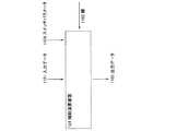
図1に本発明におけるサイドチャネル攻撃を阻止する機能を搭載する対象であるICチップのブロック図を示す。 FIG. 1 shows a block diagram of an IC chip which is a target for mounting a function for preventing side channel attacks in the present invention.
図1において、ICチップ101は、演算回路106、アナログ部115を有する。演算回路106は、CPU102(Central Processing Unit;中央処理装置ともいう。またMPU(microprocessor)ともいう。)、ROM103(Read Only Memory;読み出し専用メモリともいう)、RAM104(Random Access Memory;ランダムアクセスメモリともいう)、補助演算装置124、乱数生成器125、コントローラ105を有する。また、アナログ部115は、アンテナ107、共振回路108、電源回路109、リセット回路110、クロック生成回路111、復調回路112、変調回路113、電源管理回路114を有する。また、コントローラ105は、CPUインターフェース116(CPUIF)、制御レジスタ117、コード抽出回路118、符号化回路119より構成される。なお、図1では、説明の簡略化のため通信信号として、受信信号120と送信信号121とに分けて示したが、実際には両者は重ね合わされており、ICチップ101及びリーダライタ装置の間で同時に送受信される。受信信号120は、アンテナ107と共振回路108とで受信された後、復調回路112により復調される。また、送信信号121は、変調回路113により変調された後、アンテナ107より送信される。なお、受信信号及び送信信号とは、ICチップ側を主体とした表現であり、ICチップが外部からの信号を受信、外部に信号を送信するものであることを付記する。本明細書においては、リーダライタよりICチップが受信する信号、換言すればリーダライタが送信する信号のことを外部からの信号といい、外部からの信号をICチップが受信及びリーダライタが送信することを外部からの信号の送受信という。 In FIG. 1, the
なお、ROMは、リーダライタから受信した受信データを処理する際に機能するプログラム(以下、サイドチャネル攻撃阻止プログラムという)のデータが格納され、RAMにはプログラムが機能した際の処理データが格納される。ROMにはマスクROM等があり、RAMにはスタティック型メモリ(SRAM)やダイナミック型メモリ(DRAM)等がある。具体的には、サイドチャネル攻撃阻止プログラムのデータにはICチップの消費電力の変化を測定するサイドチャネル攻撃の複数のサイドチャネル攻撃阻止のためのルーチン(以下、サイドチャネル攻撃阻止ルーチン)が含まれる。 The ROM stores data of a program (hereinafter referred to as a side channel attack prevention program) that functions when processing received data received from the reader / writer, and the RAM stores processing data when the program functions. The ROM includes mask ROM and the like, and RAM includes static memory (SRAM) and dynamic memory (DRAM). Specifically, the data of the side channel attack prevention program includes a routine for preventing a plurality of side channel attacks of the side channel attack for measuring a change in power consumption of the IC chip (hereinafter referred to as a side channel attack prevention routine). .
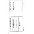
また図2には、ROM103、RAM104のアドレス空間を示す。ROM103には、サイドチャネル攻撃阻止プログラム201、秘密鍵202が格納されている。サイドチャネル攻撃阻止プログラム201は、コマンド判断ルーチン201A、ラウンド判断ルーチン201Bを有する。コマンド判断ルーチン201Aとは、特定のコマンドの判断の処理を実行する機能をもったプログラムコードのことをいう。ラウンド判断ルーチン201Bとは、暗号解読処理におけるラウンド数を判断するための処理を実行する機能をもったプログラムコードのことをいう。これらの複数のルーチンについては、後述することでさらに詳細に説明することにする。 FIG. 2 shows the address space of the
RAM104は、送信データレジスタ203、受信データレジスタ204を有する。送信データレジスタ203は、ICチップが送信するデータを格納する機能を有する。受信データレジスタ204は、ICチップが受信したデータを格納する機能を有する。RAM104は、ROM103に比べて情報量が少ないため、その面積は小さい。 The
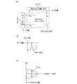
また図3には、リーダライタからICチップに送信される信号、換言するとICチップが受信する信号の構成について示す。受信信号は、SOF301(Start Of Frame;フレームの開始)、フラグ302、コマンド303、データ304、CRC(cyclic redundancy check、巡回冗長検査ともいう)305、EOF306(End Of Frame;フレームの終了)を有する信号である。SOF301,EOF306は単に信号の開始と終了を示すものである。フラグ302はASK、FSK等の変調の種類の情報を有する。コマンド303は、リーダライタがICチップを読み取るか否かを規定する信号であり、信号が読み取られる場合には「インベントリー(Inventory)=1」、それ以外の状態(読み取りを休止する等の命令)では、「インベントリー(Inventory)≠1」との情報を有する。データ304には、暗号解読するデータが含まれる。CRC305はデータの誤認を防止するためにデータより生成される固有のコードの情報を有する。 FIG. 3 shows a configuration of a signal transmitted from the reader / writer to the IC chip, in other words, a signal received by the IC chip. The received signal has SOF301 (Start Of Frame; start of frame),
乱数生成器125は、乱数を生成する機能を有する。具体的には、製造する半導体装置の特性ばらつきを利用することでそのような機能を実現する。なお、半導体装置の特性ばらつきとしては、製造プロセスに起因する種々のばらつき(膜の厚さ、膜の性質、不純物濃度など)を利用する。乱数生成器によるデータは、電気的な読み出し以外の方法で解読することが困難であることから、高いセキュリティを確保する。 The
また図10には、補助演算装置124の構成を示す。補助演算装置124は複数のスイッチマトリクスによって構成され、入力データ1101を鍵1102を使って演算し、出力データ1103として出力する機能を有する。補助演算装置124が演算する時間は、スイッチパラメータ1104の値を元に決まる。具体的には、スイッチパラメータ1104の値を元に複数のスイッチマトリクスを切り替えることでそのような機能を実現する。 FIG. 10 shows the configuration of the auxiliary
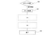
次に、図1におけるICチップでのサイドチャネル攻撃を阻止する機能をもつプログラムの動作を、図4のフローチャートと対応させながら説明する。 Next, the operation of a program having a function of preventing a side channel attack on the IC chip in FIG. 1 will be described in correspondence with the flowchart of FIG.
まず、ICチップが有するリセット回路110は、受信信号120を受けて演算回路106にリセットをかける(初期リセット401)。復調回路112はリセットがかかると受信信号120の復調を開始し、コード抽出回路118へ復調された受信データ122を出力する。コード抽出回路118は復調された受信データ122から制御コードを抽出し制御レジスタ117へ書き込む。 First, the reset circuit 110 included in the IC chip receives the reception signal 120 and resets the arithmetic circuit 106 (initial reset 401). When reset, the demodulation circuit 112 starts demodulating the reception signal 120 and outputs the
ICチップが有するCPU102は、制御レジスタ117にコード抽出回路からの信号の書き込みがあると動作を開始する(開始402)。CPU102は、制御レジスタ117内の制御コードにSOF(Start Of Frame)が含まれていれば(制御レジスタ判断403)、ROM103からサイドチャネル攻撃阻止プログラムを読み込み(プログラム読み込み404)、サイドチャネル攻撃阻止プログラム内のサイドチャネル攻撃阻止ルーチンを実行する(ルーチン実行409)。一方、制御レジスタ117の制御コードにSOFが含まれていなければ初期リセット401後の状態に戻る。なお、CPU102は、サイドチャネル攻撃阻止ルーチンの実行終了後、初期リセット401後の状態に戻る。 The
次に、図1におけるICチップでのサイドチャネル攻撃を阻止する機能を実現するためのサイドチャネル攻撃阻止プログラム内のサイドチャネル攻撃阻止ルーチンを図5〜図9を用いて説明する。 Next, a side channel attack prevention routine in the side channel attack prevention program for realizing the function of preventing the side channel attack in the IC chip in FIG. 1 will be described with reference to FIGS.
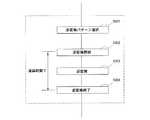
まず、図5に示すフローチャートと対応させながらサイドチャネル攻撃阻止ルーチンの動作を説明する。CPU102は、ROM103からサイドチャネル攻撃阻止プログラムを読み込み、サイドチャネル攻撃阻止ルーチンを開始する(ルーチン開始501)。CPU102は、制御レジスタ117のコマンドコードを読み込み、RAM104へ書き込む(コマンド取得503)。CPU102は、コマンドコードの種類によって処理を暗号解読と暗号解読以外に分岐させ(コマンド判断509)、さらに複数のルーチンを実行させることができる。最後に、CPU102はサイドチャネル攻撃を阻止するための複数のルーチンを終了する(終了504)。 First, the operation of the side channel attack prevention routine will be described with reference to the flowchart shown in FIG. The
次に図6のフローチャートと対応させながら図1におけるICチップでのコマンドコード別処理の詳細を説明する。 Next, the details of the process for each command code in the IC chip in FIG. 1 will be described with reference to the flowchart of FIG.
図6に暗号解読コマンドのフローチャートを示す(図5における(A))。CPU102は、制御レジスタ117のデータコードを読み込み、受信データレジスタ204へ書き込む(データ取得601)。CPU102は、第一の逆変換処理(図6における(D))を実行する。 FIG. 6 shows a flowchart of the decryption command ((A) in FIG. 5). The
次に図7にラウンド判断のフローチャートを示す(図6における(B))。CPU102は、ラウンド(ROUND)フラグ値をN(本実施形態では8)にする。CPU102は、ラウンドフラグ値によって処理を分岐させる(ラウンド判断612)。CPU102は、ラウンドフラグ値が0以外の時には、ラウンド処理(図7における(C))を実行する。CPU102は、ラウンドフラグ値が0の時には、サイドチャネル攻撃阻止ルーチンを終了させる(終了504)。 Next, FIG. 7 shows a flowchart of round judgment ((B) in FIG. 6). The
図8にラウンド処理のフローチャートを示す(図7における(C))。CPU102は、受信データレジスタ204の値を読み出し、第二の逆変換(本実施の形態ではPseudo−Hadamard変換の逆変換)を施し、再び受信データレジスタ204に格納する(第二の逆変換613)。CPU102は、受信データレジスタ204の値を読み出し、逆転置を施し、再び受信データレジスタ204に格納する(逆転置614)。CPU102は、第二の逆変換615を第二の逆変換613、と同じ方法で行う。CPU102は、逆転置616を逆転置614と同じ方法で行う。CPU102は、第二の逆変換617を第二の逆変換613、と同じ方法で行う。CPU102は、第一の逆変換処理(図8における(D))を実行する。CPU102は、ラウンドフラグ値を1減らす。 FIG. 8 shows a flowchart of the round process ((C) in FIG. 7). The
図9に第一の逆変換処理のフローチャートを示す(図6、図8における(D))。CPU102は、補助演算装置124へ受信データレジスタ204の値を逆変換前データとして送信する(逆変換前データ送信621)。補助演算装置124は、CPU102から逆変換前データを受信すると動作を開始する(開始622)。補助演算装置124は、乱数生成器125から乱数値をスイッチパラメータ1104として読み込む(乱数値読み込み623)。補助演算装置124は、スイッチパラメータ1104の値を元に補助演算装置内のスイッチマトリクスを切り替える(スイッチマトリクス切り替え624)。補助演算装置124は、秘密鍵202を鍵1102として読み込む(鍵読み込み625)。補助演算装置124は、逆変換前データを入力データ1101として入力する(データ入力626)。補助演算装置124は、鍵を用いて入力データに逆変換(本実施の形態では45を底とする指数・対数演算と257を基数とする剰余処理の逆変換)を施し(逆変換628)、出力データ1103として出力する(データ出力629)。補助演算装置124は、出力データ1103を逆変換後データとしてCPU102へ送信し動作を終了する(終了630)。CPU102は、補助演算装置124が動作を終了すると逆変換後データを受信し、受信データレジスタ204に格納する(逆変換後データ受信631)。データ入力626からデータ出力629までの時間を補助演算時間Tとする。補助演算装置124では、乱数生成器125から読み込んだ乱数値を元に補助演算時間Tが変化する。 FIG. 9 shows a flowchart of the first inverse transformation process ((D) in FIGS. 6 and 8). The
以上のような形態とすることで、サイドチャネル攻撃を阻止する機能を有するICチップにおいて、乱数生成器と補助演算装置を加えることにより、ICチップから漏れる物理的情報の時間変化をより複雑にする。そのため、第3者が傍受した物理的情報から内部情報を取り出すことに時間がかかり、セキュリティを高めることが出来る。また、サイドチャネル攻撃を阻止する機能を有するICチップにおいて、サイドチャネル攻撃を阻止する方法が変更になることに伴う仕様の変更により、ICチップのマスク設計の段階から作り直す必要がない。そのため、製造コストの削減及び製造時間の短縮ができる。また、マスク設計の変更によって再度作り直したICチップに不具合が生じているといった懸念もない。 By adopting the above configuration, in the IC chip having the function of preventing side channel attacks, the time change of physical information leaking from the IC chip is made more complicated by adding a random number generator and an auxiliary arithmetic unit. . Therefore, it takes time to extract internal information from physical information intercepted by a third party, and security can be improved. Further, in an IC chip having a function for preventing side channel attacks, it is not necessary to recreate the IC chip from the stage of mask design due to a change in specifications accompanying a change in the method for preventing side channel attacks. Therefore, it is possible to reduce the manufacturing cost and the manufacturing time. Further, there is no concern that the IC chip that has been remade due to the change in the mask design has a defect.
また従来においては、サイドチャネル攻撃を阻止する機能を有するICチップを製造する際においては、サイドチャネル攻撃を阻止する回路を搭載することもあった。しかしながら、本発明を採用することで、サイドチャネル攻撃を阻止する機能を読み出し専用メモリにプログラムとして格納することにより、別途サイドチャネル攻撃を阻止する機能を備えた回路を設ける場合より、ICチップを小型化することができる。そのため、ICチップの軽量化、1枚の基板から作製できるICチップの数の増加に伴うコストの削減、またサイドチャネル攻撃を阻止する機能を備えた回路の分だけ、トランジスタ数が減少することによる歩留まりの向上に貢献することができる。 Conventionally, when an IC chip having a function of preventing side channel attacks is manufactured, a circuit for preventing side channel attacks is sometimes mounted. However, by adopting the present invention, the function of preventing side channel attacks is stored as a program in the read-only memory, so that the IC chip can be made smaller than when a circuit having a function of preventing side channel attacks is provided separately. Can be Therefore, the weight of the IC chip is reduced, the cost is reduced with the increase in the number of IC chips that can be manufactured from one substrate, and the number of transistors is reduced by the amount of the circuit having the function of preventing the side channel attack. It can contribute to the improvement of yield.
なお、本実施の形態は、本明細書中の他の実施の形態の記載とも適宜組み合わせて実施することが可能である。 Note that this embodiment can be implemented in combination with any of the other embodiments in this specification as appropriate.
(実施の形態2)
実施の形態1においては、複数のサイドチャネル攻撃阻止ルーチンを有するサイドチャネル攻撃阻止プログラムをROMに格納することによりICチップがサイドチャネル攻撃を阻止する機能を取りうる構成について示した。本実施の形態においては、実施の形態1とは異なる形態のサイドチャネル攻撃を阻止する機能を実現するための装置構成について説明する。フローチャートについては実施の形態1と同様であるため、必要に応じて実施の形態1で述べた図を用いて説明する。(Embodiment 2)
In the first embodiment, the configuration in which the IC chip can take a function of preventing a side channel attack by storing a side channel attack prevention program having a plurality of side channel attack prevention routines in the ROM has been described. In the present embodiment, an apparatus configuration for realizing a function for preventing a side channel attack in a form different from that of the first embodiment will be described. Since the flowchart is the same as that of the first embodiment, the description will be made with reference to the drawings described in the first embodiment as necessary.
図12に本発明におけるサイドチャネル攻撃を阻止する機能を搭載する対象であるICチップのブロック図を示す。図12は実施の形態1における図1のICチップのブロック図から補助演算装置124をのぞいたものであり、図1と同様にCPU102と、ROM103と、RAM104と、乱数生成器125と、からなる演算回路106と、アンテナ107と、共振回路108と、電源回路109と、リセット回路110と、クロック生成回路111と、復調回路112と、変調回路113と、電源管理回路114とからなるアナログ部115と、を有する。コントローラ105は、CPUインターフェース(CPUIF)116と、制御レジスタ117と、コード抽出回路118と、符号化回路119と、から構成される。 FIG. 12 shows a block diagram of an IC chip that is a target for mounting a function for preventing side channel attacks in the present invention. FIG. 12 is a block diagram of the IC chip in FIG. 1 according to the first embodiment except for the auxiliary
このようなICチップにおけるサイドチャネル攻撃を阻止する機能の処理は、実施の形態1と同じであるが、実施の形態1における図9の第一の逆変換処理を補助演算装置124の代わりにCPU102が行う。 The processing of the function for preventing the side channel attack in the IC chip is the same as that of the first embodiment, but the first inverse transformation process of FIG. 9 in the first embodiment is replaced with the
次に、図12におけるICチップでの第一の逆変換処理の動作を、図11のフローチャートと対応させながら説明する。 Next, the operation of the first inverse conversion process in the IC chip in FIG. 12 will be described in correspondence with the flowchart of FIG.
図11においてCPU102は、乱数生成器125の出力値を元に、後述する逆変換1003で使用する逆変換パターンを選択する(逆変換パターン選択1001)。CPU102は、逆変換を開始する(逆変換開始1002)。CPU102は、逆変換パターン選択1001で選択された逆変換パターンと秘密鍵202を用いて受信データレジスタ204の値に逆変換(本実施の形態では45を底とする指数・対数演算と257を基数とする剰余処理の逆変換)を施す(逆変換1003)。CPU102は、逆変換を終了する(逆変換終了1004)。逆変換開始1002から逆変換終了1004までの時間を演算時間Tとする。CPU102では、乱数生成器125から読み込んだ乱数値を元に演算時間Tを変化する。 In FIG. 11, the
これら機能を有するプログラムをROMに含み、CPU102の命令によって処理することで、補助演算装置124の必要が無くなり、補助演算装置124の分だけ回路を小さくすることが可能になる。 A program having these functions is included in the ROM and processed according to instructions from the
以上のような形態とすることで、サイドチャネル攻撃を阻止する機能を有するICチップにおいて、ICチップから漏れる物理的情報の時間変化をより複雑にする。そのため、第3者が傍受した物理的情報から内部情報を取り出すことに時間がかかり、セキュリティを高めることが出来る。また、サイドチャネル攻撃を阻止する機能を有するICチップにおいて、サイドチャネル攻撃を阻止する方法が変更になることに伴う仕様の変更により、ICチップのマスク設計の段階から作り直す必要ない。そのため、製造コストの削減及び製造時間の短縮ができる。また、マスク設計の変更によって再度作り直したICチップに不具合が生じているといった懸念もない。 By adopting the above configuration, in the IC chip having the function of preventing the side channel attack, the time change of physical information leaking from the IC chip is made more complicated. Therefore, it takes time to extract internal information from physical information intercepted by a third party, and security can be improved. Further, in an IC chip having a function for preventing side channel attacks, it is not necessary to recreate the IC chip from the stage of mask design due to a change in specifications accompanying a change in the method for preventing side channel attacks. Therefore, it is possible to reduce the manufacturing cost and the manufacturing time. Further, there is no concern that the IC chip that has been remade due to the change in the mask design has a defect.
また従来においては、サイドチャネル攻撃を阻止する機能を有するICチップを製造する際においては、サイドチャネル攻撃を阻止する回路を搭載することもあった。しかしながら、本発明を採用することで、サイドチャネル攻撃を阻止する機能を読み出し専用メモリにプログラムとして格納することにより、別途サイドチャネル攻撃を阻止する機能を備えた回路を設ける場合より、ICチップを小型化することができる。そのため、ICチップの軽量化、1枚の基板より作製できるICチップの数の増加に伴うコストの削減、またサイドチャネル攻撃を阻止する機能を備えた回路の分だけ、トランジスタ数が減少することによる歩留まりの向上に貢献することができる。 Conventionally, when an IC chip having a function of preventing side channel attacks is manufactured, a circuit for preventing side channel attacks is sometimes mounted. However, by adopting the present invention, the function of preventing side channel attacks is stored as a program in the read-only memory, so that the IC chip can be made smaller than when a circuit having a function of preventing side channel attacks is provided separately. Can be Therefore, the weight of the IC chip is reduced, the cost is reduced with the increase in the number of IC chips that can be manufactured from one substrate, and the number of transistors is reduced by the amount of the circuit having the function of preventing the side channel attack. It can contribute to the improvement of yield.
なお、本実施の形態は、本明細書中の他の実施の形態の記載とも適宜組み合わせて実施することが可能である。 Note that this embodiment can be implemented in combination with any of the other embodiments in this specification as appropriate.
(実施の形態3)
本実施の形態では、絶縁基板上に形成された薄膜トランジスタによりICチップを形成する形態について説明する。(Embodiment 3)
In this embodiment mode, a mode in which an IC chip is formed using a thin film transistor formed over an insulating substrate will be described.
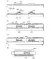
図13(A)に示すように、絶縁基板1300を用意する。絶縁基板1300には、ガラス基板、石英基板、プラスチック基板等が挙げられる。また、これら基板において、その裏面を研磨する等の手法によって薄くすることができる。さらに、金属元素等の導電性基板や、シリコン等の半導体性基板上に絶縁性を有する材料を用いて層を形成した基板を用いることも可能である。ICチップを、例えばプラスチック基板に形成することにより、柔軟性が高く、軽量で薄型な装置を作製することができる。 As shown in FIG. 13A, an insulating
絶縁基板1300上に剥離層1301を選択的に形成する。勿論、剥離層1301を絶縁基板1300全面に形成しても良い。剥離層1301はスパッタリング法やプラズマCVD法等により、タングステン(W)、モリブデン(Mo)、チタン(Ti)、タンタル(Ta)、ニオブ(Nb)、ニッケル(Ni)、コバルト(Co)、ジルコニウム(Zr)、亜鉛(Zn)、ルテニウム(Ru)、ロジウム(Rh)、パラジウム(Pd)、オスミウム(Os)、イリジウム(Ir)、珪素(Si)から選択された元素、又は元素を主成分とする合金材料、又は元素を主成分とする化合物材料からなる層を、単層又は積層して形成する。珪素を含む層の結晶構造は、非晶質、微結晶、多結晶のいずれの場合でもよい。 A
剥離層1301上に下地層1302を形成する。下地層1302は、酸化珪素、窒化珪素、または酸化窒化珪素等の絶縁性を有する材料を用い、単層構造または積層構造で形成することができる。積層構造を用いる場合、下地層1302の一層目として、膜厚10nm以上200nm以下(好ましくは50nm以上100nm以下)の酸化窒化珪素層を形成する。当該酸化窒化珪素層は、プラズマCVD法を用い、SiH4、NH3、N2O及びH2を反応ガスとして形成することができる。次いで下地層1302の二層目として、膜厚50nm以上200nm以下(好ましくは100nm以上150nm以下)の酸化窒化珪素層を形成する。当該酸化窒化珪素層は、プラズマCVD法を用い、SiH4及びN2Oを反応ガスとして形成することができる。A
下地層1302上に半導体層1304を形成する。半導体層1304は、シリコン材料、又はシリコンとゲルマニウムからなる材料等、シリコン半導体層を用いて形成することができる。半導体層1304の結晶構造は非晶質、微結晶、多結晶のいずれでもよい。 A
多結晶の半導体層を形成するには、非晶質半導体層に対して加熱処理を行う手法がある。加熱処理には、レーザ照射、加熱炉、ランプ照射等が挙げられ、これらのいずれか一又は複数を用いることができる。 In order to form a polycrystalline semiconductor layer, there is a method of performing heat treatment on the amorphous semiconductor layer. Examples of the heat treatment include laser irradiation, a heating furnace, lamp irradiation, and the like, and any one or more of them can be used.
レーザ照射には、連続発振型のレーザビーム(CWレーザ)やパルス発振型のレーザビーム(パルスレーザ)を用いることができる。レーザビームとしては、Arレーザ、Krレーザ、エキシマレーザ、YAGレーザ、Y2O3レーザ、YVO4レーザ、YLFレーザ、YA1O3レーザ、ガラスレーザ、ルビーレーザ、アレキサンドライトレーザ、Ti:サファイヤレーザ、銅蒸気レーザまたは金蒸気レーザのうち一種または複数種から発振されるものを用いることができる。このようなレーザビームの基本波と、当該基本波の第2高調波から第4高調波といった高調波のレーザビームのいずれかを照射することで、粒径の大きな結晶を有するシリコン層を得ることができる。高調波には、Nd:YVO4レーザ(基本波1064nm)の第2高調波(532nm)や第3高調波(355nm)を用いることができる。レーザ照射におけるエネルギー密度は0.01〜100MW/cm2程度(好ましくは0.1〜10MW/cm2)が必要である。そして、走査速度を10〜2000cm/sec程度として照射する。For laser irradiation, a continuous wave laser beam (CW laser) or a pulsed laser beam (pulse laser) can be used. As the laser beam, Ar laser, Kr laser, excimer laser, YAG laser, Y2 O3 laser, YVO4 laser, YLF laser, YA1 O3 laser, glass laser, ruby laser, alexandrite laser, Ti: sapphire laser, A laser oscillated from one or more of a copper vapor laser and a gold vapor laser can be used. By irradiating either a fundamental wave of such a laser beam or a harmonic laser beam such as the second harmonic to the fourth harmonic of the fundamental wave, a silicon layer having a crystal with a large grain size is obtained. Can do. As the harmonic, the second harmonic (532 nm) or the third harmonic (355 nm) of an Nd: YVO4 laser (fundamental wave 1064 nm) can be used. Energy density of laser irradiation of about 0.01 to 100 MW / cm2 (preferably 0.1 to 10 MW / cm2) is required. Then, irradiation is performed at a scanning speed of about 10 to 2000 cm / sec.
なお、基本波のCWレーザと高調波のCWレーザとを照射するようにしてもよいし、基本波のCWレーザと高調波のパルスレーザとを照射するようにしてもよい。複数のレーザ光を照射することにより、広範囲のエネルギー領域を補うことができる。 The fundamental CW laser and the harmonic CW laser may be irradiated, or the fundamental CW laser and the harmonic pulse laser may be irradiated. By irradiating a plurality of laser beams, a wide energy range can be compensated.
また、パルスレーザであって、非晶質状態を有するシリコン層がレーザによって溶融してから固化するまでに、次のパルスのレーザを照射できるような発振周波数でレーザを発振させるレーザビームを用いることもできる。このような周波数でレーザを発振させることで、走査方向に向かって連続的に成長した結晶粒を有するシリコン層を得ることができる。このようなレーザの発振周波数は10MHz以上であり、通常用いられている数十Hz〜数百Hzの周波数帯よりも著しく高い。 In addition, a pulse laser that uses a laser beam that oscillates at an oscillation frequency capable of irradiating a laser of the next pulse before the amorphous silicon layer is melted by the laser and solidified is used. You can also. By oscillating the laser at such a frequency, a silicon layer having crystal grains continuously grown in the scanning direction can be obtained. The oscillation frequency of such a laser is 10 MHz or more, which is significantly higher than a frequency band of several tens to several hundreds Hz that is normally used.
加熱処理として加熱炉を用いる場合には、非晶質状態を有する半導体層を400〜550℃で2〜20時間かけて加熱する。このとき、徐々に高温となるように温度を400〜550℃の範囲で多段階に設定するとよい。最初の400℃程度の低温加熱工程により、非晶質状態を有する半導体層に含まれる水素等が出てくるため、結晶化の際に層表面が荒れるのを低減することができる。 In the case of using a heating furnace as the heat treatment, the semiconductor layer having an amorphous state is heated at 400 to 550 ° C. for 2 to 20 hours. At this time, the temperature may be set in multiple stages in the range of 400 to 550 ° C. so that the temperature gradually increases. In the first low-temperature heating process at about 400 ° C., hydrogen and the like contained in the semiconductor layer having an amorphous state are produced, so that the layer surface can be prevented from being roughened during crystallization.
上記加熱処理の工程において、半導体層の結晶化を促進させる金属、例えばニッケル(Ni)を添加する。例えば、非晶質状態を有する珪素層上にニッケルを含む溶液を塗布し、加熱処理を行うことができる。このように金属を用いて加熱処理を行うことで、加熱温度を低減することができ、さらに、結晶粒界の連続した多結晶珪素層を得ることができる。ここで結晶化を促進するための金属としてはNiの他に、鉄(Fe)、ルテニウム(Ru)、ロジウム(Rh)、パラジウム(Pd)、オスミウム(Os)、イリジウム(Ir)、白金(Pt)、銅(Cu)、銀(Au)等を用いることもできる。 In the heat treatment step, a metal that promotes crystallization of the semiconductor layer, for example, nickel (Ni) is added. For example, a solution containing nickel can be applied to a silicon layer having an amorphous state, and heat treatment can be performed. By performing heat treatment using a metal in this manner, the heating temperature can be reduced, and a polycrystalline silicon layer having continuous crystal grain boundaries can be obtained. Here, as a metal for promoting crystallization, in addition to Ni, iron (Fe), ruthenium (Ru), rhodium (Rh), palladium (Pd), osmium (Os), iridium (Ir), platinum (Pt ), Copper (Cu), silver (Au), or the like can also be used.
結晶化を促進させる金属はメモリセル等の汚染源となるため、半導体層を結晶化した後に、金属を除去するゲッタリング工程を行うことが望ましい。ゲッタリング工程では、半導体層を結晶化した後、半導体層上にゲッタリングシンクとなる層を形成し、加熱することで金属をゲッタリングシンクへ移動させる。ゲッタリングシンクには、多結晶半導体層や不純物が添加された半導体層を用いることができる。例えば、多結晶珪素層上にアルゴン等の不活性元素が添加された多結晶半導体層を形成し、これをゲッタリングシンクとして用いることができる。ゲッタリングシンクに不活性元素を添加することによって、ひずみを生じさせ、より効率的に金属を捕獲することができる。また新たにゲッタリングシンクを形成することなく、TFTの半導体層の一部にリン等の元素を添加することによって、金属を捕獲することもできる。 Since the metal that promotes crystallization serves as a contamination source for memory cells and the like, it is desirable to perform a gettering step for removing the metal after the semiconductor layer is crystallized. In the gettering step, after the semiconductor layer is crystallized, a layer to be a gettering sink is formed on the semiconductor layer, and the metal is moved to the gettering sink by heating. As the gettering sink, a polycrystalline semiconductor layer or a semiconductor layer to which an impurity is added can be used. For example, a polycrystalline semiconductor layer to which an inert element such as argon is added can be formed on the polycrystalline silicon layer, and this can be used as a gettering sink. By adding an inert element to the gettering sink, distortion can be generated and the metal can be captured more efficiently. In addition, a metal can be captured by adding an element such as phosphorus to a part of the semiconductor layer of the TFT without forming a new gettering sink.
このように形成された半導体層を、所定の形状に加工し、島状の半導体層1304を形成する。加工手段には、フォトリソグラフィ法によって形成されたマスクを用いて、エッチングする。エッチングには、ウェットエッチング法又はドライエッチング法を適用することができる。 The semiconductor layer thus formed is processed into a predetermined shape, so that an island-shaped
半導体層1304を覆うようにゲート絶縁層1305として機能する絶縁層を形成する。ゲート絶縁層1305は、下地層1302と同様の材料、方法により形成することができる。 An insulating layer functioning as the
図13(B)に示すように、ゲート絶縁層1305を介してゲート電極層1306として機能する導電層を形成する。ゲート電極層1306はアルミニウム(Al)、チタン(Ti)、モリブデン(Mo)、タンタル(Ta)、タングステン(W)もしくはシリコン(Si)の元素からなる膜又はこれらの元素を有する合金膜を用いることができる。ゲート電極層1306は、単層構造又は積層構造とすることができ、積層構造として窒化タンタルとタングステンの積層構造を適用することができる。ゲート電極層1306の加工手段には、フォトリソグラフィ法によって形成されたマスクを用いて、エッチングする。エッチングには、ウェットエッチング法又はドライエッチング法を適用することができる。 As shown in FIG. 13B, a conductive layer functioning as the
ゲート電極層1306の側面にサイドウォール1307と呼ばれる絶縁物を形成する。サイドウォール1307は、下地層1302と同様の材料、方法により形成することができる。またサイドウォール1307の端部にテーパ形状を有するためには、等方性エッチングを用いればよい。サイドウォール1307により、ゲート長が狭くなるにつれて生じる短チャネル効果を防止することができる。短チャネル効果はNチャネル型TFTに顕著であるため、少なくともNチャネル型TFTのゲート電極側面に設けるとよい。 An insulator called a
このような状態で、ゲート絶縁層1305をエッチングする。その結果、半導体層1304の一部や下地層1302が露出する。エッチングには、ウェットエッチング法又はドライエッチング法を適用することができる。 In such a state, the
そして、ゲート電極層1306、及びサイドウォール1307を用いて、半導体層1304に不純物元素を添加し、高濃度不純物領域1310、1312を形成する。Nチャネル型TFTとする場合、不純物元素はリン(P)を用い、Pチャネル型TFTとする場合、不純物元素はボロン(B)を用いることができる。このとき、不純物元素の添加量によっては、サイドウォール1307下方に低濃度不純物領域が形成される。本実施の形態ではNチャネル型の不純物領域にのみ低濃度不純物領域1311を形成する。低濃度不純物領域1311は、短チャネル効果を防止することができるからである。このような低濃度不純物領域を有する構造をLDD(Lightly Doped Drain)構造と呼ぶ。 Then, an impurity element is added to the
その後、下地層1302、半導体層1304、ゲート電極層1306、サイドウォール1307を覆うように絶縁層1314を形成する。絶縁層1314は、CVD法によってシリコンを有する材料から形成するとよい。 After that, an insulating
絶縁層1314を形成後、必要に応じて加熱処理を行う。加熱処理には、上記結晶化と同様な手段を用いることができる。加熱処理により、不純物領域の活性化を行うことができる。CVD法により形成された絶縁層1314は、水素を多く含むため、上記加熱処理により水素が拡散し、不純物領域の膜あれを低減することができる。 After the insulating
図13(C)に示すように、層間膜として機能する絶縁層1315、1316を形成する。絶縁層1315、1316には、無機材料又は有機材料を用いることができる。無機材料は、酸化珪素、窒化珪素、酸化窒化珪素等を用いることができる。有機材料はポリイミド、アクリル、ポリアミド、ポリイミドアミド、レジスト又はベンゾシクロブテン、シロキサン、ポリシラザンを用いることができる。なお、シロキサンとは、シリコン(Si)と酸素(O)との結合で骨格構造が構成される。置換基として、少なくとも水素を含む有機基(例えばアルキル基、芳香族炭化水素)が用いられる。置換基として、フルオロ基を用いてもよい。または置換基として、少なくとも水素を含む有機基と、フルオロ基とを用いてもよい。ポリシラザンは、シリコン(Si)と窒素(N)の結合を有するポリマー材料を出発原料として形成される。無機材料を用いると不純物元素の侵入を防止することができ、有機材料を用いると平坦性を高めることができる。そのため、本実施の形態では、絶縁層1315に無機材料を用い、絶縁層1316に有機材料を用いる。 As shown in FIG. 13C, insulating
絶縁層1314、1315、1316にコンタクトホールを形成して配線1318を形成する。配線1318は、アルミニウム(Al)、チタン(Ti)、モリブデン(Mo)、タンタル(Ta)、タングステン(W)もしくはシリコン(Si)の元素からなる膜又はこれらの元素を有する合金膜を用いることができる。配線1318は、単層構造又は積層構造を用いることができ、例えば第一層にタングステン、窒化タングステン等を用い、第二層にアルミニウムとシリコンの合金(Al−Si)、アルミニウムとチタンの合金(Al−Ti)を用い、第三層に窒化チタン膜、チタン膜等を順次積層した構造を適用することができる。配線1318の加工には、フォトリソグラフィ法で形成されたマスクを用いて、エッチングする。エッチングには、ウェットエッチング法又はドライエッチング法を適用することができる。配線1318は、半導体層1304では不純物領域に接続し、このような配線をソース電極、ドレイン電極と呼ぶことができる。 Contact holes are formed in the insulating
このようにして、Nチャネル型TFT1330、Pチャネル型TFT1331を形成することができる。 In this manner, an N-
その後必要に応じて、配線1318上に保護膜1319を形成する。保護膜1319は、珪素を有する酸化物、又は珪素を有する窒化物によって形成することができる。例えば、窒化珪素を用いて保護膜1319を形成する。その結果、水分や酸素の侵入を防止することができる。 Thereafter, a
図13(D)に示すように、TFT間に開口部を形成し、エッチング剤1325を導入する。開口部はウェットエッチング法又はドライエッチング法を用いて形成することができる。なお開口部の形成位置は、TFT間でなくともよく、半導体層1304が形成されない領域であればよい。エッチング剤1325は、ウェットエッチング法であれば、フッ酸を水やフッ化アンモニウムで希釈した混液、フッ酸と硝酸の混液、フッ酸と硝酸と酢酸の混液、過酸化水素と硫酸の混液、過酸化水素とアンモニウム水と水の混液、過酸化水素と塩酸と水の混液等を用いる。また、ドライエッチング法であれば、フッ素等のハロゲン系の原子や分子を含む気体、又は酸素を含む気体を用いる。好ましくは、エッチング剤として、フッ化ハロゲン又はハロゲン間化合物を含む気体又は液体、例えば三フッ化塩素(ClF3)を適用することができる。As shown in FIG. 13D, an opening is formed between the TFTs, and an
エッチング剤を導入することにより、剥離層1301が除去される。すると、絶縁基板1300が剥離される。このようにして、薄型化、軽量化を達成したICチップを形成することができる。 By introducing the etching agent, the
エッチング剤を導入する方法以外に、レーザ描画により剥離層1301を露出させたり、ICチップの側面に切り込みを入れる等して、物理的に絶縁基板1300を剥離させてもよい。 In addition to the method of introducing an etchant, the insulating
図13(E)に示すように、フィルム1327、1328によって覆い、ICチップを完成させることができる。このとき、接着層1329を用いて、フィルム1327や1328と貼り合わせてもよい。フィルム1327、1328には、水分や酸素等の侵入を防ぐために、保護膜を形成しても良い。また配線1318上には保護膜1319が形成されているため、下地層1302又は接着層1329の下方に保護膜を形成してもよい。保護膜は、珪素を有する酸化物、又は珪素を有する窒化物によって形成することができる。 As shown in FIG. 13E, an IC chip can be completed by covering with
このように絶縁基板上、さらに絶縁基板を剥離したICチップは、より軽量で安価に提供することができる。またこのようなICチップは柔軟性に富むため、曲面に貼り付けることも可能である。 Thus, the IC chip from which the insulating substrate is further peeled off can be provided at a lower weight and at a lower cost. Further, since such an IC chip is flexible, it can be attached to a curved surface.
また、本実施の形態は、本明細書中の他の実施の形態の記載とも適宜組み合わせて実施することが可能である。そのため、本発明の半導体装置のサイドチャネル攻撃を阻止する機能を有するICチップにおいて、ICチップから漏れる物理的情報の時間変化をより複雑にする。そのため、第3者が傍受した物理的情報から内部情報を取り出すことに時間がかかり、セキュリティを高めることが出来る。また、サイドチャネル攻撃を阻止する機能を有するICチップにおいて、サイドチャネル攻撃を阻止する方法が変更になることに伴う仕様の変更により、ICチップのマスク設計の段階から作り直す必要がなくなる。そのため、製造コストの削減及び製造時間の短縮ができる。また、マスク設計の変更によって再度作り直したICチップに不具合が生じているといった懸念もない。 In addition, this embodiment can be implemented in combination with any of the other embodiments in this specification as appropriate. Therefore, in the IC chip having the function of preventing the side channel attack of the semiconductor device of the present invention, the time change of physical information leaking from the IC chip is made more complicated. Therefore, it takes time to extract internal information from physical information intercepted by a third party, and security can be improved. In addition, in an IC chip having a function for preventing side channel attacks, it is not necessary to recreate the IC chip from the stage of mask design due to a change in specifications accompanying a change in the method for preventing side channel attacks. Therefore, it is possible to reduce the manufacturing cost and the manufacturing time. Further, there is no concern that the IC chip that has been remade due to the change in the mask design has a defect.
また従来においては、サイドチャネル攻撃を阻止する機能を有するICチップを製造する際においては、サイドチャネル攻撃を阻止する回路を搭載することもあった。しかしながら、本発明を採用することで、サイドチャネル攻撃を阻止する機能を読み出し専用メモリにプログラムとして格納することにより、別途サイドチャネル攻撃を阻止する機能を備えた回路を設ける場合より、ICチップを小型化することができる。そのため、ICチップの軽量化、1枚の基板より作製できるICチップの数の増加に伴うコストの削減、またサイドチャネル攻撃を阻止する機能を備えた回路の分だけ、トランジスタ数が減少することによる歩留まりの向上などに貢献することができる。 Conventionally, when an IC chip having a function of preventing side channel attacks is manufactured, a circuit for preventing side channel attacks is sometimes mounted. However, by adopting the present invention, the function of preventing side channel attacks is stored as a program in the read-only memory, so that the IC chip can be made smaller than when a circuit having a function of preventing side channel attacks is provided separately. Can be Therefore, the weight of the IC chip is reduced, the cost is reduced with the increase in the number of IC chips that can be manufactured from one substrate, and the number of transistors is reduced by the amount of the circuit having the function of preventing the side channel attack. It can contribute to the improvement of yield.
(実施の形態4)
本実施の形態では、単結晶シリコンに形成されたトランジスタによりICチップを形成する形態について図14を用いて説明する。(Embodiment 4)
In this embodiment mode, a mode in which an IC chip is formed using a transistor formed in single crystal silicon is described with reference to FIGS.
まず、図14(A)を用いて、トランジスタの作製工程について説明する。単結晶のシリコン基板1901を用意する。そして、シリコン基板1901の主面(素子形成面または回路形成面)の第1の素子形成領域にn型ウェル1902を、第2の素子形成領域にp型ウェル1903をそれぞれ選択的に形成する。また、シリコン基板1901の裏面を研磨する等の手法によって薄くすることも可能である。予め、シリコン基板1901を薄膜化することによって、軽量で薄型な半導体装置を作製することができる。 First, a manufacturing process of a transistor is described with reference to FIG. A single
次いで、第1の素子形成領域と第2の素子形成領域とを区画するための素子分離領域となるフィールド酸化膜1904を形成する。フィールド酸化膜1904は厚い熱酸化膜であり、LOCOS(local oxidation of silicon)法を用いて形成すればよい。なお、素子分離法は、LOCOS法に限定されず、例えば素子分離領域はトレンチ分離法を用いてトレンチ構造を有していてもよいし、LOCOS構造とトレンチ構造の組み合わせであってもよい。 Next, a
次いで、シリコン基板の表面を、例えば熱酸化させることによってゲート絶縁膜を形成する。ゲート絶縁膜は、CVD法を用いて形成してもよく、酸化窒化珪素膜や酸化珪素膜や窒化珪素膜やそれらの積層膜を用いることができる。 Next, a gate insulating film is formed by thermally oxidizing the surface of the silicon substrate, for example. The gate insulating film may be formed by a CVD method, and a silicon oxynitride film, a silicon oxide film, a silicon nitride film, or a stacked film thereof can be used.
次いで、ポリシリコン層1905b、1906bとシリサイド層1905a、1906aとの積層膜を全面に形成し、リソグラフィ技術およびドライエッチング技術に基づき積層膜を形成することによってゲート絶縁膜上にポリサイド構造を有するゲート電極1905、1906を形成する。ポリシリコン層1905b、1906bは低抵抗化するために予め、1021/cm3程度の濃度でリン(P)をドープしておいても良いし、ポリシリコン膜を形成した後で濃いn型不純物を拡散させても良い。また、シリサイド層1905a、1906aを形成する材料はモリブデンシリサイド(MoSix)、タングステンシリサイド(WSix)、タンタルシリサイド(TaSix)、チタンシリサイド(TiSix)などを適用することが可能である。Next, a stacked film of
次いで、エクステンション領域を形成するために、ゲート絶縁膜を介してシリコン半導体基板にイオン注入を行う。本実施例においては、各ソース領域およびドレイン領域とチャネル形成領域との間に形成された不純物領域をエクステンション領域と呼ぶ。エクステンション領域1907、1908の不純物濃度は、ソース領域およびドレイン領域の不純物濃度よりも低い場合もあるし、同等の場合もあるし、高い場合もある。即ち、エクステンション領域の不純物濃度は、半導体装置に要求される特性に基づいて決定すればよい。 Next, in order to form an extension region, ion implantation is performed on the silicon semiconductor substrate through the gate insulating film. In this embodiment, the impurity region formed between each source region and drain region and the channel formation region is called an extension region. The impurity concentration of the
本実施例は、本発明に適用されるCMOS回路を製造する場合であるので、pチャネル型FETを形成すべき第1の素子形成領域をレジスト材料で被覆し、n型不純物であるヒ素(As)やリン(P)をシリコン基板に注入する。また、nチャネル型FETを形成すべき第2の素子形成領域をレジスト材料で被覆し、p型不純物であるボロン(B)をシリコン基板に注入する。 Since this embodiment is a case of manufacturing a CMOS circuit applied to the present invention, the first element formation region in which the p-channel FET is to be formed is covered with a resist material, and arsenic (As ) Or phosphorus (P) is implanted into the silicon substrate. Further, the second element formation region in which the n-channel FET is to be formed is covered with a resist material, and boron (B) that is a p-type impurity is implanted into the silicon substrate.
次いで、イオン注入された不純物の活性化および、イオン注入によって発生したシリコン基板における結晶欠陥を回復するために、第1回目の活性化処理を行う。Siの融点程度の温度まで半導体基板を加熱して活性化する。 Next, a first activation process is performed in order to activate the ion-implanted impurities and recover crystal defects in the silicon substrate generated by the ion implantation. The semiconductor substrate is heated to a temperature about the melting point of Si and activated.
次いで、ゲート電極の側壁にサイドウォール1909、1910を形成する。例えば酸化珪素からなる絶縁材料層を全面にCVD法にて堆積させ、かかる絶縁材料層をエッチバックすることによってサイドウォールを形成すればよい。エッチバックの際に自己整合的にゲート絶縁膜を選択的に除去してもよい。また、エッチバック後にゲート絶縁膜のエッチングを行ってもよい。こうして、ゲート電極の幅と、そのゲート電極の側壁の両側に設けられたサイドウォールの幅とを合計した幅を有するゲート絶縁膜1911、1912が形成される。 Next, sidewalls 1909 and 1910 are formed on the sidewalls of the gate electrode. For example, an insulating material layer made of silicon oxide may be deposited on the entire surface by a CVD method, and the insulating material layer may be etched back to form the sidewall. The gate insulating film may be selectively removed in a self-aligned manner during the etch back. Further, the gate insulating film may be etched after the etch back. Thus,
次いで、ソース領域およびドレイン領域を形成するために、露出したシリコン基板にイオン注入を行う。pチャネル型FETを形成すべき第1の素子形成領域をレジスト材料で被覆し、n型不純物であるヒ素(As)やリン(P)をシリコン基板に注入してソース領域1913及びドレイン領域1914を形成する。また、nチャネル型FETを形成すべき第2の素子形成領域をレジスト材料で被覆し、p型不純物であるボロン(B)をシリコン基板に注入してソース領域1915及びドレイン領域1916を形成する。 Next, ion implantation is performed on the exposed silicon substrate to form a source region and a drain region. A first element formation region in which a p-channel FET is to be formed is covered with a resist material, and n-type impurities such as arsenic (As) and phosphorus (P) are implanted into the silicon substrate to form a
次いで、イオン注入された不純物の活性化および、イオン注入によって発生したシリコン基板における結晶欠陥を回復するために、第2回目の活性化処理を行う。 Next, a second activation process is performed in order to activate the ion-implanted impurities and recover crystal defects in the silicon substrate generated by the ion implantation.
そして、活性化後に層間絶縁膜やプラグ電極やメタル配線等を形成する。第1の層間絶縁膜1917は、プラズマCVD法や減圧CVD法を用いて酸化シリコン膜や酸化窒化シリコン膜などを形成する。さらにその上にリンガラス(PSG)、あるいはボロンガラス(BSG)、もしくはリンボロンガラス(PBSG)の第2の層間絶縁膜1918が形成する。第2の層間絶縁膜1918は、平坦性を上げるため、スピンコート法や常圧CVD法で作製する。なお、層間絶縁膜は単層であってもよいし、3層以上の多層構造であってもよい。 Then, after activation, an interlayer insulating film, a plug electrode, a metal wiring, and the like are formed. As the first
ソース電極1919、1921、及びドレイン電極1920、1922は、第1の層間絶縁膜1917および第2の層間絶縁膜1918にそれぞれのFETのソース領域及びドレイン領域に達するコンタクトホールを形成した後に形成するもので、低抵抗材料として通常良く用いられるアルミニウム(Al)を用いると良い。また、Alとチタン(Ti)の積層構造としても良い。 The
なお、コンタクト穴は、電子線直接描画技術によって形成してもよい。電子線直接描画は、ポジ型の電子線描画用レジストを第1の層間絶縁膜1917及び第2の層間絶縁膜1918上の全面に形成し、電子線が照射された部分を現像液によって溶解させる。そして、コンタクト穴が形成される箇所のレジストに穴が空き、レジストをマスクとしてドライエッチングを行なうことにより、所定の位置の第1の層間絶縁膜1917及び第2の層間絶縁膜1918がエッチングされてコンタクト穴を形成することができる。 The contact hole may be formed by an electron beam direct drawing technique. In the direct electron beam drawing, a positive electron beam drawing resist is formed on the entire surface of the first
最後に、パッシベーション膜1923を形成する。図14(A)において向かって左側がpチャネル型トランジスタ1925であり、右側がnチャネル型トランジスタ1926である。 Finally, a
パッシベーション膜1923は、プラズマCVD法で窒化シリコン膜、または酸化シリコン膜、あるいは窒化酸化シリコン膜で形成されている。また、窒化シリコン膜等の代わりに有機樹脂膜、若しくはパッシベーション膜の上に有機樹脂膜を積層してもよい。有機樹脂材料として、ポリイミド、ポリアミド、アクリル、ベンゾシクロブテン(BCB)などを用いることができる。有機樹脂膜を用いる利点は、膜の形成方法が簡単である点や、比誘電率が低いので寄生容量を低減できる点、平坦化するのに適している点などがある。勿論、上述した以外の有機樹脂膜を用いても良い。 The
このようにして、単結晶基板上にpチャネル型トランジスタ1925とnチャネル型トランジスタ1926を形成することができる。 In this manner, the p-channel transistor 1925 and the n-channel transistor 1926 can be formed over the single crystal substrate.
なお、pチャネル型トランジスタ1925とnチャネル型トランジスタ1926の作製された基板において、その裏面を研磨する等の手法によってさらに半導体装置を薄くしてもよい。シリコン基板をさらに薄膜化することによって、軽量で薄型な半導体装置を作製することができる。 Note that the semiconductor device may be further thinned by a method such as polishing the back surface of the substrate over which the p-channel transistor 1925 and the n-channel transistor 1926 are formed. By thinning the silicon substrate further, a light and thin semiconductor device can be manufactured.
そして、図14(B)に示すように、フィルム1927、1928によって覆い、ICチップを完成させることができる。フィルム1927、1928には、水分や酸素等の侵入を防ぐために、保護膜を形成しても良い。保護膜は、珪素を有する酸化物、又は珪素を有する窒化物によって形成することができる。また、フィルムにはICチップのアンテナとなるパターンが形成されていてもよい。 Then, as shown in FIG. 14B, the film can be covered with
このように単結晶基板上に形成されたICチップは、軽量でより小型化された製品を提供することができる。またこのようなICチップは小型化された半導体装置を作成することができ、トランジスタのばらつきも小さいため、好適である。 Thus, the IC chip formed on the single crystal substrate can provide a lighter and more compact product. Such an IC chip is preferable because a miniaturized semiconductor device can be manufactured and variation in transistors is small.
また、本実施の形態は、本明細書中の他の実施の形態の記載とも適宜組み合わせて実施することが可能である。そのため、本発明の半導体装置のサイドチャネル攻撃を阻止する機能を有するICチップにおいて、ICチップから漏れる物理的情報の時間変化をより複雑にする。そのため、第3者が傍受した物理的情報から内部情報を取り出すことに時間がかかり、セキュリティを高めることが出来る。また、サイドチャネル攻撃を阻止する機能を有するICチップにおいて、サイドチャネル攻撃を阻止する方法が変更になることに伴う仕様の変更により、ICチップのマスク設計の段階から作り直す必要がなくなる。そのため、製造コストの削減及び製造時間の短縮ができる。また、マスク設計の変更によって再度作り直したICチップに不具合が生じているといった懸念もない。 In addition, this embodiment can be implemented in combination with any of the other embodiments in this specification as appropriate. Therefore, in the IC chip having the function of preventing the side channel attack of the semiconductor device of the present invention, the time change of physical information leaking from the IC chip is made more complicated. Therefore, it takes time to extract internal information from physical information intercepted by a third party, and security can be improved. In addition, in an IC chip having a function for preventing side channel attacks, it is not necessary to recreate the IC chip from the stage of mask design due to a change in specifications accompanying a change in the method for preventing side channel attacks. Therefore, it is possible to reduce the manufacturing cost and the manufacturing time. Further, there is no concern that the IC chip that has been remade due to the change in the mask design has a defect.
また従来においては、サイドチャネル攻撃を阻止する機能を有するICチップを製造する際においては、サイドチャネル攻撃を阻止する回路を搭載することもあった。しかしながら、本発明を採用することで、サイドチャネル攻撃を阻止する機能を読み出し専用メモリにプログラムとして格納することにより、サイドチャネル攻撃を阻止する機能を備えた回路の分だけ、ICチップを小型化することができる。そのため、ICチップの軽量化、1枚の基板から作製できるICチップの数の増加に伴うコストの削減、またサイドチャネル攻撃を阻止する機能を備えた回路の分だけ、トランジスタ数が減少することによる歩留まりの向上に貢献することができる。 Conventionally, when an IC chip having a function of preventing side channel attacks is manufactured, a circuit for preventing side channel attacks is sometimes mounted. However, by adopting the present invention, the function for preventing side channel attacks is stored as a program in the read-only memory, thereby reducing the size of the IC chip by the amount of the circuit having the function for preventing side channel attacks. be able to. Therefore, the weight of the IC chip is reduced, the cost is reduced with the increase in the number of IC chips that can be manufactured from one substrate, and the number of transistors is reduced by the amount of the circuit having the function of preventing the side channel attack. It can contribute to the improvement of yield.
(実施の形態5)
本実施の形態では、本発明における半導体装置の例として、暗号処理機能を有するICチップについて図15を用いて説明する。(Embodiment 5)
In this embodiment, an IC chip having a cryptographic processing function will be described with reference to FIG. 15 as an example of a semiconductor device in the present invention.
まず、図15を用いてICチップのブロック構成を説明する。図15において、ICチップ101は、CPU102と、ROM103と、RAM104と、コントローラ105と、からなる演算回路106と、アンテナ107と、共振回路108と、電源回路109と、リセット回路110と、クロック生成回路111と、復調回路112と、変調回路113と、電源管理回路114と、からなるアナログ部115と、を有する。コントローラ105は、CPUインターフェース(CPUIF)116と、制御レジスタ117と、コード抽出回路118と、符号化回路119と、から構成される。なお、図15では、説明の簡単化のため、通信信号を受信信号120と、送信信号121とに分けて示したが、実際には、両者は重ね合わされており、ICチップ101及びリーダライタの間で同時に送受信される。受信信号120は、アンテナ107と共振回路108とで受信された後、復調回路112により復調される。また、送信信号121は、変調回路113により変調された後、アンテナ107より送信される。 First, the block configuration of the IC chip will be described with reference to FIG. In FIG. 15, an
図15において、通信信号により形成される磁界中にICチップ101を置くと、アンテナ107と共振回路108により、誘導起電力を生じる。誘導起電力は、電源回路109における電気容量により保持され、また電気容量によって電位が安定化され、ICチップ101の各回路に電源電圧として供給される。リセット回路110は、ICチップ101全体の初期リセット信号を生成する。例えば、電源電圧の上昇に遅延して立ち上がる信号をリセット信号として生成する。クロック生成回路111は、電源管理回路114より生成される制御信号に応じて、クロック信号の周波数とデューティー比を変更する。復調回路112は、ASK方式の受信信号120の振幅の変動を”0”/”1”の受信データ122として検出する。復調回路112は、例えばローパスフィルターとする。さらに、変調回路113は、送信データをASK方式の送信信号121の振幅を変動させて送信する。例えば、送信データ123が”0”の場合、共振回路108の共振点を変化させ、通信信号の振幅を変化させる。電源管理回路114は、電源回路109より演算回路106に供給される電源電圧または演算回路106における消費電流を監視し、クロック生成回路111において、クロック信号の周波数とデューティー比を変更するための制御信号を生成する。 In FIG. 15, when the
本実施の形態におけるICチップの動作を説明する。まず、ICチップ101は、リーダライタより送信された暗号文データを含む受信信号120を受信する。受信信号120は、復調回路112で復調された後、コード抽出回路118で制御コマンドや暗号文のデータなどに分解され、制御レジスタ117に格納される。ここで、制御コマンドは、ICチップ101の応答を指定するデータである。例えば、固有ID番号の送信、動作停止、暗号解読などを指定する。ここでは、暗号解読に指定した制御コマンドを受信したとする。 The operation of the IC chip in this embodiment will be described. First, the
続いて、演算回路106において、CPU102が、ROM103に格納された暗号解読プログラムにしたがって、ROM103にあらかじめ格納された秘密鍵3001を用いて暗号文を解読(復号)する。復号された暗号文(復号文)は、制御レジスタ117に格納される。この際、RAM104をデータ格納領域として用いる。なお、CPU102は、CPUIF116を介してROM103、RAM104、制御レジスタ117にアクセスする。CPUIF116は、CPU102が要求するアドレスより、ROM103、RAM104、制御レジスタ117のいずれかに対するアクセス信号を生成する機能を有している。 Subsequently, in the arithmetic circuit 106, the
最後に、符号化回路119において、復号文から送信データ123を生成し、変調回路113で変調し、アンテナ107より送信信号121をリーダライタに送信する。 Finally, in the
なお、本実施の形態では、演算方式として、ソフトウェア的に処理する方式、すなわち、CPUと大規模メモリとで演算回路を構成し、プログラムをCPUで実行する方式について説明したが、目的に応じて最適な演算方式を選び、当該方式に基づいて構成することも可能である。例えば、演算方式として、他にも、演算をハードウェア的に処理する方式と、ハードウェア及びソフトウェアを併用する方式と、が考えられる。ハードウェア的に処理する方式では、専用回路で演算回路を構成すれば良い。ハードウェア及びソフトウェアを併用する方式では、専用回路と、CPUと、メモリと、で演算回路を構成し、専用回路で演算処理の一部分を行い、残りの演算処理のプログラムをCPUで実行すれば良い。 In the present embodiment, as a calculation method, a method of processing in software, that is, a method of configuring a calculation circuit with a CPU and a large-scale memory and executing a program with the CPU has been described. It is also possible to select an optimal calculation method and configure based on the method. For example, as a calculation method, other methods such as a method of processing the operation in hardware and a method of using both hardware and software are conceivable. In the method of processing in hardware, an arithmetic circuit may be configured with a dedicated circuit. In the method using both hardware and software, a dedicated circuit, a CPU, and a memory constitute an arithmetic circuit, a part of the arithmetic processing is performed by the dedicated circuit, and the remaining arithmetic processing program is executed by the CPU. .
また、本実施の形態は、本明細書中の他の実施の形態の記載とも適宜組み合わせて実施することが可能である。そのため、本発明の半導体装置のサイドチャネル攻撃を阻止する機能を有するICチップにおいて、ICチップから漏れる物理的情報の時間変化をより複雑にする。そのため、第3者が傍受した物理的情報から内部情報を取り出すことに時間がかかり、セキュリティを高めることが出来る。また、サイドチャネル攻撃を阻止する機能を有するICチップにおいて、サイドチャネル攻撃を阻止する方法が変更になることに伴う仕様の変更により、ICチップのマスク設計の段階から作り直す必要ない。そのため、製造コストの削減及び製造時間の短縮ができる。また、マスク設計の変更によって再度作り直したICチップに不具合が生じているといった懸念もない。 In addition, this embodiment can be implemented in combination with any of the other embodiments in this specification as appropriate. Therefore, in the IC chip having the function of preventing the side channel attack of the semiconductor device of the present invention, the time change of physical information leaking from the IC chip is made more complicated. Therefore, it takes time to extract internal information from physical information intercepted by a third party, and security can be improved. Further, in an IC chip having a function for preventing side channel attacks, it is not necessary to recreate the IC chip from the stage of mask design due to a change in specifications accompanying a change in the method for preventing side channel attacks. Therefore, it is possible to reduce the manufacturing cost and the manufacturing time. Further, there is no concern that the IC chip that has been remade due to the change in the mask design has a defect.
また従来においては、サイドチャネル攻撃を阻止する機能を有するICチップを製造する際においては、サイドチャネル攻撃を阻止する回路を搭載することもあった。しかしながら、本発明を採用することで、サイドチャネル攻撃を阻止する機能を読み出し専用メモリにプログラムとして格納することにより、別途サイドチャネル攻撃を阻止する機能を備えた回路を設ける場合より、ICチップを小型化することができる。そのため、ICチップの軽量化、1枚の基板から作製できるICチップの数の増加に伴うコストの削減、またサイドチャネル攻撃を阻止する機能を備えた回路の分だけ、トランジスタ数が減少することによる歩留まりの向上に貢献することができる。 Conventionally, when an IC chip having a function of preventing side channel attacks is manufactured, a circuit for preventing side channel attacks is sometimes mounted. However, by adopting the present invention, the function of preventing side channel attacks is stored in the read-only memory as a program, so that the IC chip can be made smaller than when a circuit having a function of preventing side channel attacks is provided separately. Can be Therefore, the weight of the IC chip is reduced, the cost is reduced with the increase in the number of IC chips that can be manufactured from one substrate, and the number of transistors is reduced by the amount of the circuit having the function of preventing the side channel attack. It can contribute to the improvement of yield.
(実施の形態6)
アンテナは、電波法に定められた範囲内で目的に見合った大きさ、形状であればよい。送受信される信号は、125kHz、13.56MHz、915MHz、2.45GHzなどがあり、それぞれISO規格などが設定される。具体的なアンテナとしては、ダイポールアンテナ、パッチアンテナ、ループアンテナ、八木アンテナなどを用いればよい。本実施の形態では、ICチップに接続されるアンテナ形状について説明する。(Embodiment 6)
The antenna may be any size and shape that meets the purpose within the range stipulated by the Radio Law. Signals to be transmitted and received include 125 kHz, 13.56 MHz, 915 MHz, 2.45 GHz, and the like, and ISO standards are set for each. As a specific antenna, a dipole antenna, a patch antenna, a loop antenna, a Yagi antenna, or the like may be used. In this embodiment mode, a shape of an antenna connected to an IC chip will be described.
図16(A)にICチップ1601に接続されるアンテナ1602を示す。図16(A)において、ICチップ1601が中心部に設けられ、アンテナ1602はICチップ1601の接続端子に接続されている。アンテナの長さを確保するため、アンテナ1602は矩形状に折れ曲がっている。 FIG. 16A illustrates an
図16(B)には、ICチップ1601が一端側に設けられ、アンテナ1603はICチップ1601の接続端子に接続されている。アンテナの長さを確保するため、アンテナ1603は矩形状に折れ曲がっている。 In FIG. 16B, an
図16(C)には、ICチップ1601の両端に矩形状に折れ曲がったアンテナ1604が設けられている。 In FIG. 16C,
図16(D)には、ICチップ1601の両端に直線上のアンテナ1605が設けられている。 In FIG. 16D,
このようにアンテナの形状はICチップの構造若しくは偏波、又は用途に見合ったものを選択すればよい。そのため、ダイポールアンテナであれば折り返しダイポールアンテナであってもよい。ループアンテナであれば、円形ループアンテナ、方形ループアンテナであってもよい。パッチアンテナであれば円形パッチアンテナ、方形アンテナであってもよい。 As described above, the shape of the antenna may be selected in accordance with the structure or polarization of the IC chip or the application. Therefore, a folded dipole antenna may be used as long as it is a dipole antenna. As long as it is a loop antenna, it may be a circular loop antenna or a square loop antenna. If it is a patch antenna, a circular patch antenna or a square antenna may be used.
パッチアンテナの場合、セラミック等の誘電材料を用いたアンテナを用いればよい。パッチアンテナの基板として用いる誘電材料の誘電率を高くすることによってアンテナを小型化することができる。また、パッチアンテナの場合、機械強度が高いため、繰り返し使用することが可能である。 In the case of a patch antenna, an antenna using a dielectric material such as ceramic may be used. The antenna can be miniaturized by increasing the dielectric constant of the dielectric material used as the patch antenna substrate. In the case of the patch antenna, since the mechanical strength is high, it can be used repeatedly.
パッチアンテナの誘電材料は、セラミック、有機樹脂、又はセラミックと有機樹脂の混合物等で形成することができる。セラミックの代表例としては、アルミナ、ガラス、フォルステライト等が挙げられる。さらには、複数のセラミックを混合して用いてもよい。また、高い誘電率を得るためには、誘電体層を、強誘電体材料で形成することが好ましい。強誘電体材料の代表例としては、チタン酸バリウム(BaTiO3)、チタン酸鉛(PbTiO3)、チタン酸ストロンチウム(SrTiO3)、ジルコン酸鉛(PbZrO3)、ニオブ酸リチウム(LiNbO3)、チタン酸ジルコン鉛(PZT)等が挙げられる。さらには、複数の強誘電体材料を混合して用いてもよい。The dielectric material of the patch antenna can be formed of ceramic, organic resin, a mixture of ceramic and organic resin, or the like. Representative examples of ceramics include alumina, glass, forsterite and the like. Furthermore, a plurality of ceramics may be mixed and used. In order to obtain a high dielectric constant, the dielectric layer is preferably formed of a ferroelectric material. Typical examples of the ferroelectric material include barium titanate (BaTiO3 ), lead titanate (PbTiO3 ), strontium titanate (SrTiO3 ), lead zirconate (PbZrO3 ), lithium niobate (LiNbO3 ), Examples include lead zirconate titanate (PZT). Further, a plurality of ferroelectric materials may be mixed and used.
また、本実施の形態は、本明細書中の他の実施の形態の記載とも適宜組み合わせて実施することが可能である。そのため、本発明の半導体装置のサイドチャネル攻撃を阻止する機能を有するICチップにおいて、ICチップから漏れる物理的情報の時間変化をより複雑にする。そのため、第3者が傍受した物理的情報から内部情報を取り出すことに時間がかかり、セキュリティを高めることが出来る。また、サイドチャネル攻撃を阻止する機能を有するICチップにおいて、サイドチャネル攻撃を阻止する方法が変更になることに伴う仕様の変更により、ICチップのマスク設計の段階から作り直す必要ない。そのため、製造コストの削減及び製造時間の短縮ができる。また、マスク設計の変更によって再度作り直したICチップに不具合が生じているといった懸念もない。 In addition, this embodiment can be implemented in combination with any of the other embodiments in this specification as appropriate. Therefore, in the IC chip having the function of preventing the side channel attack of the semiconductor device of the present invention, the time change of physical information leaking from the IC chip is made more complicated. Therefore, it takes time to extract internal information from physical information intercepted by a third party, and security can be improved. Further, in an IC chip having a function for preventing side channel attacks, it is not necessary to recreate the IC chip from the stage of mask design due to a change in specifications accompanying a change in the method for preventing side channel attacks. Therefore, it is possible to reduce the manufacturing cost and the manufacturing time. Further, there is no concern that the IC chip that has been remade due to the change in the mask design has a defect.
また従来においては、サイドチャネル攻撃を阻止する機能を有するICチップを製造する際においては、サイドチャネル攻撃を阻止する回路を搭載することもあった。しかしながら、本発明を採用することで、サイドチャネル攻撃を阻止する機能を読み出し専用メモリにプログラムとして格納することにより、別途サイドチャネル攻撃を阻止する機能を備えた回路を設ける場合より、ICチップを小型化することができる。そのため、ICチップの軽量化、1枚の基板から作製できるICチップの数の増加に伴うコストの削減、サイドチャネル攻撃を阻止する機能を備えた回路の分だけ、トランジスタ数が減少することによる歩留まりの向上に貢献することができる。 Conventionally, when an IC chip having a function of preventing side channel attacks is manufactured, a circuit for preventing side channel attacks is sometimes mounted. However, by adopting the present invention, the function of preventing side channel attacks is stored as a program in the read-only memory, so that the IC chip can be made smaller than when a circuit having a function of preventing side channel attacks is provided separately. Can be For this reason, the yield due to the reduction in the number of transistors by the weight of the IC chip, the cost reduction associated with the increase in the number of IC chips that can be manufactured from one substrate, and the circuit with the function of preventing side channel attacks. It can contribute to improvement.
(実施の形態7)
アンテナについて、実施の形態6で説明した形態とは異なる構成を、図17を用いて説明する。図17は、無線チップと、第1のアンテナと、第2のアンテナと、第3のアンテナと、電気容量と、から構成される半導体装置の回路図及びレイアウトである。(Embodiment 7)
A structure of the antenna that is different from that described in Embodiment 6 is described with reference to FIGS. FIG. 17 is a circuit diagram and a layout of a semiconductor device including a wireless chip, a first antenna, a second antenna, a third antenna, and an electric capacitance.
図17(A)は、本実施形態における半導体装置の回路図である。ここで、無線チップ1701に搭載された第1のアンテナ(内側アンテナ)1702、第2のアンテナ1703、第3のアンテナ1704、電気容量1705である。第2のアンテナ1703と、第3のアンテナ1704と、電気容量1705と、から外側アンテナ1706が構成される。 FIG. 17A is a circuit diagram of the semiconductor device in this embodiment. Here, the first antenna (inner antenna) 1702, the
リーダ/ライタからの通信信号を、第3のアンテナ1704で受信すると、第3のアンテナ1704では電磁誘導による誘導起電力が生じる。この誘導起電力により、第2のアンテナ1703から、誘導電磁界が発生する。この誘導電磁界を、第1のアンテナ1702で受信することで、第1のアンテナ1702では、電磁誘導による誘導起電力が生じることになる。 When a communication signal from the reader / writer is received by the
ここで、第3のアンテナ1704のインダクタンスを大きくすることで、第1のアンテナ1702が受信する誘導電磁界を大きくすることができる。すなわち、第1のアンテナ1702のインダクタンスが小さくても、無線チップ1701を動作させるのに十分な誘導電磁界を供給することができる。第1のアンテナ1702をオンチップアンテナとした場合、無線チップ1701は面積が小さいため、インダクタンスはあまり大きくできない。したがって、第1のアンテナ1702のみ用いた場合は、無線チップ1701の通信距離を伸長することは困難である。ところが、本実施形態に示した構成により、オンチップアンテナの無線チップでも、通信距離を伸長することが可能である。 Here, by increasing the inductance of the
図17(B)は、本実施形態における半導体装置のアンテナレイアウトの第1の形態である。図17(B)は、第3のアンテナ1704の外部に第2のアンテナ1703を形成した形態である。第1のスルーホール1707と、第2のスルーホール1708と、は電気的に接続されており、第2のアンテナ1703と、第3のアンテナ1704と、電気容量1705と、から外側アンテナを形成する。電気容量1705には、チップコンデンサ、フィルムコンデンサなどを用いることができる。図17(B)のようなレイアウトは、幅の狭いアンテナを形成することができるので、幅の狭い形状の半導体装置を提供するときに有効である。 FIG. 17B shows a first form of the antenna layout of the semiconductor device in this embodiment. FIG. 17B illustrates a mode in which the
図17(C)は、本実施形態における半導体装置のアンテナレイアウトの第2の例である。図17(C)は、第3のアンテナ1704の内部に第2のアンテナ1703を形成した例である。第1のスルーホール1709と、第2のスルーホール1710と、は電気的に接続されており、第2のアンテナ1703と、第3のアンテナ1704と、電気容量1705と、から外側アンテナを形成する。電気容量1705には、チップコンデンサ、フィルムコンデンサなどを用いることができる。図17(C)のようなレイアウトは、幅の狭いアンテナを形成することができるので、幅の狭い形状の半導体装置を提供するときに有効である。 FIG. 17C is a second example of the antenna layout of the semiconductor device in this embodiment. FIG. 17C illustrates an example in which the
以上のような形態とすることで、通信距離を伸長した高性能な半導体装置を提供することができる。 With the above configuration, a high-performance semiconductor device with an extended communication distance can be provided.
また、本実施の形態は、本明細書中の他の実施の形態の記載とも適宜組み合わせて実施することが可能である。そのため、本発明の半導体装置のサイドチャネル攻撃を阻止する機能を有するICチップにおいて、ICチップから漏れる物理的情報の時間変化をより複雑にする。そのため、第3者が傍受した物理的情報から内部情報を取り出すことに時間がかかり、セキュリティを高めることが出来る。また、サイドチャネル攻撃を阻止する機能を有するICチップにおいて、サイドチャネル攻撃を阻止する方法が変更になることに伴う仕様の変更により、ICチップのマスク設計の段階から作り直す必要ない。そのため、製造コストの削減及び製造時間の短縮ができる。また、マスク設計の変更によって再度作り直したICチップに不具合が生じているといった懸念もない。 In addition, this embodiment can be implemented in combination with any of the other embodiments in this specification as appropriate. Therefore, in the IC chip having the function of preventing the side channel attack of the semiconductor device of the present invention, the time change of physical information leaking from the IC chip is made more complicated. Therefore, it takes time to extract internal information from physical information intercepted by a third party, and security can be improved. Further, in an IC chip having a function for preventing side channel attacks, it is not necessary to recreate the IC chip from the stage of mask design due to a change in specifications accompanying a change in the method for preventing side channel attacks. Therefore, it is possible to reduce the manufacturing cost and the manufacturing time. Further, there is no concern that the IC chip that has been remade due to the change in the mask design has a defect.
また従来においては、サイドチャネル攻撃を阻止する機能を有するICチップを製造する際においては、サイドチャネル攻撃を阻止する回路を搭載することもあった。しかしながら、本発明を採用することで、サイドチャネル攻撃を阻止する機能を読み出し専用メモリにプログラムとして格納することにより、別途サイドチャネル攻撃を阻止する機能を備えた回路を設ける場合より、ICチップを小型化することができる。そのため、ICチップの軽量化、1枚の基板から作製できるICチップの数の増加に伴うコストの削減、サイドチャネル攻撃を阻止する機能を備えた回路の分だけ、トランジスタ数が減少することによる歩留まりの向上に貢献することができる。 Conventionally, when an IC chip having a function of preventing side channel attacks is manufactured, a circuit for preventing side channel attacks is sometimes mounted. However, by adopting the present invention, the function of preventing side channel attacks is stored in the read-only memory as a program, so that the IC chip can be made smaller than when a circuit having a function of preventing side channel attacks is provided separately. Can be Therefore, the yield is reduced by reducing the number of transistors by the weight of the IC chip, reducing the cost associated with the increase in the number of IC chips that can be manufactured from a single substrate, and the circuit having the function of preventing side channel attacks. It can contribute to improvement.
(実施の形態8)
乱数生成器は、回路構成やレイアウトが共通であって、かつ同じ製造工程を用いても製造するたびにランダムなデータが生成されるメモリ回路であり、IDチップごとに異なる乱数を生成する乱数生成器として使用することができる。以下、図18、図19を用いて乱数生成器の形態について説明する。(Embodiment 8)
The random number generator is a memory circuit that has a common circuit configuration and layout, and generates random data every time it is manufactured even if the same manufacturing process is used. Can be used as a container. The form of the random number generator will be described below with reference to FIGS.
図18(A)に示すのは乱数生成器の代表的な形態である。同図において、乱数生成器は、デコーダ1801、メモリセルアレイ1802、及び読み出し回路1803からなる。デコーダ1801はアドレス信号を受け取って対応するアドレスのワード線を選択する。メモリセルアレイ1802は、メモリセル1804がマトリクス状に配置されてなり、同じ行のメモリセルは同一のワード線に接続され、同じ列のメモリセルは同一のビット線に接続される。メモリセルはワード線を介して選択され、ビット線を介してデータ読み出しが行われる。読み出し回路1803はビット線を選択し、ビット線電位を増幅してデータの読み出しを行う。 FIG. 18A shows a typical form of a random number generator. In the figure, the random number generator includes a
図18(B)に示すのは、乱数メモリを構成するメモリセルの例である。メモリセルは1つのTFT1805から構成され、TFTのソース電極およびドレイン電極の一方はビット線に、残る一方とゲート電極はワード線に接続されている。このメモリセルは、ワード線にTFT1805のしきい値電圧Vthよりも高い電圧Vwordが印加されると、ビット線に(Vword−Vth)の電位を充電する。TFTのしきい値電圧はグレインパタンやプロセスばらつきに起因するばらつきを有するため、そのばらつきをδVthとすると、図18(C)に示すような分布に従ったアナログ電位がビット線に充電されることになる。その結果、本メモリセルはTFTのしきい値電圧のばらつきに基づいたランダムな電位を出力する。 FIG. 18B shows an example of a memory cell constituting a random number memory. The memory cell is composed of one
図19に示すのは読み出し回路の構成例であり、メモリセル一列分に対応する読み出し回路を示す。読み出し回路2201は参照用メモリセル2202、差動増幅回路2203、ラッチ回路2204によって構成される。ワード線が選択されるとメモリセル2205によってビット線に電位Vbitが充電される。一方、参照用メモリセル2202からは参照電位Vrefが出力され、この2つの電位が差動増幅回路2203によって比較増幅され、ラッチ回路2204に格納される。 FIG. 19 shows a configuration example of a read circuit, and shows a read circuit corresponding to one column of memory cells. The read circuit 2201 includes a reference memory cell 2202, a differential amplifier circuit 2203, and a latch circuit 2204. When the word line is selected, the
なお、参照電位Vrefは、メモリセルによって充電されるビット線電位の平均値に近いことが好ましい。そうすることで、各メモリセル列においても、ほぼ1/2の確率でメモリセルのデータが0もしくは1に割り当てられ、一様な乱数が発生する。例えば、参照用メモリセルを構成するTFTのチャネル幅を大きくすることで実現することができる。 Note that the reference potential Vref is preferably close to the average value of the bit line potential charged by the memory cell. By doing so, also in each memory cell column, the memory cell data is assigned to 0 or 1 with a probability of almost ½, and a uniform random number is generated. For example, this can be realized by increasing the channel width of the TFT constituting the reference memory cell.
以上のようにして、参照用メモリセル2202を構成するTFTのしきい値電圧と選択されたメモリセル2205を構成するTFTのしきい値電圧の差に基づいて、1ビットの乱数が決定しラッチ回路2204に格納される。より正確には、乱数は差動増幅回路2203を構成するTFTのばらつきも含めて決定されるが、いずれにせよ、TFTの特性ばらつきによって乱数が決まる。こうして、製造工程を変更することなしに用いてもランダムな固定データを格納する乱数生成器を構成することができる。 As described above, a 1-bit random number is determined and latched based on the difference between the threshold voltage of the TFT constituting the reference memory cell 2202 and the threshold voltage of the TFT constituting the selected
なお、上述した乱数生成器は、通常のTFT作製技術を用いることで作製することが可能であり、他の集積回路を製造するプロセスと同じプロセスで作製することが可能である。従って、本乱数生成器の作製に伴うプロセスコストの上昇はなく、フラッシュメモリを作製する場合と比較してプロセスコストを低く抑えることが可能である。 Note that the random number generator described above can be manufactured by using a normal TFT manufacturing technique, and can be manufactured by the same process as that for manufacturing other integrated circuits. Therefore, there is no increase in the process cost associated with the production of the random number generator, and the process cost can be kept lower than that in the case of producing a flash memory.
なお、乱数メモリ回路に格納される値はランダムであるから、異なるIDチップにおいて同一のIDが格納される確率は0ではない。しかしながら、例えば、128ビット程度の容量を考えても、存在し得る乱数は2128個あり、乱数が一致する確率は0に近いため、問題にはならない。 Since the value stored in the random number memory circuit is random, the probability that the same ID is stored in different ID chips is not zero. However, for example, even if a capacity of about 128 bits is considered, there are 2128 random numbers that can exist, and the probability that the random numbers match is close to 0, so this is not a problem.
上記のような乱数生成器を用い、そのデータをIDチップに固有のデータ(識別番号など)として使用することで、マスクROMを製造する場合のフォトマスクの使い捨てを回避し、かつ、プロセスコストの上昇を伴わない、低コストのIDチップを作製することが可能となる。 By using the random number generator as described above and using the data as data (identification number, etc.) specific to the ID chip, it is possible to avoid the disposable use of the photomask when manufacturing the mask ROM and to reduce the process cost. A low-cost ID chip that does not increase can be manufactured.
また、本実施の形態は、本明細書中の他の実施の形態の記載とも適宜組み合わせて実施することが可能である。そのため、本発明の半導体装置のサイドチャネル攻撃を阻止する機能を有するICチップにおいて、ICチップから漏れる物理的情報の時間変化をより複雑にする。そのため、第3者が傍受した物理的情報から内部情報を取り出すことに時間がかかり、セキュリティを高めることが出来る。また、サイドチャネル攻撃を阻止する機能を有するICチップにおいて、サイドチャネル攻撃を阻止する方法が変更になることに伴う仕様の変更により、ICチップのマスク設計の段階から作り直す必要ない。そのため、製造コストの削減及び製造時間の短縮ができる。また、マスク設計の変更によって再度作り直したICチップに不具合が生じているといった懸念もない。 In addition, this embodiment can be implemented in combination with any of the other embodiments in this specification as appropriate. Therefore, in the IC chip having the function of preventing the side channel attack of the semiconductor device of the present invention, the time change of physical information leaking from the IC chip is made more complicated. Therefore, it takes time to extract internal information from physical information intercepted by a third party, and security can be improved. Further, in an IC chip having a function for preventing side channel attacks, it is not necessary to recreate the IC chip from the stage of mask design due to a change in specifications accompanying a change in the method for preventing side channel attacks. Therefore, it is possible to reduce the manufacturing cost and the manufacturing time. Further, there is no concern that the IC chip that has been remade due to the change in the mask design has a defect.
また従来においては、サイドチャネル攻撃を阻止する機能を有するICチップを製造する際においては、サイドチャネル攻撃を阻止する回路を搭載することもあった。しかしながら、本発明を採用することで、サイドチャネル攻撃を阻止する機能を読み出し専用メモリにプログラムとして格納することにより、別途サイドチャネル攻撃を阻止する機能を備えた回路を設ける場合より、ICチップを小型化することができる。そのため、ICチップの軽量化、1枚の基板から作製できるICチップの数の増加に伴うコストの削減、サイドチャネル攻撃を阻止する機能を備えた回路の分だけ、トランジスタ数が減少することによる歩留まりの向上に貢献することができる。 Conventionally, when an IC chip having a function of preventing side channel attacks is manufactured, a circuit for preventing side channel attacks is sometimes mounted. However, by adopting the present invention, the function of preventing side channel attacks is stored in the read-only memory as a program, so that the IC chip can be made smaller than when a circuit having a function of preventing side channel attacks is provided separately. Can be Therefore, the yield is reduced by reducing the number of transistors by the weight of the IC chip, reducing the cost associated with the increase in the number of IC chips that can be manufactured from a single substrate, and the circuit having the function of preventing side channel attacks. It can contribute to improvement.
(実施の形態9)
本発明の半導体装置は、ICチップとして利用できる。例えば、紙幣、硬貨、有価証券類、証書類、無記名債券類、及び身分証明書等に設けて使用することができる。これらの具体例に関して図20を用いて説明する。本発明のICチップは、リーダライタとICチップ間の信号の送受信におけるサイドチャネル攻撃を阻止する機能を有している。このため、図20に示すような様々な物品に添付されたICチップの情報が漏洩することを抑止できる。また、ICチップは実施の形態3で示したように薄膜トランジスタを用いることで薄型化できるため、物品のデザイン性の低下を防ぐことができる。(Embodiment 9)
The semiconductor device of the present invention can be used as an IC chip. For example, bills, coins, securities, certificates, bearer bonds, and identification cards can be used. Specific examples of these will be described with reference to FIG. The IC chip of the present invention has a function of preventing a side channel attack in signal transmission / reception between the reader / writer and the IC chip. For this reason, it can suppress that the information of the IC chip attached to various articles | goods as shown in FIG. 20 leaks. Further, since the IC chip can be thinned by using a thin film transistor as shown in Embodiment Mode 3, it is possible to prevent the design of the article from being deteriorated.
図20に本発明の読み取りにおける一態様を示す。図20に示すICチップ2101は、非接触でリーダライタ2103とデータの送受信を行う非接触型である。電波圏内2102に存在するICチップ2101は、リーダライタ2103と無線通信を行うことができる。なお、ICチップ2101とリーダライタ2103との距離、すなわち電波圏内2102の距離は、無線通信に用いる周波数に起因する。また周波数は、ICチップ2101に用いられるアンテナ長、又はアンテナ形状に起因する。 FIG. 20 shows an aspect of reading according to the present invention. An
図20において、紙幣2105、パスポート2106、小切手2107が電波圏内に存在し、リーダライタ2103はコンピュータ2104と電気的に接続され、物品の情報の読み取り等をおこなう。なお、図20において、電波圏内2102に存在する本発明のサイドチャネル攻撃を阻止する機能を有するICチップ2101を有する紙幣2105、パスポート2106、小切手2107は、リーダライタ2103により、瞬時にそれぞれの情報を読み出される。 In FIG. 20, a
紙幣2105、パスポート2106、小切手2107等にICチップ2101を設けることにより、リーダライタとICチップ間の通信情報が漏洩することを抑止できる。ICチップ2101の設け方としては、物品の表面に貼ったり、物品に埋め込んだりして設ける。例えば、紙幣ならば紙に埋め込んだり、有機樹脂からなるカードなら当該有機樹脂に埋め込んだりするとよい。このようにして、紙幣2105、パスポート2106、小切手2107等にICチップを設けることにより、金融機関や公的機関のシステムなどの情報漏えいを抑止することができる。 By providing the
以上のように、本発明の半導体装置は物品であればどのようなものにでも設けて使用してもよく、ほかにも免許証、保険証、定期券、キャッシュカード、クレジットカード、電子キー、電子マネー等に使用することができる。本実施の形態は、上述した他の実施の形態とも適宜組み合わせて行うことができる。 As described above, the semiconductor device of the present invention may be provided and used in any goods, in addition to a license, insurance card, commuter pass, cash card, credit card, electronic key, It can be used for electronic money. This embodiment can be implemented in combination with any of the other embodiments described above as appropriate.
また、本実施の形態は、本明細書中の他の実施の形態の記載とも適宜組み合わせて実施することが可能である。そのため、本発明の半導体装置のサイドチャネル攻撃を阻止する機能を有するICチップにおいて、ICチップから漏れる物理的情報の時間変化をより複雑にする。そのため、第3者が傍受した物理的情報から内部情報を取り出すことに時間がかかり、セキュリティを高めることが出来る。また、サイドチャネル攻撃を阻止する機能を有するICチップにおいて、サイドチャネル攻撃を阻止する方法が変更になることに伴う仕様の変更により、ICチップのマスク設計の段階から作り直す必要ない。そのため、製造コストの削減及び製造時間の短縮ができる。また、マスク設計の変更によって再度作り直したICチップに不具合が生じているといった懸念もない。 In addition, this embodiment can be implemented in combination with any of the other embodiments in this specification as appropriate. Therefore, in the IC chip having the function of preventing the side channel attack of the semiconductor device of the present invention, the time change of physical information leaking from the IC chip is made more complicated. Therefore, it takes time to extract internal information from physical information intercepted by a third party, and security can be improved. Further, in an IC chip having a function for preventing side channel attacks, it is not necessary to recreate the IC chip from the stage of mask design due to a change in specifications accompanying a change in the method for preventing side channel attacks. Therefore, it is possible to reduce the manufacturing cost and the manufacturing time. Further, there is no concern that the IC chip that has been remade due to the change in the mask design has a defect.
また従来においては、サイドチャネル攻撃を阻止する機能を有するICチップを製造する際においては、サイドチャネル攻撃を阻止する回路を搭載することもあった。しかしながら、本発明を採用することで、サイドチャネル攻撃を阻止する機能を読み出し専用メモリにプログラムとして格納することにより、別途サイドチャネル攻撃を阻止する機能を備えた回路を設ける場合より、ICチップを小型化することができる。そのため、ICチップの軽量化、1枚の基板から作製できるICチップの数の増加に伴うコストの削減、サイドチャネル攻撃を阻止する機能を備えた回路の分だけ、トランジスタ数が減少することによる歩留まりの向上に貢献することができる。 Conventionally, when an IC chip having a function of preventing side channel attacks is manufactured, a circuit for preventing side channel attacks is sometimes mounted. However, by adopting the present invention, the function of preventing side channel attacks is stored in the read-only memory as a program, so that the IC chip can be made smaller than when a circuit having a function of preventing side channel attacks is provided separately. Can be Therefore, the yield is reduced by reducing the number of transistors by the weight of the IC chip, reducing the cost associated with the increase in the number of IC chips that can be manufactured from a single substrate, and the circuit having the function of preventing side channel attacks. It can contribute to improvement.
101 ICチップ
102 CPU
103 ROM
104 RAM
105 コントローラ
106 演算回路
107 アンテナ
108 共振回路
109 電源回路
110 リセット回路
111 クロック生成回路
112 復調回路
113 変調回路
114 電源管理回路
115 アナログ部
116 CPUIF
117 制御レジスタ
118 コード抽出回路
119 符号化回路
120 受信信号
121 送信信号
122 受信データ
123 送信データ
124 補助演算装置
125 乱数生成器
201 サイドチャネル攻撃阻止プログラム
202 秘密鍵
201A コマンド判断ルーチン
201B ラウンド判断ルーチン
203 送信データレジスタ
204 受信データレジスタ
301 SOF
302 フラグ
303 コマンド
304 データ
305 CRC
306 EOF
401 初期リセット
402 開始
403 制御レジスタ判断
404 プログラム読み込み
409 ルーチン実行
501 ルーチン開始
503 コマンド取得
504 終了
601 データ取得
613 第二の逆変換
614 逆転置
615 第二の逆変換
616 逆転置
617 第二の逆変換
621 逆変換前データ送信
622 開始
623 乱数値読み込み
624 スイッチマトリクス切り替え
625 鍵読み込み
626 データ入力
628 逆変換
629 データ出力
630 終了
631 逆変換後データ受信
1001 逆変換パターン選択
1002 逆変換開始
1003 逆変換
1004 逆変換終了
1101 入力データ
1102 鍵
1103 出力データ
1104 スイッチパラメータ
1300 絶縁基板
1301 剥離層
1302 下地層
1304 半導体層
1305 ゲート絶縁層
1306 ゲート電極層
1307 サイドウォール
1310 高濃度不純物領域
1311 低濃度不純物領域
1312 高濃度不純物領域
1314 絶縁層
1315 絶縁層
1316 絶縁層
1318 配線
1319 保護膜
1325 エッチング剤
1327 フィルム
1328 フィルム
1329 接着層
1330 Nチャネル型TFT
1331 Pチャネル型TFT
1601 ICチップ
1602 アンテナ
1603 アンテナ
1604 アンテナ
1605 アンテナ
1701 無線チップ
1702 第1のアンテナ
1703 第2のアンテナ
1704 第3のアンテナ
1705 電気容量
1706 外側アンテナ
1707 第1のスルーホール
1708 第2のスルーホール
1709 第1のスルーホール
1710 第2のスルーホール
1801 デコーダ
1802 メモリセルアレイ
1803 読み出し回路
1804 メモリセル
1805 TFT
1901 シリコン基板
1902 n型ウェル
1903 p型ウェル
1904 フィールド酸化膜
1905 ゲート電極
1905a シリサイド層
1905b ポリシリコン層
1906 ゲート電極
1906a シリサイド層
1906b ポリシリコン層
1907 エクステンション領域
1908 エクステンション領域
1909 サイドウォール
1910 サイドウォール
1911 ゲート絶縁膜
1912 ゲート絶縁膜
1913 ソース領域
1914 ドレイン領域
1915 ソース領域
1916 ドレイン領域
1917 第1の層間絶縁膜
1918 第2の層間絶縁膜
1919 ソース電極
1920 ドレイン電極
1921 ソース電極
1922 ドレイン電極
1923 パッシベーション膜
1925 pチャネル型トランジスタ
1926 nチャネル型トランジスタ
1927 フィルム
1928 フィルム
2101 ICチップ
2102 電波圏内
2103 リーダライタ
2104 コンピュータ
2105 紙幣
2106 パスポート
2107 小切手
2201 読み出し回路
2202 参照用メモリセル
2203 差動増幅回路
2204 ラッチ回路
2205 メモリセル
3001 秘密鍵101
103 ROM
104 RAM
105 Controller 106 Arithmetic Circuit 107 Antenna 108 Resonant Circuit 109 Power Supply Circuit 110
117 Control register 118
302
306 EOF
401
1331 P-channel TFT
1601
1901 Silicon substrate 1902 n-type well 1903 p-
Claims (8)
Translated fromJapanese外部との信号の送受信におけるサイドチャネル攻撃を阻止する処理を行う演算回路と、を有し、
前記演算回路は、前記外部との信号の送受信におけるサイドチャネル攻撃を阻止する処理を行うプログラムが記憶された第1のメモリと、
前記第1のメモリより前記プログラムを読み出して当該プログラムを実行する中央処理装置と、
前記プログラムの命令に従って、前記信号に基づいたデータの逆変換処理を行う補助演算装置と、
前記逆変換処理の演算時間を設定するための乱数を生成する乱数生成器と、
前記逆変換処理されたデータを記憶する第2のメモリと、を有することを特徴とする半導体装置。A circuit for transmitting and receiving signals to and from the outside,
An arithmetic circuit that performs processing to prevent a side channel attack in signal transmission and reception with the outside,
The arithmetic circuit has a first memory storing a program for performing a process for preventing a side channel attack in transmission / reception of signals with the outside,
A central processing unit that reads the program from the first memory and executes the program;
An auxiliary arithmetic unit that performs an inverse conversion process of data based on the signal according to instructions of the program;
A random number generator for generating a random number for setting the calculation time of the inverse transformation process;
And a second memory for storing the inversely converted data.
外部との信号の送受信におけるサイドチャネル攻撃を阻止する処理を行う演算回路と、を有し、
前記演算回路は、前記外部との信号の送受信におけるサイドチャネル攻撃を阻止する処理を行うプログラムが記憶された第1のメモリと、
前記第1のメモリより前記プログラムを読み出して当該プログラムを実行することにより、前記外部からの信号に基づいたデータの逆変換処理を行う中央処理装置と、
前記逆変換処理の演算時間を設定するための乱数を生成する乱数生成器と、
前記逆変換処理されたデータを記憶する第2のメモリと、を有することを特徴とする半導体装置。A circuit for transmitting and receiving signals to and from the outside,
An arithmetic circuit that performs processing to prevent a side channel attack in signal transmission and reception with the outside,
The arithmetic circuit has a first memory storing a program for performing a process for preventing a side channel attack in transmission / reception of signals with the outside,
A central processing unit that performs inverse conversion processing of data based on the signal from the outside by reading the program from the first memory and executing the program;
A random number generator for generating a random number for setting the calculation time of the inverse transformation process;
And a second memory for storing the inversely converted data.
前記外部より受信される信号は、フレーム開始のコード、フラグのコード、コマンドのコード、データのコード、巡回冗長検査のコード、及びフレーム終了のコードにより構成される信号であることを特徴とする半導体装置。In claim 1 or claim 2,
The signal received from the outside is a signal composed of a frame start code, a flag code, a command code, a data code, a cyclic redundancy check code, and a frame end code. apparatus.
前記プログラムは、前記外部より受信される信号の種類を判断する第1のルーチンと、前記逆変換処理の演算回数を判断する第2のルーチンにより構成されることを特徴とする半導体装置。In any one of Claims 1 thru | or 3,
2. The semiconductor device according to claim 1, wherein the program includes a first routine for determining a type of a signal received from the outside and a second routine for determining the number of times of the inverse conversion process.
前記演算回路は、インターフェース、制御レジスタ、コード抽出回路、及び符号化回路を含むコントローラを有することを特徴とする半導体装置。In any one of Claims 1 thru | or 4,
The arithmetic circuit includes a controller including an interface, a control register, a code extraction circuit, and an encoding circuit.
前記外部との信号の送受信を行う回路は、アンテナ、共振回路、電源回路、リセット回路、クロック生成回路、復調回路、変調回路、及び電源管理回路を有することを特徴する半導体装置。In any one of Claims 1 thru | or 5,
A circuit for transmitting / receiving a signal to / from the outside includes an antenna, a resonance circuit, a power supply circuit, a reset circuit, a clock generation circuit, a demodulation circuit, a modulation circuit, and a power management circuit.
前記乱数生成器は、第1のメモリセルを有する読み出し回路とデコーダにより制御されるメモリセルアレイを有し、
前記乱数の値は、前記第1のメモリセルの閾値電圧と前記メモリセルアレイより選択された第2のメモリセルの閾値電圧の差により決定されることを特徴とする半導体装置。In any one of Claims 1 thru | or 6,
The random number generator includes a read circuit having a first memory cell and a memory cell array controlled by a decoder;
The semiconductor device according to claim 1, wherein the value of the random number is determined by a difference between a threshold voltage of the first memory cell and a threshold voltage of a second memory cell selected from the memory cell array.
Priority Applications (1)
| Application Number | Priority Date | Filing Date | Title |
|---|---|---|---|
| JP2007020267AJP2007234001A (en) | 2006-01-31 | 2007-01-31 | Semiconductor device |
Applications Claiming Priority (2)
| Application Number | Priority Date | Filing Date | Title |
|---|---|---|---|
| JP2006023675 | 2006-01-31 | ||
| JP2007020267AJP2007234001A (en) | 2006-01-31 | 2007-01-31 | Semiconductor device |
Publications (2)
| Publication Number | Publication Date |
|---|---|
| JP2007234001Atrue JP2007234001A (en) | 2007-09-13 |
| JP2007234001A5 JP2007234001A5 (en) | 2010-02-12 |
Family
ID=38554486
Family Applications (1)
| Application Number | Title | Priority Date | Filing Date |
|---|---|---|---|
| JP2007020267AWithdrawnJP2007234001A (en) | 2006-01-31 | 2007-01-31 | Semiconductor device |
Country Status (1)
| Country | Link |
|---|---|
| JP (1) | JP2007234001A (en) |
Cited By (10)
| Publication number | Priority date | Publication date | Assignee | Title |
|---|---|---|---|---|
| JP2009211696A (en)* | 2008-03-05 | 2009-09-17 | Commiss Energ Atom | Contactless communication device |
| JP2012073954A (en)* | 2010-09-29 | 2012-04-12 | Kobe Univ | Id chip using memory cell array and generation method of the same |
| JP2012252195A (en)* | 2011-06-03 | 2012-12-20 | Toshiba Corp | Semiconductor memory device |
| JP2014032693A (en)* | 2008-09-19 | 2014-02-20 | Semiconductor Energy Lab Co Ltd | Semiconductor device |
| JP2014510354A (en)* | 2011-04-05 | 2014-04-24 | イントリンシツク・イー・デー・ベー・ベー | Random number generation system based on noise at memory startup |
| US8848903B2 (en) | 2008-02-06 | 2014-09-30 | Nec Corporation | Device for evaluating side-channel attack resistance, method for evaluating side-channel attack resistance, and program for evaluating side-channel attack |
| US8966264B2 (en) | 2010-05-28 | 2015-02-24 | Nec Corporation | Signature generation apparatus, signature method, non-transitory computer readable medium storing signature generation program |
| JP2016526344A (en)* | 2013-05-31 | 2016-09-01 | ケイオロジクス インク | Secure system and protection method |
| US9667410B2 (en) | 2014-09-05 | 2017-05-30 | Renesas Electronics Corporation | Semiconductor device |
| US12141332B2 (en) | 2020-01-07 | 2024-11-12 | Mitsubishi Electric Corporation | Information processing device, information processing method, and non-transitory computer-readable recording medium |
Citations (9)
| Publication number | Priority date | Publication date | Assignee | Title |
|---|---|---|---|---|
| JPH05258127A (en)* | 1992-03-12 | 1993-10-08 | Mitsubishi Electric Corp | Information card |
| JPH1069222A (en)* | 1996-08-27 | 1998-03-10 | Dainippon Printing Co Ltd | IC card |
| JP2000504421A (en)* | 1996-11-05 | 2000-04-11 | フィリップス エレクトロニクス ネムローゼ フェンノートシャップ | Non-contact data transceiver with synchronous demodulator |
| JP2002190798A (en)* | 2000-12-20 | 2002-07-05 | Nec Corp | Ciphering device and deciphering device |
| JP2005222194A (en)* | 2004-02-04 | 2005-08-18 | Sharp Corp | IC card with built-in coprocessor for auxiliary operation and control method thereof |
| JP2005252232A (en)* | 2003-12-26 | 2005-09-15 | Semiconductor Energy Lab Co Ltd | Security document and chip-mounting object, and manufacturing method thereof |
| JP2005251017A (en)* | 2004-03-05 | 2005-09-15 | Sharp Corp | Semiconductor device and electronic device |
| JP2005269187A (en)* | 2004-03-18 | 2005-09-29 | Nec Infrontia Corp | Cipher processing communication system |
| JP2005327442A (en)* | 2004-04-14 | 2005-11-24 | Microsoft Corp | Digital media general basic stream |
- 2007
- 2007-01-31JPJP2007020267Apatent/JP2007234001A/ennot_activeWithdrawn
Patent Citations (9)
| Publication number | Priority date | Publication date | Assignee | Title |
|---|---|---|---|---|
| JPH05258127A (en)* | 1992-03-12 | 1993-10-08 | Mitsubishi Electric Corp | Information card |
| JPH1069222A (en)* | 1996-08-27 | 1998-03-10 | Dainippon Printing Co Ltd | IC card |
| JP2000504421A (en)* | 1996-11-05 | 2000-04-11 | フィリップス エレクトロニクス ネムローゼ フェンノートシャップ | Non-contact data transceiver with synchronous demodulator |
| JP2002190798A (en)* | 2000-12-20 | 2002-07-05 | Nec Corp | Ciphering device and deciphering device |
| JP2005252232A (en)* | 2003-12-26 | 2005-09-15 | Semiconductor Energy Lab Co Ltd | Security document and chip-mounting object, and manufacturing method thereof |
| JP2005222194A (en)* | 2004-02-04 | 2005-08-18 | Sharp Corp | IC card with built-in coprocessor for auxiliary operation and control method thereof |
| JP2005251017A (en)* | 2004-03-05 | 2005-09-15 | Sharp Corp | Semiconductor device and electronic device |
| JP2005269187A (en)* | 2004-03-18 | 2005-09-29 | Nec Infrontia Corp | Cipher processing communication system |
| JP2005327442A (en)* | 2004-04-14 | 2005-11-24 | Microsoft Corp | Digital media general basic stream |
Cited By (12)
| Publication number | Priority date | Publication date | Assignee | Title |
|---|---|---|---|---|
| US8848903B2 (en) | 2008-02-06 | 2014-09-30 | Nec Corporation | Device for evaluating side-channel attack resistance, method for evaluating side-channel attack resistance, and program for evaluating side-channel attack |
| JP2009211696A (en)* | 2008-03-05 | 2009-09-17 | Commiss Energ Atom | Contactless communication device |
| JP2014032693A (en)* | 2008-09-19 | 2014-02-20 | Semiconductor Energy Lab Co Ltd | Semiconductor device |
| US8957423B2 (en) | 2008-09-19 | 2015-02-17 | Semiconductor Energy Laboratory Co., Ltd. | Semiconductor device |
| US8966264B2 (en) | 2010-05-28 | 2015-02-24 | Nec Corporation | Signature generation apparatus, signature method, non-transitory computer readable medium storing signature generation program |
| JP2012073954A (en)* | 2010-09-29 | 2012-04-12 | Kobe Univ | Id chip using memory cell array and generation method of the same |
| JP2014510354A (en)* | 2011-04-05 | 2014-04-24 | イントリンシツク・イー・デー・ベー・ベー | Random number generation system based on noise at memory startup |
| JP2012252195A (en)* | 2011-06-03 | 2012-12-20 | Toshiba Corp | Semiconductor memory device |
| US8976586B2 (en) | 2011-06-03 | 2015-03-10 | Kabushiki Kaisha Toshiba | Semiconductor memory device for pseudo-random number generation |
| JP2016526344A (en)* | 2013-05-31 | 2016-09-01 | ケイオロジクス インク | Secure system and protection method |
| US9667410B2 (en) | 2014-09-05 | 2017-05-30 | Renesas Electronics Corporation | Semiconductor device |
| US12141332B2 (en) | 2020-01-07 | 2024-11-12 | Mitsubishi Electric Corporation | Information processing device, information processing method, and non-transitory computer-readable recording medium |
Similar Documents
| Publication | Publication Date | Title |
|---|---|---|
| US20070180285A1 (en) | Semiconductor device | |
| US8083128B2 (en) | Semiconductor device | |
| JP2007234001A (en) | Semiconductor device | |
| US8510588B2 (en) | Clock generation circuit and semiconductor device including the same | |
| JP5728151B2 (en) | Method for manufacturing SOI substrate | |
| CN1904914B (en) | Semiconductor device | |
| JP5337380B2 (en) | Semiconductor device and manufacturing method thereof | |
| JP5376818B2 (en) | Method for manufacturing SOI substrate | |
| JP5583248B2 (en) | Semiconductor device | |
| US7987498B2 (en) | Personal data management system and nonvolatile memory card | |
| US8374303B2 (en) | Clock synchronization circuit and semiconductor device provided therewith | |
| JP5337347B2 (en) | Semiconductor device and manufacturing method of semiconductor device | |
| JP2008269751A (en) | Semiconductor memory device and electronic equipment having semiconductor memory device | |
| US7529125B2 (en) | Semiconductor device and operating method thereof | |
| JP5008384B2 (en) | Semiconductor device | |
| US7738839B2 (en) | Semiconductor device and driving method thereof | |
| JP5337346B2 (en) | Method for manufacturing semiconductor device | |
| JP5674747B2 (en) | Semiconductor device | |
| JP5269343B2 (en) | Method for manufacturing semiconductor device | |
| JP5105915B2 (en) | Semiconductor device and manufacturing method thereof | |
| JP2007149059A (en) | Semiconductor device |
Legal Events
| Date | Code | Title | Description |
|---|---|---|---|
| A521 | Request for written amendment filed | Free format text:JAPANESE INTERMEDIATE CODE: A821 Effective date:20091008 | |
| RD02 | Notification of acceptance of power of attorney | Free format text:JAPANESE INTERMEDIATE CODE: A7422 Effective date:20091008 | |
| A521 | Request for written amendment filed | Free format text:JAPANESE INTERMEDIATE CODE: A523 Effective date:20091222 | |
| A621 | Written request for application examination | Free format text:JAPANESE INTERMEDIATE CODE: A621 Effective date:20091222 | |
| A131 | Notification of reasons for refusal | Free format text:JAPANESE INTERMEDIATE CODE: A131 Effective date:20111018 | |
| A521 | Request for written amendment filed | Free format text:JAPANESE INTERMEDIATE CODE: A523 Effective date:20111206 | |
| A131 | Notification of reasons for refusal | Free format text:JAPANESE INTERMEDIATE CODE: A131 Effective date:20120424 | |
| A521 | Request for written amendment filed | Free format text:JAPANESE INTERMEDIATE CODE: A523 Effective date:20120619 | |
| A02 | Decision of refusal | Free format text:JAPANESE INTERMEDIATE CODE: A02 Effective date:20120918 | |
| A761 | Written withdrawal of application | Free format text:JAPANESE INTERMEDIATE CODE: A761 Effective date:20121015 |