JP2007233419A - Improved transmissive or reflective liquid crystal display and novel manufacturing method thereof - Google Patents
Improved transmissive or reflective liquid crystal display and novel manufacturing method thereofDownload PDFInfo
- Publication number
- JP2007233419A JP2007233419AJP2007155231AJP2007155231AJP2007233419AJP 2007233419 AJP2007233419 AJP 2007233419AJP 2007155231 AJP2007155231 AJP 2007155231AJP 2007155231 AJP2007155231 AJP 2007155231AJP 2007233419 AJP2007233419 AJP 2007233419A
- Authority
- JP
- Japan
- Prior art keywords
- microcup
- display
- layer
- microcups
- liquid crystal
- Prior art date
- Legal status (The legal status is an assumption and is not a legal conclusion. Google has not performed a legal analysis and makes no representation as to the accuracy of the status listed.)
- Pending
Links
- 239000004973liquid crystal related substanceSubstances0.000titleclaimsabstractdescription195
- 238000004519manufacturing processMethods0.000titledescription45
- 239000000203mixtureSubstances0.000claimsabstractdescription72
- 238000000034methodMethods0.000description95
- 239000010410layerSubstances0.000description90
- 239000000975dyeSubstances0.000description79
- 239000002243precursorSubstances0.000description63
- 229920001187thermosetting polymerPolymers0.000description58
- 238000007789sealingMethods0.000description51
- 239000010408filmSubstances0.000description43
- 229920001169thermoplasticPolymers0.000description43
- 239000004416thermosoftening plasticSubstances0.000description43
- 239000004020conductorSubstances0.000description36
- 230000005855radiationEffects0.000description34
- 239000004983Polymer Dispersed Liquid CrystalSubstances0.000description30
- 230000008569processEffects0.000description26
- 238000001723curingMethods0.000description25
- 229920002120photoresistant polymerPolymers0.000description21
- 229920000642polymerPolymers0.000description21
- 239000000463materialSubstances0.000description20
- 239000002904solventSubstances0.000description19
- 238000011049fillingMethods0.000description17
- 230000005484gravityEffects0.000description15
- 238000000576coating methodMethods0.000description14
- 239000012790adhesive layerSubstances0.000description13
- 239000011248coating agentSubstances0.000description13
- 239000012071phaseSubstances0.000description13
- 239000000853adhesiveSubstances0.000description10
- 230000001070adhesive effectEffects0.000description10
- 238000010030laminatingMethods0.000description10
- VLKZOEOYAKHREP-UHFFFAOYSA-Nn-HexaneChemical compoundCCCCCCVLKZOEOYAKHREP-UHFFFAOYSA-N0.000description9
- 239000000565sealantSubstances0.000description9
- 239000000758substrateSubstances0.000description9
- NIXOWILDQLNWCW-UHFFFAOYSA-MAcrylateChemical compound[O-]C(=O)C=CNIXOWILDQLNWCW-UHFFFAOYSA-M0.000description8
- 238000003491arrayMethods0.000description8
- 230000015572biosynthetic processEffects0.000description8
- CERQOIWHTDAKMF-UHFFFAOYSA-MMethacrylateChemical compoundCC(=C)C([O-])=OCERQOIWHTDAKMF-UHFFFAOYSA-M0.000description7
- 239000003086colorantSubstances0.000description7
- 238000004049embossingMethods0.000description7
- 230000009477glass transitionEffects0.000description7
- 238000000935solvent evaporationMethods0.000description7
- 239000006228supernatantSubstances0.000description7
- ZWEHNKRNPOVVGH-UHFFFAOYSA-N2-ButanoneChemical compoundCCC(C)=OZWEHNKRNPOVVGH-UHFFFAOYSA-N0.000description6
- 239000011159matrix materialSubstances0.000description6
- 239000000047productSubstances0.000description6
- 125000000391vinyl groupChemical group[H]C([*])=C([H])[H]0.000description6
- 229920002554vinyl polymerPolymers0.000description6
- KFZMGEQAYNKOFK-UHFFFAOYSA-NIsopropanolChemical compoundCC(C)OKFZMGEQAYNKOFK-UHFFFAOYSA-N0.000description5
- QYKIQEUNHZKYBP-UHFFFAOYSA-NVinyl etherChemical compoundC=COC=CQYKIQEUNHZKYBP-UHFFFAOYSA-N0.000description5
- 238000002156mixingMethods0.000description5
- 150000002924oxiranesChemical class0.000description5
- 239000002245particleSubstances0.000description5
- 1250000039032-propenyl groupChemical group[H]C([*])([H])C([H])=C([H])[H]0.000description4
- PXHVJJICTQNCMI-UHFFFAOYSA-NNickelChemical compound[Ni]PXHVJJICTQNCMI-UHFFFAOYSA-N0.000description4
- PPBRXRYQALVLMV-UHFFFAOYSA-NStyreneChemical compoundC=CC1=CC=CC=C1PPBRXRYQALVLMV-UHFFFAOYSA-N0.000description4
- 238000001816coolingMethods0.000description4
- 239000006185dispersionSubstances0.000description4
- 230000005684electric fieldEffects0.000description4
- 125000000524functional groupChemical group0.000description4
- 238000010406interfacial reactionMethods0.000description4
- 239000004033plasticSubstances0.000description4
- 229920003023plasticPolymers0.000description4
- 239000004094surface-active agentSubstances0.000description4
- 238000009281ultraviolet germicidal irradiationMethods0.000description4
- UKRDPEFKFJNXQM-UHFFFAOYSA-NvinylsilaneChemical compound[SiH3]C=CUKRDPEFKFJNXQM-UHFFFAOYSA-N0.000description4
- CSCPPACGZOOCGX-UHFFFAOYSA-NAcetoneChemical compoundCC(C)=OCSCPPACGZOOCGX-UHFFFAOYSA-N0.000description3
- 229920002799BoPETPolymers0.000description3
- YXFVVABEGXRONW-UHFFFAOYSA-NTolueneChemical compoundCC1=CC=CC=C1YXFVVABEGXRONW-UHFFFAOYSA-N0.000description3
- 239000000654additiveSubstances0.000description3
- ZGDWHDKHJKZZIQ-UHFFFAOYSA-Ncobalt nickelChemical compound[Co].[Ni].[Ni].[Ni]ZGDWHDKHJKZZIQ-UHFFFAOYSA-N0.000description3
- 238000004132cross linkingMethods0.000description3
- 238000010586diagramMethods0.000description3
- 238000005323electroformingMethods0.000description3
- 238000010894electron beam technologyMethods0.000description3
- 238000005516engineering processMethods0.000description3
- 239000012530fluidSubstances0.000description3
- 239000011521glassSubstances0.000description3
- 238000003475laminationMethods0.000description3
- 230000007246mechanismEffects0.000description3
- 239000002184metalSubstances0.000description3
- 229910052751metalInorganic materials0.000description3
- 238000006116polymerization reactionMethods0.000description3
- 230000004044responseEffects0.000description3
- 239000000126substanceSubstances0.000description3
- 229920001651CyanoacrylatePolymers0.000description2
- 239000004831Hot glueSubstances0.000description2
- 238000012695Interfacial polymerizationMethods0.000description2
- MWCLLHOVUTZFKS-UHFFFAOYSA-NMethyl cyanoacrylateChemical compoundCOC(=O)C(=C)C#NMWCLLHOVUTZFKS-UHFFFAOYSA-N0.000description2
- 239000004820Pressure-sensitive adhesiveSubstances0.000description2
- 229920002472StarchPolymers0.000description2
- 150000001252acrylic acid derivativesChemical class0.000description2
- 238000000149argon plasma sinteringMethods0.000description2
- 239000003795chemical substances by applicationSubstances0.000description2
- 239000011247coating layerSubstances0.000description2
- 238000009826distributionMethods0.000description2
- 238000009713electroplatingMethods0.000description2
- 239000012948isocyanateSubstances0.000description2
- 150000002513isocyanatesChemical class0.000description2
- 239000000178monomerSubstances0.000description2
- JFRJCQJVFMHZOO-QZHHGCDDSA-Nn-(2-aminoethyl)-2-[4-[[2-[4-[[9-[(2r,3r,4s,5r)-3,4-dihydroxy-5-(hydroxymethyl)oxolan-2-yl]purin-6-yl]amino]phenyl]acetyl]amino]phenyl]acetamideChemical compoundC1=CC(CC(=O)NCCN)=CC=C1NC(=O)CC(C=C1)=CC=C1NC1=NC=NC2=C1N=CN2[C@H]1[C@H](O)[C@H](O)[C@@H](CO)O1JFRJCQJVFMHZOO-QZHHGCDDSA-N0.000description2
- 229910052759nickelInorganic materials0.000description2
- 230000003287optical effectEffects0.000description2
- 238000005191phase separationMethods0.000description2
- 239000002356single layerSubstances0.000description2
- 125000006850spacer groupChemical group0.000description2
- 235000019698starchNutrition0.000description2
- 239000008107starchSubstances0.000description2
- 238000010105thermoset formingMethods0.000description2
- OCQDPIXQTSYZJL-UHFFFAOYSA-N1,4-bis(butylamino)anthracene-9,10-dioneChemical compoundO=C1C2=CC=CC=C2C(=O)C2=C1C(NCCCC)=CC=C2NCCCCOCQDPIXQTSYZJL-UHFFFAOYSA-N0.000description1
- NIXOWILDQLNWCW-UHFFFAOYSA-NAcrylic acidChemical compoundOC(=O)C=CNIXOWILDQLNWCW-UHFFFAOYSA-N0.000description1
- 239000004986Cholesteric liquid crystals (ChLC)Substances0.000description1
- VYZAMTAEIAYCRO-UHFFFAOYSA-NChromiumChemical compound[Cr]VYZAMTAEIAYCRO-UHFFFAOYSA-N0.000description1
- GXBYFVGCMPJVJX-UHFFFAOYSA-NEpoxybuteneChemical compoundC=CC1CO1GXBYFVGCMPJVJX-UHFFFAOYSA-N0.000description1
- 239000005041Mylar™Substances0.000description1
- 239000004988Nematic liquid crystalSubstances0.000description1
- 238000003848UV Light-CuringMethods0.000description1
- QXZUUHYBWMWJHK-UHFFFAOYSA-N[Co].[Ni]Chemical compound[Co].[Ni]QXZUUHYBWMWJHK-UHFFFAOYSA-N0.000description1
- 229920006243acrylic copolymerPolymers0.000description1
- 230000000996additive effectEffects0.000description1
- 150000001298alcoholsChemical class0.000description1
- 239000001000anthraquinone dyeSubstances0.000description1
- QVGXLLKOCUKJST-UHFFFAOYSA-Natomic oxygenChemical compound[O]QVGXLLKOCUKJST-UHFFFAOYSA-N0.000description1
- 239000000987azo dyeSubstances0.000description1
- 230000004888barrier functionEffects0.000description1
- 230000008033biological extinctionEffects0.000description1
- 230000005540biological transmissionEffects0.000description1
- 150000001735carboxylic acidsChemical class0.000description1
- 239000000919ceramicSubstances0.000description1
- 238000003486chemical etchingMethods0.000description1
- 230000008021depositionEffects0.000description1
- 238000001312dry etchingMethods0.000description1
- 230000000694effectsEffects0.000description1
- 239000008393encapsulating agentSubstances0.000description1
- 238000005530etchingMethods0.000description1
- UHESRSKEBRADOO-UHFFFAOYSA-Nethyl carbamate;prop-2-enoic acidChemical compoundOC(=O)C=C.CCOC(N)=OUHESRSKEBRADOO-UHFFFAOYSA-N0.000description1
- 238000001704evaporationMethods0.000description1
- 230000008020evaporationEffects0.000description1
- 238000007646gravure printingMethods0.000description1
- 239000012943hotmeltSubstances0.000description1
- 238000005286illuminationMethods0.000description1
- 229910001026inconelInorganic materials0.000description1
- 238000007373indentationMethods0.000description1
- 238000005339levitationMethods0.000description1
- 239000007791liquid phaseSubstances0.000description1
- 229910001512metal fluorideInorganic materials0.000description1
- KERTUBUCQCSNJU-UHFFFAOYSA-Lnickel(2+);disulfamateChemical compound[Ni+2].NS([O-])(=O)=O.NS([O-])(=O)=OKERTUBUCQCSNJU-UHFFFAOYSA-L0.000description1
- 229920003986novolacPolymers0.000description1
- 239000003960organic solventSubstances0.000description1
- 229910052760oxygenInorganic materials0.000description1
- 239000001301oxygenSubstances0.000description1
- 238000005192partitionMethods0.000description1
- 239000000049pigmentSubstances0.000description1
- 239000004014plasticizerSubstances0.000description1
- 229920000728polyesterPolymers0.000description1
- 229920000139polyethylene terephthalatePolymers0.000description1
- 239000005020polyethylene terephthalateSubstances0.000description1
- 229920005596polymer binderPolymers0.000description1
- 239000002491polymer binding agentSubstances0.000description1
- 238000011417postcuringMethods0.000description1
- 238000002360preparation methodMethods0.000description1
- 230000010076replicationEffects0.000description1
- -1sealingSubstances0.000description1
- 239000003566sealing materialSubstances0.000description1
- 238000000926separation methodMethods0.000description1
- 239000011877solvent mixtureSubstances0.000description1
- YCUVUDODLRLVIC-VPHDGDOJSA-Nsudan black bChemical compoundC1=CC(=C23)NC(C)(C)NC2=CC=CC3=C1\N=N\C(C1=CC=CC=C11)=CC=C1\N=N\C1=CC=CC=C1YCUVUDODLRLVIC-VPHDGDOJSA-N0.000description1
- 239000012815thermoplastic materialSubstances0.000description1
- 239000010409thin filmSubstances0.000description1
- 238000005406washingMethods0.000description1
- 238000009736wettingMethods0.000description1
Images


Classifications
- C—CHEMISTRY; METALLURGY
- C09—DYES; PAINTS; POLISHES; NATURAL RESINS; ADHESIVES; COMPOSITIONS NOT OTHERWISE PROVIDED FOR; APPLICATIONS OF MATERIALS NOT OTHERWISE PROVIDED FOR
- C09K—MATERIALS FOR MISCELLANEOUS APPLICATIONS, NOT PROVIDED FOR ELSEWHERE
- C09K19/00—Liquid crystal materials
- C09K19/52—Liquid crystal materials characterised by components which are not liquid crystals, e.g. additives with special physical aspect: solvents, solid particles
- C09K19/60—Pleochroic dyes
- G—PHYSICS
- G02—OPTICS
- G02F—OPTICAL DEVICES OR ARRANGEMENTS FOR THE CONTROL OF LIGHT BY MODIFICATION OF THE OPTICAL PROPERTIES OF THE MEDIA OF THE ELEMENTS INVOLVED THEREIN; NON-LINEAR OPTICS; FREQUENCY-CHANGING OF LIGHT; OPTICAL LOGIC ELEMENTS; OPTICAL ANALOGUE/DIGITAL CONVERTERS
- G02F1/00—Devices or arrangements for the control of the intensity, colour, phase, polarisation or direction of light arriving from an independent light source, e.g. switching, gating or modulating; Non-linear optics
- G02F1/01—Devices or arrangements for the control of the intensity, colour, phase, polarisation or direction of light arriving from an independent light source, e.g. switching, gating or modulating; Non-linear optics for the control of the intensity, phase, polarisation or colour
- G02F1/13—Devices or arrangements for the control of the intensity, colour, phase, polarisation or direction of light arriving from an independent light source, e.g. switching, gating or modulating; Non-linear optics for the control of the intensity, phase, polarisation or colour based on liquid crystals, e.g. single liquid crystal display cells
- G02F1/133—Constructional arrangements; Operation of liquid crystal cells; Circuit arrangements
- G02F1/1333—Constructional arrangements; Manufacturing methods
- G02F1/1347—Arrangement of liquid crystal layers or cells in which the final condition of one light beam is achieved by the addition of the effects of two or more layers or cells
- C—CHEMISTRY; METALLURGY
- C09—DYES; PAINTS; POLISHES; NATURAL RESINS; ADHESIVES; COMPOSITIONS NOT OTHERWISE PROVIDED FOR; APPLICATIONS OF MATERIALS NOT OTHERWISE PROVIDED FOR
- C09K—MATERIALS FOR MISCELLANEOUS APPLICATIONS, NOT PROVIDED FOR ELSEWHERE
- C09K19/00—Liquid crystal materials
- C09K19/52—Liquid crystal materials characterised by components which are not liquid crystals, e.g. additives with special physical aspect: solvents, solid particles
- C09K19/54—Additives having no specific mesophase characterised by their chemical composition
- C09K19/542—Macromolecular compounds
- C09K19/544—Macromolecular compounds as dispersing or encapsulating medium around the liquid crystal
- G—PHYSICS
- G02—OPTICS
- G02F—OPTICAL DEVICES OR ARRANGEMENTS FOR THE CONTROL OF LIGHT BY MODIFICATION OF THE OPTICAL PROPERTIES OF THE MEDIA OF THE ELEMENTS INVOLVED THEREIN; NON-LINEAR OPTICS; FREQUENCY-CHANGING OF LIGHT; OPTICAL LOGIC ELEMENTS; OPTICAL ANALOGUE/DIGITAL CONVERTERS
- G02F1/00—Devices or arrangements for the control of the intensity, colour, phase, polarisation or direction of light arriving from an independent light source, e.g. switching, gating or modulating; Non-linear optics
- G02F1/01—Devices or arrangements for the control of the intensity, colour, phase, polarisation or direction of light arriving from an independent light source, e.g. switching, gating or modulating; Non-linear optics for the control of the intensity, phase, polarisation or colour
- G02F1/13—Devices or arrangements for the control of the intensity, colour, phase, polarisation or direction of light arriving from an independent light source, e.g. switching, gating or modulating; Non-linear optics for the control of the intensity, phase, polarisation or colour based on liquid crystals, e.g. single liquid crystal display cells
- G02F1/133—Constructional arrangements; Operation of liquid crystal cells; Circuit arrangements
- G02F1/1333—Constructional arrangements; Manufacturing methods
- G02F1/133377—Cells with plural compartments or having plurality of liquid crystal microcells partitioned by walls, e.g. one microcell per pixel
- G—PHYSICS
- G02—OPTICS
- G02F—OPTICAL DEVICES OR ARRANGEMENTS FOR THE CONTROL OF LIGHT BY MODIFICATION OF THE OPTICAL PROPERTIES OF THE MEDIA OF THE ELEMENTS INVOLVED THEREIN; NON-LINEAR OPTICS; FREQUENCY-CHANGING OF LIGHT; OPTICAL LOGIC ELEMENTS; OPTICAL ANALOGUE/DIGITAL CONVERTERS
- G02F1/00—Devices or arrangements for the control of the intensity, colour, phase, polarisation or direction of light arriving from an independent light source, e.g. switching, gating or modulating; Non-linear optics
- G02F1/01—Devices or arrangements for the control of the intensity, colour, phase, polarisation or direction of light arriving from an independent light source, e.g. switching, gating or modulating; Non-linear optics for the control of the intensity, phase, polarisation or colour
- G02F1/13—Devices or arrangements for the control of the intensity, colour, phase, polarisation or direction of light arriving from an independent light source, e.g. switching, gating or modulating; Non-linear optics for the control of the intensity, phase, polarisation or colour based on liquid crystals, e.g. single liquid crystal display cells
- G02F1/133—Constructional arrangements; Operation of liquid crystal cells; Circuit arrangements
- G02F1/1333—Constructional arrangements; Manufacturing methods
- G02F1/1334—Constructional arrangements; Manufacturing methods based on polymer dispersed liquid crystals, e.g. microencapsulated liquid crystals
- G—PHYSICS
- G02—OPTICS
- G02F—OPTICAL DEVICES OR ARRANGEMENTS FOR THE CONTROL OF LIGHT BY MODIFICATION OF THE OPTICAL PROPERTIES OF THE MEDIA OF THE ELEMENTS INVOLVED THEREIN; NON-LINEAR OPTICS; FREQUENCY-CHANGING OF LIGHT; OPTICAL LOGIC ELEMENTS; OPTICAL ANALOGUE/DIGITAL CONVERTERS
- G02F1/00—Devices or arrangements for the control of the intensity, colour, phase, polarisation or direction of light arriving from an independent light source, e.g. switching, gating or modulating; Non-linear optics
- G02F1/01—Devices or arrangements for the control of the intensity, colour, phase, polarisation or direction of light arriving from an independent light source, e.g. switching, gating or modulating; Non-linear optics for the control of the intensity, phase, polarisation or colour
- G02F1/13—Devices or arrangements for the control of the intensity, colour, phase, polarisation or direction of light arriving from an independent light source, e.g. switching, gating or modulating; Non-linear optics for the control of the intensity, phase, polarisation or colour based on liquid crystals, e.g. single liquid crystal display cells
- G02F1/133—Constructional arrangements; Operation of liquid crystal cells; Circuit arrangements
- G02F1/1333—Constructional arrangements; Manufacturing methods
- G02F1/1347—Arrangement of liquid crystal layers or cells in which the final condition of one light beam is achieved by the addition of the effects of two or more layers or cells
- G02F1/13475—Arrangement of liquid crystal layers or cells in which the final condition of one light beam is achieved by the addition of the effects of two or more layers or cells in which at least one liquid crystal cell or layer is doped with a pleochroic dye, e.g. GH-LC cell
Landscapes
- Physics & Mathematics (AREA)
- Chemical & Material Sciences (AREA)
- Nonlinear Science (AREA)
- Crystallography & Structural Chemistry (AREA)
- Mathematical Physics (AREA)
- General Physics & Mathematics (AREA)
- Optics & Photonics (AREA)
- Engineering & Computer Science (AREA)
- Materials Engineering (AREA)
- Organic Chemistry (AREA)
- Dispersion Chemistry (AREA)
- Liquid Crystal (AREA)
Abstract
Description
Translated fromJapanese本発明は、適切に規定された形状、寸法およびアスペクト比のセルを有して成る液晶ディスプレイに関し、そのようなセルには、液晶が好ましくはゲスト染料と共に充填されている。また、本発明は、そのようなディスプレイの新規な製造方法に関する。 The present invention relates to a liquid crystal display comprising cells of appropriately defined shape, size and aspect ratio, such cells being filled with liquid crystal, preferably with a guest dye. The invention also relates to a novel method for manufacturing such a display.
ポリマー分散液晶(PDLC:Polymer Dispersed Liquid Crystal)ディスプレイは通常、互いに対向して配置され、スペーサで隔間された電極付きの2枚の透明板を有する。2枚の板の間にはPDLCの薄いフィルムが閉じ込められている。PDLCフィルムは200ミクロン以下の厚さであり得るが、通常は2ミクロン〜50ミクロンの間の厚さを有する。酸素および湿気はいずれも液晶を化学的に攻撃し得、これらを排除するためにセルはハーメチックにシールされる。PDLC技術の詳細な報告はP. S. Drzaicによる書籍「液晶分散物(Liquid Crystal Dispersions)」(1995年)に見ることができる。 A polymer dispersed liquid crystal (PDLC) display usually has two transparent plates with electrodes arranged opposite each other and separated by a spacer. A thin film of PDLC is confined between the two plates. PDLC films can be 200 microns or less in thickness, but typically have a thickness between 2 microns and 50 microns. Both oxygen and moisture can chemically attack the liquid crystal and the cell is hermetically sealed to eliminate them. A detailed report of PDLC technology can be found in the book “Liquid Crystal Dispersions” (1995) by P. S. Drzaic.
PDLCは典型的にはポリマーバインダー中に分散した低分子量のネマティック液晶のミクロンサイズの小滴から成る。ネマティック小滴は光を強く散乱させ、この物質は白色の不透明または半透明な外観を呈する(「オフ状態」)。2枚の電極間に電圧差を印加すると(「オン状態」)、液晶の常光屈折率(ordinary refractive index)が等方性ポリマーマトリックスの屈折率とほぼ整合するように電界が小滴を配向させて、小滴の散乱力を実質的に減少させ、これにより光を透過させる。このようにして、セルはオン状態では透明または透過性であり、オフ状態では不透明である。 PDLC typically consists of micron-sized droplets of low molecular weight nematic liquid crystals dispersed in a polymer binder. Nematic droplets strongly scatter light, and this material has a white opaque or translucent appearance ("off state"). When a voltage difference is applied between the two electrodes ("on state"), the electric field orients the droplets so that the ordinary refractive index of the liquid crystal is approximately matched to the refractive index of the isotropic polymer matrix. Thus substantially reducing the scattering power of the droplets, thereby transmitting light. In this way, the cell is transparent or transmissive in the on state and opaque in the off state.
ゲスト−ホストPDLCディスプレイにおいては、カラーコントラストの高いディスプレイを製造するため、染料、特に多色性または二色性染料がゲストとして液晶に添加される。例えば、棒状構造を有する二色性染料を液晶に添加する場合、染料分子は液晶に対して平行に配向する特性を有するので、対向電極に電界を印加することにより液晶の分子の向きが変化すると染料分子の向きも変化する。この染料は配向方向に依存して着色または非着色状態になるので、2枚の電極に電圧を印加することにより着色状態(「オフ状態」)と無色状態(「オン状態」)との間で切り替えることができる。コントラスト比を向上させるためにゲスト−ホストPDLCディスプレイにおいて二色性または多色性染料を用いることは当該技術分野において周知である。 In guest-host PDLC displays, dyes, particularly pleochroic or dichroic dyes, are added to the liquid crystal as guests to produce displays with high color contrast. For example, when a dichroic dye having a rod-like structure is added to a liquid crystal, the dye molecules have the property of being aligned in parallel to the liquid crystal, so that when the electric field is applied to the counter electrode, the orientation of the liquid crystal molecules changes. The direction of the dye molecules also changes. Since this dye is colored or uncolored depending on the orientation direction, applying a voltage to the two electrodes makes it possible to switch between a colored state (“off state”) and a colorless state (“on state”). Can be switched. The use of dichroic or pleochroic dyes in guest-host PDLC displays to improve contrast ratio is well known in the art.
PDLCディスプレイは透過型および/または反射型であり得る。透過型PDLCディスプレイは内部照明源を有する。2枚の電極に電圧を印加することにより光はセルを透過することができる。透過型PDLCディスプレイの典型的な例にはPDLCオーバーヘッドプロジェクタがある。反射型PDLCディスプレイは典型的には透過状態において視認可能となる反射性の黒色または着色フィルターを有する。反射型PDLCディスプレイはPDA(携帯情報端末:Personal Digital Assistant)デバイスに見られ得る。透過型および反射型PDLCディスプレイは、偏光器が無いので特に魅力的である。偏光器は光を実質的に低減し、直視型および投影型のディスプレイの双方の輝度を減少させる。また、偏光器がないことはより優れた視野角を提供する。 PDLC displays can be transmissive and / or reflective. A transmissive PDLC display has an internal illumination source. Light can be transmitted through the cell by applying a voltage to the two electrodes. A typical example of a transmissive PDLC display is a PDLC overhead projector. A reflective PDLC display typically has a reflective black or colored filter that is visible in the transmissive state. Reflective PDLC displays can be found in PDA (Personal Digital Assistant) devices. Transmission and reflection PDLC displays are particularly attractive due to the lack of a polarizer. Polarizers substantially reduce light and reduce the brightness of both direct view and projection displays. Also, the absence of a polarizer provides a better viewing angle.
従来のプロセスにより製造されるPDLCディスプレイには多くの難点がある。例えば、ポリマー分散液晶は粒子寸法分布が非常に広い小滴を典型的に有し、このため著しいヒステリシス、高駆動電圧、低コントラスト比、望ましくない赤色の滲み(bleedthrough)および低レベルの多重化をもたらす。しかしながら、PDLCフィルムのヒステリシスは再現性のあるグレースケールを示すように低くなければならず、デバイスの低電圧駆動および高コントラスト比はほとんどのPDA用途に対して必須である。ヒステリシスおよび駆動電圧を低減し、多重化レベルを向上させるためのミクロンサイズ範囲の単分散液晶粒子が米国特許第5,835,174号(Clikemanら)、同第5,976,405号(Clikemanら)、および同第6,037,058号(Clikemanら)に教示されている。単分散粒子から作製したPDLCデバイスのコントラスト比はほとんどの用途に対して低いまま維持される。PDLCフィルムの厚さおよび駆動電圧をトレードオフすることなくコントラスト比を向上させるために、ゲスト染料、好ましくは多色性染料または二色性染料が必要である。しかしながら、従来のプロセスでは製造プロセスの間に液晶相中にゲスト染料を高濃度で正確に閉じ込めることはできず、低濃度の染料しか単分散ポリマー粒子中に封入できない。ゲスト染料は粒子の外に残されるものもあり、このためDmin(バックグラウンドの最小光学濃度)の増加および低コントラスト比を招く。 There are many difficulties with PDLC displays manufactured by conventional processes. For example, polymer dispersed liquid crystals typically have droplets with a very wide particle size distribution, which results in significant hysteresis, high drive voltage, low contrast ratio, undesirable red bleedthrough and low levels of multiplexing. Bring. However, the hysteresis of the PDLC film must be low to show reproducible gray scale, and the low voltage drive and high contrast ratio of the device are essential for most PDA applications. Monodispersed liquid crystal particles in the micron size range to reduce hysteresis and drive voltage and improve multiplexing levels are disclosed in US Pat. ), And 6,037,058 (Clikeman et al.). The contrast ratio of PDLC devices made from monodisperse particles remains low for most applications. Guest dyes, preferably pleochroic dyes or dichroic dyes, are required to improve the contrast ratio without trading off the thickness and drive voltage of the PDLC film. However, in the conventional process, the guest dye cannot be accurately trapped in the liquid crystal phase at a high concentration during the manufacturing process, and only a low concentration of the dye can be encapsulated in the monodisperse polymer particles. Some guest dyes are left outside the particles, which leads to an increase in Dmin (minimum optical density of the background) and a low contrast ratio.
高駆動電圧の要件を緩和し、高コントラスト比および高レベルの多重化を可能にし、また、ヒステリシスを低減するような単分散液晶ドメインを形成することが非常に望ましい。 It would be highly desirable to form monodisperse liquid crystal domains that relax high drive voltage requirements, allow high contrast ratios and high levels of multiplexing, and reduce hysteresis.
本発明の第1の要旨は、実質的に均一な形状、寸法およびアスペクト比を有するセルを有して成る液晶(LC:liquid crystal)ディスプレイに関する。このセルには、LCが好ましくはゲスト染料を有して充填されている。 The first aspect of the present invention relates to a liquid crystal (LC) display comprising cells having substantially uniform shapes, dimensions and aspect ratios. The cell is filled with LC, preferably with a guest dye.
本発明のもう1つの要旨は、そのようなLCディスプレイの新規な製造方法に関する。 Another aspect of the present invention relates to a novel method for manufacturing such LC displays.
本発明の別の要旨は、実質的に均一な形状、寸法およびアスペクト比を有するセルの製造方法に関する。このセルは、好ましくはゲスト染料を有するLCを閉じ込め、本発明に基づいて製造されるマイクロカップ(microcup)から形成される。要約すれば、そのマイクロカップの製造方法は、予めパターンを設けた雄型によって導体(または導電性)フィルム上にコーティングした熱可塑性物または熱硬化物の前駆体層をエンボス加工すること、その後、熱可塑性物または熱硬化物の前駆体層が放射線、冷却、溶媒蒸発または他の手段によって硬化する前、その間、またはその後、型をリリースすることを含む。別法では、放射線硬化性層をコーティングした導体フィルムを画像露光(またはイメージ通りに曝露、imagewise exposure)し、その後、露光領域が硬くなってから非露光領域を除去することによってマイクロカップを形成することができる。 Another aspect of the present invention relates to a method of manufacturing a cell having a substantially uniform shape, size, and aspect ratio. This cell is preferably formed from a microcup that encloses the LC with the guest dye and is manufactured according to the present invention. In summary, the method for producing the microcups comprises embossing a thermoplastic or thermoset precursor layer coated on a conductor (or conductive) film with a pre-patterned male mold; This involves releasing the mold before, during or after the thermoplastic or thermoset precursor layer is cured by radiation, cooling, solvent evaporation or other means. Alternatively, a microcup is formed by imagewise exposing a conductor film coated with a radiation curable layer (or imagewise exposure) and then removing the unexposed areas after the exposed areas have hardened. be able to.
実質的に単分散の寸法および形状を有する、耐溶剤性を有する、熱機械的に安定なマイクロカップを上述のいずれかの方法で形成することができる。ほとんどのディスプレイ用のマイクロカップの寸法はサブミクロン〜10ミクロン、より好ましくは0.5ミクロン〜5ミクロンの範囲にある。形状は、液晶とマイクロカップとの間の界面の全面積をより大きくする形状が好ましいが、任意の形状であってよい。次に、マイクロカップに好ましくはゲスト染料を有するLCを充填し、シール(または封止)する。 A solvent resistant, thermomechanically stable microcup having substantially monodispersed dimensions and shape can be formed by any of the methods described above. The size of the microcup for most displays is in the range of submicron to 10 microns, more preferably 0.5 microns to 5 microns. The shape is preferably a shape that increases the total area of the interface between the liquid crystal and the microcup, but may be any shape. The microcup is then preferably filled with LC with guest dye and sealed (or sealed).
本発明の更にもう1つの要旨は、LCが好ましくはゲスト染料を有して充填されたマイクロカップを封止(またはシール)することに関する。この封止は、種々の方法で実施できる。充填工程前に、熱可塑性物または熱硬化物の前駆体を含む封止(またはシーラント)組成物をLC相中に分散することにより実施するのが好ましい。封止組成物は、LCと非混和性であり、LCより小さい比重を有する。充填後、熱可塑性物または熱硬化物の前駆体相が分離してLCの上部に上澄層(または浮上層)を形成する。この場合、マイクロカップのシールは、溶媒蒸発、界面反応、湿気(または水分)、熱または放射線によって前駆体層を硬化させることによって実施するのが好都合である。紫外線照射はマイクロカップをシールする好ましい方法であるが、上述の硬化機構の2またはそれ以上を組み合わせて使用でき、シールの処理量を増やすことができる。別法では、熱可塑性物または熱硬化物の前駆体を含む封止組成物によりLCの上を覆う(またはオーバーコート)することによってシールを実施することができる。封止組成物に用いる溶媒は重要である。これはLCと非混和性であり、LCより小さい比重を有することが好ましい。また、良好な均一コーティングを確保するには封止組成物の表面張力および粘度を調節することも重要である。その後、溶媒蒸発、界面反応、湿気(または水分)、熱、放射線またはこれらの硬化機構の組み合わせによって封止組成物を硬化させることによってシールを実施する。これらのシール方法もまた本発明の特有な特徴である。 Yet another aspect of the invention relates to sealing (or sealing) a microcup filled with LC, preferably with a guest dye. This sealing can be performed in various ways. Prior to the filling step, it is preferably carried out by dispersing a sealing (or sealant) composition comprising a thermoplastic or thermoset precursor in the LC phase. The sealing composition is immiscible with LC and has a specific gravity less than LC. After filling, the thermoplastic or thermoset precursor phase separates and forms a supernatant layer (or levitation layer) on top of the LC. In this case, the microcup seal is conveniently carried out by curing the precursor layer by solvent evaporation, interfacial reaction, moisture (or moisture), heat or radiation. Although UV irradiation is a preferred method for sealing microcups, it can be used in combination with two or more of the above-described curing mechanisms and can increase the throughput of the seal. Alternatively, sealing can be performed by covering (or overcoating) the LC with a sealing composition comprising a thermoplastic or thermoset precursor. The solvent used in the sealing composition is important. It is preferably immiscible with LC and has a specific gravity less than LC. It is also important to adjust the surface tension and viscosity of the sealing composition to ensure a good uniform coating. The seal is then performed by curing the sealing composition by solvent evaporation, interfacial reaction, moisture (or moisture), heat, radiation or a combination of these curing mechanisms. These sealing methods are also a characteristic feature of the present invention.
本発明の更にもう1つの要旨は、LCディスプレイのヒステリシスが無いことに関する。本発明のLCディスプレイは液晶および好ましくはゲスト染料が充填された実質的に単分散のマイクロカップから成る。カップの等方的な屈折率がLCの常光屈折率と整合するようにマイクロカップの組成を最適化する。従来のPDLCディスプレイと同様に、本発明のLCディスプレイは電界の存在しない場合に光を強く散乱させる(「オフ状態」)。2枚の電極間に電圧差を印加すると、電界によりLCが配向し、散乱力が実質的に減少して、光が「オン状態」を透過することができる。しかしながら、本発明のLCディスプレイは、従来のPDLCディスプレイとは異なり、はるかに小さな電圧で光学的に最も透明な状態に達し、印加電圧を除くと、望ましくないヒステリシス無しに、元の「オフ」状態に戻る。本発明のディスプレイの低駆動電圧、速い応答時間およびヒステリシスが無いことは、低消費電力、再現性のあるグレースケールおよびビデオレートが高く求められる高品質ディスプレイ用途に対して重要である。 Yet another aspect of the present invention relates to the absence of hysteresis in LC displays. The LC display of the present invention consists of a substantially monodispersed microcup filled with liquid crystals and preferably a guest dye. The composition of the microcup is optimized so that the isotropic refractive index of the cup matches the ordinary refractive index of the LC. Like conventional PDLC displays, the LC display of the present invention strongly scatters light in the absence of an electric field (“off state”). When a voltage difference is applied between the two electrodes, the LC is oriented by the electric field, the scattering force is substantially reduced, and light can pass through the “on state”. However, the LC display of the present invention, unlike conventional PDLC displays, reaches the most optically transparent state at a much lower voltage, and when applied voltage is removed, the original “off” state without undesirable hysteresis. Return to. The lack of low drive voltage, fast response time and hysteresis of the display of the present invention is important for high quality display applications where low power consumption, reproducible gray scale and high video rate are required.
本発明の更にもう1つの要旨は、マイクロカップの層のスタック(または積み重なった物もしくは積層体)を含むLCディスプレイの製造に関する。このプロセスの工程は、上述のいずれかの方法によって導電性基板の上に第1のマイクロカップの層を形成すること、マイクロカップにLC組成物を充填すること、封止すること、および接着剤層を予めコーティングした第2の導電性基板によって、封止したマイクロカップを最後にラミネート(または積層)することを含む。接着剤はホットメルト、熱硬化性、湿気硬化性または放射線硬化性接着剤であってよい。特に関心があることに、紫外線硬化性接着剤を本発明において使用する。コントラスト比を向上させるため、マイクロカップアレイの層を2つ以上用いてよい。このプロセスの工程は、マイクロカップを形成すること、LC組成物を充填すること、封止すること、マイクロカップを形成する組成物の第2の層によって、封止したマイクロカップアレイをオーバーコーティングまたはラミネートすること、上述のいずれかの方法、好ましくはエンボス加工方法によって第2のマイクロカップアレイを形成すること、マイクロカップの充填工程および封止工程を何度か繰り返すこと、マイクロカップを形成する組成物のもう1つの層によって、封止したマイクロカップアレイをオーバーコーティングまたはラミネートすること、および接着剤層を予めコーティングした第2の導電性基板によって、マイクロカップの層のスタックを最後にラミネートすることを含む。 Yet another aspect of the present invention relates to the manufacture of LC displays comprising a stack (or stack) of microcup layers. The steps of this process include forming a first microcup layer on a conductive substrate by any of the methods described above, filling the microcup with an LC composition, sealing, and adhesive. Finally, laminating the sealed microcups with a second conductive substrate pre-coated with layers. The adhesive may be a hot melt, thermoset, moisture curable or radiation curable adhesive. Of particular interest is the use of UV curable adhesives in the present invention. In order to improve the contrast ratio, two or more microcup array layers may be used. The steps of this process include forming a microcup, filling with an LC composition, sealing, overcoating the sealed microcup array with a second layer of the composition that forms the microcup, or Laminating, forming the second microcup array by any of the methods described above, preferably embossing, repeating the filling and sealing steps of the microcups several times, the composition forming the microcups Overcoating or laminating the sealed microcup array with another layer of objects, and finally laminating the stack of layers of microcups with a second conductive substrate pre-coated with an adhesive layer. including.
本発明の更にもう1つの要旨は、(R、G、B)カラーフィルターおよび好ましくはブラックマトリックスを予めコーティングした導電性基板を用いることによって、フルカラーの反射型LCディスプレイを製造する方法に関する。別法では、フルカラーディスプレイは、ポジ型(またはポジとして作用する)フォトレジストの層と予め形成したマイクロカップを積層し、ポジのフォトレジストを画像露光することによってある数のマイクロカップを選択的に開口し、その後、レジストを現像し、開いたマイクロカップに第1のカラーのゲスト染料(好ましくは二色性染料)を有するLC組成物を充填し、上述のシールプロセスによって充填したマイクロカップをシールすることによって製造できる。これらの工程を繰り返して、第2および第3のカラーのゲスト染料を有するLC組成物が充填されてシールされたマイクロカップを形成することができる。コントラスト比および彩度を改善するためにブラックバックグラウンドを用いてよい。 Yet another aspect of the present invention relates to a method of manufacturing a full color reflective LC display by using a conductive substrate pre-coated with an (R, G, B) color filter and preferably a black matrix. Alternatively, a full color display can selectively deposit a number of microcups by layering a positive (or acting as positive) photoresist layer with a pre-formed microcup and image exposing the positive photoresist. Open, then develop resist, fill open microcup with LC composition with first color guest dye (preferably dichroic dye) and seal the filled microcup by the sealing process described above Can be manufactured. These steps can be repeated to form a sealed microcup filled with an LC composition having second and third colored guest dyes. Black background may be used to improve contrast ratio and saturation.
上述のこれらのマルチステップ・プロセスは、ロールからロールへと連続的または半連続的に実施できる。従って、これらのプロセスは、大量に低コストで製造する場合に特に適当である。また、これらのプロセスは、大量生産の他のプロセスと比較して、効率的であり、低コストである。本発明に基づいて製造されるLCディスプレイは、環境、特に湿度および温度に対して敏感ではない。ディスプレイは非常に薄く、フレキシブルであり、耐久性であり、取り扱いが容易であり、フォーマットに対して融通がきき得る。本発明に基づいて製造されるLCディスプレイは、好ましいアスペクト比および実質的に単分散の形状および寸法のセルを有するので、本発明に基づいて製造されるディスプレイは、望ましくないヒステリシスが存在しないことにより、低消費電力、速い応答時間、高レベルの多重化、高コントラスト比および再現性のあるグレースケール表示などの多くの望ましい特性を示す。 These multi-step processes described above can be performed continuously or semi-continuously from roll to roll. Therefore, these processes are particularly suitable when manufacturing in large quantities at low cost. These processes are also more efficient and less costly than other processes for mass production. LC displays produced according to the present invention are not sensitive to the environment, especially humidity and temperature. The display is very thin, flexible, durable, easy to handle, and can be flexible to formats. Since LC displays manufactured in accordance with the present invention have cells with preferred aspect ratios and substantially monodisperse shapes and dimensions, displays manufactured in accordance with the present invention are free of undesirable hysteresis. It exhibits many desirable characteristics such as low power consumption, fast response time, high level multiplexing, high contrast ratio and reproducible gray scale display.
発明の詳細な説明
定義
本明細書において、全ての技術的な用語は、特に断らない限り、それらが一般的に使用されているように、また、当該分野の当業者に理解されるように、従来から用いられている定義に基づいて使用する。Detailed Description of the Invention
Definitions In this specification, all technical terms are used conventionally, as they are commonly used, and as will be understood by those skilled in the art, unless otherwise specified. Use it based on the definition you have.
用語「マイクロカップ(microcup)」は、マイクロエンボス加工または画像露光により形成されるカップ状の窪み(または凹部、indentation)である。
用語「セル」は、本発明に関連して、シールされたマイクロカップから形成される単一のユニットを意味することを意図する。セルには、好ましくはゲスト染料を有する液晶が充填されている。
用語「適切に規定された」は、マイクロカップまたはセルについて記載する場合、マイクロカップまたはセルが、製造プロセスの特定のパラメーターに基づいて予め決められる明確な形状、寸法およびアスペクト比を有することを意味することを意図する。
用語「単分散」は、マイクロカップまたはセルについて記載する場合、マイクロカップまたはセルが、例えば直径、長さ、幅および高さなどの寸法について狭い分布を有することを意味することを意図する。
用語「アスペクト比」は、PDLCディスプレイの分野では一般的に知られた用語である。本願においては、マイクロカップの長さまたは幅に対する深さの比である。The term “microcup” is a cup-shaped depression (or indentation) formed by microembossing or image exposure.
The term “cell” is intended in the context of the present invention to mean a single unit formed from a sealed microcup. The cell is preferably filled with a liquid crystal having a guest dye.
The term “appropriately defined” when referring to a microcup or cell means that the microcup or cell has a well-defined shape, size and aspect ratio that is predetermined based on certain parameters of the manufacturing process. Intended to be.
The term “monodisperse”, when describing a microcup or cell, is intended to mean that the microcup or cell has a narrow distribution of dimensions such as, for example, diameter, length, width and height.
The term “aspect ratio” is a term generally known in the field of PDLC displays. In the present application, it is the ratio of the depth to the length or width of the microcup.
好ましい態様
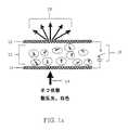
図1aに示すように、典型的なPDLCディスプレイには、少なくとも一方(10)は透明な(または透過性の)2枚の電極板(10、11)、および等方性ポリマーマトリックス中で分散した液晶ドメインの層が含まれる。また、図1aは、電圧(13)を2枚の電極板(10、11)に印加していない場合に液晶分子の方向がランダムなことを示す。よって、入射光(14)はランダムな向きの液晶分子によって散乱する(15)。Preferred Embodiments As shown in FIG. 1a, in a typical PDLC display, at least one (10) is transparent (or transmissive) two electrode plates (10, 11), and in an isotropic polymer matrix A layer of dispersed liquid crystal domains is included. FIG. 1a also shows that the orientation of the liquid crystal molecules is random when no voltage (13) is applied to the two electrode plates (10, 11). Therefore, incident light (14) is scattered by liquid crystal molecules in random directions (15).
図1bは、電圧(13)を2枚の電極板に印加した場合に液晶分子が所定の方向に向いていることを示す。よって、液晶の常光屈折率はポリマーマトリックス(12)の等方性の屈折率と整合するので、入射光(16)は透過する(17)。 FIG. 1b shows that the liquid crystal molecules are oriented in a predetermined direction when voltage (13) is applied to the two electrode plates. Thus, the normal light refractive index of the liquid crystal matches the isotropic refractive index of the polymer matrix (12), so that the incident light (16) is transmitted (17).
本発明のモノクロ液晶ディスプレイは、図1cに概略的に示すように、2枚の電極(10、11)間に閉じ込められ、適切に規定されたセル(18)を含む。このセル(18)は実質的に均一な形状および寸法を有し、LC組成物で充たされている。観者側にある電極は透明であり、2枚の電極の少なくとも一方はパターン形成されている。赤色(R)、緑色(G)および青色(B)などの三原色フィルターを用いる場合(図1d)、全範囲の色(フルカラー)を得ることができる。 The monochrome liquid crystal display of the present invention comprises a suitably defined cell (18) confined between two electrodes (10, 11), as schematically shown in FIG. 1c. This cell (18) has a substantially uniform shape and dimensions and is filled with an LC composition. The electrode on the viewer side is transparent, and at least one of the two electrodes is patterned. When three primary color filters such as red (R), green (G) and blue (B) are used (FIG. 1d), a full range of colors (full color) can be obtained.
別法では、本発明のフルカラーディスプレイは、R、GおよびBのゲスト染料、好ましくはそれぞれ二色性染料を含むLC組成物を、適切に規定せされたセル(1、2および3)に充填することによって得てよい。例えば、セル(1)は赤色ゲスト染料を有するLCで充填し、隣のセル(2)は緑色ゲスト染料を有するLCで充填し、および、隣のセル(3)は青色ゲスト染料を有するLCで充填する。LCを含有するセルの層の数は2以上であってよい(図1e)。 Alternatively, the full-color display of the present invention fills appropriately defined cells (1, 2 and 3) with LC compositions containing R, G and B guest dyes, preferably dichroic dyes, respectively. You may get it by doing For example, cell (1) is filled with LC with red guest dye, neighbor cell (2) is filled with LC with green guest dye, and neighbor cell (3) is LC with blue guest dye. Fill. The number of layers of cells containing LC may be 2 or more (FIG. 1e).
このようなLCディスプレイの製造方法にはいくつかの局面がある。 There are several aspects to the method of manufacturing such an LC display.
I.マイクロカップの製造
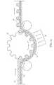
(a)雄型の製造
雄型は、フォトレジスト・プロセスおよびその後のエッチングまたは電気メッキによって製造できる。雄型の製造の代表的な例を図2a〜2dに示す。電気メッキを用いて(図2a)、ガラスベース(20)にクロムインコネルのようなシード・メタルの薄い層(21)(典型的には3000オングストローム)をスパッタ形成する。次に、フォトレジストの層(22)により被覆して、UVに曝露する。マスク(24)をUVとフォトレジストの層(22)との間に配置する。フォトレジストの露光領域は硬化状態となる。次に、非露光領域を適当な溶媒によって洗浄して除去する。残った硬化フォトレジストを乾燥し、シード・メタルの薄層を再びスパッタ形成する。このようにして電鋳用のマスター(図2b)が完成する。電鋳用の典型的な材料はニッケル・コバルト(23)である。別法では、マスターは、「コンティニュアス・マニュファクチャリング・オブ・シン・カバー・シート・オプティカル・メディア(Continuous manufacturing of thin cover sheet optical media)」(SPIE Proc.)第1663巻、第324頁(1992年)に記載されているように無電解ニッケル付着またはニッケルスルファメート電鋳によってニッケルにより形成してよい。型(図2d)のフロア(底部分)は典型的には1〜5ミクロンである。マスターは、e(電子)−ビーム・ライティング、ドライ・エッチング、ケミカル・エッチング、レーザー・ライティングまたはレーザー・インタフェアランス(laser interference)(例えば「リプリケーション・テクニクス・フォー・マイクロ−オプティックス(Replication techniques for micro-optics)」(SPIE Proc.)第3099巻、第76−82頁(1997年)に記載されているようなもの)を含む他のマイクロエンジニアリング技術を用いて形成することもできる。別法では、型は、プラスチック、セラミックまたは金属を用いるフォトマシニング(photomachining、光学的加工)によって形成できる。I. Manufacture of Microcups (a)Manufacture of male mold The male mold can be manufactured by a photoresist process followed by etching or electroplating. A representative example of male production is shown in FIGS. Using electroplating (FIG. 2a), a thin layer of seed metal (21) (typically 3000 angstroms) such as chrome inconel is sputtered onto the glass base (20). It is then covered with a layer of photoresist (22) and exposed to UV. A mask (24) is placed between the UV and the layer of photoresist (22). The exposed area of the photoresist is cured. Next, the non-exposed areas are removed by washing with an appropriate solvent. The remaining hardened photoresist is dried and a thin layer of seed metal is sputtered again. In this way, an electroforming master (FIG. 2b) is completed. A typical material for electroforming is nickel cobalt (23). Alternatively, the master may refer to “Continuous manufacturing of thin cover sheet optical media” (SPIE Proc.), 1663, p. 324. (1992) may be formed from nickel by electroless nickel deposition or nickel sulfamate electroforming. The floor (bottom part) of the mold (Figure 2d) is typically 1-5 microns. The master may be e (electron) -beam writing, dry etching, chemical etching, laser writing or laser interference (eg “Replication Techniques for Micro-Optics”). other microengineering techniques, including those described in Micro-optics) "(SPIE Proc.) 3099, 76-82 (1997)). Alternatively, the mold can be formed by photomachining using plastic, ceramic or metal.
(b)エンボス加工によるマイクロカップの製造
この処理工程を図3aおよび図3bに示す。雄型(30)は、ウェブ(34)の上方(図3a)または下方(図3b)に配置してよい。透明の導電性基材は、ガラスプレートまたはプラスチック基材上に透明の導体フィルム(31)を形成することによって作製する。そして、熱可塑性物または熱硬化物の前駆体(32)の層を導体フィルム上に被覆する。ローラー、プレートまたはベルトの形態の雄型により、熱可塑性物または熱硬化物の前駆体層のガラス転移温度より高い温度にて熱可塑性物または熱硬化物の前駆体層をエンボス加工する。(B) Production of microcups by embossing This process is shown in FIGS. 3a and 3b. The male mold (30) may be placed above (FIG. 3a) or below (FIG. 3b) the web (34). The transparent conductive substrate is produced by forming a transparent conductor film (31) on a glass plate or a plastic substrate. Then, a layer of the thermoplastic or thermoset precursor (32) is coated on the conductor film. The thermoplastic or thermoset precursor layer is embossed by a male mold in the form of a roller, plate or belt at a temperature above the glass transition temperature of the thermoplastic or thermoset precursor layer.
マイクロカップ(33)の製造に用いる熱可塑性物または熱硬化物の前駆体(32)は、多官能性のアクリレートまたはメタクリレート、ビニルエーテル、エポキシドおよびそのオリゴマー、ポリマー等であってよい。多官能性アクリレートおよびそのオリゴマーが最も好ましい。多官能性エポキシドおよび多官能性アクリレートの組み合わせも非常に有用であり、望ましい物理的−機械的性質を達成できる。エンボス加工したマイクロカップの耐屈曲性を向上させるために、可撓性を付与する架橋可能オリゴマー、例えばウレタンアクリレートまたはポリエステルアクリレートも通常加える。この組成物は、ポリマー、オリゴマー、モノマーおよび添加剤を含んでよく、あるいはオリゴマー、モノマーおよび添加剤のみを含んでよい。この種の材料のガラス転移温度(またはTg)は、通常、約−70℃〜約150℃、好ましくは約−20℃〜約50℃の範囲にある。マイクロエンボス加工処理は、典型的にはTgより高い温度で実施する。加熱した雄型または型を押し付ける加熱したハウジング基材を使用して、マイクロエンボス加工の温度および圧力を制御することができる。 The thermoplastic or thermoset precursor (32) used in the production of the microcup (33) may be a polyfunctional acrylate or methacrylate, vinyl ether, epoxide and its oligomer, polymer or the like. Most preferred are polyfunctional acrylates and oligomers thereof. Combinations of multifunctional epoxides and multifunctional acrylates are also very useful and can achieve desirable physical-mechanical properties. In order to improve the flex resistance of the embossed microcup, a crosslinkable oligomer that imparts flexibility, such as urethane acrylate or polyester acrylate, is also usually added. The composition may contain polymers, oligomers, monomers and additives, or may contain only oligomers, monomers and additives. The glass transition temperature (or Tg) of this type of material is usually in the range of about −70 ° C. to about 150 ° C., preferably about −20 ° C. to about 50 ° C. The microembossing process is typically performed at a temperature above Tg. A heated male mold or heated housing substrate that presses the mold can be used to control the temperature and pressure of microembossing.
図3aおよび図3bに示すように、前駆体層が硬化してマイクロカップ(33)のアレイを生じる間、またはその後、型を離す(またはリリースする)。前駆体層の硬化は、冷却、放射線、熱または湿気による架橋によって行うことができる。熱硬化物の前駆体の硬化をUV照射によって実施する場合、2つの図面に示すように、ウェブ(34)の下方からまたは上方から透明導体フィルムにUVを照射してよい。別法では、型の内部にUVランプを配置してよい。この場合、型は予めパターン形成した雄型を通して熱硬化物の前駆体層にUV光を照射できるように透明である必要がある。 As shown in FIGS. 3a and 3b, the mold is released (or released) during or after the precursor layer cures to produce an array of microcups (33). Curing of the precursor layer can be performed by crosslinking with cooling, radiation, heat or moisture. When curing of the precursor of the thermoset is carried out by UV irradiation, the transparent conductor film may be irradiated with UV from below or above the web (34) as shown in the two drawings. Alternatively, a UV lamp may be placed inside the mold. In this case, the mold needs to be transparent so that the thermoset precursor layer can be irradiated with UV light through a previously patterned male mold.
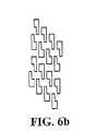
図4aおよび4bはマイクロエンボス加工によって製造した2種のマイクロカップアレイのSEM写真を示す。 4a and 4b show SEM photographs of two microcup arrays produced by microembossing.
(c)画像露光によるマイクロカップの製造
別法では、導体フィルム(52)上に被覆した放射線硬化性材料(51)をUVまたは他の形態の放射線にマスク(50)を介して画像露光する(図5a)ことにより、マイクロカップを形成できる。導体フィルム(52)は、プラスチック基材(53)上に存在する。(C) Manufacture of microcups by image exposure Alternatively, the radiation curable material (51) coated on the conductor film (52) is image exposed to UV or other forms of radiation through a mask (50) ( 5a), a microcup can be formed. The conductor film (52) exists on the plastic substrate (53).
ロール・トゥ・ロール・プロセスの場合、フォトマスクをウェブと同調させてウェブと同じスピードで移動させてよい。図5aのフォトマスク(50)において、暗い方形部(54)は、不透明な領域を示し、暗い方形部の間の空間(55)は、光が通過する領域を示す。UVは光が通過する領域(55)を通って放射線硬化性材料に達する。露光した領域は硬化し、その後、露光されない領域(マスクの不透明な領域により保護されている)は、適当な溶媒または現像液により除去してマイクロカップ(56)を形成する。溶媒または現像液は、放射線硬化性材料を溶解または分散させるために一般的に使用されているもの、例えばメチルエチルケトン、トルエン、アセトン、イソプロパノール等から選択される。 In the case of a roll-to-roll process, the photomask may be moved at the same speed as the web in sync with the web. In the photomask (50) of FIG. 5a, dark squares (54) indicate opaque regions, and spaces (55) between dark squares indicate regions through which light passes. UV reaches the radiation curable material through the region (55) through which light passes. The exposed areas are cured and then the unexposed areas (protected by the opaque areas of the mask) are removed with a suitable solvent or developer to form the microcup (56). The solvent or developer is selected from those commonly used to dissolve or disperse radiation curable materials, such as methyl ethyl ketone, toluene, acetone, isopropanol, and the like.
図5bおよび図5cは、画像露光によりマイクロカップを形成する2つの他のオプションを示す。これらの2つの図面における特徴は、図5aと本質的に同じであり、対応する部分は、同じ番号を付している。図5bにおいて、使用する導体フィルム(52)は、不透明であり、予めパターン形成されている。この場合、フォトマスクとして機能する導体パターンを介して放射線感応性材料を画像露光することが有利で有り得る。その後、UV照射後に非露光領域を除去することによってマイクロカップ(56)を形成できる。図5cにおいて、導体フィルム(52)は、不透明であり、ラインのパターンが形成されている。第1のフォトマスクとして作用する導体ラインパターン(52)を介して放射線硬化性材料をその底部から露光する。導体ラインに対して垂直なラインパターンを有する第2のフォトマスク(50)を介して他方側から第2の露光を実施する。その後、非露光領域を溶媒または現像液により除去すると、マイクロカップ(56)が現れる。 Figures 5b and 5c show two other options for forming microcups by image exposure. The features in these two figures are essentially the same as in FIG. 5a, and corresponding parts are given the same numbers. In FIG. 5b, the conductor film (52) used is opaque and pre-patterned. In this case, it may be advantageous to image expose the radiation sensitive material through a conductor pattern that functions as a photomask. Thereafter, the microcup (56) can be formed by removing the non-exposed areas after UV irradiation. In FIG. 5c, the conductor film (52) is opaque and has a pattern of lines. The radiation curable material is exposed from its bottom through a conductor line pattern (52) that acts as a first photomask. Second exposure is performed from the other side through a second photomask (50) having a line pattern perpendicular to the conductor lines. Thereafter, when the non-exposed area is removed with a solvent or developer, a microcup (56) appears.
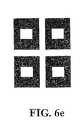
一般的に、マイクロカップ(56)は液晶ドメインの光散乱効果を最大限にするようにいずれの形態であってもよい。1つのシステムにおいて、マイクロカップは、実質的に一様な寸法および形状である。しかしながら、異なる形状および寸法を有するマイクロカップを異なる色に対して用いてもよい。例えば、赤色のゲスト染料を有するLCを充填したマイクロカップは、緑色のマイクロカップまたは青色のマイクロカップと異なる形状および寸法を有してよい。更に、ピクセルは、異なる色の異なる数のマイクロカップから成ってよい。また、ピクセルは、幾つかの小さい緑色マイクロカップ、幾つかの大きい赤色マイクロカップおよび幾つかの小さい青色マイクロカップから成ってもよい。3つの色に対して同じ形状および数とする必要は必ずしもない。図6a〜6fは本発明において使用され得るマイクロカップパターンの6つの例を示す。 In general, the microcup (56) may be in any form to maximize the light scattering effect of the liquid crystal domain. In one system, the microcups are substantially uniform in size and shape. However, microcups having different shapes and dimensions may be used for different colors. For example, a microcup filled with LC with a red guest dye may have a different shape and size than a green or blue microcup. Furthermore, the pixels may consist of different numbers of microcups of different colors. The pixel may also consist of several small green microcups, several large red microcups and several small blue microcups. The same shape and number are not necessarily required for the three colors. Figures 6a-6f show six examples of microcup patterns that can be used in the present invention.
マイクロカップの開口部は、円形(または丸い形状)、正方形、矩形、六角形または他のいずれかの形状であってよい。開口部の間の仕切領域は、望ましい機械的性質を維持しながらも、大きい彩度およびコントラスト比を達成するために小さく維持することが好ましい。 The opening of the microcup may be circular (or round), square, rectangular, hexagonal or any other shape. The partition area between the openings is preferably kept small to achieve a high saturation and contrast ratio while maintaining the desired mechanical properties.
本発明のLCディスプレイの場合、各々の個々のマイクロカップのディメンションは、約0.04〜約100μm2、好ましくは約0.6μm2〜約36μm2の範囲であり得る。マイクロカップの深さは、約1〜約10ミクロン、好ましくは約2〜約6ミクロンの範囲である。開口部の壁に対する割合は、約0.05〜約20、好ましくは約0.2〜約10の範囲内にある。開口部の距離は、開口部のエッジからエッジまでで通常は約0.5〜約6ミクロン、好ましくは約1〜約4ミクロンである。For LC display of the present invention, each of the dimensions of the individual microcups, about 0.04 to about 100 [mu] m2, preferably it can range from about 0.6 .mu.m2 ~ about 36 .mu.m2. The depth of the microcup ranges from about 1 to about 10 microns, preferably from about 2 to about 6 microns. The ratio of opening to wall is in the range of about 0.05 to about 20, preferably about 0.2 to about 10. The distance of the opening is usually from about 0.5 to about 6 microns, preferably from about 1 to about 4 microns from edge to edge of the opening.
II.液晶、二色性染料およびそれらの混合物
以上のようにして製造したマイクロカップのアレイに液晶を、通常はコーティング法によって充填する。ディスプレイにモノクロの色を付与し、また、コントラストを増大させるため、液晶は二色性染料も含み得る。II.Liquid crystals, dichroic dyes and mixtures thereof Liquid crystals are filled into an array of microcups prepared as described above, usually by a coating method. To impart a monochrome color to the display and to increase contrast, the liquid crystal may also contain a dichroic dye.
本発明において使用され得る液晶材料は当該技術分野において周知である。本発明において使用され得る液晶材料の例には、E7、TL205、TL213、BL006およびBL037(イー・メルク社(E. Merck Co.)製、ドイツ)があるが、これに限定されない。また、他の液晶材料も米国特許第5,835,174号(Clikemanら)に列挙されている。また、コレステリック液晶も同じ用途に使用してよい。 Liquid crystal materials that can be used in the present invention are well known in the art. Examples of liquid crystal materials that can be used in the present invention include, but are not limited to, E7, TL205, TL213, BL006, and BL037 (E. Merck Co., Germany). Other liquid crystal materials are also listed in US Pat. No. 5,835,174 (Clikeman et al.). Cholesteric liquid crystals may also be used for the same purpose.
本発明において液晶は好ましくはゲスト染料を含む。本発明のゲスト染料は二色性であり、当該技術分野において周知である。米国特許第5,589,100号を参照でき、これには、アリールアゾまたはポリ(アリールアゾ)二色性染料を液晶と一緒に使用できることが述べられており、また、本発明に適する他の二色性染料が列挙されている。 In the present invention, the liquid crystal preferably contains a guest dye. The guest dyes of the present invention are dichroic and are well known in the art. Reference may be made to US Pat. No. 5,589,100, which mentions that arylazo or poly (arylazo) dichroic dyes can be used with liquid crystals, and other dichroic colors suitable for the present invention. Sex dyes are listed.
染料を混ぜることによって、着色するだけでなく、いくつかのディスプレイ用途においてコントラストを実質的に向上させることもできる。適切には、染料は高い配向パラメータおよびホスト液晶材料中での適当な溶解度を有していなければならない。高い配向パラメータは、液晶ホスト材料の分子の形状と同様、分子長さ対幅の割合の大きな細長い形状を有する染料によって助長される。ゲスト染料を有するLCは、例えば高コントラスト、高消光度ならびに化学的および光化学的安定性などの良好な視野特性を提供するであろう。本発明において使用する高い二色比を有する二色性染料の例にはブルーAB2、レッドAR1およびイェローAG1(フンクチオンフルイド社(Funktionfluid GmbH)製、ドイツ)ならびにSI−486(黄色)、SI426(赤色)、M483(青色)、S344(黒色)、S428(黒色)およびS7(黒色)(三井東圧社製)がある。 Mixing dyes can not only color, but can also substantially improve contrast in some display applications. Suitably the dye should have high orientation parameters and suitable solubility in the host liquid crystal material. The high orientation parameter is facilitated by a dye having an elongated shape with a large ratio of molecular length to width, similar to the molecular shape of the liquid crystal host material. LCs with guest dyes will provide good viewing properties such as high contrast, high extinction and chemical and photochemical stability. Examples of dichroic dyes having a high dichroic ratio used in the present invention include Blue AB2, Red AR1 and Yellow AG1 (Funktionfluid GmbH, Germany) and SI-486 (yellow), SI426 ( Red), M483 (blue), S344 (black), S428 (black) and S7 (black) (Mitsui Toatsu).
また、ノニオン性アゾおよびアントラキノン染料も有用である。有用な染料の例には次のものが含まれるが、それらに限定されるものではない:オイル・レッド(Oil Red)EGN、スーダン・レッド(Sudan Red)、スーダン・ブルー(Sudan Blue)、オイル・ブルー(Oil Blue)、マクロレックス・ブルー(Macrolex Blue)、ソルベント・ブルー(Solvent Blue)35、ピラム・スピリット・ブラック(Pylam Spirit Black)およびファスト・スピリット・ブラック(Fast Spirit Black)(ピラム・プロダクツ(Pylam Products)社(アリゾナ)製)、スーダン・ブラック(Sudan Black)B(アルドリッチ(Aldrich)製)、サーモプラスチック・ブラック(Thermoplastic Black)X−70(バスフ(BASF)製)、アントロキノン・ブルー(anthroquinone blue)、アントロキノン・イェロー(anthroquinone yellow)114、アントロキノン・レッド(anthroquinone red)111、135、アントロキノン・グリーン(anthroquinone green)28(アルドリッチ製)。いずれにせよ、染料または色素は化学的に安定でなければならず、マイクロカップ材料中において低い溶解度を有する必要がある。液晶または染料は、どのような場合もマイクロカップを攻撃してはならない。 Nonionic azo and anthraquinone dyes are also useful. Examples of useful dyes include, but are not limited to: Oil Red EGN, Sudan Red, Sudan Blue, oil・ Oil Blue, Macrolex Blue, Solvent Blue 35, Pylam Spirit Black and Fast Spirit Black (Piram Products) (Pylam Products) (Arizona), Sudan Black B (Aldrich), Thermoplastic Black X-70 (Basf (BASF)), Antroquinone Blue (Anthroquinone blue), anthroquinone yellow 114, anthroquinone red 11,135, anthroquinones Green (anthroquinone green) 28 (Aldrich). In any case, the dye or pigment must be chemically stable and have a low solubility in the microcup material. Liquid crystals or dyes should in no case attack the microcups.
III.マイクロカップのシーリング
マイクロカップのシーリング(または封止)は、幾つかの方法で実施できる。好ましい方法は、UV硬化性封止組成物をLC組成物中に分散させる方法である。UV硬化性組成物はLCと非混和性であり、LCより小さい比重を有する。UV硬化性組成物およびLC組成物をインラインミキサーで十分にブレンドして、精密なコーティング機構、例えばマイラド・バー(Myrad bar)、グラビア印刷、ドクター・ブレード、スロット・コーティングまたはスリット・コーティングによってマイクロカップ上に直ちに被覆する。揮発性溶媒を使用して粘度およびコーティングの被覆率(coverage)を制御し、LC相からの封止剤相の分離を容易にしてよい。ワイパーブレードまたは同様のデバイスを用いて過剰の流体を掻きとって除去してよい。このようにして充填したマイクロカップを乾燥すると、UV硬化性組成物はLCの上部に浮かんでくる。それが上に浮かんでくる間またはその後、上澄部のUV硬化性層を硬化することによってマイクロカップを封止できる。UVまたは他の形態の放射線、例えば可視光、IRおよび電子線ビームを使用して硬化してマイクロカップをシールしてもよい。別法では、熱または湿気硬化性封止組成物を用いる場合には、熱または湿気あるいはそれらの組合せを利用して硬化してマイクロカップをシールしてもよい。III.Microcups sealing the microcups sealing (or sealing) can be carried out in several ways. A preferred method is to disperse the UV curable sealing composition in the LC composition. UV curable compositions are immiscible with LC and have a specific gravity less than LC. The UV curable composition and the LC composition are thoroughly blended in an in-line mixer to produce microcups with precision coating mechanisms such as Myrad bar, gravure printing, doctor blade, slot coating or slit coating. Immediately coat on. Volatile solvents may be used to control viscosity and coating coverage to facilitate separation of the sealant phase from the LC phase. Excess fluid may be scraped off using a wiper blade or similar device. When the filled microcups are dried, the UV curable composition floats on top of the LC. The microcup can be sealed by curing the UV curable layer in the supernatant while it floats up or afterwards. The microcups may be sealed by curing using UV or other forms of radiation, such as visible light, IR and electron beam. Alternatively, if a heat or moisture curable sealing composition is used, the microcups may be sealed by curing using heat or moisture or a combination thereof.
界面活性剤を使用して、マイクロカップ壁への封止剤の付着およびLCとシーリング物質との間の界面における濡れを改善することができる。有用な界面活性剤には、FC界面活性剤(3M社製)、ゾニル(Zonyl)フルオロ界面活性剤(デュポン製)、フルオロアクリレート、フルオロメタクリレート、フッ素置換長鎖アルコール、パーフルオロ置換長鎖カルボン酸およびそれらの誘導体、ならびにシルウェット(Silwet)界面活性剤(OSi製)が含まれる。 Surfactants can be used to improve sealant adhesion to the microcup wall and wetting at the interface between the LC and the sealing material. Useful surfactants include FC surfactants (manufactured by 3M), Zonyl fluorosurfactants (manufactured by DuPont), fluoroacrylates, fluoromethacrylates, fluorine-substituted long-chain alcohols, perfluoro-substituted long-chain carboxylic acids. And their derivatives, as well as Silwet surfactants (made by OSi).
別法では、LCおよび封止組成物をマイクロカップ内に順に被覆してもよい。従って、マイクロカップのシーリングは、放射線、熱、湿気または界面反応によって硬化する熱可塑性物または熱硬化物の前駆体組成物の薄層をオーバーコートし、充填したマイクロカップの表面で硬化することによって行うことができる。界面重合およびその後のUV硬化は、シーリング方法に非常に有用である。LC層とオーバーコートとの間の混合は、界面重合によって界面に薄いバリヤー層を形成することによって相当抑制できる。その後、好ましくはUV照射による、後硬化工程によってシーリングが完了する。混合を更に減らすために、オーバーコートの比重がLCの比重より小さいことが非常に望ましい。揮発性有機溶媒を使用して、コーティングの粘度および厚さを調節することができる。揮発性溶媒をオーバーコートにて使用する場合、揮発性溶媒はLCまたは染料と非混和性であり、LC相の比重より小さい比重を有することが好ましい。使用する染料が封止剤層において少なくとも部分的に溶解する場合、2段階オーバーコートプロセスが特に有用である。封止剤層とLC層との間の混合を更に減らすために、封止剤層のオーバーコーティングの前に、充填したマイクロカップアレイを冷却してよい。 Alternatively, the LC and sealing composition may be sequentially coated in the microcup. Therefore, microcup sealing is achieved by overcoating a thin layer of thermoplastic or thermoset precursor composition that cures by radiation, heat, moisture or interfacial reaction and curing on the surface of the filled microcup. It can be carried out. Interfacial polymerization and subsequent UV curing is very useful for sealing methods. Mixing between the LC layer and the overcoat can be significantly suppressed by forming a thin barrier layer at the interface by interfacial polymerization. Thereafter, the sealing is completed by a post-curing step, preferably by UV irradiation. In order to further reduce mixing, it is highly desirable that the specific gravity of the overcoat be less than the specific gravity of the LC. Volatile organic solvents can be used to adjust the viscosity and thickness of the coating. When a volatile solvent is used in the overcoat, the volatile solvent is preferably immiscible with the LC or dye and has a specific gravity less than the specific gravity of the LC phase. A two-stage overcoat process is particularly useful when the dye used is at least partially dissolved in the encapsulant layer. To further reduce mixing between the sealant layer and the LC layer, the filled microcup array may be cooled prior to the overcoat of the sealant layer.
別法では、充填したマイクロカップのシーリングは、接着剤層をリリース基板から充填したマイクロカップに転写ラミネートし、好ましくはその後、熱、放射線によってまたは単に溶媒蒸発によって接着剤層を硬化させ、リリース基板を最後に剥離することによって行うことができる。転写ラミネートプロセスによるシーリングにおいても、充填したマイクロカップを冷却することは有用である。 Alternatively, the sealing of the filled microcup can be accomplished by transfer laminating the adhesive layer from the release substrate to the filled microcup, and then preferably curing the adhesive layer by heat, radiation or simply by solvent evaporation, Can be performed by finally peeling. It is also useful to cool the filled microcups in sealing by a transfer laminating process.
IV.モノクロLCディスプレイの製造
このプロセスを図7に示すようなフローダイアグラムによって説明する。同じ色の組成物のゲスト染料を含むLCによって全てのマイクロカップを充填する。このプロセスは、以下の工程を含んで成る連続的なロール・トゥ・ロール・プロセスとすることができる:
1.透明導体フィルム(71)上に適宜溶媒を含む熱可塑性物または熱硬化物の前駆体の層(70)をコートする。溶媒は存在する場合には容易に蒸発する。
2.予めパターン形成した雄型(72)によって、熱可塑性物または熱硬化物の前駆体層のガラス転移温度より高い温度にて熱可塑性物または熱硬化物の前駆体層をエンボス加工する。
3.熱可塑性物または熱硬化物の前駆体層を適当な手段によって硬化する好ましくはその間またはその後、その層から型を離す。
4.LCと非相溶性であり、LC相より小さい比重を有する熱硬化物の前駆体を含むLC組成物(74)を上述のように形成したマイクロカップ(73)のアレイに充填する。
5.熱硬化物の前駆体が分離してLC相の上部に上澄相を形成する間またはその後、好ましくは溶媒蒸発、UV(75)のような放射線によって、または熱もしくは湿気によって、熱硬化物の前駆体を硬化させることによってマイクロカップをシールし、そのようにして、LCおよび好ましくはゲスト染料を含む閉じたLCセルを形成する。
6.感圧接着剤、ホットメルト接着剤、熱、湿気または放射線硬化性接着剤であってよい接着剤層(77)を予め被覆した第2導体フィルム(76)によってLCセルのシールしたアレイをラミネートする。IV.Manufacturing Monochrome LC Display This process is illustrated by a flow diagram as shown in FIG. All microcups are filled with LC containing a guest dye of the same color composition. This process can be a continuous roll-to-roll process comprising the following steps:
1. The transparent conductor film (71) is coated with a thermoplastic or thermoset precursor layer (70) containing a solvent as appropriate. Solvents readily evaporate when present.
2. The pre-patterned male mold (72) embosses the thermoplastic or thermoset precursor layer at a temperature above the glass transition temperature of the thermoplastic or thermoset precursor layer.
3. The thermoplastic or thermoset precursor layer is cured by suitable means, preferably during or after the mold is released from the layer.
4). An LC composition (74) comprising a thermoset precursor that is incompatible with LC and has a specific gravity less than the LC phase is loaded into an array of microcups (73) formed as described above.
5). During or after the precursor of the thermoset separates and forms a supernatant phase on top of the LC phase, preferably by solvent evaporation, radiation such as UV (75), or by heat or moisture, The microcups are sealed by curing the precursor, thus forming a closed LC cell containing LC and preferably a guest dye.
6). Laminate a sealed array of LC cells with a second conductor film (76) pre-coated with an adhesive layer (77), which may be a pressure sensitive adhesive, hot melt adhesive, heat, moisture or radiation curable adhesive. .
ラミネートの接着剤は、熱によって、または、上部の導体フィルムが放射線に対して透明である場合には、それを介してUV(78)のような放射線によって硬化させてよい。ラミネートしたプロダクトをデバイスの組立てに適当な寸法に切断してよい(79)。 The laminate adhesive may be cured by heat or by radiation such as UV (78) through the top conductor film if it is transparent to the radiation. The laminated product may be cut to dimensions appropriate for device assembly (79).
上述のマイクロカップの形成は、熱硬化物の前駆体(より詳細には放射線硬化性組成物)を被覆した導体フィルムを画像露光し、その後、非露光領域を適当な溶媒によって除去する別の方法によって置換するのが好都合である場合がある。別法では、マイクロカップのシールは、上述のオーバーコートまたは転写ラミネートプロセスにより、その後、充填したマイクロカップの表面で封止剤を硬化させることによって行ってもよい。 The formation of the microcups described above is another method in which a conductor film coated with a thermoset precursor (more specifically, a radiation curable composition) is image-exposed and then the unexposed areas are removed with a suitable solvent. It may be convenient to substitute by: Alternatively, microcup sealing may be performed by the overcoat or transfer lamination process described above, followed by curing of the sealant on the filled microcup surface.
コントラスト比を改善するために、マイクロカップアレイのより多くの層を用いることができる(図1c)。よって、充填したマイクロカップの上で封止剤層を硬化させた後(工程5)、シールしたマイクロカップアレイの上に、マイクロカップを形成する組成物の別の層をコートする。適当なコントラスト比が得られるまで工程2〜5を何度か繰り返す。その後、多層マイクロカップスタック(または積層体)を第2の導体層でラミネートし、ディスプレイの組立てに適当な寸法に切断する。2つの導体フィルムの少なくとも一方を予めパターン形成することに留意するのが重要である。また、少なくとも観者側にある導体フィルムは透明である。 More layers of the microcup array can be used to improve the contrast ratio (FIG. 1c). Thus, after curing the sealant layer on the filled microcups (step 5), another layer of the composition forming the microcups is coated on the sealed microcup array. Steps 2-5 are repeated several times until a suitable contrast ratio is obtained. The multilayer microcup stack (or stack) is then laminated with a second conductor layer and cut to dimensions appropriate for display assembly. It is important to note that at least one of the two conductor films is pre-patterned. Also, at least the conductor film on the viewer side is transparent.
V.マルチカラーLCディスプレイの製造
本発明のマルチカラーLCディスプレイは、前節にて製造したモノクロディスプレイの下方に位置する(R、G、B)カラーフィルターおよびブラックマトリックスを用いることによって製造できる(図1d)。あるいは、本発明のフルカラーディスプレイは、異なる色のゲスト染料を含むLCをマイクロカップに充填することによって製造できる(図1e)。このようなカラーディスプレイには、モノクロディスプレイの製造にて説明したプロセスに加えて追加の工程が必要である。これらの追加の工程には次のものが含まれる:
(1)除去可能支持体、例えばPET−4851(セント−ゴベイン(Saint-Gobain)製、マサチューセッツ州ウスター)、ノボラックポジ型フォトレジスト、例えばマイクロポジット(Microposit)S1818(シップレイ(Shipley)製)およびアルカリ現像可能な(alkali-developable)接着剤層、例えばナコー(Nacor)72−8685(ナショナル・スターチ(National Starch)製)およびカーボセット(Carboset)515(BFグッドリッチ(Goodrich)製)の混合物から少なくとも成るポジ型ドライフィルムフォトレジストを、既に形成したマイクロカップに積層すること、
(2)フォトレジストの画像露光によって、ある数のマイクロカップを選択的に開口し、除去可能支持体フィルムを除去し、現像液、例えば希釈したマイクロポジット351現像液(シップレイ製)によってポジ型フォトレジストを現像すること、
(3)第1原色のゲスト染料を有するLCを開いたカップに充填すること、および
(4)モノクロディスプレイの製造にて説明したように、充填したマイクロカップをシールすること。
これらの追加の工程を繰り返して第2および第3の原色のLCを充填したマイクロカップを形成する。V.Manufacture of Multicolor LC Display The multicolor LC display of the present invention can be manufactured by using (R, G, B) color filters and a black matrix located below the monochrome display manufactured in the previous section (FIG. 1d). Alternatively, the full color display of the present invention can be produced by filling LCs containing guest dyes of different colors into microcups (FIG. 1e). Such color displays require additional steps in addition to the processes described in the manufacture of monochrome displays. These additional steps include the following:
(1) Removable supports such as PET-4851 (from Saint-Gobain, Worcester, Mass.), Novolac positive photoresists such as Microposit S1818 (from Shipley) and alkalis At least from a mixture of an alkali-developable adhesive layer, such as Nacor 72-885 (from National Starch) and Carboset 515 (from BF Goodrich) Laminating a positive dry film photoresist consisting of microcups already formed,
(2) A certain number of microcups are selectively opened by image exposure of the photoresist, the removable support film is removed, and a positive type photo is developed with a developer, for example, a diluted microposit 351 developer (Shipley). Developing the resist,
(3) Filling the open cup with the LC having the first primary color guest dye, and (4) Sealing the filled microcup as described in the manufacture of the monochrome display.
These additional steps are repeated to form microcups filled with LC of the second and third primary colors.
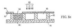
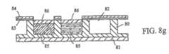
より詳しくは、マルチカラーLCディスプレイは、図8に示すような工程に基づいて製造できる:
1.導体フィルム(81)上に熱可塑性物または熱硬化物の前駆体の層(80)を被覆する。
2.予めパターン形成した雄型(図示せず)によって熱可塑性物または熱硬化物の前駆体層のガラス転移温度より高い温度にてその層をエンボス加工する。
3.好ましくは、溶媒蒸発、冷却あるいは放射線、熱または湿気による架橋によって熱可塑性物または熱硬化物の前駆体層が硬化する間、またはその後、熱可塑性物または熱硬化物の前駆体層から型を外す。
4.少なくともポジ型フォトレジスト(84)および除去可能プラスチックカバーシート(図示せず)を有して成るポジ型ドライフィルムフォトレジストをそのように形成したマイクロカップ(82)のアレイに積層する。マイクロカップとレジストとの間の付着を改善するため、ポジ型ドライフィルムフォトレジストは接着剤層(83)を含んでいてよい。
5.UV、可視光、または他の放射線によってポジ型フォトレジストを画像露光し(図8c)、カバーシートを除去し、現像して露光領域においてカップを開く。工程4および5の目的は、所定領域においてマイクロカップを選択的に開くことである(図8d)。
6.開いたマイクロカップに、第1の原色のゲスト染料(85)を含むLC組成物および封止組成物(86)(LC相と非相溶性であり、LC相より小さい比重を有する)を充填する。
7.封止剤が分離して液晶相の上部に上澄相を形成する(図8e)間またはその後、封止剤層を溶媒蒸発によって硬化させることによって、または好ましくは放射線、例えばUVによって、好ましさが劣るが、熱または湿気によって硬化させることによってマイクロカップをシールして、第1の原色のゲスト染料を有するLCを含む、閉じたLCセルを形成する。
8.上述の工程5〜7を繰り返して、異なる領域に異なる色のゲスト染料を有するLCを含む、適切に規定されたセルを形成してよい(図8e、図8fおよび図8g)。
9.第2の透明導体フィルム(87)(感圧接着剤、ホットメルト接着剤、熱、湿気または放射線硬化性接着剤であってよい接着剤層(88)を予め被覆してある)に対してLCセルのシールしたアレイをラミネートする。
10.接着剤を硬化させる。More specifically, a multi-color LC display can be manufactured based on a process as shown in FIG.
1. The conductor film (81) is coated with a thermoplastic or thermoset precursor layer (80).
2. The layer is embossed at a temperature above the glass transition temperature of the thermoplastic or thermoset precursor layer with a pre-patterned male mold (not shown).
3. Preferably, the mold is removed from the thermoplastic or thermoset precursor layer during or after curing of the thermoplastic or thermoset precursor layer by solvent evaporation, cooling or crosslinking by radiation, heat or moisture. .
4). A positive dry film photoresist comprising at least a positive photoresist (84) and a removable plastic cover sheet (not shown) is laminated to the array of microcups (82) so formed. To improve adhesion between the microcup and the resist, the positive dry film photoresist may include an adhesive layer (83).
5). The positive photoresist is image exposed with UV, visible light, or other radiation (FIG. 8c), the cover sheet is removed and developed to open the cup in the exposed area. The purpose of steps 4 and 5 is to selectively open the microcups in a predetermined area (FIG. 8d).
6). An open microcup is filled with an LC composition comprising a first primary color guest dye (85) and a sealing composition (86) (incompatible with the LC phase and having a specific gravity less than the LC phase). .
7). During or after the sealant separates to form a supernatant phase on top of the liquid crystal phase (FIG. 8e) or afterwards, preferably by curing the sealant layer by solvent evaporation or preferably by radiation, eg UV. Less well, but the microcups are sealed by curing with heat or moisture to form a closed LC cell containing LC with a first primary color guest dye.
8). Steps 5-7 described above may be repeated to form appropriately defined cells containing LCs with different colored guest dyes in different regions (FIGS. 8e, 8f and 8g).
9. LC against second transparent conductor film (87) (pre-coated with adhesive layer (88), which may be a pressure sensitive adhesive, hot melt adhesive, heat, moisture or radiation curable adhesive) Laminate the sealed array of cells.
10. Allow the adhesive to cure.
上述のプロセスにおいて説明したマイクロカップの形成は、熱硬化物の前駆体(より詳細には放射線硬化性組成物)を被覆した導体フィルムを画像露光し、その後、非露光領域を適当な溶媒によって除去する別の方法によって置換するのが好都合である場合がある。別法では、マイクロカップのシールは、熱硬化物の前駆体物質の層を液相の表面の上に直接被覆することによって行ってもよい。 The formation of the microcups described in the above process involves image exposure of a conductor film coated with a thermoset precursor (more specifically, a radiation curable composition) and then removing the unexposed areas with a suitable solvent. It may be convenient to substitute by another method. Alternatively, microcup sealing may be accomplished by coating a layer of thermoset precursor material directly on the surface of the liquid phase.
説明した本発明の方法によって製造されるディスプレイの厚さは、1枚の紙のように薄くすることができる。ディスプレイの幅は、被覆ウェブの幅(典型的には3〜90インチ)である。ディプレイの長さは、ロールのサイズに応じて、数インチから何千フィートのいずれにもすることができる。 The thickness of the display produced by the described method of the invention can be as thin as a piece of paper. The width of the display is the width of the coated web (typically 3 to 90 inches). The display length can be anywhere from a few inches to thousands of feet, depending on the size of the roll.
当業者が本発明をより明確に理解して実施できるように、以下に実施例を説明する。これらは、本発明の範囲を制限するものと理解すべきではなく、単に、本発明を例示して代表するものであると理解すべきである。 The following examples are provided to enable those skilled in the art to more clearly understand and to practice the present invention. They should not be understood as limiting the scope of the invention, but merely as exemplifying and representative of the invention.
実施例1
マイクロエンボス加工によるマイクロカップの形成
ITO導体層を予めコートした2ミル(mil)PETフィルム(シェルダール(Sheldahl)製、ノースフィールド、ミネソタ)上に表1に示す組成物をマイラド・バー#6で被覆した。予めパターン形成(4×4×4ミクロン)したコバルト・ニッケル雄型および離型剤フレコート(Frekote)700−NC(ヘンケル製)をマイクロエンボス加工に用いた。コーティングの厚さは約5ミクロンに制御した。その後、加圧ローラーを90℃にて用いてステンシルによって、被覆したフィルムをエンボス加工した。その後、365nmで80mW/cm2の強度を有する金属フッ化物ランプを備えるキュアゾーン(Cure Zone)露光装置(ADACテクノロジーズ(ADAC Technologies)社製)を用いて、マイラー(Mylar)フィルムを介して約1分間に亘ってコーティングをUV硬化させた。その後、エンボス加工したフィルムを型から離し、適切に規定された(4×4×4ミクロン)マイクロカップを顕在化させた。このマイクロエンボス加工はGBCラミネーターを90℃にて用いて実施した。Example 1
Formation of microcups by microembossing The composition shown in Table 1 on a 2 mil PET film (manufactured by Sheldahl, Minnesota) pre-coated with an ITO conductor layer is obtained using Myrad Bar # 6. Covered. Pre-patterned (4 × 4 × 4 microns) cobalt nickel male mold and release agent Frekote 700-NC (Henkel) were used for microembossing. The coating thickness was controlled at about 5 microns. The coated film was then embossed with a stencil using a pressure roller at 90 ° C. After that, using a Cure Zone exposure apparatus (manufactured by ADAC Technologies) equipped with a metal fluoride lamp having an intensity of 80 mW / cm2 at 365 nm, about 1 through Mylar film. The coating was UV cured for a minute. The embossed film was then removed from the mold and a well-defined (4 × 4 × 4 micron) microcup was revealed. This microembossing was performed using a GBC laminator at 90 ° C.

実施例2
マイクロエンボス加工によるマイクロカップの形成
表2に示す調製物を被覆して4×4×4ミクロンの雄型でエンボス加工したこと以外は実施例1と同じに実施した。Example 2
Formation of microcups by microembossing The same procedure as in Example 1 was followed, except that the preparation shown in Table 2 was coated and embossed with a 4 × 4 × 4 micron male mold.
マイラド・バー#12を用いた。制御厚さは5ミクロンとした。マイクロエンボス加工は90℃に加熱した加圧ローラー(GBCラミネーター)を用いて実施した。
実施例3
マイクロエンボス加工によるマイクロカップの形成
ITO導体層を予めコートした2ミル(mil)PETフィルムと予めパターン形成(4×4×4ミクロン)したコバルト・ニッケル型との間に表3に示す組成物を、加圧ローラーを用いてラミネートした。PFT/ITOフィルムをコロナ放電(エレクトロ−テクニックプロダクツ(Electro-Technic Products)製、モデルBD−10A、シカゴ、イリノイ)により5秒間処理した。コバルト・ニッケル型は離型剤フレコート750−NCで前処理した。その後、PET/ITOフィルムを介して約1分間に亘ってコーティングをUV硬化させた。その後、エンボス加工したフィルムを型から離し、適切に規定された(4×4×4ミクロン)マイクロカップ(ミツトヨ厚さゲージによる測定で5.5ミクロンの厚さを有する)を顕在化させた。Example 3
Formation of microcups by microembossing The composition shown in Table 3 is placed between a 2 mil PET film pre-coated with an ITO conductor layer and a cobalt-nickel mold pre-patterned (4 × 4 × 4 microns). Lamination was performed using a pressure roller. The PFT / ITO film was treated with corona discharge (manufactured by Electro-Technic Products, model BD-10A, Chicago, Illinois) for 5 seconds. The cobalt-nickel mold was pretreated with a release agent Frecoat 750-NC. The coating was then UV cured through a PET / ITO film for about 1 minute. The embossed film was then removed from the mold and a well-defined (4 × 4 × 4 micron) microcup (having a thickness of 5.5 microns as measured by Mitutoyo thickness gauge) was revealed.
実施例4
液晶溶液を充填したマイクロカップの形成
実施例3で形成したマイクロカップをヘキサンで、その後にMEKで洗浄し、そしてオーブン(66℃)で10分間乾燥させた。1重量%のシルウェット(Silwet)L7608(OSi スペシャルティーズ(OSi Specialties)製)を含む液晶BL006(イー・メルク社(E. Merck Co.)製、ドイツ)溶液を9倍の体積のMPKと混合し、これにより得られた溶液をマイラド・バー#16を用いてマイクロカップ上に被覆した。マイクロカップ内の過剰な溶媒をオーブン(66℃)で10分間蒸発させた。Example 4
Formation of Microcup Filled with Liquid Crystal Solution The microcup formed in Example 3 was washed with hexane followed by MEK and dried in an oven (66 ° C.) for 10 minutes. Liquid crystal BL006 (E. Merck Co., Germany) solution containing 1% by weight Silwet L7608 (OSi Specialties) mixed with 9 times the volume of MPK The resulting solution was then coated on a microcup using
実施例5
青色二色性染料を含む液晶溶液を充填したマイクロカップの形成
実施例3で形成したマイクロカップをヘキサンで、その後にMEKで洗浄し、そしてオーブン(66℃)で10分間乾燥させた。3重量%の二色性染料ブルーAB2(フンクチオンフルイド社(Funktionfluid GmbH)製、ドイツ)および1重量%のシルウェットL7608(OSi スペシャルティーズ製)を含む液晶BL006(イー・メルク社製、ドイツ)溶液を9倍の体積のMPKと混合し、これにより得られた溶液をマイラド・バー#16を用いてマイクロカップ上に被覆した。マイクロカップ内の過剰な溶媒をオーブン(66℃)で10分間蒸発させた。Example 5
Formation of a microcup filled with a liquid crystal solution containing a blue dichroic dye The microcup formed in Example 3 was washed with hexane followed by MEK and dried in an oven (66 ° C.) for 10 minutes. Liquid crystal BL006 (E-Merck, Germany) containing 3% by weight of the dichroic dye blue AB2 (Funktionfluid GmbH, Germany) and 1% by weight of Silwet L7608 (OSi Specialties) The solution was mixed with 9 times the volume of MPK and the resulting solution was coated on a microcup using
実施例6
黒色二色性染料混合物を含む液晶溶液を充填したマイクロカップの形成
実施例3で形成したマイクロカップをヘキサンで、その後にMEKで洗浄し、そしてオーブン(66℃)で10分間乾燥させた。3種の二色性染料ブルーAB2、レッドAR1およびイェローAG1(フンクチオンフルイド社製、ドイツ)を一緒に混合することにより黒色二色性染料混合物を調製した。2重量%の黒色二色性染料混合物および1重量%のシルウェットL7608(OSi スペシャルティーズ製)を含む液晶BL006(イー・メルク社製、ドイツ)溶液を9倍の体積のMPKと混合し、これにより得られた溶液をマイラド・バー#16を用いてマイクロカップ上に被覆した。マイクロカップ内の過剰な溶媒をオーブン(66℃)で10分間蒸発させた。Example 6
Formation of Microcup Filled with Liquid Crystal Solution Containing Black Dichroic Dye Mixture The microcup formed in Example 3 was washed with hexane followed by MEK and dried in an oven (66 ° C.) for 10 minutes. A black dichroic dye mixture was prepared by mixing together the three dichroic dyes Blue AB2, Red AR1 and Yellow AG1 (Funkthion Fluid, Germany). A liquid crystal BL006 (E-Merck, Germany) solution containing 2% by weight of a black dichroic dye mixture and 1% by weight of Silwet L7608 (manufactured by OSi Specialties) was mixed with 9 times the volume of MPK. The resulting solution was coated onto a microcup using
実施例7
2ステップ(オーバーコート)プロセスによるマイクロカップのシーリング
アイソパーE(Isopar E)(エクソン・ケミカル製)中のヴィスタロン(Vistalon)0106(エクソン・モービル・ケミカル製)の10%溶液を、実施例4、5および6にて形成したBL006が充填されたマイクロカップのサンプル上に被覆した。コーティング層は均一で透明であった。#3マイラド・バーを用いて、重量被覆率が0.39mg/インチ2のシーリングポリマー層を得、このシーリングポリマー層の厚さを測定したところ0.7μmであった。#8マイラド・バーを用いて、重量被覆率が0.75mg/インチ2のシーリングポリマー層を得、このシーリングポリマー層の厚さを測定したところ1.3μmであった。ヴィスタロン0106の密度は0.9g/cm3であった。Example 7
Sealing Microcups by a Two-Step (Overcoat) Process A 10% solution of Vistalon 0106 (from Exxon Mobil Chemical) in Isopar E (from Exxon Chemical) Coated on samples of microcups filled with BL006 formed in 5 and 6. The coating layer was uniform and transparent. A # 3 Myrad bar was used to obtain a sealing polymer layer having a weight coverage of 0.39 mg / inch2. The thickness of the sealing polymer layer was measured to be 0.7 μm. Using a # 8 Myrad bar, a sealing polymer layer having a weight coverage of 0.75 mg / inch2 was obtained, and the thickness of this sealing polymer layer was measured to be 1.3 μm. The density of Vistalon 0106 was 0.9 g / cm3 .
実施例8
2ステップ(オーバーコート)プロセスによるマイクロカップのシーリング
実施例7と同様の手順に従って、実施例5にて形成したのと同様にBL006を充填したマイクロカップ上に、2−プロパノール中のカルボキシル化アクリルコポリマー、アンフォマー(Amphomer)28−4910(ナショナル・スターチ(National Starch)製)の10%溶液を被覆することによって、マイクロカップをシールした。コーティング層は均一で透明であった。#3マイラド・バーを用いて、重量被覆率が0.44mg/インチ2のシーリングポリマー層を得、このシーリングポリマー層の厚さを測定したところ0.6μmであった。#8マイラド・バーを用いて、重量被覆率が1.0mg/インチ2のシーリングポリマー層を得、このシーリングポリマー層の厚さを測定したところ1.3μmであった。アンフォマー28−4910の密度は約1.2g/cm3であった。Example 8
Sealing of microcups by a two-step (overcoat) process Carboxylated acrylic copolymer in 2-propanol on microcups filled with BL006 as in Example 5 following the same procedure as Example 7. The microcups were sealed by coating with a 10% solution of Amphomer 28-4910 (from National Starch). The coating layer was uniform and transparent. A # 3 Myrad bar was used to obtain a sealing polymer layer having a weight coverage of 0.44 mg / inch2 , and the thickness of this sealing polymer layer was measured to be 0.6 μm. Using a # 8 Myrad bar, a sealing polymer layer having a weight coverage of 1.0 mg / inch2 was obtained, and the thickness of the sealing polymer layer was measured to be 1.3 μm. The density of Amphomer 28-4910 was about 1.2 g / cm3 .
実施例9
従来の重合誘発型相分離PDLCディスプレイ
比較のために、従来の重合誘発型相分離ポリマー分散液晶ディスプレイを作製した。ノーランド65(ノーランド(Norland)製)に対して液晶E7(イー・メルク社製、ドイツ)を種々の割合で混合し、ITOでコートした2枚のガラスの間に、4.5μm、25μmまたは50μmのいずれかのスペーサーと共に挟んだ。キュアゾーン露光装置(ADACテクノロジーズ)の下でのUV硬化時間を最適化するためにステップウェッジを使用した。図9aは、上記手順によって作製した重合誘発型相分離PDLCについての典型的なヒステリシスカーブを示す。Example 9
Conventional polymerization-induced phase-separated PDLC display For comparison, a conventional polymerization-induced phase-separated polymer-dispersed liquid crystal display was prepared. Liquid crystals E7 (E-Merck, Germany) mixed in various proportions to Noland 65 (Norland), 4.5 μm, 25 μm or 50 μm between the two glasses coated with ITO. It was sandwiched with either spacer. A step wedge was used to optimize the UV cure time under a cure zone exposure apparatus (ADAC Technologies). FIG. 9a shows a typical hysteresis curve for a polymerization-induced phase separation PDLC made by the above procedure.
実施例10
シピックス社のヒステリシスフリーな液晶ディスプレイ
実施例1、2または3にて形成したマイクロカップを用いて単層液晶ディスプレイを組み立てた。実施例4、5および6に記載の手順により、二色性染料を有する、または有しない液晶をマイクロカップに充填した。その後、これらのLC充填マイクロカップを実施例7または8に記載の手順によってシールした。本発明に従って作製された液晶ディスプレイについては、ヒステリシスは見られなかった。(図9bを参照のこと。)Example 10
Hypic-free liquid crystal display from Spix Corp. A single-layer liquid crystal display was assembled using the microcup formed in Example 1, 2 or 3. Liquid crystals with or without dichroic dyes were filled into microcups by the procedures described in Examples 4, 5 and 6. These LC filled microcups were then sealed according to the procedure described in Example 7 or 8. No hysteresis was observed for the liquid crystal displays made according to the present invention. (See Figure 9b.)
実施例11
多層ディスプレイの組立ておよびその性能
表示性能を向上させるように多層液晶ディスプレイを組み立てた。実施例10に記載するようにして単層液晶ディスプレイを作製した。同様の手順を用いて、第1のLCディスプレイの上部に第2のマイクロカップ層をエンボス加工し、染料を有する、または有しないLCを充填し、そしてLCディスプレイの第2の層をシールした。第1層上の第2層マイクロカップの位置合せは、最大の光散乱に対して約0〜10度で第1層からずれるようにした。2つの2層アレイをラミネートして4層の液晶ディスプレイを積み重ねた。上昇および下降の際の応答時間がそれぞれ約1m秒および約10m秒(40ボルトにて)である高コントラストのディスプレイを得た。ヒステリシスループは見られなかった。Example 11
Multi-layer display assembly and performance A multi-layer liquid crystal display was assembled to improve display performance. A single layer liquid crystal display was prepared as described in Example 10. A similar procedure was used to emboss a second microcup layer on top of the first LC display, fill the LC with or without dye, and seal the second layer of the LC display. The alignment of the second layer microcup on the first layer was offset from the first layer by about 0-10 degrees for maximum light scattering. Two two-layer arrays were laminated to stack a four-layer liquid crystal display. A high-contrast display was obtained with response times on ascent and descent of about 1 ms and about 10 ms (at 40 volts), respectively. A hysteresis loop was not seen.
本発明をさまざまな実施例により説明したが、本発明は以下の態様を含む。
(態様1) 適切に規定された寸法、形状およびアスペクト比を有する複数のセルを有して成るLCディスプレイであって、該セルには液晶組成物が充填されているLCディスプレイ。
(態様2) セルは寸法および形状が実質的に均一である態様1に記載のLCディスプレイ。
(態様3) セルは非球形状である態様1に記載のLCディスプレイ。
(態様4) セルは、約0.04〜約100μm2の範囲の開口面積を有するマイクロカップから形成されている態様1に記載のLCディスプレイ。
(態様5) セルは、約1〜約25μm2の範囲の開口面積を有するマイクロカップから形成されている態様4に記載のLCディスプレイ。
(態様6) セルは、円形、多角形、六角形、長方形または正方形の形状を有する開口部を有するマイクロカップから形成されている態様1に記載のLCディスプレイ。
(態様7) セルは、約0.5〜約10ミクロンの範囲の深さを有する態様1に記載のLCディスプレイ。
(態様8) セルは、約2〜約6ミクロンの範囲の深さを有する態様7に記載のLCディスプレイ。
(態様9) セルは、約0.05〜約20の範囲の開口対壁割合を有する態様1に記載のLCディスプレイ。
(態様10) セルは、約0.2〜約9の範囲の開口対壁割合を有する態様9に記載のLCディスプレイ。
(態様11) 所定の領域における選択されたセルは、所定の色のゲスト染料を有するLCで満たされている態様1に記載のLCディスプレイ。
(態様12) 所定の色のゲスト染料を有するLCで満たされているセルは、互いに隣接している態様11に記載のLCディスプレイ。
(態様13) 所定の色のゲスト染料を有するLCで満たされているセルは、上部で互いに積み重なっている態様11に記載のLCディスプレイ。
(態様14) LCディスプレイにおいて使用する実質的に均一な寸法および形状の適切に規定されたセルの製造方法であって、
a)導体フィルム上に熱可塑性物または熱硬化物の前駆体の層を被覆する工程、
b)予めパターン形成した雄型を用いて熱可塑性物または熱硬化物の前駆体の層をエンボス加工する工程、
c)熱可塑性物または熱硬化物の前駆体の層から型をリリースする工程、
d)熱可塑性物または熱硬化物の前駆体の層を硬化させる工程、および
e)そのように形成したマイクロカップのアレイをLCで満たす工程
を含んで成る方法。
(態様15) 該熱硬化物の前駆体は、多価アクリレートまたはメタクリレート、ビニルベンゼン、ビニルシランおよびビニルエーテルを含む多価ビニル、多価エポキシド、多価アリル、ならびに架橋可能な官能基を含むオリゴマーおよびポリマー等から成る群から選択される態様14に記載の方法。
(態様16) 熱可塑性物または熱硬化物の前駆体の層は、そのガラス転移温度付近またはそれ以上の温度でエンボス加工される態様14に記載の方法。
(態様17) ガラス転移温度は、約−70℃〜約150℃の範囲にある態様16に記載の方法。
(態様18) ガラス転移温度は、約−20℃〜約100℃の範囲にある態様16に記載の方法。
(態様19) 熱硬化物の前駆体の層の硬化は、放射線、熱、湿気による架橋、冷却または溶媒もしくは可塑剤の蒸発によって行なう態様14に記載の方法。
(態様20) 熱硬化物の前駆体の層の硬化は、UV、可視光、近赤外線または電子線照射によって行なう態様14に記載の方法。
(態様21) 予めパターン形成した雄型は、熱可塑性物もしくは熱硬化物の前駆体の層を硬化させる前、間または後に、リリースする態様14に記載の方法。
(態様22) LCディスプレイにおいて使用する実質的に均一な寸法および形状の適切に規定されたセルの製造方法であって、
a)導体フィルム上に放射線硬化性組成物の層を被覆する工程、
b)放射線硬化性層を画像露光する工程、
c)現像液または溶媒によって非露光領域を除去して、マイクロカップのアレイを顕在化させる工程、および
d)マイクロカップをLCで満たす工程
を含んで成る方法。
(態様23) マイクロカップはLCおよびゲスト染料で満たされている態様22に記載の方法。
(態様24) 該放射線硬化性組成物は、多価アクリレートまたはメタクリレート、ビニルベンゼン、ビニルシランおよびビニルエーテルを含む多価ビニル、多価エポキシド、多価アリル、ならびに架橋可能な官能基を含むオリゴマーおよびポリマー等から成る群から選択される材料を含んで成る態様22に記載の方法。
(態様25) 画像露光は、UV、可視光、近赤外線または電子線照射によって行なう態様22に記載の方法。
(態様26) LCディスプレイにおいて使用する適切に規定されたセルのアレイを製造する方法であって、
a)液晶組成物とLCより小さい比重を有する熱硬化物または熱可塑性物の前駆体組成物の分散物とによりマイクロカップを充填する工程、ならびに
b)熱硬化物または熱可塑性物の前駆体組成物が相分離してLC上に上澄層を形成する間またはその後に該組成物を硬化させることによって、マイクロカップを封止する工程
を含んで成る方法。
(態様27) 液晶組成物はゲスト染料を含む態様26に記載の方法。
(態様28) 熱硬化物または熱可塑性物の前駆体組成物は、アクリレートまたはメタクリレート、ビニル、多価アクリレートまたはメタクリレート、シアノアクリレート、ビニルベンゼン、ビニルシランおよびビニルエーテルを含む多価ビニル、多価エポキシド、多価イソシアネート、多価アリル、ならびにそれらから誘導されるオリゴマーおよびポリマー等から成る群から選択される材料を含んで成る態様26に記載の方法。
(態様29) オリゴマーおよびポリマーは架橋可能な官能基を含むものから誘導される態様28に記載の方法。
(態様30) LCディスプレイにおいて使用する適切に規定されたセルを製造する方法であって、
a)LC組成物によりマイクロカップを充填する工程、
b)該LCと少なくとも部分的に非混和性であり、また、該LCより小さい比重を有する熱硬化物または熱可塑性物の前駆体組成物を該LC充填マイクロカップの上にオーバーコートすることによって、マイクロカップを封止する工程、ならびに
c)該熱可塑性物または熱硬化物の前駆体組成物を硬化させる工程
を含んで成る方法。
(態様31) 熱可塑性物または熱硬化物の前駆体組成物は、該組成物をLCに被覆した後で蒸発させる揮発性溶媒または溶媒混合物によって希釈されている態様30に記載の方法。
(態様32) オーバーコートした熱硬化物の前駆体組成物を、放射線、熱、湿気、またはオーバーコートとLCとの間の界面における界面反応によって硬化させる態様30に記載の方法。
(態様33) 熱可塑性物または熱硬化物の前駆体組成物は、アクリレートまたはメタクリレート、ビニル、多価アクリレートまたはメタクリレート、シアノアクリレート、ビニルベンゼン、ビニルシランおよびビニルエーテルを含む多価ビニル、多価エポキシド、多価イソシアネート、多価アリル、ならびにそれらから誘導されるオリゴマーおよびポリマー等から成る群から選択される材料を含んで成る態様30に記載の方法。
(態様34) オリゴマーおよびポリマーは架橋可能な官能基を含むものから誘導される態様33に記載の方法。
(態様35) LCディスプレイの製造方法であって、
a)導体フィルム上に熱可塑性物または熱硬化物の前駆体層を初めにコーティングし、その後、雄型によって熱可塑性物または熱硬化物の前駆体層をエンボス加工するか、あるいは熱硬化物の前駆体層を画像露光して非露光領域を除去することによって、マイクロカップを形成する工程、
b)そのように形成したマイクロカップのアレイをLCによって充填する工程、
c)マイクロカップを封止する工程、ならびに
d)好ましくは接着剤層を予めコーティングした第2導体フィルムによって、LCセルの封止したアレイをラミネートする工程
を含んで成る方法。
(態様36) 接着剤層を予めコーティングした第2導体フィルムによって、LCセルの封止したアレイをラミネートする態様35に記載の方法。
(態様37) 接着剤層は、熱、湿気または放射線によって硬化可能または架橋可能であり、ラミネートする間またはその後に硬化させる態様35に記載の方法。
(態様38) マルチカラーのLCディスプレイを製造する方法であって、
a)導体フィルム上に熱可塑性物または熱硬化物の前駆体層を初めにコーティングし、その後、雄型によって熱可塑性物または熱硬化物の前駆体層をエンボス加工するか、あるいは熱硬化物の前駆体層を画像露光して非露光領域を除去することによって、マイクロカップを形成する工程、
b)そのように形成したマイクロカップのアレイをポジ型フォトレジストの層によってラミネートする工程、
c)ポジ型フォトレジストを画像露光して所定領域においてマイクロカップを選択的に開口する工程、
d)第1カラーのゲスト染料を有するLCを開口したマイクロカップに充填する工程、
e)マイクロカップを封止して、第1カラーのゲスト染料を有する閉じたLCを形成する工程、
f)必要な場合に、異なる領域において工程c)〜e)を繰り返し、異なる色のLC流体を含むマイクロカップのグループを形成する工程、
g)存在する場合には、残っているポジ型フォトレジストを除去する工程、ならびに
h)接着剤層を予めコーティングした第2透明導体フィルムによって、LCセルの封止したアレイをラミネートする工程
を含んで成る方法。
(態様39) マイクロカップの封止は、LCとLCより小さい比重を有する熱可塑性物または熱硬化物の前駆体組成物の分散物とによりマイクロカップを充填し、その後、熱可塑性物または熱硬化物の前駆体組成物が相分離してLC上に上澄層を形成する間、またはその後に該組成物を硬化させることによって行なう態様35に記載の方法。
(態様40) マイクロカップの封止は、LCおよびゲスト染料によりマイクロカップを充填することによって行う態様39に記載の方法。
(態様41) マイクロカップの封止は、LCとLCより小さい比重を有する熱可塑性物または熱硬化物の前駆体組成物の分散物とによりマイクロカップを充填し、その後、熱可塑性物または熱硬化物の前駆体組成物が相分離してLC上に上澄層を形成する間、またはその後に該組成物を硬化させることによって行なう態様38に記載の方法。
(態様42) マイクロカップの封止は、LCおよびゲスト染料によりマイクロカップを充填することによって行う態様41に記載の方法。
(態様43) 充填したマイクロカップの封止は、該LCと少なくとも部分的に非混和性であり、また、該LCより小さい比重を有する熱可塑性物または熱硬化物の前駆体組成物を該LC上にオーバーコートし、その後、該熱可塑性物または熱硬化物の前駆体組成物を硬化させることによって行なう態様35に記載の方法。
(態様44) 充填したマイクロカップの封止は、該LCと少なくとも部分的に非混和性であり、また、該LCより小さい比重を有する熱可塑性物または熱硬化物の前駆体組成物を該LC上にオーバーコートし、その後、該熱可塑性物または熱硬化物の前駆体組成物を硬化させることによって行なう態様38に記載の方法。
(態様45) 接着剤層は、ポジ型フォトレジスト上に予めコーティングされ、マイクロカップのアレイにラミネートされる態様35に記載の方法。
(態様46) 接着剤層は、ポジ型フォトレジスト上に予めコーティングされ、マイクロカップのアレイにラミネートされる態様38に記載の方法。
(態様47) 該接着剤は、ポジ型フォトレジストの現像剤によって現像可能である態様45に記載の方法。
(態様48) 該接着剤は、ポジ型フォトレジストの現像剤によって現像可能である態様46に記載の方法。
(態様49) カラーフィルターがディスプレイ上にラミネートまたはコーティングされている態様38に記載の方法。
(態様50) 該カラーフィルターは赤色、緑色または青色のカラーフィルターである態様49に記載の方法。
(態様51) LCがゲスト染料により着色されている態様1に記載のLCディスプレイ。
(態様52) ゲスト染料の色は、減法表色系または加法表色系である態様51に記載のLCディスプレイ。
(態様53) ディスプレイは液晶組成物が充填されたマイクロカップアレイの2つ以上の層を含んで成る態様1に記載のLCディスプレイ。
(態様54) 該LCディスプレイはマルチカラーであり、カラーフィルターがディスプレイ上にラミネートまたはコーティングされている態様1に記載のLCディスプレイ。
(態様55) 該カラーフィルターは赤色、緑色または青色のカラーフィルターである態様54に記載のLCディスプレイ。While the invention has been described in terms of various embodiments, the invention includes the following aspects.
(Aspect 1) An LC display comprising a plurality of cells having appropriately defined dimensions, shapes and aspect ratios, wherein the cells are filled with a liquid crystal composition.
(Aspect 2) The LC display according to
(Aspect 3) The LC display according to
(Aspect 4) The LC display according to
(Aspect 5) The LC display according to aspect 4, wherein the cell is formed of a microcup having an opening area in the range of about 1 to about 25 μm2 .
(Aspect 6) The LC display according to
Embodiment 7 The LC display of
Embodiment 8 The LC display of embodiment 7, wherein the cell has a depth in the range of about 2 to about 6 microns.
Embodiment 9 The LC display of
(Aspect 11) The LC display according to
(Aspect 12) The LC display according to
(Aspect 13) The LC display according to
(Aspect 14) A method of manufacturing a suitably defined cell of substantially uniform size and shape for use in an LC display comprising:
a) coating a layer of thermoplastic or thermoset precursor on the conductor film;
b) embossing a thermoplastic or thermoset precursor layer using a pre-patterned male mold;
c) releasing the mold from the thermoplastic or thermoset precursor layer;
d) curing a layer of thermoplastic or thermoset precursor, and e) filling the array of microcups so formed with LC.
(Aspect 15) The precursor of the thermoset is a polyvalent acrylate or methacrylate, a polyvalent vinyl including vinyl benzene, vinyl silane and vinyl ether, a polyvalent epoxide, a polyvalent allyl, and an oligomer or polymer including a crosslinkable functional group. The method of embodiment 14, wherein the method is selected from the group consisting of, and the like.
(Aspect 16) A method according to aspect 14, wherein the thermoplastic or thermoset precursor layer is embossed at a temperature near or above its glass transition temperature.
(Aspect 19) The method according to Aspect 14, wherein the thermosetting precursor layer is cured by radiation, heat, moisture crosslinking, cooling or evaporation of a solvent or plasticizer.
(Aspect 20) The method according to Aspect 14, wherein the precursor layer of the thermoset is cured by UV, visible light, near-infrared radiation, or electron beam irradiation.
(Aspect 21) The method according to aspect 14, wherein the pre-patterned male mold is released before, during or after curing the thermoplastic or thermoset precursor layer.
Aspect 22 A method of manufacturing a well-defined cell of substantially uniform size and shape for use in an LC display comprising:
a) coating a layer of radiation curable composition on the conductor film;
b) image exposing the radiation curable layer;
c) removing unexposed areas with a developer or solvent to reveal an array of microcups; and d) filling the microcups with LC.
(Aspect 24) The radiation-curable composition includes a polyvalent acrylate or methacrylate, a polyvalent vinyl including vinyl benzene, vinyl silane and vinyl ether, a polyvalent epoxide, a polyvalent allyl, and an oligomer and a polymer including a crosslinkable functional group The method of
(Aspect 25) The method according to
Aspect 26. A method of manufacturing a suitably defined array of cells for use in an LC display comprising:
a) filling the microcups with a liquid crystal composition and a dispersion of a thermoset or thermoplastic precursor composition having a specific gravity less than LC; and b) a precursor composition of the thermoset or thermoplastic. A method comprising sealing a microcup by curing the composition during or after phase separation of the material to form a supernatant layer on the LC.
(Aspect 27) The method according to aspect 26, wherein the liquid crystal composition contains a guest dye.
(Aspect 28) The thermosetting material or the precursor composition of the thermoplastic material is an acrylate or methacrylate, vinyl, polyvalent acrylate or methacrylate, cyanoacrylate, vinylbenzene, vinyl silane, and polyvalent vinyl including vinyl ether, polyvalent epoxide, polyvalent. 27. The method according to embodiment 26, comprising a material selected from the group consisting of polyvalent isocyanates, polyvalent allyls, oligomers and polymers derived therefrom, and the like.
Embodiment 29 The method according to embodiment 28, wherein the oligomer and polymer are derived from those comprising a crosslinkable functional group.
Aspect 30 A method of manufacturing a suitably defined cell for use in an LC display comprising:
a) filling the microcups with the LC composition;
b) by overcoating the LC-filled microcups on a thermoset or thermoplastic precursor composition that is at least partially immiscible with the LC and has a specific gravity less than the LC. C) sealing the microcup; and c) curing the thermoplastic or thermoset precursor composition.
(Aspect 32) The method according to
(Aspect 33) The precursor composition of a thermoplastic or thermoset is an acrylate or methacrylate, vinyl, polyvalent acrylate or methacrylate, cyanoacrylate, vinylbenzene, vinyl silane and vinyl ether containing polyvalent vinyl, polyvalent epoxide, multiple The method according to
(Aspect 35) A method of manufacturing an LC display,
a) A thermoplastic or thermoset precursor layer is first coated on the conductor film, and then the thermoplastic or thermoset precursor layer is embossed with a male mold, or the thermoset Forming a microcup by image exposure of the precursor layer to remove unexposed areas;
b) filling the array of microcups so formed by LC;
c) sealing the microcup; and d) laminating the sealed array of LC cells, preferably with a second conductor film pre-coated with an adhesive layer.
(Aspect 36) The method according to aspect 35, wherein the sealed array of LC cells is laminated with a second conductor film pre-coated with an adhesive layer.
(Aspect 37) A method according to aspect 35, wherein the adhesive layer is curable or crosslinkable by heat, moisture or radiation and is cured during or after lamination.
(Aspect 38) A method of manufacturing a multi-color LC display,
a) A thermoplastic or thermoset precursor layer is first coated on the conductor film, and then the thermoplastic or thermoset precursor layer is embossed with a male mold, or the thermoset Forming a microcup by image exposure of the precursor layer to remove unexposed areas;
b) laminating the array of microcups so formed with a layer of positive photoresist,
c) image-exposing the positive photoresist to selectively open the microcup in a predetermined region;
d) filling the LC with the first color guest dye into the open microcup;
e) sealing the microcup to form a closed LC with a first color guest dye;
f) if necessary, repeating steps c) to e) in different regions to form groups of microcups containing different colored LC fluids;
g) removing the remaining positive photoresist, if present, and h) laminating the sealed array of LC cells with a second transparent conductor film pre-coated with an adhesive layer. A method consisting of
(Aspect 39) The sealing of the microcup is performed by filling the microcup with LC and a dispersion of a thermoplastic or thermoset precursor composition having a specific gravity smaller than LC, and then thermoplastic or thermosetting. 36. The method according to embodiment 35, wherein the precursor composition of the product is phase-separated to form a supernatant layer on the LC or by curing the composition thereafter.
(Aspect 40) The method according to aspect 39, wherein the sealing of the microcup is performed by filling the microcup with LC and a guest dye.
(Aspect 41) The sealing of the microcup is performed by filling the microcup with LC and a dispersion of a thermoplastic or thermoset precursor composition having a specific gravity smaller than that of the LC, followed by the thermoplastic or thermosetting. 39. The method according to embodiment 38, wherein the precursor composition of the product is phase-separated to form a supernatant layer on the LC or by curing the composition thereafter.
(Aspect 42) The method according to aspect 41, wherein the sealing of the microcup is performed by filling the microcup with LC and a guest dye.
(Aspect 43) Sealing of the filled microcup is at least partially immiscible with the LC, and a thermoplastic or thermoset precursor composition having a specific gravity lower than the LC is applied to the LC. 36. The method according to embodiment 35, wherein the method is carried out by overcoating the composition and then curing the thermoplastic or thermoset precursor composition.
(Embodiment 44) Sealing of filled microcups is a thermoplastic or thermoset precursor composition that is at least partially immiscible with the LC and has a specific gravity less than the LC. 39. The method according to embodiment 38, wherein the method is performed by overcoating the composition and then curing the thermoplastic or thermoset precursor composition.
(Aspect 45) The method according to aspect 35, wherein the adhesive layer is pre-coated on a positive photoresist and laminated to an array of microcups.
(Aspect 46) The method according to aspect 38, wherein the adhesive layer is pre-coated on a positive photoresist and laminated to an array of microcups.
(Aspect 47) The method according to Aspect 45, wherein the adhesive is developable with a positive photoresist developer.
(Aspect 48) The method according to Aspect 46, wherein the adhesive is developable with a positive photoresist developer.
(Aspect 49) The method according to Aspect 38, wherein the color filter is laminated or coated on the display.
(Aspect 50) The method according to Aspect 49, wherein the color filter is a red, green or blue color filter.
(Aspect 51) The LC display according to
(Aspect 52) The LC display according to
(Aspect 53) The LC display according to
(Aspect 54) The LC display according to
(Aspect 55) The LC display according to
10、11 電極板
12 ポリマーマトリックス
13 電圧
14 入射光
15 散乱光
16 入射光
17 透過光10, 11
Claims (1)
Translated fromJapaneseApplications Claiming Priority (1)
| Application Number | Priority Date | Filing Date | Title |
|---|---|---|---|
| US09/759,212US6795138B2 (en) | 2001-01-11 | 2001-01-11 | Transmissive or reflective liquid crystal display and novel process for its manufacture |
Related Parent Applications (1)
| Application Number | Title | Priority Date | Filing Date |
|---|---|---|---|
| JP2002556292ADivisionJP4278978B2 (en) | 2001-01-11 | 2002-01-09 | Improved transmissive or reflective liquid crystal display and novel manufacturing method thereof |
Publications (2)
| Publication Number | Publication Date |
|---|---|
| JP2007233419Atrue JP2007233419A (en) | 2007-09-13 |
| JP2007233419A5 JP2007233419A5 (en) | 2009-03-19 |
Family
ID=25054812
Family Applications (2)
| Application Number | Title | Priority Date | Filing Date |
|---|---|---|---|
| JP2002556292AExpired - Fee RelatedJP4278978B2 (en) | 2001-01-11 | 2002-01-09 | Improved transmissive or reflective liquid crystal display and novel manufacturing method thereof |
| JP2007155231APendingJP2007233419A (en) | 2001-01-11 | 2007-06-12 | Improved transmissive or reflective liquid crystal display and novel manufacturing method thereof |
Family Applications Before (1)
| Application Number | Title | Priority Date | Filing Date |
|---|---|---|---|
| JP2002556292AExpired - Fee RelatedJP4278978B2 (en) | 2001-01-11 | 2002-01-09 | Improved transmissive or reflective liquid crystal display and novel manufacturing method thereof |
Country Status (11)
| Country | Link |
|---|---|
| US (3) | US6795138B2 (en) |
| EP (1) | EP1352289A2 (en) |
| JP (2) | JP4278978B2 (en) |
| KR (1) | KR100844305B1 (en) |
| CN (2) | CN1206564C (en) |
| AU (1) | AU2002241837A1 (en) |
| CA (1) | CA2434222A1 (en) |
| HK (1) | HK1047476B (en) |
| MX (1) | MXPA03006176A (en) |
| TW (2) | TWI304140B (en) |
| WO (1) | WO2002056097A2 (en) |
Cited By (1)
| Publication number | Priority date | Publication date | Assignee | Title |
|---|---|---|---|---|
| DE102020000929B4 (en) | 2019-02-25 | 2021-09-02 | Shimadzu Corporation | HYDRAULIC DEVICE AND CONTROL METHOD FOR A HYDRAULIC DEVICE |
Families Citing this family (182)
| Publication number | Priority date | Publication date | Assignee | Title |
|---|---|---|---|---|
| TW468283B (en) | 1999-10-12 | 2001-12-11 | Semiconductor Energy Lab | EL display device and a method of manufacturing the same |
| US6933098B2 (en) | 2000-01-11 | 2005-08-23 | Sipix Imaging Inc. | Process for roll-to-roll manufacture of a display by synchronized photolithographic exposure on a substrate web |
| US6672921B1 (en) | 2000-03-03 | 2004-01-06 | Sipix Imaging, Inc. | Manufacturing process for electrophoretic display |
| US6930818B1 (en)* | 2000-03-03 | 2005-08-16 | Sipix Imaging, Inc. | Electrophoretic display and novel process for its manufacture |
| US7158282B2 (en)* | 2000-03-03 | 2007-01-02 | Sipix Imaging, Inc. | Electrophoretic display and novel process for its manufacture |
| US7408696B2 (en) | 2000-03-03 | 2008-08-05 | Sipix Imaging, Inc. | Three-dimensional electrophoretic displays |
| US6829078B2 (en)* | 2000-03-03 | 2004-12-07 | Sipix Imaging Inc. | Electrophoretic display and novel process for its manufacture |
| US7715088B2 (en) | 2000-03-03 | 2010-05-11 | Sipix Imaging, Inc. | Electrophoretic display |
| US6788449B2 (en)* | 2000-03-03 | 2004-09-07 | Sipix Imaging, Inc. | Electrophoretic display and novel process for its manufacture |
| US6947202B2 (en)* | 2000-03-03 | 2005-09-20 | Sipix Imaging, Inc. | Electrophoretic display with sub relief structure for high contrast ratio and improved shear and/or compression resistance |
| US20070237962A1 (en) | 2000-03-03 | 2007-10-11 | Rong-Chang Liang | Semi-finished display panels |
| US6885495B2 (en) | 2000-03-03 | 2005-04-26 | Sipix Imaging Inc. | Electrophoretic display with in-plane switching |
| US6831770B2 (en) | 2000-03-03 | 2004-12-14 | Sipix Imaging, Inc. | Electrophoretic display and novel process for its manufacture |
| US6833943B2 (en) | 2000-03-03 | 2004-12-21 | Sipix Imaging, Inc. | Electrophoretic display and novel process for its manufacture |
| US7557981B2 (en) | 2000-03-03 | 2009-07-07 | Sipix Imaging, Inc. | Electrophoretic display and process for its manufacture |
| US6865012B2 (en) | 2000-03-03 | 2005-03-08 | Sipix Imaging, Inc. | Electrophoretic display and novel process for its manufacture |
| US7052571B2 (en)* | 2000-03-03 | 2006-05-30 | Sipix Imaging, Inc. | Electrophoretic display and process for its manufacture |
| US7142351B2 (en)* | 2000-03-03 | 2006-11-28 | Sipix Imaging, Inc. | Electro-magnetophoresis display |
| US7576904B2 (en)* | 2000-03-03 | 2009-08-18 | Sipix Imaging, Inc. | Electro-magnetophoresis display |
| US7233429B2 (en) | 2000-03-03 | 2007-06-19 | Sipix Imaging, Inc. | Electrophoretic display |
| US6972893B2 (en)* | 2001-06-11 | 2005-12-06 | Sipix Imaging, Inc. | Process for imagewise opening and filling color display components and color displays manufactured thereof |
| US6795138B2 (en) | 2001-01-11 | 2004-09-21 | Sipix Imaging, Inc. | Transmissive or reflective liquid crystal display and novel process for its manufacture |
| US8282762B2 (en) | 2001-01-11 | 2012-10-09 | Sipix Imaging, Inc. | Transmissive or reflective liquid crystal display and process for its manufacture |
| US7604706B2 (en)* | 2001-03-30 | 2009-10-20 | Minolta Co., Ltd. | Method for producing resin-molded substrate and method for producing reversible image display medium |
| US6753067B2 (en)* | 2001-04-23 | 2004-06-22 | Sipix Imaging, Inc. | Microcup compositions having improved flexure resistance and release properties |
| US8361356B2 (en)* | 2001-06-04 | 2013-01-29 | Sipix Imaging, Inc. | Composition and process for the sealing of microcups in roll-to-roll display manufacturing |
| US7205355B2 (en)* | 2001-06-04 | 2007-04-17 | Sipix Imaging, Inc. | Composition and process for the manufacture of an improved electrophoretic display |
| US6788452B2 (en) | 2001-06-11 | 2004-09-07 | Sipix Imaging, Inc. | Process for manufacture of improved color displays |
| US7385751B2 (en)* | 2001-06-11 | 2008-06-10 | Sipix Imaging, Inc. | Process for imagewise opening and filling color display components and color displays manufactured thereof |
| TW527529B (en) | 2001-07-27 | 2003-04-11 | Sipix Imaging Inc | An improved electrophoretic display with color filters |
| TW550529B (en)* | 2001-08-17 | 2003-09-01 | Sipix Imaging Inc | An improved electrophoretic display with dual-mode switching |
| US7492505B2 (en) | 2001-08-17 | 2009-02-17 | Sipix Imaging, Inc. | Electrophoretic display with dual mode switching |
| US7038670B2 (en)* | 2002-08-16 | 2006-05-02 | Sipix Imaging, Inc. | Electrophoretic display with dual mode switching |
| TW539928B (en) | 2001-08-20 | 2003-07-01 | Sipix Imaging Inc | An improved transflective electrophoretic display |
| TWI308231B (en)* | 2001-08-28 | 2009-04-01 | Sipix Imaging Inc | Electrophoretic display |
| JP3926644B2 (en)* | 2001-08-28 | 2007-06-06 | 理想科学工業株式会社 | Image display medium and image display device |
| TW573204B (en)* | 2001-09-12 | 2004-01-21 | Sipix Imaging Inc | An improved electrophoretic display with gating electrodes |
| CN1198174C (en)* | 2001-09-13 | 2005-04-20 | 希毕克斯影像有限公司 | 3-D electrophoresis display |
| TWI229763B (en) | 2001-10-29 | 2005-03-21 | Sipix Imaging Inc | An improved electrophoretic display with holding electrodes |
| TWI250894B (en)* | 2002-01-03 | 2006-03-11 | Sipix Imaging Inc | Functionalized halogenated polymers for microencapsulation |
| TWI229776B (en) | 2002-01-03 | 2005-03-21 | Sipix Imaging Inc | A novel electrophoretic dispersion with a fluorinated solvent and a charge controlling agent |
| US7382514B2 (en)* | 2002-02-11 | 2008-06-03 | Sipix Imaging, Inc. | Core-shell particles for electrophoretic display |
| KR20040091641A (en)* | 2002-02-19 | 2004-10-28 | 코닌클리즈케 필립스 일렉트로닉스 엔.브이. | Display device |
| CN1209674C (en) | 2002-04-23 | 2005-07-06 | 希毕克斯影像有限公司 | Electromagnetic phoretic display |
| US7972472B2 (en)* | 2002-04-24 | 2011-07-05 | Sipix Imaging, Inc. | Process for forming a patterned thin film structure for in-mold decoration |
| TWI240842B (en)* | 2002-04-24 | 2005-10-01 | Sipix Imaging Inc | Matrix driven electrophoretic display with multilayer back plane |
| US8002948B2 (en)* | 2002-04-24 | 2011-08-23 | Sipix Imaging, Inc. | Process for forming a patterned thin film structure on a substrate |
| US7261920B2 (en)* | 2002-04-24 | 2007-08-28 | Sipix Imaging, Inc. | Process for forming a patterned thin film structure on a substrate |
| US7156945B2 (en)* | 2002-04-24 | 2007-01-02 | Sipix Imaging, Inc. | Process for forming a patterned thin film structure for in-mold decoration |
| TWI268813B (en)* | 2002-04-24 | 2006-12-21 | Sipix Imaging Inc | Process for forming a patterned thin film conductive structure on a substrate |
| TWI310098B (en) | 2002-05-03 | 2009-05-21 | Sipix Imaging Inc | Methods of surface modification for improving electrophoretic display performance |
| TWI329662B (en) | 2002-05-17 | 2010-09-01 | Sipix Imaging Inc | Novel fluorinated silicon (iv) phthalocyanines and naphthalocyanines for electrophoretic, magnetophoretic or electromagnetophoretic display |
| US8547628B2 (en) | 2002-07-17 | 2013-10-01 | Sipix Imaging, Inc. | Methods and compositions for improved electrophoretic display performance |
| US20060255322A1 (en)* | 2002-07-17 | 2006-11-16 | Wu Zarng-Arh G | Methods and compositions for improved electrophoretic display performance |
| US7347957B2 (en)* | 2003-07-10 | 2008-03-25 | Sipix Imaging, Inc. | Methods and compositions for improved electrophoretic display performance |
| US7271947B2 (en) | 2002-08-16 | 2007-09-18 | Sipix Imaging, Inc. | Electrophoretic display with dual-mode switching |
| US7038656B2 (en)* | 2002-08-16 | 2006-05-02 | Sipix Imaging, Inc. | Electrophoretic display with dual-mode switching |
| US7166182B2 (en)* | 2002-09-04 | 2007-01-23 | Sipix Imaging, Inc. | Adhesive and sealing layers for electrophoretic displays |
| TW575646B (en)* | 2002-09-04 | 2004-02-11 | Sipix Imaging Inc | Novel adhesive and sealing layers for electrophoretic displays |
| US7616374B2 (en)* | 2002-09-23 | 2009-11-10 | Sipix Imaging, Inc. | Electrophoretic displays with improved high temperature performance |
| ATE521913T1 (en)* | 2002-10-21 | 2011-09-15 | Canon Kk | PRODUCTION PROCESS FOR ELECTROPHORETIC DISPLAY DEVICES |
| TWI229230B (en) | 2002-10-31 | 2005-03-11 | Sipix Imaging Inc | An improved electrophoretic display and novel process for its manufacture |
| TWI297089B (en)* | 2002-11-25 | 2008-05-21 | Sipix Imaging Inc | A composition for the preparation of microcups used in a liquid crystal display, a liquid crystal display comprising two or more layers of microcup array and process for its manufacture |
| US8023071B2 (en)* | 2002-11-25 | 2011-09-20 | Sipix Imaging, Inc. | Transmissive or reflective liquid crystal display |
| US6831771B2 (en)* | 2003-01-08 | 2004-12-14 | Sipix Imaging Inc. | Electronic whiteboard using electrophoretic display |
| US7572491B2 (en)* | 2003-01-24 | 2009-08-11 | Sipix Imaging, Inc. | Adhesive and sealing layers for electrophoretic displays |
| US9346987B2 (en)* | 2003-01-24 | 2016-05-24 | E Ink California, Llc | Adhesive and sealing layers for electrophoretic displays |
| TWI337679B (en) | 2003-02-04 | 2011-02-21 | Sipix Imaging Inc | Novel compositions and assembly process for liquid crystal display |
| TW594339B (en)* | 2003-03-12 | 2004-06-21 | Ind Tech Res Inst | Liquid crystal display manufacture method |
| US20040246562A1 (en)* | 2003-05-16 | 2004-12-09 | Sipix Imaging, Inc. | Passive matrix electrophoretic display driving scheme |
| WO2005002305A2 (en)* | 2003-06-06 | 2005-01-06 | Sipix Imaging, Inc. | In mold manufacture of an object with embedded display panel |
| TWI223113B (en)* | 2003-07-24 | 2004-11-01 | Ind Tech Res Inst | Method for manufacturing liquid crystal display device |
| US20060262235A1 (en)* | 2003-08-23 | 2006-11-23 | Koninklijke Philips Electronics N.V. | Method of producing a colour display device and colour display device |
| GB0319908D0 (en)* | 2003-08-23 | 2003-09-24 | Koninkl Philips Electronics Nv | Method of producing an electronic device, electronic device and apparatus for implementing the method |
| US8514168B2 (en)* | 2003-10-07 | 2013-08-20 | Sipix Imaging, Inc. | Electrophoretic display with thermal control |
| US7061662B2 (en)* | 2003-10-07 | 2006-06-13 | Sipix Imaging, Inc. | Electrophoretic display with thermal control |
| JP2007510948A (en)* | 2003-11-06 | 2007-04-26 | コーニンクレッカ フィリップス エレクトロニクス エヌ ヴィ | Switchable transparent display |
| US7504050B2 (en)* | 2004-02-23 | 2009-03-17 | Sipix Imaging, Inc. | Modification of electrical properties of display cells for improving electrophoretic display performance |
| US7301693B2 (en)* | 2004-08-13 | 2007-11-27 | Sipix Imaging, Inc. | Direct drive display with a multi-layer backplane and process for its manufacture |
| US8233130B2 (en)* | 2004-12-07 | 2012-07-31 | Industrial Technology Research Institute | Display panel and fabricating method thereof |
| TWI317828B (en)* | 2004-12-07 | 2009-12-01 | Ind Tech Res Inst | Method and device of color cholesteric liquid crystal |
| US7564615B2 (en)* | 2004-12-14 | 2009-07-21 | Electronics And Telecommunications Research Institute | Color electrophoretic display |
| US7304780B2 (en)* | 2004-12-17 | 2007-12-04 | Sipix Imaging, Inc. | Backplane design for display panels and processes for their manufacture |
| US7463409B2 (en)* | 2004-12-20 | 2008-12-09 | Palo Alto Research Center Incorporated | Flexible electrophoretic-type display |
| AU2005322072A1 (en) | 2004-12-27 | 2006-07-06 | Quantum Paper, Inc. | Addressable and printable emissive display |
| TWI320858B (en)* | 2005-02-04 | 2010-02-21 | Ind Tech Res Inst | Cholesteric liquid crystal display device and manufacturing method for the same |
| TWI352227B (en)* | 2005-02-04 | 2011-11-11 | Ind Tech Res Inst | Cholesteric liquid crystal display device and manu |
| EP1693699A1 (en)* | 2005-02-16 | 2006-08-23 | SONY DEUTSCHLAND GmbH | A method of forming an array of polymer dispersed liquid crystal cells |
| US8576162B2 (en)* | 2005-03-14 | 2013-11-05 | Sipix Imaging, Inc. | Manufacturing processes of backplane for segment displays |
| KR20060099885A (en)* | 2005-03-15 | 2006-09-20 | 삼성전자주식회사 | Flexible liquid crystal display and its manufacturing method |
| US7382522B2 (en)* | 2005-04-29 | 2008-06-03 | Hewlett-Packard Development Company, L.P. | Grooved substrate |
| TWI315426B (en)* | 2005-05-10 | 2009-10-01 | Chi Mei Optoelectronics Corp | Method for fabricating liquid crystal display |
| JP4901134B2 (en)* | 2005-06-03 | 2012-03-21 | エルジー ディスプレイ カンパニー リミテッド | Liquid crystal display device and manufacturing method thereof |
| US20060280912A1 (en)* | 2005-06-13 | 2006-12-14 | Rong-Chang Liang | Non-random array anisotropic conductive film (ACF) and manufacturing processes |
| US8802214B2 (en) | 2005-06-13 | 2014-08-12 | Trillion Science, Inc. | Non-random array anisotropic conductive film (ACF) and manufacturing processes |
| TW200720703A (en) | 2005-09-09 | 2007-06-01 | Koninkl Philips Electronics Nv | Lenticular device for an autostereoscopic display apparatus and method of producing the same |
| US7612859B2 (en) | 2005-10-31 | 2009-11-03 | Hewlett-Packard Development Company, L.P. | Ultra-violet radiation absorbing grid |
| US7876400B2 (en)* | 2005-10-31 | 2011-01-25 | Hewlett-Packard Development Company, L.P. | Optical modulation system |
| US20070097291A1 (en)* | 2005-10-31 | 2007-05-03 | Hewlett-Packard Development Company, Lp | Polymer dispersed liquid crystal |
| KR20070079817A (en)* | 2006-02-03 | 2007-08-08 | 삼성전자주식회사 | Printing apparatus, gravure printing method and manufacturing method of display apparatus using same |
| US20070268446A1 (en)* | 2006-05-22 | 2007-11-22 | Shie-Chang Jeng | Liquid crystal device and method for forming the same |
| JP5230910B2 (en)* | 2006-05-30 | 2013-07-10 | ペンタックスリコーイメージング株式会社 | Transmission type display device |
| US8020475B2 (en)* | 2006-06-02 | 2011-09-20 | Kent Displays Incorporated | Method of simultaneous singulation and edge sealing of plastic displays |
| US20150005720A1 (en) | 2006-07-18 | 2015-01-01 | E Ink California, Llc | Electrophoretic display |
| US20080020007A1 (en)* | 2006-07-18 | 2008-01-24 | Zang Hongmei | Liquid-containing film structure |
| US8830561B2 (en) | 2006-07-18 | 2014-09-09 | E Ink California, Llc | Electrophoretic display |
| TWI315799B (en)* | 2006-08-11 | 2009-10-11 | Ind Tech Res Inst | Manufacturing method of a display panel and a display panel |
| US7923488B2 (en)* | 2006-10-16 | 2011-04-12 | Trillion Science, Inc. | Epoxy compositions |
| US7905977B2 (en)* | 2006-11-17 | 2011-03-15 | Sipix Imaging, Inc. | Post conversion methods for display devices |
| CN101246754A (en)* | 2007-02-13 | 2008-08-20 | 鸿富锦精密工业(深圳)有限公司 | Display device |
| TWI368069B (en)* | 2007-04-14 | 2012-07-11 | Ind Tech Res Inst | Color cholesteric liquid crystal display devices and fabrication methods thereof |
| US8502952B2 (en)* | 2007-04-14 | 2013-08-06 | Industrial Technology Research Institute | Color cholesteric liquid crystal display devices and fabrication methods thereof |
| US7972031B2 (en)* | 2007-05-31 | 2011-07-05 | Nthdegree Technologies Worldwide Inc | Addressable or static light emitting or electronic apparatus |
| US8809126B2 (en) | 2007-05-31 | 2014-08-19 | Nthdegree Technologies Worldwide Inc | Printable composition of a liquid or gel suspension of diodes |
| US8674593B2 (en) | 2007-05-31 | 2014-03-18 | Nthdegree Technologies Worldwide Inc | Diode for a printable composition |
| US8415879B2 (en) | 2007-05-31 | 2013-04-09 | Nthdegree Technologies Worldwide Inc | Diode for a printable composition |
| US8877101B2 (en) | 2007-05-31 | 2014-11-04 | Nthdegree Technologies Worldwide Inc | Method of manufacturing a light emitting, power generating or other electronic apparatus |
| US8852467B2 (en) | 2007-05-31 | 2014-10-07 | Nthdegree Technologies Worldwide Inc | Method of manufacturing a printable composition of a liquid or gel suspension of diodes |
| US9018833B2 (en) | 2007-05-31 | 2015-04-28 | Nthdegree Technologies Worldwide Inc | Apparatus with light emitting or absorbing diodes |
| US8889216B2 (en)* | 2007-05-31 | 2014-11-18 | Nthdegree Technologies Worldwide Inc | Method of manufacturing addressable and static electronic displays |
| US9534772B2 (en) | 2007-05-31 | 2017-01-03 | Nthdegree Technologies Worldwide Inc | Apparatus with light emitting diodes |
| US8133768B2 (en) | 2007-05-31 | 2012-03-13 | Nthdegree Technologies Worldwide Inc | Method of manufacturing a light emitting, photovoltaic or other electronic apparatus and system |
| US9419179B2 (en) | 2007-05-31 | 2016-08-16 | Nthdegree Technologies Worldwide Inc | Diode for a printable composition |
| US9343593B2 (en) | 2007-05-31 | 2016-05-17 | Nthdegree Technologies Worldwide Inc | Printable composition of a liquid or gel suspension of diodes |
| US8384630B2 (en) | 2007-05-31 | 2013-02-26 | Nthdegree Technologies Worldwide Inc | Light emitting, photovoltaic or other electronic apparatus and system |
| WO2008150960A1 (en)* | 2007-05-31 | 2008-12-11 | Nthdegree Technologies Worldwide Inc. | Addressable or static light emitting, power generating or other electronic apparatus |
| US9425357B2 (en) | 2007-05-31 | 2016-08-23 | Nthdegree Technologies Worldwide Inc. | Diode for a printable composition |
| US8846457B2 (en) | 2007-05-31 | 2014-09-30 | Nthdegree Technologies Worldwide Inc | Printable composition of a liquid or gel suspension of diodes |
| TW200907469A (en)* | 2007-08-14 | 2009-02-16 | Ind Tech Res Inst | Display panel and fabricating method thereof |
| TWI368061B (en)* | 2007-08-16 | 2012-07-11 | Ind Tech Res Inst | Fabrication methods for liquid crystal display devices |
| US7992332B2 (en) | 2008-05-13 | 2011-08-09 | Nthdegree Technologies Worldwide Inc. | Apparatuses for providing power for illumination of a display object |
| US8127477B2 (en) | 2008-05-13 | 2012-03-06 | Nthdegree Technologies Worldwide Inc | Illuminating display systems |
| KR101598539B1 (en)* | 2009-08-14 | 2016-03-02 | 삼성전자주식회사 | Method for producing polymer dispersed liquid crystal display device containing dichroic dye |
| KR101719158B1 (en)* | 2010-07-22 | 2017-03-23 | 엘지디스플레이 주식회사 | Electrophoretic display device and method for manufacturing the same |
| US9102851B2 (en) | 2011-09-15 | 2015-08-11 | Trillion Science, Inc. | Microcavity carrier belt and method of manufacture |
| US9475963B2 (en) | 2011-09-15 | 2016-10-25 | Trillion Science, Inc. | Fixed array ACFs with multi-tier partially embedded particle morphology and their manufacturing processes |
| TWI467276B (en)* | 2011-09-20 | 2015-01-01 | Univ Nat Taiwan | Reflective display device and method of fabricating the same |
| WO2013066296A1 (en) | 2011-10-31 | 2013-05-10 | Hewlett-Packard Development Company, L.P. | Method of fabricating a color filter array using a multilevel structure |
| JP2013178469A (en)* | 2012-02-03 | 2013-09-09 | Nlt Technologies Ltd | Optical element |
| WO2013180971A1 (en) | 2012-05-30 | 2013-12-05 | Sipix Imaging, Inc. | Display device with watermark |
| US10401668B2 (en) | 2012-05-30 | 2019-09-03 | E Ink California, Llc | Display device with visually-distinguishable watermark area and non-watermark area |
| CN102692752B (en)* | 2012-06-07 | 2015-03-25 | 深圳市华星光电技术有限公司 | Liquid crystal display panel and manufacturing method thereof |
| US9279906B2 (en)* | 2012-08-31 | 2016-03-08 | E Ink California, Llc | Microstructure film |
| CN103885233B (en)* | 2012-12-21 | 2017-05-24 | 北京众智同辉科技股份有限公司 | Method for preparing color polymer dispersed liquid crystal films |
| CN103105690A (en)* | 2013-01-30 | 2013-05-15 | 江苏亿成光电科技有限公司 | High-contrast low-power consumption liquid crystal display |
| US20160062003A1 (en)* | 2013-03-05 | 2016-03-03 | Ronald Steven Cok | Filled large-format imprinted structure |
| US9352539B2 (en) | 2013-03-12 | 2016-05-31 | Trillion Science, Inc. | Microcavity carrier with image enhancement for laser ablation |
| CN103728765A (en)* | 2013-11-28 | 2014-04-16 | 深圳市华星光电技术有限公司 | Color liquid crystal display panel and manufacturing method thereof |
| CN112925100B (en) | 2014-09-29 | 2023-10-31 | 奇跃公司 | Optical system |
| US9759978B2 (en) | 2014-10-17 | 2017-09-12 | E Ink California, Llc | Composition and process for sealing microcells |
| US11435610B2 (en) | 2014-11-17 | 2022-09-06 | Alphamicron Incorporated | Method for producing a flexible electro-optic cell |
| DE112015005187T5 (en) | 2014-11-17 | 2017-08-24 | Alphamicron Incorporated | Method for producing a flexible electro-optical cell |
| US10914991B2 (en) | 2014-11-17 | 2021-02-09 | Alphamicron Incorporated | Method for producing a flexible electro-optic cell |
| NZ773836A (en) | 2015-03-16 | 2022-07-01 | Magic Leap Inc | Methods and systems for diagnosing and treating health ailments |
| US10137668B2 (en) | 2015-03-26 | 2018-11-27 | Research Frontiers Incorporated | Laminated glazings with improved moisture protection |
| EP3308220B1 (en) | 2015-06-15 | 2020-11-18 | Magic Leap, Inc. | Display system with optical elements for in-coupling multiplexed light streams |
| US10209530B2 (en) | 2015-12-07 | 2019-02-19 | E Ink Corporation | Three-dimensional display |
| JP6923552B2 (en) | 2016-04-08 | 2021-08-18 | マジック リープ, インコーポレイテッドMagic Leap,Inc. | Augmented reality systems and methods with varifocal lens elements |
| AU2017264780B2 (en) | 2016-05-12 | 2022-05-12 | Magic Leap, Inc. | Distributed light manipulation over imaging waveguide |
| US11067860B2 (en) | 2016-11-18 | 2021-07-20 | Magic Leap, Inc. | Liquid crystal diffractive devices with nano-scale pattern and methods of manufacturing the same |
| CN115469458B (en) | 2016-11-18 | 2025-06-03 | 奇跃公司 | Spatially variable liquid crystal diffraction grating |
| CN115685626A (en) | 2016-11-18 | 2023-02-03 | 奇跃公司 | Multilayer liquid crystal diffraction grating for redirecting light with a wide range of incident angles |
| EP3542213B1 (en) | 2016-11-18 | 2025-10-08 | Magic Leap, Inc. | Waveguide light multiplexer using crossed gratings |
| TWI622840B (en) | 2016-11-25 | 2018-05-01 | 宏碁股份有限公司 | Display panel |
| CN116107101A (en) | 2016-12-08 | 2023-05-12 | 奇跃公司 | Diffraction device based on cholesteric liquid crystal |
| US10895784B2 (en) | 2016-12-14 | 2021-01-19 | Magic Leap, Inc. | Patterning of liquid crystals using soft-imprint replication of surface alignment patterns |
| US10371896B2 (en) | 2016-12-22 | 2019-08-06 | Magic Leap, Inc. | Color separation in planar waveguides using dichroic filters |
| CN106764933A (en)* | 2017-01-03 | 2017-05-31 | 京东方科技集团股份有限公司 | A kind of illuminator and illuminator |
| EP4250242A3 (en) | 2017-01-23 | 2023-11-29 | Magic Leap, Inc. | Eyepiece for virtual, augmented, or mixed reality systems |
| IL311431A (en) | 2017-02-23 | 2024-05-01 | Magic Leap Inc | Display system with variable power reflector |
| EP3602175A4 (en) | 2017-03-21 | 2021-04-21 | Magic Leap, Inc. | EYE IMAGING DEVICE USING OPTICAL DIFFRACTION ELEMENTS |
| EP3685215B1 (en) | 2017-09-21 | 2024-01-03 | Magic Leap, Inc. | Augmented reality display with waveguide configured to capture images of eye and/or environment |
| US10890769B2 (en) | 2017-10-26 | 2021-01-12 | Magic Leap, Inc. | Augmented reality display having liquid crystal variable focus element and roll-to-roll method and apparatus for forming the same |
| US10852547B2 (en) | 2017-12-15 | 2020-12-01 | Magic Leap, Inc. | Eyepieces for augmented reality display system |
| JP2021507293A (en) | 2017-12-19 | 2021-02-22 | イー インク コーポレイション | Application of electro-optical display |
| EP3884337A4 (en) | 2018-11-20 | 2022-08-17 | Magic Leap, Inc. | Eyepieces for augmented reality display system |
| CN110262093B (en)* | 2019-06-14 | 2022-12-13 | 华南师范大学 | Laser detection device, detection system and laser detection method |
| US11650423B2 (en) | 2019-06-20 | 2023-05-16 | Magic Leap, Inc. | Eyepieces for augmented reality display system |
| CN113262735B (en)* | 2021-04-21 | 2023-09-26 | 华南师范大学 | Preparation method of liquid crystal polymer surface micro-nano structure |
| US20250216737A1 (en) | 2024-01-02 | 2025-07-03 | E Ink Corporation | Electrophoretic media comprising a cationic charge control agent |
| US20250224645A1 (en) | 2024-01-05 | 2025-07-10 | E Ink Corporation | Electrophoretic medium comprising particles having a pigment core and a polymeric shell |
| US20250224646A1 (en) | 2024-01-08 | 2025-07-10 | E Ink Corporation | Adhesive Layer Comprising Conductive Filler Particles and a Polymeric Dispersant |
Citations (5)
| Publication number | Priority date | Publication date | Assignee | Title |
|---|---|---|---|---|
| JPH04172304A (en)* | 1990-11-07 | 1992-06-19 | Internatl Business Mach Corp <Ibm> | Manufacture of color filter |
| JPH06160620A (en)* | 1992-11-17 | 1994-06-07 | Casio Comput Co Ltd | Method of forming color filter and light-shielding film |
| JPH06242423A (en)* | 1993-02-18 | 1994-09-02 | Dainippon Printing Co Ltd | Polymer dispersion type liquid crystal display device and its manufacture |
| JPH09160052A (en)* | 1995-10-02 | 1997-06-20 | Sharp Corp | Liquid crystal display device and method of manufacturing the same |
| JP2000310784A (en)* | 1999-02-22 | 2000-11-07 | Matsushita Electric Ind Co Ltd | Liquid crystal panel, color filter and method for producing them |
Family Cites Families (112)
| Publication number | Priority date | Publication date | Assignee | Title |
|---|---|---|---|---|
| US3229607A (en) | 1963-03-19 | 1966-01-18 | Polaroid Corp | Photographic products, processes and apparatus |
| US3612758A (en) | 1969-10-03 | 1971-10-12 | Xerox Corp | Color display device |
| US3668106A (en) | 1970-04-09 | 1972-06-06 | Matsushita Electric Industrial Co Ltd | Electrophoretic display device |
| US3689346A (en) | 1970-09-29 | 1972-09-05 | Rowland Dev Corp | Method for producing retroreflective material |
| US5398041A (en) | 1970-12-28 | 1995-03-14 | Hyatt; Gilbert P. | Colored liquid crystal display having cooling |
| US5432526A (en) | 1970-12-28 | 1995-07-11 | Hyatt; Gilbert P. | Liquid crystal display having conductive cooling |
| US3928671A (en) | 1973-11-12 | 1975-12-23 | Hughes Aircraft Co | Process for fabricating a solid state, thin film field sustained conductivity device |
| US4093534A (en) | 1974-02-12 | 1978-06-06 | Plessey Handel Und Investments Ag | Working fluids for electrophoretic image display devices |
| US3908052A (en) | 1974-03-06 | 1975-09-23 | Minnesota Mining & Mfg | Liquid crystal display device and method of making |
| US3885964A (en) | 1974-05-31 | 1975-05-27 | Du Pont | Photoimaging process using nitroso dimer |
| US4071430A (en) | 1976-12-06 | 1978-01-31 | North American Philips Corporation | Electrophoretic image display having an improved switching time |
| US4190352A (en) | 1977-06-30 | 1980-02-26 | Bell Telephone Laboratories, Incorporated | Method and apparatus for continuously patterning a photosensitive tape |
| JPS5528004A (en)* | 1978-08-18 | 1980-02-28 | Canon Inc | Liquid crystal display element |
| US4285801A (en) | 1979-09-20 | 1981-08-25 | Xerox Corporation | Electrophoretic display composition |
| JPS57104116A (en) | 1980-12-19 | 1982-06-29 | Matsushita Electric Ind Co Ltd | Electrochromic display body |
| JPS59171930A (en) | 1983-03-18 | 1984-09-28 | Matsushita Electric Ind Co Ltd | Electrophoresis display element |
| JPS60205452A (en) | 1984-03-30 | 1985-10-17 | Canon Inc | Exposing method |
| US4741604A (en) | 1985-02-01 | 1988-05-03 | Kornfeld Cary D | Electrode arrays for cellular displays |
| US4741988A (en) | 1985-05-08 | 1988-05-03 | U.S. Philips Corp. | Patterned polyimide film, a photosensitive polyamide acid derivative and an electrophoretic image-display cell |
| US4680103A (en) | 1986-01-24 | 1987-07-14 | Epid. Inc. | Positive particles in electrophoretic display device composition |
| JP2669609B2 (en) | 1986-03-03 | 1997-10-29 | 旭化成工業株式会社 | Liquid crystal display device |
| US4891245A (en) | 1986-03-21 | 1990-01-02 | Koh-I-Noor Rapidograph, Inc. | Electrophoretic display particles and a process for their preparation |
| FR2618008B1 (en)* | 1987-07-07 | 1989-10-20 | Commissariat Energie Atomique | POLYCHROME SCREEN |
| JP2551783B2 (en) | 1987-09-29 | 1996-11-06 | エヌオーケー株式会社 | Electrophoretic display device |
| US4924257A (en) | 1988-10-05 | 1990-05-08 | Kantilal Jain | Scan and repeat high resolution projection lithography system |
| JP2733678B2 (en) | 1989-02-25 | 1998-03-30 | エヌオーケー株式会社 | Electrophoretic display device and method of manufacturing the same |
| JP2777728B2 (en) | 1989-04-26 | 1998-07-23 | エヌオーケー株式会社 | Electrophoretic display device and method of manufacturing the same |
| JP2777729B2 (en) | 1989-04-26 | 1998-07-23 | エヌオーケー株式会社 | Electrophoretic display device and method of manufacturing the same |
| JPH0354742A (en) | 1989-07-21 | 1991-03-08 | Japan Synthetic Rubber Co Ltd | Optical disk, production thereof and reading method thereof |
| DE69132442T2 (en) | 1990-01-25 | 2001-05-03 | Dai Nippon Insatsu K.K., Tokio/Tokyo | METHOD AND MATERIAL FOR FORMING TEXTURED THICK FILM-LIKE PATTERNS |
| US5326865A (en) | 1990-06-08 | 1994-07-05 | Hercules Incorporated | Arylazo and poly(arylazo) dyes having at least one core radical selected from naphthyl or anthracyl and having at least one 2,3-dihydro-1,3-dialkyl perimidine substituent |
| KR930005559B1 (en) | 1991-06-14 | 1993-06-23 | 삼성전관 주식회사 | Plane display devices |
| DE69124707T2 (en) | 1991-08-29 | 1997-05-28 | Copytele Inc | ELECTROPHORETIC DISPLAY PANEL WITH INTERNAL NETWORK BACKGROUND |
| US5268782A (en)* | 1992-01-16 | 1993-12-07 | Minnesota Mining And Manufacturing Company | Micro-ridged, polymeric liquid crystal display substrate and display device |
| JP2933805B2 (en)* | 1992-09-30 | 1999-08-16 | シャープ株式会社 | Polymer-dispersed liquid crystal composite film, liquid crystal display device, and method of manufacturing the same |
| US5285236A (en) | 1992-09-30 | 1994-02-08 | Kanti Jain | Large-area, high-throughput, high-resolution projection imaging system |
| US5279511A (en) | 1992-10-21 | 1994-01-18 | Copytele, Inc. | Method of filling an electrophoretic display |
| US5739889A (en) | 1993-04-27 | 1998-04-14 | Sharp Kabushiki Kaisha | Liquid crystal display device and a production method for the same |
| JPH08510790A (en) | 1993-05-21 | 1996-11-12 | コピイテル,インコーポレイテッド | Method for preparing electrophoretic dispersion containing two types of particles having different colors and opposite charges |
| CN1112361A (en) | 1993-06-08 | 1995-11-22 | 精工爱普生株式会社 | Mold for duplication of concave-convex pattern and method for duplicating concave-convex pattern |
| IT1264903B1 (en)* | 1993-06-30 | 1996-10-17 | Sniaricerche S C P A | METAL-ORGANIC LIQUID CRYSTALS IN A POLYMERIC MATRIX |
| US5380362A (en) | 1993-07-16 | 1995-01-10 | Copytele, Inc. | Suspension for use in electrophoretic image display systems |
| GB9320326D0 (en) | 1993-10-01 | 1993-11-17 | Ici Plc | Organic optical components and preparation thereof |
| US5480938A (en) | 1993-11-22 | 1996-01-02 | Xerox Corporation | Low surface energy material |
| US5403518A (en) | 1993-12-02 | 1995-04-04 | Copytele, Inc. | Formulations for improved electrophoretic display suspensions and related methods |
| JP3178773B2 (en)* | 1994-02-23 | 2001-06-25 | シャープ株式会社 | Liquid crystal display device and method of manufacturing the same |
| US5699097A (en) | 1994-04-22 | 1997-12-16 | Kabushiki Kaisha Toshiba | Display medium and method for display therewith |
| JPH10501301A (en) | 1994-05-26 | 1998-02-03 | コピイテル,インコーポレイテッド | Fluorinated dielectric suspensions for electrophoretic image displays and related methods |
| US6120946A (en) | 1994-10-17 | 2000-09-19 | Corning Incorporated | Method for printing a color filter |
| EP0830595A1 (en) | 1995-06-08 | 1998-03-25 | Visible Genetics Inc. | Microelectrophoresis chip for moving and separating nucleic acids and other charged molecules |
| JP3059360B2 (en) | 1995-06-28 | 2000-07-04 | シャープ株式会社 | Liquid crystal panel manufacturing method and manufacturing press device |
| US6120839A (en) | 1995-07-20 | 2000-09-19 | E Ink Corporation | Electro-osmotic displays and materials for making the same |
| US6120588A (en) | 1996-07-19 | 2000-09-19 | E Ink Corporation | Electronically addressable microencapsulated ink and display thereof |
| US6017584A (en) | 1995-07-20 | 2000-01-25 | E Ink Corporation | Multi-color electrophoretic displays and materials for making the same |
| US5652645A (en) | 1995-07-24 | 1997-07-29 | Anvik Corporation | High-throughput, high-resolution, projection patterning system for large, flexible, roll-fed, electronic-module substrates |
| US6037058A (en) | 1995-10-12 | 2000-03-14 | Rohms And Haas Company | Particles and droplets containing liquid domains and method for forming in an acueous medium |
| US5835174A (en) | 1995-10-12 | 1998-11-10 | Rohm And Haas Company | Droplets and particles containing liquid crystal and films and apparatus containing the same |
| JPH09127525A (en)* | 1995-11-06 | 1997-05-16 | Sharp Corp | Liquid crystal display device and method of manufacturing the same |
| US6697129B1 (en)* | 1996-02-14 | 2004-02-24 | Semiconductor Energy Laboratory Co., Ltd. | Guest-host mode liquid crystal display device of lateral electric field driving type |
| JPH09304757A (en)* | 1996-03-11 | 1997-11-28 | Sharp Corp | Liquid crystal display device and method of manufacturing the same |
| US5930026A (en) | 1996-10-25 | 1999-07-27 | Massachusetts Institute Of Technology | Nonemissive displays and piezoelectric power supplies therefor |
| US5942154A (en) | 1996-10-28 | 1999-08-24 | Samsung Display Devices Co., Ltd. | Liquid crystal display device and manufacturing method thereof |
| GB2321718A (en) | 1997-01-31 | 1998-08-05 | Nat Science Council | LIquid crystal display |
| US5961804A (en) | 1997-03-18 | 1999-10-05 | Massachusetts Institute Of Technology | Microencapsulated electrophoretic display |
| US5877848A (en) | 1997-04-02 | 1999-03-02 | Macdermid Imaging Technology, Incorporated | Continuous production of cross-linked resin relief images for printing plates |
| US5818625A (en) | 1997-04-02 | 1998-10-06 | Gentex Corporation | Electrochromic rearview mirror incorporating a third surface metal reflector |
| WO1998057226A2 (en) | 1997-06-12 | 1998-12-17 | Zetfolie B.V. | Substrate having a unidirectional conductivity perpendicular to its surface, devices comprising such a substrate and methods for manufacturing such a substrate |
| US5967871A (en) | 1997-07-24 | 1999-10-19 | Photonics Systems, Inc. | Method for making back glass substrate for plasma display panel |
| US6166797A (en) | 1997-08-08 | 2000-12-26 | 3M Innovative Properties Company | Diffusion barrier layers with microstructured spacing members for liquid crystal display panel substrates |
| US6018383A (en) | 1997-08-20 | 2000-01-25 | Anvik Corporation | Very large area patterning system for flexible substrates |
| US6067185A (en) | 1997-08-28 | 2000-05-23 | E Ink Corporation | Process for creating an encapsulated electrophoretic display |
| JP3654483B2 (en) | 1997-10-09 | 2005-06-02 | 富士写真フイルム株式会社 | Manufacturing method of liquid crystal display device |
| EP0943641B1 (en)* | 1997-10-15 | 2003-12-03 | DAICEL CHEMICAL INDUSTRIES, Ltd. | Processes for the preparation of monodisperse polymers, processes for the continuous polymerization of cyclic monomers, and polymers prepared thereby |
| US6181393B1 (en)* | 1997-12-26 | 2001-01-30 | Kabushiki Kaisha Toshiba | Liquid crystal display device and method of manufacturing the same |
| US5914806A (en) | 1998-02-11 | 1999-06-22 | International Business Machines Corporation | Stable electrophoretic particles for displays |
| EP1065553A4 (en) | 1998-03-19 | 2005-03-09 | Matsushita Electric Industrial Co Ltd | BODY CONSISTING OF RESIN AND LIQUID CRYSTALS, LIQUID CRYSTAL DEVICE, LIQUID CRYSTAL DISPLAY HAVING THE SAME, AND METHODS OF MANUFACTURE |
| CN1263610A (en) | 1998-03-19 | 2000-08-16 | 松下电器产业株式会社 | Liquid crystal display device and method of manufacturing the same |
| CA2321131C (en) | 1998-04-10 | 2008-04-08 | E Ink Corporation | Full color reflective display with multichromatic sub-pixels |
| AU3767899A (en) | 1998-04-27 | 1999-11-16 | E-Ink Corporation | Shutter mode microencapsulated electrophoretic display |
| US6239896B1 (en) | 1998-06-01 | 2001-05-29 | Canon Kabushiki Kaisha | Electrophotographic display device and driving method therefor |
| US6319381B1 (en) | 1998-06-11 | 2001-11-20 | Micron Technology, Inc. | Methods of forming a face plate assembly of a color display |
| DE69920228T2 (en) | 1998-07-08 | 2005-01-27 | E-Ink Corp., Cambridge | METHOD FOR IMPROVING COLOR REPRODUCTION IN ELECTROPHORETIC DEVICES USING MICROCAPSULES |
| JP2000035677A (en) | 1998-07-17 | 2000-02-02 | Adtec Engineeng:Kk | Aligner |
| JP2000075497A (en) | 1998-08-26 | 2000-03-14 | Adtec Engineeng Co Ltd | Aligner |
| US6184856B1 (en) | 1998-09-16 | 2001-02-06 | International Business Machines Corporation | Transmissive electrophoretic display with laterally adjacent color cells |
| KR20000035416A (en) | 1998-11-13 | 2000-06-26 | 모리시타 요이찌 | Dimmer, optical device and electrical device, and manufacturing method thereof |
| WO2000036649A1 (en) | 1998-12-11 | 2000-06-22 | Zetfolie B.V. | Method for producing a substrate with undirectional conductivity and display device using such a substrate in an anisotropic contact layer |
| US6312304B1 (en) | 1998-12-15 | 2001-11-06 | E Ink Corporation | Assembly of microencapsulated electronic displays |
| US6514328B1 (en) | 1999-02-05 | 2003-02-04 | Ricoh Company, Ltd. | Marking ink composition and display medium using the same |
| US6327072B1 (en) | 1999-04-06 | 2001-12-04 | E Ink Corporation | Microcell electrophoretic displays |
| JP2001056653A (en) | 1999-06-11 | 2001-02-27 | Ricoh Co Ltd | Display liquid for electrophoretic display, display particles, and display medium, display device, display method, display card, recording sheet, display, reversible display signboard using them |
| DE19927359A1 (en) | 1999-06-16 | 2000-12-21 | Creavis Tech & Innovation Gmbh | Electrophoretic displays made of light-scattering carrier materials |
| AU5779200A (en) | 1999-07-01 | 2001-01-22 | E-Ink Corporation | Electrophoretic medium provided with spacers |
| JP2001042118A (en) | 1999-08-02 | 2001-02-16 | Canon Inc | Color filter, continuous production method thereof, and liquid crystal element using the color filter |
| US6337761B1 (en) | 1999-10-01 | 2002-01-08 | Lucent Technologies Inc. | Electrophoretic display and method of making the same |
| JP2001183382A (en)* | 1999-12-28 | 2001-07-06 | Roche Diagnostics Gmbh | Dispenser operation check device and check method |
| US6930818B1 (en) | 2000-03-03 | 2005-08-16 | Sipix Imaging, Inc. | Electrophoretic display and novel process for its manufacture |
| US6672921B1 (en) | 2000-03-03 | 2004-01-06 | Sipix Imaging, Inc. | Manufacturing process for electrophoretic display |
| US6933098B2 (en) | 2000-01-11 | 2005-08-23 | Sipix Imaging Inc. | Process for roll-to-roll manufacture of a display by synchronized photolithographic exposure on a substrate web |
| US6788449B2 (en) | 2000-03-03 | 2004-09-07 | Sipix Imaging, Inc. | Electrophoretic display and novel process for its manufacture |
| US6865012B2 (en)* | 2000-03-03 | 2005-03-08 | Sipix Imaging, Inc. | Electrophoretic display and novel process for its manufacture |
| US6833943B2 (en) | 2000-03-03 | 2004-12-21 | Sipix Imaging, Inc. | Electrophoretic display and novel process for its manufacture |
| US6831770B2 (en) | 2000-03-03 | 2004-12-14 | Sipix Imaging, Inc. | Electrophoretic display and novel process for its manufacture |
| US6545797B2 (en) | 2001-06-11 | 2003-04-08 | Sipix Imaging, Inc. | Process for imagewise opening and filling color display components and color displays manufactured thereof |
| JP4006925B2 (en) | 2000-05-30 | 2007-11-14 | セイコーエプソン株式会社 | Method for manufacturing electrophoretic display device |
| US6750844B2 (en) | 2000-06-14 | 2004-06-15 | Canon Kabushiki Kaisha | Electrophoretic display device and process for production thereof |
| TW538265B (en) | 2000-10-04 | 2003-06-21 | Seiko Epson Corp | Electrophoretic device and method of manufacturing it |
| US6795138B2 (en) | 2001-01-11 | 2004-09-21 | Sipix Imaging, Inc. | Transmissive or reflective liquid crystal display and novel process for its manufacture |
| US7471369B2 (en)* | 2001-01-11 | 2008-12-30 | Sipix Imaging, Inc. | Transmissive or reflective liquid crystal display and process for its manufacture |
| TW556044B (en) | 2001-02-15 | 2003-10-01 | Sipix Imaging Inc | Process for roll-to-roll manufacture of a display by synchronized photolithographic exposure on a substrate web |
| US20020188053A1 (en) | 2001-06-04 | 2002-12-12 | Sipix Imaging, Inc. | Composition and process for the sealing of microcups in roll-to-roll display manufacturing |
| TW539928B (en)* | 2001-08-20 | 2003-07-01 | Sipix Imaging Inc | An improved transflective electrophoretic display |
- 2001
- 2001-01-11USUS09/759,212patent/US6795138B2/ennot_activeExpired - Fee Related
- 2001-10-29TWTW096144919Apatent/TWI304140B/ennot_activeIP Right Cessation
- 2001-10-29TWTW090126680Apatent/TWI293701B/ennot_activeIP Right Cessation
- 2001-10-31CNCNB011344121Apatent/CN1206564C/ennot_activeExpired - Lifetime
- 2001-10-31CNCNB2005100682213Apatent/CN100543543C/ennot_activeExpired - Lifetime
- 2002
- 2002-01-09CACA002434222Apatent/CA2434222A1/ennot_activeAbandoned
- 2002-01-09KRKR1020037009337Apatent/KR100844305B1/ennot_activeExpired - Lifetime
- 2002-01-09WOPCT/US2002/000602patent/WO2002056097A2/enactiveApplication Filing
- 2002-01-09EPEP02707429Apatent/EP1352289A2/ennot_activeWithdrawn
- 2002-01-09JPJP2002556292Apatent/JP4278978B2/ennot_activeExpired - Fee Related
- 2002-01-09MXMXPA03006176Apatent/MXPA03006176A/enactiveIP Right Grant
- 2002-01-09AUAU2002241837Apatent/AU2002241837A1/ennot_activeAbandoned
- 2002-12-12HKHK02109030.1Apatent/HK1047476B/ennot_activeIP Right Cessation
- 2003
- 2003-03-11USUS10/386,752patent/US6784953B2/ennot_activeExpired - Fee Related
- 2004
- 2004-03-05USUS10/794,318patent/US7095477B2/ennot_activeExpired - Lifetime
- 2007
- 2007-06-12JPJP2007155231Apatent/JP2007233419A/enactivePending
Patent Citations (5)
| Publication number | Priority date | Publication date | Assignee | Title |
|---|---|---|---|---|
| JPH04172304A (en)* | 1990-11-07 | 1992-06-19 | Internatl Business Mach Corp <Ibm> | Manufacture of color filter |
| JPH06160620A (en)* | 1992-11-17 | 1994-06-07 | Casio Comput Co Ltd | Method of forming color filter and light-shielding film |
| JPH06242423A (en)* | 1993-02-18 | 1994-09-02 | Dainippon Printing Co Ltd | Polymer dispersion type liquid crystal display device and its manufacture |
| JPH09160052A (en)* | 1995-10-02 | 1997-06-20 | Sharp Corp | Liquid crystal display device and method of manufacturing the same |
| JP2000310784A (en)* | 1999-02-22 | 2000-11-07 | Matsushita Electric Ind Co Ltd | Liquid crystal panel, color filter and method for producing them |
Cited By (1)
| Publication number | Priority date | Publication date | Assignee | Title |
|---|---|---|---|---|
| DE102020000929B4 (en) | 2019-02-25 | 2021-09-02 | Shimadzu Corporation | HYDRAULIC DEVICE AND CONTROL METHOD FOR A HYDRAULIC DEVICE |
Also Published As
| Publication number | Publication date |
|---|---|
| TWI293701B (en) | 2008-02-21 |
| US7095477B2 (en) | 2006-08-22 |
| TWI304140B (en) | 2008-12-11 |
| MXPA03006176A (en) | 2004-03-10 |
| WO2002056097A2 (en) | 2002-07-18 |
| CN1673833A (en) | 2005-09-28 |
| TW200813528A (en) | 2008-03-16 |
| HK1047476B (en) | 2005-12-09 |
| US20030169387A1 (en) | 2003-09-11 |
| CA2434222A1 (en) | 2002-07-18 |
| EP1352289A2 (en) | 2003-10-15 |
| CN1206564C (en) | 2005-06-15 |
| US6784953B2 (en) | 2004-08-31 |
| KR20030075159A (en) | 2003-09-22 |
| AU2002241837A1 (en) | 2002-07-24 |
| CN1363849A (en) | 2002-08-14 |
| CN100543543C (en) | 2009-09-23 |
| JP2004521377A (en) | 2004-07-15 |
| US6795138B2 (en) | 2004-09-21 |
| WO2002056097A3 (en) | 2003-01-09 |
| US20040169813A1 (en) | 2004-09-02 |
| HK1047476A1 (en) | 2003-03-14 |
| US20020126249A1 (en) | 2002-09-12 |
| JP4278978B2 (en) | 2009-06-17 |
| KR100844305B1 (en) | 2008-07-07 |
Similar Documents
| Publication | Publication Date | Title |
|---|---|---|
| JP4278978B2 (en) | Improved transmissive or reflective liquid crystal display and novel manufacturing method thereof | |
| JP2004521377A5 (en) | ||
| US7141279B2 (en) | Transmissive or reflective liquid crystal display and novel process for its manufacture | |
| US8282762B2 (en) | Transmissive or reflective liquid crystal display and process for its manufacture | |
| US7471369B2 (en) | Transmissive or reflective liquid crystal display and process for its manufacture | |
| US5986729A (en) | Liquid crystal display device and method of manufacturing the same | |
| KR100228957B1 (en) | Liquid device and its manufacturing method | |
| JP2005500572A (en) | Transflective electrophoretic display device | |
| CN101241291A (en) | Electrophoretic display and manufacturing method thereof | |
| US8023071B2 (en) | Transmissive or reflective liquid crystal display | |
| JP3274631B2 (en) | Liquid crystal display device and method of manufacturing the same | |
| JP3791224B2 (en) | REFLECTIVE LIQUID CRYSTAL DEVICE, ITS MANUFACTURING METHOD, AND ELECTRONIC DEVICE | |
| JP2558949B2 (en) | Liquid crystal display device and manufacturing method thereof | |
| JPH04186221A (en) | liquid crystal display element | |
| JPH1164896A (en) | Dimming element and dimming device |
Legal Events
| Date | Code | Title | Description |
|---|---|---|---|
| A621 | Written request for application examination | Free format text:JAPANESE INTERMEDIATE CODE: A621 Effective date:20070711 | |
| A521 | Request for written amendment filed | Free format text:JAPANESE INTERMEDIATE CODE: A523 Effective date:20090130 | |
| A131 | Notification of reasons for refusal | Free format text:JAPANESE INTERMEDIATE CODE: A131 Effective date:20100622 | |
| A521 | Request for written amendment filed | Free format text:JAPANESE INTERMEDIATE CODE: A523 Effective date:20100921 | |
| A02 | Decision of refusal | Free format text:JAPANESE INTERMEDIATE CODE: A02 Effective date:20110405 |