JP2007220992A - Method and apparatus for applying coating agent to circuit board soldering part - Google Patents
Method and apparatus for applying coating agent to circuit board soldering partDownload PDFInfo
- Publication number
- JP2007220992A JP2007220992AJP2006041330AJP2006041330AJP2007220992AJP 2007220992 AJP2007220992 AJP 2007220992AJP 2006041330 AJP2006041330 AJP 2006041330AJP 2006041330 AJP2006041330 AJP 2006041330AJP 2007220992 AJP2007220992 AJP 2007220992A
- Authority
- JP
- Japan
- Prior art keywords
- coating agent
- circuit board
- cylinder
- coating
- shutter
- Prior art date
- Legal status (The legal status is an assumption and is not a legal conclusion. Google has not performed a legal analysis and makes no representation as to the accuracy of the status listed.)
- Granted
Links
Images


Landscapes
- Application Of Or Painting With Fluid Materials (AREA)
- Coating Apparatus (AREA)
- Non-Metallic Protective Coatings For Printed Circuits (AREA)
Abstract
Translated fromJapaneseDescription
Translated fromJapanese本発明は、回路基板に部品のリード等を半田付けした部分に、半田のマイグレーション防止等のためにコーティング剤を塗布する方法と、それに用いる塗布装置に関するものである。 The present invention relates to a method for applying a coating agent to a portion where a component lead or the like is soldered to a circuit board in order to prevent solder migration, and an application apparatus used therefor.
従来、回路基板の半田付け部にコーティング剤を塗布する方法としては、定量ポンプノズル方式と、カーテンコート方式が公知である。 Conventionally, as a method for applying a coating agent to a soldered portion of a circuit board, a metering pump nozzle method and a curtain coating method are known.
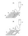
定量ポンプノズル方式は、図5(A)に示すように、タンク兼定量ポンプ10からノズル12へコーティング剤を定量供給すると共に、ノズル12をX−Yロボットにより回路基板14の半田付け部16の配列ラインに沿って定速移動させ、コーティング剤18を線状に塗布する方式である。 In the metering pump nozzle system, as shown in FIG. 5A, the coating agent is quantitatively supplied from the tank and
カーテンコート方式は、図5(B)に示すように、コーティング剤18を帯状に吐出できるスリットダイ20を用いて、コーティング剤18を面状に塗布する方式である。それ以外は上記方式と同様である(特許文献1)。 As shown in FIG. 5B, the curtain coating method is a method in which the
しかし、従来の塗布方法には次のような問題がある。すなわち、定量ポンプノズル方式は、線状塗布のため、個々の半田付け部への塗布精度が正確で、塗布量も比較的安定しているが、塗布速度が遅いという問題がある。一方、カーテンコート方式は、面状塗布のため、塗布速度は速いが、コーティング剤の飛び散り等のため塗布精度を向上させることが難しく、個々の半田付け部への塗布量が安定しないという問題がある。 However, the conventional coating method has the following problems. That is, since the metering pump nozzle system is linearly applied, the accuracy of application to each soldering part is accurate and the application amount is relatively stable, but there is a problem that the application speed is slow. On the other hand, the curtain coating method has a problem that the coating speed is fast because of the surface coating, but it is difficult to improve the coating accuracy due to scattering of the coating agent, and the amount of coating on the individual soldering parts is not stable. is there.
本発明の目的は、上記のような従来技術の問題点に鑑み、塗布速度が速く、塗布精度が正確で、個々の半田付け部への塗布量が安定な、回路基板半田付け部へのコーティング剤塗布方法と、それに用いる塗布装置を提供することにある。 In view of the above-mentioned problems of the prior art, the object of the present invention is to coat onto a circuit board soldering part with a high coating speed, an accurate coating accuracy, and a stable coating amount on each soldering part. An object of the present invention is to provide an agent coating method and a coating apparatus used therefor.
本発明に係る回路基板半田付け部へのコーティング剤塗布方法は、回路基板の多数の半田付け部と1対1で対応するように多数のノズルを設け、各ノズルから個々の半田付け部に適する塗布量となるように計量されたコーティング剤を同時に吐出して、多数の半田付け部に同時にコーティング剤を塗布することを特徴とするものである。 The method for applying a coating agent to a circuit board soldering portion according to the present invention is provided with a number of nozzles so as to correspond to the number of soldering portions of the circuit board on a one-to-one basis, and is suitable for each soldering portion from each nozzle. The coating agent measured so that it may become the application amount is simultaneously discharged, and the coating agent is simultaneously applied to a large number of soldering portions.
また、上記塗布方法に用いる本発明に係るコーティング剤塗布装置は、
回路基板の半田付け部に塗布するコーティング剤を貯留するタンクと、
このタンクの底板に回路基板の多数の半田付け部と1対1で対応するように設けられた多数のノズルと、
前記タンク内の底板上に設置され、前記多数のノズルと1対1で対応する多数の導通孔を有するシャッターと、
このシャッター上に設置され、前記多数のノズルと1対1で対応する多数のシリンダーを有するシリンダープレートと、
このシリンダープレートの多数のシリンダーに下端部が挿入され、上端部をピストンホルダーによって一括して上下動可能に保持された多数のピストンとを備え、
前記シリンダープレートはタンク内で移動できないように設置され、前記シャッターは各導通孔が対応するシリンダーとノズルを導通する位置と導通しない位置を往復移動できるように設置されていることを特徴とするものである。Moreover, the coating agent coating apparatus according to the present invention used for the coating method is as follows.
A tank for storing a coating agent to be applied to the soldering portion of the circuit board;
A number of nozzles provided on the bottom plate of the tank in a one-to-one correspondence with a number of soldering portions of the circuit board;
A shutter that is installed on a bottom plate in the tank and has a large number of conduction holes that correspond one-to-one with the large number of nozzles;
A cylinder plate having a number of cylinders installed on the shutter and corresponding one-to-one with the number of nozzles;
The lower end is inserted into many cylinders of this cylinder plate, and the upper end is provided with a plurality of pistons held together by a piston holder so as to be movable up and down.
The cylinder plate is installed so as not to move in the tank, and the shutter is installed so that each conduction hole can reciprocate between a position where the corresponding cylinder and nozzle are conducted and a position where the shutter is not conducted. It is.
また、本発明に係る上記塗布装置は、前記シャッターの、各導通孔からシャッターの往復移動距離だけ離れた位置に、各シリンダーへコーティング剤を供給するコモンレールが形成されており、このコモンレールには、シリンダープレートのシリンダー形成領域以外の領域に形成された開口を通してタンク内のコーティング剤が供給されるようになっていることが好ましい。 Further, in the coating apparatus according to the present invention, a common rail for supplying a coating agent to each cylinder is formed at a position separated from each conduction hole by a reciprocating distance of the shutter of the shutter. It is preferable that the coating agent in the tank is supplied through an opening formed in a region other than the cylinder forming region of the cylinder plate.
本発明によれば、回路基板の多数の半田付け部にコーティング剤を同時に塗布することができるので、コーティング剤塗布に要する時間を大幅に短縮することができる。また、ノズルと回路基板の相対位置を動かさないで塗布を行うので、塗布精度が正確になるだけでなく、コーティング剤中へのエア噛み込み、コーティング剤が塗布されない不濡れ、あるいは塗りズレなどの不良が発生するおそれがなくなる。さらに、個々の半田付け部にシリンダーで計量されたコーティング剤を塗布するので、個々の半田付け部への塗布量が一定となり、バラツキのない安定した塗布状態を得ることができる。 According to the present invention, since the coating agent can be simultaneously applied to a large number of soldered portions of the circuit board, the time required for applying the coating agent can be greatly shortened. In addition, since the application is performed without moving the relative position of the nozzle and the circuit board, not only the application accuracy becomes accurate, but also the air bites into the coating agent, the non-wetting that the coating agent is not applied, or the coating misalignment, etc. There is no risk of defects. Furthermore, since the coating agent measured by the cylinder is applied to each soldering portion, the amount applied to each soldering portion is constant, and a stable application state without variation can be obtained.
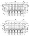
図1は本発明に係る回路基板半田付け部へのコーティング剤塗布方法に用いる塗布装置の一実施形態を示す。この塗布装置は、コーティング剤を貯留するタンク22を備えている。タンク22には、入口配管24Aからコーティング剤が流入し、余分なコーティング剤は出口配管24Bから流出して、常に新鮮なコーティング剤が貯留されるようになっている。タンク22には密閉カバー26が被せられ、コーティング剤の劣化を防止するようになっている。 FIG. 1 shows an embodiment of a coating apparatus used for a coating agent coating method for a circuit board soldering portion according to the present invention. This coating device includes a
タンク22の底板には、多数のノズル28が設けられている。これらのノズル28は、回路基板14の多数の半田付け部16と1対1で対応している。なお30は回路基板14に半田付けされた部品のリード等である。 A large number of
タンク22内の底板上にはシャッター32が設置され、シャッター32上にはシリンダープレート34が設置されている。シリンダープレート34には、前記多数のノズル28と1対1で対応するように多数のシリンダー36が形成されている。シリンダー36はシリンダープレート34を上下方向に貫通する孔で構成されている。またシャッター32には、各シリンダー36とノズル28を導通させるための多数の導通孔38が形成されている。シャッター32はタンク22の底板とシリンダープレート34との間で一方向に(紙面左右方向に)往復移動可能であるが、シリンダープレート34はタンク22内で移動できないように(シリンダー36とノズル28の位置がずれないように)設置されている。 A
さらに、シャッター32には、各導通孔38からシャッター32の往復移動ストローク(シリンダー36の配列ピッチの半分の距離)だけ離れた位置に、上向きに開口するコモンレール40が形成されている。このコモンレール40は、シリンダープレート34のシリンダー形成領域以外の領域に形成された開口(図示省略)を通してタンク22内のコーティング剤溜まりと連通している。これにより、タンク22内のコーティング剤は、シリンダープレート34の開口を通してコモンレール40に供給され、コモンレール40からシリンダー36に供給されるようになる(詳細は後述)。 Further, a
シリンダープレート34の各シリンダー36にはそれぞれ、ピストン42の下端部が挿入されている。各ピストン42は密閉カバー26を貫通しており、各ピストン42の上端部は密閉カバー26の外でピストンホルダー44によって一括して保持されている。つまり、全てのピストン42はピストンホルダー44を上下させることにより、一括して上下動するようになっている。 A lower end portion of a
次に、以上のように構成された塗布装置により、回路基板の半田付け部にコーティング剤を塗布する方法を図2及び図3を参照して説明する。まず図2(A)に示すように、タンク22内には入口配管24Aからコーティング剤18が供給され、余分なコーティング剤18は出口配管24Bから排出されて、タンク22内のコーティング剤18の量は一定に保たれている。 Next, a method for applying the coating agent to the soldering portion of the circuit board using the coating apparatus configured as described above will be described with reference to FIGS. First, as shown in FIG. 2A, the
図2(A)の初期状態では、ピストン42が下降位置にあり、シリンダー36内にはコーティング剤は入っていない。またシャッター32は、コモンレール40がシリンダー36と一致する位置(シリンダー36とノズル28の導通を遮断する位置)にある。コモンレール40には、タンク22内のコーティング剤18が、シリンダープレート34の図示しない開口を通して供給されている。タンク22の下には、各半田付け部16が対応するノズル28の真下に位置するように、回路基板14が位置決めされる。 In the initial state of FIG. 2A, the
この状態から、図2(B)に示すように全ピストン42を所定の上昇位置まで上昇させる。これによりコモンレール40内のコーティング剤18がシリンダー36内に吸入される(供給される)。シリンダー36の容積は、ピストン42が所定の上昇位置まで上昇したときに、シリンダー36内に吸入されるコーティング剤の量が1回分の塗布量となるように設定されている。 From this state, as shown in FIG. 2 (B), all the
次に、シャッター32を紙面で左方へ所定の距離だけ移動させる。すると図3(A)に示すように、シリンダー36とノズル28が、シャッター32の導通孔38を介して導通した状態となる。 Next, the
この状態で全ピストン42を下降させれば、図3(B)に示すように、各シリンダー36で計量されたコーティング剤18がノズル28から同時に吐出され、各半田付け部16に同時に塗布される。 If all the
従来の塗布方法は、図4(B)に示すように、回路基板14に対してノズル12(又はスリットダイ20)を移動させながらコーティング剤18を塗布する方式であるため、半田付け部16(半田フィレット)のノズル進行方向下り斜面にコーティング剤が塗布されない不濡れfが発生したり、塗布されたコーティング剤18がエアを噛み込むエア噛み込みeが発生したりしやすいという問題があった。これに対し本発明の塗布方法は、図4(A)に示すように、ノズル28を移動させずに半田フィレットの頂部からコーティング剤18を塗布する方式であるため、コーティング剤18が濡れ広がりやすく、かつシリンダーにより計量された規定量のコーティング剤を塗布する方式であるため、多数の半田付け部16に、位置、量ともに、均一で安定した塗布を行うことができる。 As shown in FIG. 4B, the conventional coating method is a method in which the
なお、上記の塗布装置では、ピストン42を上昇させたり、下降させたりするときに、シリンダープレート34が浮き上がることのないように(シャッター32から離れないように)、シリンダープレート34に図示しないスプリング等により上から押圧力を加えておくことが好ましい。 In the above application device, when the
14:回路基板
16:半田付け部
18:コーティング剤
22:タンク
24A、24B:配管
26:密閉カバー
28:ノズル
32:シャッター
34:シリンダープレート
36:シリンダー
38:導通孔
40:コモンレール
42:ピストン
44:ピストンホルダー14: Circuit board 16: Soldering part 18: Coating agent 22:
Claims (3)
Translated fromJapaneseこのタンクの底板に回路基板の複数の半田付け部と1対1で対応するように設けられた複数のノズルと、
前記タンク内の底板上に設置され、前記複数のノズルと1対1で対応する複数の導通孔を有するシャッターと、
このシャッター上に設置され、前記複数のノズルと1対1で対応する複数のシリンダーを有するシリンダープレートと、
このシリンダープレートの複数のシリンダーに下端部が挿入され、上端部をピストンホルダーによって一括して上下動可能に保持された複数のピストンとを備え、
前記シリンダープレートはタンク内で移動できないように設置され、前記シャッターは各導通孔が対応するシリンダーとノズルを導通する位置と導通しない位置を往復移動できるように設置されていることを特徴とする回路基板半田付け部へのコーティング剤塗布装置。A tank for storing a coating agent to be applied to the soldering portion of the circuit board;
A plurality of nozzles provided in a one-to-one correspondence with a plurality of soldering portions of the circuit board on the bottom plate of the tank;
A shutter installed on a bottom plate in the tank and having a plurality of conduction holes that correspond one-to-one with the plurality of nozzles;
A cylinder plate installed on the shutter and having a plurality of cylinders corresponding one-to-one with the plurality of nozzles;
The lower end portion is inserted into a plurality of cylinders of the cylinder plate, and the upper end portion is provided with a plurality of pistons held together by a piston holder so as to be movable up and down.
The cylinder plate is installed so as not to move in the tank, and the shutter is installed so that each conduction hole can reciprocate between a position where the corresponding cylinder and the nozzle are conducted and a position where the shutter is not conducted. Coating agent application device for board soldering part.
Priority Applications (1)
| Application Number | Priority Date | Filing Date | Title |
|---|---|---|---|
| JP2006041330AJP4558660B2 (en) | 2006-02-17 | 2006-02-17 | Coating agent application device for soldering part of circuit board |
Applications Claiming Priority (1)
| Application Number | Priority Date | Filing Date | Title |
|---|---|---|---|
| JP2006041330AJP4558660B2 (en) | 2006-02-17 | 2006-02-17 | Coating agent application device for soldering part of circuit board |
Publications (2)
| Publication Number | Publication Date |
|---|---|
| JP2007220992Atrue JP2007220992A (en) | 2007-08-30 |
| JP4558660B2 JP4558660B2 (en) | 2010-10-06 |
Family
ID=38497915
Family Applications (1)
| Application Number | Title | Priority Date | Filing Date |
|---|---|---|---|
| JP2006041330AActiveJP4558660B2 (en) | 2006-02-17 | 2006-02-17 | Coating agent application device for soldering part of circuit board |
Country Status (1)
| Country | Link |
|---|---|
| JP (1) | JP4558660B2 (en) |
Cited By (6)
| Publication number | Priority date | Publication date | Assignee | Title |
|---|---|---|---|---|
| WO2009104421A1 (en)* | 2008-02-21 | 2009-08-27 | 武蔵エンジニアリング株式会社 | Device and method for discharging liquid material |
| KR101345785B1 (en) | 2012-05-24 | 2013-12-27 | 필코씨앤디(주) | Flux or solder transferring device for chip mounting and mounting method of chip on the substrate |
| CN107716218A (en)* | 2017-11-17 | 2018-02-23 | 江门市蓬江区精汇电子科技有限公司 | A kind of equipment for the processing of LED charactrons encapsulating |
| CN107716219A (en)* | 2017-11-17 | 2018-02-23 | 江门市蓬江区精汇电子科技有限公司 | A kind of LED charactrons adhesive injection device with heater |
| CN107755189A (en)* | 2017-11-17 | 2018-03-06 | 江门市蓬江区精汇电子科技有限公司 | A kind of LED charactrons adhesive injection device |
| JP2021005932A (en)* | 2019-06-26 | 2021-01-14 | 三洋テクノソリューションズ鳥取株式会社 | Power supply board and manufacturing method for power supply board |
Citations (2)
| Publication number | Priority date | Publication date | Assignee | Title |
|---|---|---|---|---|
| JPH0367474U (en)* | 1989-11-06 | 1991-07-01 | ||
| JP2002329951A (en)* | 2001-05-02 | 2002-11-15 | Naka Liquid Control:Kk | Mounting substrate coating equipment and coating method |
- 2006
- 2006-02-17JPJP2006041330Apatent/JP4558660B2/enactiveActive
Patent Citations (2)
| Publication number | Priority date | Publication date | Assignee | Title |
|---|---|---|---|---|
| JPH0367474U (en)* | 1989-11-06 | 1991-07-01 | ||
| JP2002329951A (en)* | 2001-05-02 | 2002-11-15 | Naka Liquid Control:Kk | Mounting substrate coating equipment and coating method |
Cited By (9)
| Publication number | Priority date | Publication date | Assignee | Title |
|---|---|---|---|---|
| WO2009104421A1 (en)* | 2008-02-21 | 2009-08-27 | 武蔵エンジニアリング株式会社 | Device and method for discharging liquid material |
| CN102006943B (en)* | 2008-02-21 | 2013-07-24 | 武藏工业株式会社 | Discharging device for liquid material and coating device thereof |
| JP5340181B2 (en)* | 2008-02-21 | 2013-11-13 | 武蔵エンジニアリング株式会社 | Liquid material discharge apparatus and method |
| TWI457181B (en)* | 2008-02-21 | 2014-10-21 | Musashi Engineering Inc | A discharge device for a liquid material, a coating apparatus and a coating method therefor |
| KR101345785B1 (en) | 2012-05-24 | 2013-12-27 | 필코씨앤디(주) | Flux or solder transferring device for chip mounting and mounting method of chip on the substrate |
| CN107716218A (en)* | 2017-11-17 | 2018-02-23 | 江门市蓬江区精汇电子科技有限公司 | A kind of equipment for the processing of LED charactrons encapsulating |
| CN107716219A (en)* | 2017-11-17 | 2018-02-23 | 江门市蓬江区精汇电子科技有限公司 | A kind of LED charactrons adhesive injection device with heater |
| CN107755189A (en)* | 2017-11-17 | 2018-03-06 | 江门市蓬江区精汇电子科技有限公司 | A kind of LED charactrons adhesive injection device |
| JP2021005932A (en)* | 2019-06-26 | 2021-01-14 | 三洋テクノソリューションズ鳥取株式会社 | Power supply board and manufacturing method for power supply board |
Also Published As
| Publication number | Publication date |
|---|---|
| JP4558660B2 (en) | 2010-10-06 |
Similar Documents
| Publication | Publication Date | Title |
|---|---|---|
| JP4558660B2 (en) | Coating agent application device for soldering part of circuit board | |
| US7894919B2 (en) | Fully automated paste dispense system for dispensing small dots and lines | |
| KR101086376B1 (en) | Solder ball printing machine | |
| CN101772277B (en) | Apparatus for and method of coating flux with a movable nozzle | |
| CN110154505B (en) | Silk screen printer and silk screen printing process | |
| US10028392B2 (en) | Stencil set and system for printing solder paste for printed circuit boards | |
| US6591745B2 (en) | Screen printing apparatus and screen printing method | |
| US6553905B2 (en) | Screen printing method | |
| JPH10284830A (en) | Multi-dispenser type soldering device and method for soldering | |
| JP2020516500A (en) | Automatic solder paste adding device for solder paste printer | |
| US6711999B2 (en) | Screen printing apparatus | |
| JP3685053B2 (en) | Screen printing device | |
| US5590455A (en) | Apparatus for manufacturing a printed circuit board | |
| CN108738246A (en) | Device for removing residual tin cream automatically | |
| CN108738245A (en) | Automatic tin cream adding device for stencil printer | |
| KR101013984B1 (en) | Replaceable Nozzles of Solder Paste Printing Machines | |
| KR100645541B1 (en) | Solder Paste Printing Apparatus and Method | |
| JP7199507B2 (en) | Deposition equipment and mounter | |
| KR101366672B1 (en) | Chip die bonding method and chip die bonding apparatus | |
| CN213000908U (en) | Glue dispensing device | |
| CN214481560U (en) | Tin dropping machine capable of enabling tin dropping to be uniformly coated | |
| JP4387026B2 (en) | Screen printing method | |
| JP2870595B2 (en) | Cream solder application equipment | |
| JP5058008B2 (en) | Screen printing machine | |
| JPH11320822A (en) | Solder printing apparatus and solder printing method |
Legal Events
| Date | Code | Title | Description |
|---|---|---|---|
| A621 | Written request for application examination | Free format text:JAPANESE INTERMEDIATE CODE: A621 Effective date:20070601 | |
| A131 | Notification of reasons for refusal | Free format text:JAPANESE INTERMEDIATE CODE: A131 Effective date:20100412 | |
| A521 | Written amendment | Free format text:JAPANESE INTERMEDIATE CODE: A523 Effective date:20100611 | |
| TRDD | Decision of grant or rejection written | ||
| A01 | Written decision to grant a patent or to grant a registration (utility model) | Free format text:JAPANESE INTERMEDIATE CODE: A01 Effective date:20100708 | |
| A01 | Written decision to grant a patent or to grant a registration (utility model) | Free format text:JAPANESE INTERMEDIATE CODE: A01 | |
| A61 | First payment of annual fees (during grant procedure) | Free format text:JAPANESE INTERMEDIATE CODE: A61 Effective date:20100721 | |
| R151 | Written notification of patent or utility model registration | Ref document number:4558660 Country of ref document:JP Free format text:JAPANESE INTERMEDIATE CODE: R151 | |
| FPAY | Renewal fee payment (event date is renewal date of database) | Free format text:PAYMENT UNTIL: 20130730 Year of fee payment:3 | |
| S531 | Written request for registration of change of domicile | Free format text:JAPANESE INTERMEDIATE CODE: R313531 | |
| R350 | Written notification of registration of transfer | Free format text:JAPANESE INTERMEDIATE CODE: R350 |