JP2007219852A - Memory system - Google Patents
Memory systemDownload PDFInfo
- Publication number
- JP2007219852A JP2007219852AJP2006039853AJP2006039853AJP2007219852AJP 2007219852 AJP2007219852 AJP 2007219852AJP 2006039853 AJP2006039853 AJP 2006039853AJP 2006039853 AJP2006039853 AJP 2006039853AJP 2007219852 AJP2007219852 AJP 2007219852A
- Authority
- JP
- Japan
- Prior art keywords
- optical
- signal
- memory
- electrical
- converter
- Prior art date
- Legal status (The legal status is an assumption and is not a legal conclusion. Google has not performed a legal analysis and makes no representation as to the accuracy of the status listed.)
- Pending
Links
Images


Classifications
- G—PHYSICS
- G06—COMPUTING OR CALCULATING; COUNTING
- G06F—ELECTRIC DIGITAL DATA PROCESSING
- G06F13/00—Interconnection of, or transfer of information or other signals between, memories, input/output devices or central processing units
- G06F13/38—Information transfer, e.g. on bus
- G06F13/42—Bus transfer protocol, e.g. handshake; Synchronisation
- G06F13/4204—Bus transfer protocol, e.g. handshake; Synchronisation on a parallel bus
- G06F13/4234—Bus transfer protocol, e.g. handshake; Synchronisation on a parallel bus being a memory bus
- G06F13/4243—Bus transfer protocol, e.g. handshake; Synchronisation on a parallel bus being a memory bus with synchronous protocol
- G—PHYSICS
- G11—INFORMATION STORAGE
- G11C—STATIC STORES
- G11C5/00—Details of stores covered by group G11C11/00
- G11C5/06—Arrangements for interconnecting storage elements electrically, e.g. by wiring
- G11C5/066—Means for reducing external access-lines for a semiconductor memory clip, e.g. by multiplexing at least address and data signals
- G—PHYSICS
- G11—INFORMATION STORAGE
- G11C—STATIC STORES
- G11C7/00—Arrangements for writing information into, or reading information out from, a digital store
- G11C7/10—Input/output [I/O] data interface arrangements, e.g. I/O data control circuits, I/O data buffers
- G11C7/1006—Data managing, e.g. manipulating data before writing or reading out, data bus switches or control circuits therefor
Landscapes
- Engineering & Computer Science (AREA)
- Theoretical Computer Science (AREA)
- Physics & Mathematics (AREA)
- General Engineering & Computer Science (AREA)
- General Physics & Mathematics (AREA)
- Optical Communication System (AREA)
- Memory System (AREA)
Abstract
Translated fromJapaneseDescription
Translated fromJapanese本発明は、メモリデバイスと、メモリデバイスをアクセスするためのメモリコントローラとを有するメモリシステムに関する。 The present invention relates to a memory system having a memory device and a memory controller for accessing the memory device.
CPU等のマイクロコントローラの性能は、年々向上している。これに伴い、マイクロコントローラによりアクセスされるメモリデバイスおよびメモリコントローラも性能を向上する必要がある。具体的には、マイクロコントローラとメモリデバイス間でのデータ信号等の伝送レート(バンド幅)を向上する必要がある。伝送レートを向上するために、ある種のメモリデバイスは、データ信号のビット数を増やしている。別のメモリデバイスは、高い周波数のクロックを用いて直列のデータ信号を伝送するインタフェース回路を搭載している。さらに、高い周波数のクロックを用いて複数ビットからなるデータ信号を伝送するインタフェース回路が検討されている。 The performance of microcontrollers such as CPUs is improving year by year. Accordingly, it is necessary to improve the performance of the memory device and the memory controller accessed by the microcontroller. Specifically, it is necessary to improve the transmission rate (bandwidth) of data signals and the like between the microcontroller and the memory device. In order to improve the transmission rate, some memory devices increase the number of bits of the data signal. Another memory device includes an interface circuit that transmits a serial data signal using a high-frequency clock. Further, an interface circuit that transmits a data signal composed of a plurality of bits using a high-frequency clock has been studied.
また、従来のメモリデバイスのインタフェース回路は、電気信号を用いている。電気信号の伝送レートの上限は、10Gbps程度と言われており、これを超える伝送レートが必要な場合、光信号等を用いた新たなインタフェース回路を検討する必要がある。 The interface circuit of the conventional memory device uses an electrical signal. The upper limit of the transmission rate of electrical signals is said to be about 10 Gbps. When a transmission rate exceeding this is required, it is necessary to consider a new interface circuit using an optical signal or the like.
例えば、マイクロコントローラとメモリコントローラとの間に、光インタフェースを適用する技術が提案されている(例えば、特許文献1参照)。
しかしながら、特許文献1では、メモリコントローラとメモリデバイスとの間のインタフェースの詳細は、記載されていない。すなわち、メモリコントローラとメモリデバイスとの間で伝送される信号の伝送レート向上する手法は、開示されていない。 However,
本発明の目的は、メモリコントローラとメモリデバイスとの間で伝送される信号の伝送レートを、最小限のコストで向上することにある。 An object of the present invention is to improve the transmission rate of signals transmitted between a memory controller and a memory device at a minimum cost.
本発明の一形態では、メモリコントローラは、複数ビットからなるアクセス信号を光信号として多重化し、多重化した光信号を複数のメモリデバイスをアクセスするために出力する。この際、メモリコントローラは、メモリデバイス毎に波長が異なる光信号を生成し、生成した光信号を多重化する。多重化により信号の伝送レートは向上する。メモリインタフェースユニットは、メモリコントローラからの多重化された光信号を元の光信号に分離し、分離した光信号を電気信号に変換する。この際、メモリインタフェースユニットは、変換した電気信号のメモリデバイスへの出力先を、分離した光信号の波長に応じて決める。これにより、メモリコントローラは、アクセスするメモリデバイスを識別する信号を、メモリインタフェースユニットに伝送する必要がない。メモリインタフェースユニットは、アクセスするメモリデバイスを識別するためのデコード回路を形成する必要がない。したがって、メモリコントローラとメモリデバイスとの間で伝送される信号の伝送レートを、最小限のコストで向上できる。 In one embodiment of the present invention, a memory controller multiplexes an access signal composed of a plurality of bits as an optical signal, and outputs the multiplexed optical signal for accessing a plurality of memory devices. At this time, the memory controller generates optical signals having different wavelengths for each memory device, and multiplexes the generated optical signals. Multiplexing improves the signal transmission rate. The memory interface unit separates the multiplexed optical signal from the memory controller into the original optical signal, and converts the separated optical signal into an electrical signal. At this time, the memory interface unit determines the output destination of the converted electrical signal to the memory device according to the wavelength of the separated optical signal. This eliminates the need for the memory controller to transmit a signal identifying the memory device to be accessed to the memory interface unit. The memory interface unit does not need to form a decoding circuit for identifying the memory device to be accessed. Therefore, the transmission rate of signals transmitted between the memory controller and the memory device can be improved at a minimum cost.
本発明の一形態における好ましい例では、メモリコントローラにおいて、第1電気/光変換器は、アクセス信号(電気信号)を光信号に変換する。第1光合波器は、第1電気/
光変換器により変換された光信号を多重化する。メモリインタフェースユニットにおいて、第1光分波器は、第1光合波器により多重化された光信号を、元の光信号に分離する。第1光/電気変換器は、分離された光信号を電気信号に変換する。これにより、メモリコントローラからメモリインタフェースユニットに伝送される信号の伝送レートを向上できる。In a preferred example of one aspect of the present invention, in the memory controller, the first electrical / optical converter converts an access signal (electrical signal) into an optical signal. The first optical multiplexer is connected to the first electric /
The optical signal converted by the optical converter is multiplexed. In the memory interface unit, the first optical demultiplexer separates the optical signal multiplexed by the first optical multiplexer into the original optical signal. The first optical / electrical converter converts the separated optical signal into an electrical signal. Thereby, the transmission rate of the signal transmitted from the memory controller to the memory interface unit can be improved.
本発明の一形態における好ましい例では、メモリインタフェースユニットにおいて、第2電気/光変換器は、メモリデバイスから出力される電気信号を波長が互いに異なる光信号に変換する。第2光合波器は、第2電気/光変換器により変換された光信号を多重化する。メモリコントローラにおいて、第2光分波器は、第2光合波器により多重化された光信号を、元の光信号に分離する。第2光/電気変換器は、分離された光信号を電気信号に変換する。これにより、メモリインタフェースユニットからメモリコントローラに伝送される信号の伝送レートを向上できる。 In a preferred example of one aspect of the present invention, in the memory interface unit, the second electrical / optical converter converts electrical signals output from the memory device into optical signals having different wavelengths. The second optical multiplexer multiplexes the optical signal converted by the second electric / optical converter. In the memory controller, the second optical demultiplexer separates the optical signal multiplexed by the second optical multiplexer into the original optical signal. The second optical / electrical converter converts the separated optical signal into an electrical signal. Thereby, the transmission rate of the signal transmitted from the memory interface unit to the memory controller can be improved.
本発明の一形態における好ましい例では、メモリコントローラにおいて、第1シリアライザは、並列のアクセス信号を直列信号にそれぞれ変換し、変換した直列信号を第1電気/光変換器に出力する。メモリインタフェースユニットにおいて、第1デシリアライザは、第1光/電気変換器により変換された直列信号を並列信号に変換する。これにより、第1電気/光変換器および第1光/電気変換器の数を減らすことができ、第1光合波器および第1光分波器の回路規模を削減できる。すなわち、メモリコントローラからメモリインタフェースユニットに信号を伝送するためのコストを削減できる。 In a preferred example of one aspect of the present invention, in the memory controller, the first serializer converts each parallel access signal into a serial signal, and outputs the converted serial signal to the first electrical / optical converter. In the memory interface unit, the first deserializer converts the serial signal converted by the first optical / electrical converter into a parallel signal. Thereby, the number of 1st electric / optical converters and 1st optical / electrical converters can be reduced, and the circuit scale of a 1st optical multiplexer and a 1st optical demultiplexer can be reduced. That is, the cost for transmitting signals from the memory controller to the memory interface unit can be reduced.
本発明の一形態における好ましい例では、メモリインタフェースユニットにおいて、第2シリアライザは、メモリデバイスから出力される並列の電気信号を直列信号にそれぞれ変換し、第2電気/光変換器に出力する。メモリコントローラにおいて、第2デシリアライザは、第2光/電気変換器により変換された直列の電気信号を並列信号に変換する。これにより、第2電気/光変換器および第2光/電気変換器の数を減らすことができ、第2光合波器および第2光分波器の回路規模を削減できる。すなわち、メモリインタフェースユニットからメモリコントローラに信号を伝送するためのコストを削減できる。 In a preferred example of one aspect of the present invention, in the memory interface unit, the second serializer converts parallel electric signals output from the memory device into serial signals, and outputs the serial signals to the second electric / optical converter. In the memory controller, the second deserializer converts the serial electrical signal converted by the second optical / electrical converter into a parallel signal. As a result, the number of second electrical / optical converters and second optical / electrical converters can be reduced, and the circuit scale of the second optical multiplexer and second optical demultiplexer can be reduced. That is, the cost for transmitting signals from the memory interface unit to the memory controller can be reduced.
本発明の一形態における好ましい例では、メモリインタフェースユニットにおいて、第1タイミング調整器は、第1光/電気変換器により変換された電気信号のタイミングを調整する。例えば、第1タイミング調整器は、同種の電気信号のスキューを取り除くデスキュー回路と、デスキュー回路によりスキューが取り除かれた電気信号のサイクルを互いに合わせるサイクル調整回路とを有している。これにより、光伝送により信号の位相がずれた場合にも伝送レートを下げることなく正しい信号を送受信できる。特に、メモリコントローラとメモリデバイスとの距離が大きい等、信号の位相がずれやすい環境においても、伝送レートを下げることなく正しい信号を送受信できる。 In a preferred example of one aspect of the present invention, in the memory interface unit, the first timing adjuster adjusts the timing of the electrical signal converted by the first optical / electrical converter. For example, the first timing adjuster includes a deskew circuit that removes the skew of the same type of electric signal and a cycle adjustment circuit that matches the cycles of the electric signal from which the skew has been removed by the deskew circuit. Thereby, even when the signal phase is shifted due to optical transmission, a correct signal can be transmitted and received without lowering the transmission rate. In particular, even in an environment where the phase of the signal is likely to shift, such as when the distance between the memory controller and the memory device is large, a correct signal can be transmitted and received without lowering the transmission rate.
本発明の一形態における好ましい例では、メモリコントローラにおいて、第1波長変換器は、アクセス信号(光信号)の波長を、アクセスするメモリデバイス毎に異なる波長に変換する。第1光合波器は、第1波長変換器により変換された光信号を多重化する。メモリインタフェースユニットにおいて、第1光分波器は、第1光合波器により多重化された光信号を、元の光信号に分離する。第1光/電気変換器は、分離された光信号を電気信号に変換する。これにより、メモリコントローラが光信号を扱う場合にも、光ケーブルにより複数のメモリデバイスをアクセスできる。この結果、最小限のコストで信号の伝送レートを向上できる。 In a preferred example of one aspect of the present invention, in the memory controller, the first wavelength converter converts the wavelength of the access signal (optical signal) into a different wavelength for each memory device to be accessed. The first optical multiplexer multiplexes the optical signal converted by the first wavelength converter. In the memory interface unit, the first optical demultiplexer separates the optical signal multiplexed by the first optical multiplexer into the original optical signal. The first optical / electrical converter converts the separated optical signal into an electrical signal. Thereby, even when the memory controller handles an optical signal, a plurality of memory devices can be accessed by the optical cable. As a result, the signal transmission rate can be improved at a minimum cost.
本発明の一形態における好ましい例では、コマンド体系が互いに異なる異種のメモリデバイスに入出力される信号が多重化され伝送される。したがって、信号の伝送レートを向
上できる。In a preferred example of one embodiment of the present invention, signals input / output to / from different types of memory devices having different command systems are multiplexed and transmitted. Therefore, the signal transmission rate can be improved.
本発明の一形態における好ましい例では、メモリコントローラは、メモリデバイスの少なくとも1つに対して、読み出し動作用のアクセス信号と書き込み動作用のアクセス信号とを互いに独立して出力する。メモリデバイスの少なくとも1つは、読み出し動作用のアクセス信号と書き込み動作用のアクセス信号とを互いに独立して受信する。メモリデバイスの読み出し動作および書き込み動作を独立して実行できるため、信号の伝送レートをさらに向上できる。 In a preferred example of one aspect of the present invention, the memory controller outputs an access signal for read operation and an access signal for write operation independently of each other to at least one of the memory devices. At least one of the memory devices receives an access signal for a read operation and an access signal for a write operation independently of each other. Since the read operation and the write operation of the memory device can be performed independently, the signal transmission rate can be further improved.
本発明の一形態における好ましい例では、メモリデバイス少なくとも1つは、独立に動作可能な複数のメモリブロックを有している。メモリコントローラは、メモリブロックを有するメモリデバイスに対してメモリブロック毎に独立したアクセス信号を出力する。メモリブロックを有するメモリデバイスは、メモリブロック毎に独立したアクセス信号を受信する。メモリブロックを独立にアクセスできるため、信号の伝送レートをさらに向上できる。 In a preferred example of one aspect of the present invention, at least one memory device has a plurality of independently operable memory blocks. The memory controller outputs an independent access signal for each memory block to the memory device having the memory block. A memory device having a memory block receives an independent access signal for each memory block. Since the memory block can be accessed independently, the signal transmission rate can be further improved.
メモリコントローラとメモリデバイスとの間で伝送される信号の伝送レートを、最小限のコストで向上できる。 The transmission rate of signals transmitted between the memory controller and the memory device can be improved at a minimum cost.
以下、本発明の実施形態を図面を用いて説明する。図中、太線で示した信号線は、複数本で構成されている。また、太線が接続されているブロックの一部は、複数の回路で構成されている。また、信号が伝達される信号線には、信号名と同じ符号を使用する。 Hereinafter, embodiments of the present invention will be described with reference to the drawings. In the figure, the signal lines indicated by bold lines are composed of a plurality of lines. A part of the block to which the thick line is connected is composed of a plurality of circuits. Further, the same reference numerals as the signal names are used for signal lines through which signals are transmitted.
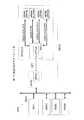
図1は、本発明の第1の実施形態を示している。この実施形態では、メモリシステムMSYSは、メモリコントローラMCNTおよびメモリモジュールMODULEにより構成されている。メモリモジュールMODULEは、1本の光ケーブルOPTによりメモリコントローラMCNTに接続されている。メモリコントローラMCNTは、CPU(マイクロプロセッサ)、DMACおよび周辺デバイスPERI1−2とともにシステムバスSBUSに接続されている。システムバスSBUSは電気的インタフェースを有している。 FIG. 1 shows a first embodiment of the present invention. In this embodiment, the memory system MSYS is composed of a memory controller MCNT and a memory module MODULE. The memory module MODULE is connected to the memory controller MCNT by one optical cable OPT. The memory controller MCNT is connected to the system bus SBUS together with a CPU (microprocessor), a DMAC, and a peripheral device PERI1-2. The system bus SBUS has an electrical interface.
メモリコントローラMCNTは、光変換ユニットOPTU1および図示しない光コネクタを、プリント基板等に搭載して形成されている。メモリモジュールMODULEは、メモリインタフェースユニットMIFUおよびメモリデバイスMEM(MEMA、MEMB、MEMC、MEMD)を、プリント基板等に搭載して形成されている。メモリインタフェースユニットMIFUは、光変換ユニットOPTU2および図示しない光コネクタを搭載して形成されている。メモリデバイスMEMA、MEMB、MEMC、MEMDは、高速SRAM、フラッシュメモリFLASH、DRAM、DRAMである。 The memory controller MCNT is formed by mounting an optical conversion unit OPTU1 and an optical connector (not shown) on a printed circuit board or the like. The memory module MODULE is formed by mounting a memory interface unit MIFU and a memory device MEM (MEMA, MEMB, MEMC, MEMD) on a printed circuit board or the like. The memory interface unit MIFU is formed by mounting an optical conversion unit OPTU2 and an optical connector (not shown). The memory devices MEMA, MEMB, MEMC, and MEMD are high-speed SRAM, flash memory FLASH, DRAM, and DRAM.
メモリデバイスMEMは、クロック同期式でもクロック非同期式でもよい。メモリモジュールMODULEにクロック同期式のメモリデバイスMEMを搭載する場合、クロック信号を供給する必要がある。この場合、クロック信号の周波数は、メモリデバイスMEM毎に異なっていてもよい。クロック信号は、光ケーブルOPTを介して供給してもよく、別のケーブル(電気ケーブルまたは光ケーブル)を介して供給してもよい。 The memory device MEM may be a clock synchronous type or a clock asynchronous type. When a clock synchronous memory device MEM is mounted on the memory module MODULE, it is necessary to supply a clock signal. In this case, the frequency of the clock signal may be different for each memory device MEM. The clock signal may be supplied via the optical cable OPT or may be supplied via another cable (electric cable or optical cable).
本発明では、メモリデバイスMEMは、メモリコントローラMCNTを介してCPUおよびDMACによりアクセスされる。メモリコントローラMCNTとメモリモジュールMODULEの間では、情報は、光信号を用いて伝送される。光伝送は、例えば、WDM(Wavelength Division Multiplex)方式を用いて行われる。本発明に適用可能なWDM方式
として、例えば、DWDM(Dense WDM)およびCWDM(Coarse WDM)等がある。これにより、4つのメモリデバイスMEMをアクセスするための多ビットからなるアクセス信号を、1本の光ケーブルOPTにより伝送できる。ここで、アクセス信号は、メモリデバイスMEMをアクセスするコマンド信号の他に、メモリデバイスMEMに書き込まれるデータ信号およびメモリデバイスMEMから読み出されるデータ信号を含んでいる。In the present invention, the memory device MEM is accessed by the CPU and DMAC via the memory controller MCNT. Information is transmitted between the memory controller MCNT and the memory module MODULE using an optical signal. The optical transmission is performed using, for example, a WDM (Wavelength Division Multiplex) method. Examples of WDM systems applicable to the present invention include DWDM (Dense WDM) and CWDM (Coarse WDM). Thereby, an access signal composed of multiple bits for accessing the four memory devices MEM can be transmitted by one optical cable OPT. Here, the access signal includes a data signal written to the memory device MEM and a data signal read from the memory device MEM, in addition to a command signal for accessing the memory device MEM.
メモリデバイスMEMA(SRAM)へのアクセス信号として、コマンド信号CMDA、アドレス信号ADAおよびデータ信号DTAがある。例えば、コマンド信号CMDAは、チップセレクト信号/CS、ライトイネーブル信号/WEおよびアウトプットイネーブル信号/OEにより構成される。メモリデバイスMEMB(FLASH)へのアクセス信号として、コマンド信号CMDBおよびデータ信号DTBがある。例えば、コマンド信号CMDBは、コマンドラッチイネーブルCLE、アドレスラッチイネーブルALE、チップイネーブル信号/CE等により構成される。 As an access signal to the memory device MEMA (SRAM), there are a command signal CMDA, an address signal ADA, and a data signal DTA. For example, the command signal CMDA includes a chip select signal / CS, a write enable signal / WE, and an output enable signal / OE. There are a command signal CMDB and a data signal DTB as access signals to the memory device MEMB (FLASH). For example, the command signal CMDB includes a command latch enable CLE, an address latch enable ALE, a chip enable signal / CE, and the like.
メモリデバイスMEMC(DRAM)へのアクセス信号として、コマンド信号CMDC、アドレス信号ADCおよびデータ信号DTCがある。同様に、メモリデバイスMEMD(DRAM)へのアクセス信号として、コマンド信号CMDD、アドレス信号ADD、データ信号DTDがある。例えば、コマンド信号CMDC、CMDDは、チップセレクト信号/CS、ロウアドレスストローブ信号/RAS、コラムアドレスストローブ信号/CAS等によりそれぞれ構成される。 As an access signal to the memory device MEMC (DRAM), there are a command signal CMDC, an address signal ADC, and a data signal DTC. Similarly, there are a command signal CMDD, an address signal ADD, and a data signal DTD as access signals to the memory device MEMD (DRAM). For example, the command signals CMDC and CMDD are constituted by a chip select signal / CS, a row address strobe signal / RAS, a column address strobe signal / CAS, etc., respectively.
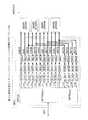
図2は、図1に示したメモリコントローラMCNTの詳細を示している。メモリコントローラMCNTは、論理回路LOGICおよび光変換ユニットOPTU1を有している。論理回路LOGICは、電気的なデジタル回路である。論理回路LOGICは、システムバスSBUSを介して供給されるアクセス信号(CMDA1−3、ADA0−2等)を光変換ユニットOPTU1に出力する。また、論理回路LOGICは、光変換ユニットOPTU1を介して受けるメモリデバイスMEM(MEMA、MEMB、MEMC、MEMD)からの読み出しデータRDT(RDTA、RDTB、RDTC、RDTD;図では、RDTD13−15のみを示す)をシステムバスSBUSに出力する。 FIG. 2 shows details of the memory controller MCNT shown in FIG. The memory controller MCNT has a logic circuit LOGIC and an optical conversion unit OPTU1. The logic circuit LOGIC is an electrical digital circuit. The logic circuit LOGIC outputs access signals (CMDA1-3, ADA0-2, etc.) supplied via the system bus SBUS to the optical conversion unit OPTU1. In addition, the logic circuit LOGIC shows read data RDT (RDTA, RDTB, RDTC, RDTD; RDTD13-15 only from the memory device MEM (MEMA, MEMB, MEMC, MEMD) received via the optical conversion unit OPTU1. ) To the system bus SBUS.
例えば、メモリデバイスMEMAをアクセスするためのコマンド信号CMDAは、3ビット(CMDA1−3)である。メモリデバイスMEMAをアクセスするアドレス信号ADAは、22ビット(ADA0−21)である。メモリデバイスMEMAに書き込まれるデータ信号DTAは、16ビットである。データ信号DTAは、書き込みデータ信号WDTA0−15および読み出しデータ信号RDTA0−15として論理回路LOGICに入出力される。他のメモリデバイスMEMB、MEMC、MEMDも同様に、複数ビットからなるコマンド信号およびデータ信号等が入出力される。 For example, the command signal CMDA for accessing the memory device MEMA is 3 bits (CMDA1-3). The address signal ADA for accessing the memory device MEMA is 22 bits (ADA0-21). The data signal DTA written to the memory device MEMA is 16 bits. The data signal DTA is input / output to / from the logic circuit LOGIC as a write data signal WDTA0-15 and a read data signal RDTA0-15. Similarly, other memory devices MEMB, MEMC, and MEMD also input / output command signals and data signals composed of a plurality of bits.
光変換ユニットOPTU1は、複数の第1電気/光変換器E/O1、複数の第2光/電気変換器O/E2、第1光合波器OPTMUL1および第2光分波器OPTDMUL2を有している。電気/光変換器E/O1は、論理回路LOGICから供給されるアクセス信号の各ビットに対応して配置されている。各電気/光変換器E/O1は、アクセス信号の各ビットを所定の波長λ(λ1−6等)の光信号に変換する。このように、電気/光変換器E/O1から出力される光信号の波長λは、アクセス(読み書き)するメモリデバイスMEM毎に異なっている。 The optical conversion unit OPTU1 includes a plurality of first electric / optical converters E / O1, a plurality of second optical / electrical converters O / E2, a first optical multiplexer OPTMUL1, and a second optical demultiplexer OPTDMUL2. Yes. The electrical / optical converter E / O1 is arranged corresponding to each bit of the access signal supplied from the logic circuit LOGIC. Each electric / optical converter E / O1 converts each bit of the access signal into an optical signal having a predetermined wavelength λ (λ1-6, etc.). As described above, the wavelength λ of the optical signal output from the electrical / optical converter E / O1 is different for each memory device MEM to be accessed (read / write).
光合波器OPTMULは、電気/光変換器E/O1からの光信号を多重化し、多重化した光信号を光ケーブルOPTに出力する。光分波器OPTDMULは、光ケーブルOPTを介して受信する多重化された光信号(読み出しデータ信号RDT)を分離し、分離した光信号を光/電気変換器O/E2に出力する。光/電気変換器O/E2は、光分波器OP
TDMULからの光信号を電気信号に変換する。The optical multiplexer OPTMUL multiplexes the optical signal from the electrical / optical converter E / O1, and outputs the multiplexed optical signal to the optical cable OPT. The optical demultiplexer OPTDMUL separates the multiplexed optical signal (read data signal RDT) received via the optical cable OPT, and outputs the separated optical signal to the optical / electrical converter O / E2. The optical / electrical converter O / E2 is an optical demultiplexer OP.
An optical signal from TDMUL is converted into an electric signal.
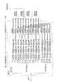
図3は、図1に示したメモリインタフェースユニットMIFUの詳細を示している。メモリインタフェースユニットMIFUは、第1光分波器OPTDMUL1、第2光合波器OPTMUL2、複数の第1光/電気変換器O/E1、および複数の第2電気/光変換器E/O2を有している。 FIG. 3 shows details of the memory interface unit MIFU shown in FIG. The memory interface unit MIFU includes a first optical demultiplexer OPTDMUL1, a second optical multiplexer OPTMUL2, a plurality of first optical / electrical converters O / E1, and a plurality of second electrical / optical converters E / O2. ing.
光分波器OPTDMUL1は、光ケーブルOPTを介して受信する多重化された光信号(アクセス信号)を分離し、分離した光信号を光/電気変換器O/E1に出力する。光/電気変換器O/E1は、光分波器OPTDMUL1により分離された光信号を電気信号(アクセス信号)に変換し、対応するメモリデバイスMEMに出力する。すなわち、光分波器OPTDMUL1は、光信号の波長λに応じて、受けた光信号のメモリデバイスMEMへの出力先を決める機能を有している。 The optical demultiplexer OPTDMUL1 separates the multiplexed optical signal (access signal) received via the optical cable OPT and outputs the separated optical signal to the optical / electrical converter O / E1. The optical / electrical converter O / E1 converts the optical signal separated by the optical demultiplexer OPTDMUL1 into an electrical signal (access signal) and outputs it to the corresponding memory device MEM. That is, the optical demultiplexer OPTDMUL1 has a function of determining the output destination of the received optical signal to the memory device MEM according to the wavelength λ of the optical signal.
電気/光変換器E/O2は、メモリデバイスMEMから読み出されたデータ信号RDTを波長が互いに異なる光信号に変換する。光合波器OPTMUL2は、電気/光変換器E/O2からの光信号を多重化し、多重化した光信号を光ケーブルOPTに出力する。 The electrical / optical converter E / O2 converts the data signal RDT read from the memory device MEM into optical signals having different wavelengths. The optical multiplexer OPTMUL2 multiplexes the optical signal from the electrical / optical converter E / O2, and outputs the multiplexed optical signal to the optical cable OPT.
メモリインタフェースユニットMIFUは、メモリコントローラMCNTから見ると論理的に透過している(トランスペアレント性)。すなわち、メモリコントローラMCNTによるメモリインタフェースユニットMIFUを介するアクセスは、各メモリデバイスMEMが直接アクセスされるのと等価である。 The memory interface unit MIFU is logically transparent when viewed from the memory controller MCNT (transparency). That is, the access through the memory interface unit MIFU by the memory controller MCNT is equivalent to the direct access of each memory device MEM.
以上、第1の実施形態では、メモリコントローラMCNTは、アクセスするメモリデバイスMEMを識別する信号を、メモリインタフェースユニットMIFUに伝送する必要がない。メモリインタフェースユニットMIFUは、アクセスするメモリデバイスMEMを識別するためのデコード回路等を形成する必要がない。したがって、メモリコントローラMCNTとメモリデバイスMEMとの間で伝送される信号の伝送レートを、最小限のコストで向上できる。 As described above, in the first embodiment, the memory controller MCNT does not need to transmit a signal for identifying the memory device MEM to be accessed to the memory interface unit MIFU. The memory interface unit MIFU does not need to form a decoding circuit or the like for identifying the memory device MEM to be accessed. Therefore, the transmission rate of signals transmitted between the memory controller MCNT and the memory device MEM can be improved at a minimum cost.
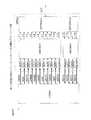
図4および図5は、本発明の第2の実施形態におけるメモリコントローラMCNTおよびメモリインタフェースユニットMIFUの詳細を示している。第1の実施形態で説明した要素と同一の要素については、同一の符号を付し、これ等については、詳細な説明を省略する。図4に示すように、メモリコントローラMCNTは、第1電気/光変換器E/O1の入力に直列に接続された第1エンコーダENC1および第1シリアライザSER1と、第2光/電気変換器O/E2の出力に直列に接続された第2デシリアライザDES2および第2デコーダDEC2とを有している。 4 and 5 show details of the memory controller MCNT and the memory interface unit MIFU in the second embodiment of the present invention. The same elements as those described in the first embodiment are denoted by the same reference numerals, and detailed description thereof will be omitted. As shown in FIG. 4, the memory controller MCNT includes a first encoder ENC1 and a first serializer SER1 connected in series to the input of the first electric / optical converter E / O1, and a second optical / electrical converter O / A second deserializer DES2 and a second decoder DEC2 connected in series to the output of E2.
図5に示すように、メモリインタフェースユニットMIFUは、第1光/電気変換器O/E1の出力に直列に接続された第1デシリアライザDES1および第1デコーダDEC1と、第2電気/光変換器E/O2の入力に直列に接続された第2エンコーダENC2および第2シリアライザSER2とを有している。すなわち、この実施形態では、電気信号は、光信号に変換される前にシリアライザSER1、SER2により並列直列変換される。光信号は電気信号に変換された後に、デシリアライザDES1−2により直列並列変換される。その他の構成は、第1の実施形態と同じである。 As shown in FIG. 5, the memory interface unit MIFU includes a first deserializer DES1 and a first decoder DEC1 connected in series to the output of the first optical / electrical converter O / E1, and a second electrical / optical converter E. The second encoder ENC2 and the second serializer SER2 connected in series to the input of / O2. In other words, in this embodiment, the electric signal is converted into a serial signal by the serializers SER1 and SER2 before being converted into an optical signal. The optical signal is converted into an electrical signal, and then converted in series and parallel by the deserializer DES1-2. Other configurations are the same as those of the first embodiment.
図4において、エンコーダENC1は、例えば、8B10Bエンコーダである。シリアライザSER1は、エンコーダENC1により符号化された並列のアクセス信号を直列信号に変換する。電気/光変換器E/O1は、直列に変換された信号を所定の波長λの光信号に変換する。 In FIG. 4, the encoder ENC1 is, for example, an 8B10B encoder. The serializer SER1 converts the parallel access signal encoded by the encoder ENC1 into a serial signal. The electrical / optical converter E / O1 converts the signal converted in series into an optical signal having a predetermined wavelength λ.
電気/光変換器O/E1および光分波器OPTDMUL2から出力される光信号の波長λ1−15は、アクセス(読み書き)するメモリデバイスMEM毎に互いに異なっている。具体的には、メモリデバイスMEMAのアクセスには、波長λ1、λ2、λ3、λ12が使用される。メモリデバイスMEMBのアクセスには、波長λ4、λ5、λ13が使用される。メモリデバイスMEMCのアクセスには、波長λ6、λ7、λ8、λ14が使用される。メモリデバイスMEMDのアクセスには、波長λ9、λ10、λ11、λ15が使用される。 The wavelengths λ1-15 of the optical signals output from the electrical / optical converter O / E1 and the optical demultiplexer OPTDMUL2 are different for each memory device MEM to be accessed (read / write). Specifically, the wavelengths λ1, λ2, λ3, and λ12 are used for accessing the memory device MEMA. The wavelengths λ4, λ5, and λ13 are used for accessing the memory device MEMB. The wavelengths λ6, λ7, λ8, and λ14 are used for accessing the memory device MEMC. The wavelengths λ9, λ10, λ11, and λ15 are used for accessing the memory device MEMD.
光合波器OPTMUL1は、電気/光変換器E/O1からの光信号(λ1−11)を多重化し、多重化した光信号を光ケーブルOPTに出力する。光分波器OPTDMUL2は、光ケーブルOPTを介して受信する多重化された光信号(読み出しデータ信号RDT)を分離し、分離した光信号(λ12−15)を光/電気変換器O/E2に出力する。光/電気変換器O/E2は、光分波器OPTDMUL2からの光信号を電気信号(直列信号)に変換する。デシリアライザDES2は、光/電気変換器O/E2により変換された直列の信号を並列の信号に変換する。デコーダDEC2は、例えば、10B8Bデコーダである。 The optical multiplexer OPTMUL1 multiplexes the optical signal (λ1-11) from the electrical / optical converter E / O1 and outputs the multiplexed optical signal to the optical cable OPT. The optical demultiplexer OPTDMUL2 separates the multiplexed optical signal (read data signal RDT) received via the optical cable OPT, and outputs the separated optical signal (λ12-15) to the optical / electrical converter O / E2. To do. The optical / electrical converter O / E2 converts the optical signal from the optical demultiplexer OPTDMUL2 into an electrical signal (serial signal). The deserializer DES2 converts the serial signal converted by the optical / electrical converter O / E2 into a parallel signal. The decoder DEC2 is, for example, a 10B8B decoder.
図5において、光分波器OPTDMUL1は、光ケーブルOPTを介して受信する多重化された光信号(アクセス信号)を分離し、分離した光信号(λ1−11)を光/電気変換器O/E1に出力する。光合分波器により分離された光信号λ1−3は、メモリデバイスMEMAのアクセス信号である。同様に、光信号λ4−5、λ6−8、λ9−11は、それぞれメモリデバイスMEMB、MEMC、MEMDのアクセス信号である。すなわち、光分波器OPTDMUL1は、光信号の波長に応じて、受けた光信号のメモリデバイスMEMへの出力先を決める機能を有している。 In FIG. 5, an optical demultiplexer OPTDMUL1 separates multiplexed optical signals (access signals) received via the optical cable OPT, and separates the separated optical signals (λ1-11) into an optical / electrical converter O / E1. Output to. The optical signals λ1-3 separated by the optical multiplexer / demultiplexer are access signals for the memory device MEMA. Similarly, optical signals λ4-5, λ6-8, and λ9-11 are access signals for the memory devices MEMB, MEMC, and MEMD, respectively. That is, the optical demultiplexer OPTDMUL1 has a function of determining the output destination of the received optical signal to the memory device MEM according to the wavelength of the optical signal.
光/電気変換器O/E1、デシリアライザDES1、デコーダDEC1、エンコーダENC2、シリアサイザSER2および電気/光変換器E/O2の機能は、上述した図4の光/電気変換器O/E2、デシリアライザDES2、デコーダDEC2、エンコーダENC1、シリアサイザSER1および電気/光変換器E/O1の機能と同じである。光合波器OPTMUL2は、電気/光変換器E/O2からの光信号(λ12−15)を多重化し、多重化した光信号を光ケーブルOPTに出力する。 The functions of the optical / electrical converter O / E1, the deserializer DES1, the decoder DEC1, the encoder ENC2, the serializer SER2, and the electrical / optical converter E / O2 are the same as those of the optical / electrical converter O / E2, deserializer DES2, FIG. The functions of the decoder DEC2, encoder ENC1, serializer SER1, and electrical / optical converter E / O1 are the same. The optical multiplexer OPTMUL2 multiplexes the optical signal (λ12-15) from the electrical / optical converter E / O2, and outputs the multiplexed optical signal to the optical cable OPT.
以上、第2の実施形態においても、上述した第1の実施形態と同様の効果を得ることができる。さらに、この実施形態では、シリアライザSER1−2により直列信号に変換した電気信号を光信号に変換して伝送することで、光伝送に使用する波長の数を減らすことができる。このため、電気/光変換器E/O1−2、光/電気変換器O/E1−2の数を減らすことができる。また、光合波器OPTMUL1−2、光分波器OPTDMUL1−2の構成を簡易にできる。この結果、高い伝送レートを有するメモリシステムを低いコストで構成できる。 As mentioned above, also in 2nd Embodiment, the effect similar to 1st Embodiment mentioned above can be acquired. Furthermore, in this embodiment, the number of wavelengths used for optical transmission can be reduced by converting an electrical signal converted into a serial signal by the serializer SER1-2 into an optical signal and transmitting it. For this reason, the number of electrical / optical converters E / O1-2 and optical / electrical converters O / E1-2 can be reduced. Further, the configuration of the optical multiplexer OPTMUL1-2 and the optical demultiplexer OPTDMUL1-2 can be simplified. As a result, a memory system having a high transmission rate can be configured at a low cost.
図6および図7は、本発明の第3の実施形態におけるメモリコントローラMCNTおよびメモリインタフェースユニットMIFUの詳細を示している。第1および第2の実施形態で説明した要素と同一の要素については、同一の符号を付し、これ等については、詳細な説明を省略する。この実施形態では、図7に示すように、メモリインタフェースユニットMIFUのデコーダDEC1の出力に第1タイミング調整器TADJ1が接続されている。図6に示すように、メモリコントローラMCNTのデコーダDEC2の出力に第2タイミング調整器TADJ2が接続されている。その他の構成は、第2の実施形態と同じである。タイミング調整器TADJ1−2は、メモリデバイスMEM毎に形成されている。 6 and 7 show details of the memory controller MCNT and the memory interface unit MIFU in the third embodiment of the present invention. The same elements as those described in the first and second embodiments are denoted by the same reference numerals, and detailed description thereof will be omitted. In this embodiment, as shown in FIG. 7, the first timing adjuster TADJ1 is connected to the output of the decoder DEC1 of the memory interface unit MIFU. As shown in FIG. 6, the second timing adjuster TADJ2 is connected to the output of the decoder DEC2 of the memory controller MCNT. Other configurations are the same as those of the second embodiment. The timing adjuster TADJ1-2 is formed for each memory device MEM.
図8は、図7に示したメモリデバイスMEMAに対応するタイミング調整器TADJ1の詳細を示している。タイミング調整器TADJ1は、2つのデスキュー回路DESKWおよび2つのウインドウ調整回路WNDADJを有している。 FIG. 8 shows details of the timing adjuster TADJ1 corresponding to the memory device MEMA shown in FIG. The timing adjuster TADJ1 has two deskew circuits DESKW and two window adjustment circuits WNDADJ.
デスキュー回路DESKWの一方は、コマンド信号CMDA(CMDA1−3)およびアドレス信号ADA(ADA0−17)を受け、これ等信号のスキュー(信号のエッジのずれ)を除去する。デスキュー回路DESKWの他方は、書き込みデータ信号WDTA(WDTA0−15)を受け、これ等信号のスキューを除去する。ウインドウ調整回路WNDADJの一方は、スキューが除去されたコマンド信号CMDAおよびアドレス信号ADAを受け、これ等信号のサイクルのずれを補正する。ウインドウ調整回路WNDADJの他方は、スキューが除去された書き込みデータ信号WDTAを受け、これ等信号のサイクルのずれを補正する。 One of the deskew circuits DESKW receives the command signal CMDA (CMDA1-3) and the address signal ADA (ADA0-17), and removes the skew of these signals (signal edge shift). The other of the deskew circuit DESKW receives the write data signal WDTA (WDTA0-15) and removes the skew of these signals. One of the window adjustment circuits WNDADJ receives the command signal CMDA and the address signal ADA from which the skew has been removed, and corrects a cycle shift of these signals. The other of the window adjustment circuits WNDADJ receives the write data signal WDTA from which the skew has been removed, and corrects a cycle shift of these signals.
特に図示していないが、読み出しデータ信号RDT(RDTA、RDTB、RDTC、RDTD)を受けるタイミング調整器TADJ2(図6)は、タイミング調整器TADJ1と同様に、デスキュー回路DESKWおよびウインドウ調整回路WNDADJを有している。タイミング調整器TADJ2は、読み出しデータ信号RDTのスキューを除去し、サイクルのずれを調整する。 Although not particularly shown, the timing adjuster TADJ2 (FIG. 6) that receives the read data signal RDT (RDTA, RDTB, RDTC, RDTD) has a deskew circuit DESKW and a window adjustment circuit WNDADJ, similar to the timing adjuster TADJ1. is doing. The timing adjuster TADJ2 removes the skew of the read data signal RDT and adjusts the shift of the cycle.
メモリデバイスMEMB、MEMC、MEMDに対応するタイミング調整器TADJ1−2も、図8とほぼ同じ構成である。すなわち、タイミング調整器TADJ1は、コマンド信号CMD、アドレス信号AD、書き込みデータ信号WDTまたは読み出しデータ信号RDTに対応するデスキュー回路DESKWおよびウインドウ調整回路WNDADJと、書き込みデータ信号WDTに対応するデスキュー回路DESKWおよびウインドウ調整回路WNDADJとを有している。 The timing adjusters TADJ1-2 corresponding to the memory devices MEMB, MEMC, and MEMD also have substantially the same configuration as that in FIG. That is, the timing adjuster TADJ1 includes the deskew circuit DESKW and window adjustment circuit WNDADJ corresponding to the command signal CMD, address signal AD, write data signal WDT or read data signal RDT, and the deskew circuit DESKW and window corresponding to the write data signal WDT. And an adjustment circuit WNDADJ.
電気/光変換、光伝送および光/電気変換により、信号の位相が大きくずれた場合にも、メモリコントローラMCNTは、タイミング調整器TADJ1−2によりメモリデバイスMEMAに正しい信号を供給でき、メモリデバイスMEMから正しいデータ信号を受信できる。 The memory controller MCNT can supply a correct signal to the memory device MEMA by the timing adjuster TADJ1-2 even when the phase of the signal is greatly shifted due to electrical / optical conversion, optical transmission, and optical / electrical conversion. Can receive the correct data signal.
以上、第3の実施形態においても、上述した第1および第2の実施形態と同様の効果を得ることができる。さらに、この実施形態では、光伝送により信号の位相がずれた場合にも伝送レートを下げることなく正しい信号を送受信できる。特に、メモリコントローラMCNTとメモリシステムMSYS(メモリデバイスMEM)との距離が大きい等、信号の位相がずれやすい環境においても、伝送レートを下げることなく正しい信号を送受信できる。 As described above, also in the third embodiment, the same effects as those of the first and second embodiments described above can be obtained. Furthermore, in this embodiment, even when the signal phase is shifted due to optical transmission, a correct signal can be transmitted and received without lowering the transmission rate. In particular, even in an environment where the phase of the signal is likely to be shifted, such as when the distance between the memory controller MCNT and the memory system MSYS (memory device MEM) is large, correct signals can be transmitted and received without reducing the transmission rate.
図9および図10は、本発明の第4の実施形態におけるメモリコントローラMCNTおよびメモリインタフェースユニットMIFUの詳細を示している。第1および第3の実施形態で説明した要素と同一の要素については、同一の符号を付し、これ等については、詳細な説明を省略する。 9 and 10 show details of the memory controller MCNT and the memory interface unit MIFU in the fourth embodiment of the present invention. The same elements as those described in the first and third embodiments are denoted by the same reference numerals, and detailed description thereof will be omitted.
この実施形態のメモリシステムは、第1の実施形態のメモリコントローラMCNTおよびメモリインタフェースユニットMIFUにタイミング調整器TADJ2、TADJ1を形成して構成されている。その他の構成は、第1の実施形態と同じである。第4の実施形態においても、上述した第1および第3の実施形態と同様の効果を得ることができる。 The memory system of this embodiment is configured by forming timing adjusters TADJ2 and TADJ1 in the memory controller MCNT and the memory interface unit MIFU of the first embodiment. Other configurations are the same as those of the first embodiment. Also in the fourth embodiment, the same effect as in the first and third embodiments described above can be obtained.
図11および図12は、本発明の第5の実施形態におけるメモリコントローラMCNTおよびメモリインタフェースユニットMIFUの詳細を示している。第1の実施形態で説
明した要素と同一の要素については、同一の符号を付し、これ等については、詳細な説明を省略する。11 and 12 show details of the memory controller MCNT and the memory interface unit MIFU in the fifth embodiment of the present invention. The same elements as those described in the first embodiment are denoted by the same reference numerals, and detailed description thereof will be omitted.
この実施形態では、メモリデバイスMEMA、MEMB、MEMC、MEMD毎に、光合波器OPTMUL1−2および光分波器OPTDMUL1−2が形成されている。また、メモリデバイスMEMA、MEMB、MEMC、MEMD毎に、光ケーブルOPTA、OPTB、OPTC、OPTDが配線されている。その他の構成は、第1の実施形態と同じである。 In this embodiment, an optical multiplexer OPTMUL1-2 and an optical demultiplexer OPTDMUL1-2 are formed for each of the memory devices MEMA, MEMB, MEMC, and MEMD. Further, optical cables OPTA, OPTB, OPTC, and OPTD are wired for each of the memory devices MEMA, MEMB, MEMC, and MEMD. Other configurations are the same as those of the first embodiment.
光合波器OPTMUL1−2により多重化される光信号の波長λは、電気/光変換器O/E1−2毎に変えてもよい。この場合、第1の実施形態と同じ電気/光変換器O/E1−2を使用できる。あるいは、光信号の波長λは、光ケーブルOPTA、OPTB、OPTC、OPTD毎に変えてもよい。この場合、メモリデバイスMEMに対応して配置される光合波器OPTMUL1−2、光分波器OPTDMUL1−2および電気/光変換器O/E1−2を共通にできる。 The wavelength λ of the optical signal multiplexed by the optical multiplexer OPTMUL1-2 may be changed for each electrical / optical converter O / E1-2. In this case, the same electrical / optical converter O / E1-2 as in the first embodiment can be used. Alternatively, the wavelength λ of the optical signal may be changed for each optical cable OPTA, OPTB, OPTC, and OPTD. In this case, the optical multiplexer OPTMUL1-2, the optical demultiplexer OPTDMUL1-2, and the electrical / optical converter O / E1-2 arranged corresponding to the memory device MEM can be made common.
以上、第5の実施形態においても、上述した第1の実施形態と同様の効果を得ることができる。さらに、この実施形態では、メモリデバイスMEM毎に主要な回路および光ケーブルOPTを独立に構成することで、メモリコントローラMCNTおよびメモリインタフェースユニットMIFUを、接続するメモリデバイスMEMに応じて容易に設計変更できる。 As described above, also in the fifth embodiment, the same effect as in the first embodiment described above can be obtained. Furthermore, in this embodiment, the main circuit and the optical cable OPT are independently configured for each memory device MEM, so that the design of the memory controller MCNT and the memory interface unit MIFU can be easily changed according to the memory device MEM to be connected.
図13は、本発明の第6の実施形態におけるメモリコントローラMCNTの詳細を示している。第1および第2の実施形態で説明した要素と同一の要素については、同一の符号を付し、これ等については、詳細な説明を省略する。 FIG. 13 shows details of the memory controller MCNT in the sixth embodiment of the present invention. The same elements as those described in the first and second embodiments are denoted by the same reference numerals, and detailed description thereof will be omitted.
この実施形態では、メモリコントローラMCNTの論理回路LOGICは、光信号を伝送する光デジタル回路である。このため、論理回路LOGICは、光変換ユニットOPTU1に光信号を出力し、光変換ユニットOPTU1から光信号を受ける。論理回路LOGIC内で伝送される光信号の波長は、信号にかかわらず全て同じである。その他の構成は、第1の実施形態と同じである。メモリモジュールMODULEのメモリインタフェースユニットMIFUは、上述した図3と同じである。図1に示したシステムバスSBUSは、電気インタフェースまたは光インタフェースの何れでもよい。 In this embodiment, the logic circuit LOGIC of the memory controller MCNT is an optical digital circuit that transmits an optical signal. For this reason, the logic circuit LOGIC outputs an optical signal to the optical conversion unit OPTU1, and receives the optical signal from the optical conversion unit OPTU1. The wavelengths of the optical signals transmitted in the logic circuit LOGIC are all the same regardless of the signal. Other configurations are the same as those of the first embodiment. The memory interface unit MIFU of the memory module MODULE is the same as that in FIG. The system bus SBUS shown in FIG. 1 may be either an electrical interface or an optical interface.
光変換ユニットOPTU1は、論理回路LOGICからの光信号を所定の波長(例えば、λ1−6)の光信号にそれぞれ変換し、光合波器OPTMUL1に出力する波長変換器WCONV1と、光分波器OPTDMUL2からの光信号の波長を論理回路LOGICで使用する波長に変換する波長変換器WCONV2とを有している。光合波器OPTMUL1に供給されるアクセス信号(コマンド信号CMD、アドレス信号ADおよび書き込みデータ信号WDT)と光信号の波長との関係、および光分波器OPTDMUL2から出力される読み出しデータ信号RDTと光信号の波長の関係は、第1の実施形態と同じである。 The optical conversion unit OPTU1 converts the optical signal from the logic circuit LOGIC into an optical signal having a predetermined wavelength (for example, λ1-6) and outputs the optical signal to the optical multiplexer OPTMUL1, and the optical demultiplexer OPTDMUL2 And a wavelength converter WCONV2 for converting the wavelength of the optical signal from the wavelength into a wavelength used in the logic circuit LOGIC. The relationship between the access signal (command signal CMD, address signal AD and write data signal WDT) supplied to the optical multiplexer OPTMUL1 and the wavelength of the optical signal, and the read data signal RDT and optical signal output from the optical demultiplexer OPTDMUL2 The wavelength relationship is the same as in the first embodiment.
以上、第6の実施形態においても、上述した第1の実施形態と同様の効果を得ることができる。さらに、この実施形態では、論理回路LOGICが光信号を扱う場合にも、1本の光ケーブルOPTにより複数のメモリデバイスMEMをアクセスできる。この結果、信号の伝送レートを向上できる。 As described above, also in the sixth embodiment, the same effect as that of the above-described first embodiment can be obtained. Furthermore, in this embodiment, even when the logic circuit LOGIC handles an optical signal, a plurality of memory devices MEM can be accessed by one optical cable OPT. As a result, the signal transmission rate can be improved.
図14は、本発明の第7の実施形態におけるメモリコントローラMCNTの詳細を示している。第1、第2および第6の実施形態で説明した要素と同一の要素については、同一の符号を付し、これ等については、詳細な説明を省略する。この実施形態では、波長変換
器WCONV1の入力に光シリアライザOSER1が接続され、波長変換器WCONV2の出力に光デシリアライザODES2が接続されている。FIG. 14 shows details of the memory controller MCNT in the seventh embodiment of the present invention. The same elements as those described in the first, second, and sixth embodiments are denoted by the same reference numerals, and detailed description thereof will be omitted. In this embodiment, the optical serializer OSER1 is connected to the input of the wavelength converter WCONV1, and the optical deserializer ODES2 is connected to the output of the wavelength converter WCONV2.
すなわち、この実施形態では、論理回路LOGICから出力される並列の光信号は、光シリアライザOSER1により、直列の光信号に変換され、波長変換器WCONV1に供給される。同様に、波長変換器WCONV2から出力される直列の光信号は、光デシリアライザODES2により並列の光信号に変換され、論理回路LOGICに出力される。その他の構成は、第6の実施形態と同じである。 That is, in this embodiment, the parallel optical signals output from the logic circuit LOGIC are converted into serial optical signals by the optical serializer OSER1 and supplied to the wavelength converter WCONV1. Similarly, the serial optical signal output from the wavelength converter WCONV2 is converted into a parallel optical signal by the optical deserializer ODES2, and output to the logic circuit LOGIC. Other configurations are the same as those of the sixth embodiment.
メモリモジュールMODULEのメモリインタフェースユニットMIFUは、上述した図5と同じである。図1に示したシステムバスSBUSは、電気インタフェースまたは光インタフェースの何れでもよい。第7の実施形態においても、上述した第1、第2および第6の実施形態と同様の効果を得ることができる。 The memory interface unit MIFU of the memory module MODULE is the same as that in FIG. The system bus SBUS shown in FIG. 1 may be either an electrical interface or an optical interface. In the seventh embodiment, the same effects as those of the first, second, and sixth embodiments described above can be obtained.
図15は、本発明の第8の実施形態を示している。第1の実施形態で説明した要素と同一の要素については、同一の符号を付し、これ等については、詳細な説明を省略する。この実施形態では、メモリデバイスMEMC(DRAM)は、読み出し動作用のアクセス信号(読み出しコマンド信号RCMDCおよび読み出しアドレス信号RADC)と書き込み動作用のアクセス信号(書き込みコマンド信号WCMDCおよび書き込みアドレス信号WADC)とを互いに独立して受信する。メモリデバイスMEMCからの読み出しデータ信号RDTCおよびメモリデバイスMEMCへの書き込みデータ信号WDTCも、互いに独立に送受信される。これ等信号を伝送するための信号線RCMDC、RADC、RDTCと、信号線WCMDC、WADC、WDTCは、メモリモジュールMODULE上で独立に配線されている。メモリデバイスMEMCは、読み出しアクセス信号と書き込みアクセス信号とを同時に受けたときに、アクセスの優先順を決めるためのアービタARBを有している。アービタARBは、決定した優先順にしたがって、メモリセルアレイARYを順次にアクセスする。 FIG. 15 shows an eighth embodiment of the present invention. The same elements as those described in the first embodiment are denoted by the same reference numerals, and detailed description thereof will be omitted. In this embodiment, the memory device MEMC (DRAM) receives an access signal for read operation (read command signal RCMDC and read address signal RADC) and an access signal for write operation (write command signal WCMDC and write address signal WADC). Receive independently of each other. A read data signal RDTC from the memory device MEMC and a write data signal WDTC to the memory device MEMC are also transmitted and received independently of each other. The signal lines RCMDC, RADC, RDTC for transmitting these signals and the signal lines WCMDC, WADC, WDTC are independently wired on the memory module MODULE. The memory device MEMC has an arbiter ARB for determining the priority order of access when a read access signal and a write access signal are received simultaneously. The arbiter ARB sequentially accesses the memory cell array ARY according to the determined priority order.
メモリコントローラMCNTは、互いに独立のアクセス信号RCMDC、RADC、RDTCおよびアクセス信号WCMDC、WADC、WDTCを光ケーブルOPTを介して送受信する機能を有している。メモリインタフェースユニットMIFUは、互いに独立のアクセス信号RCMDC、RADC、RDTCおよびアクセス信号WCMDC、WADC、WDTCを光ケーブルOPTを介して送受信する機能を有している。また、メモリインタフェースユニットMIFUは、互いに独立のアクセス信号RCMDC、RADC、RDTCおよびアクセス信号WCMDC、WADC、WDTCをメモリデバイスMEMCに送受信する機能を有している。この実施形態は、第1−第6の実施形態のメモリコントローラMCNTおよびメモリインタフェースユニットMIFUの何れかに適用できる。 The memory controller MCNT has a function of transmitting and receiving independent access signals RCMDC, RADC, RDTC and access signals WCMDC, WADC, WDTC via the optical cable OPT. The memory interface unit MIFU has a function of transmitting and receiving independent access signals RCMDC, RADC, RDTC and access signals WCMDC, WADC, WDTC via the optical cable OPT. Further, the memory interface unit MIFU has a function of transmitting / receiving the access signals RCMDC, RADC, RDTC and the access signals WCMDC, WADC, WDTC independent of each other to the memory device MEMC. This embodiment can be applied to either the memory controller MCNT or the memory interface unit MIFU of the first to sixth embodiments.
以上、第8の実施形態においても、上述した実施形態と同様の効果を得ることができる。さらに、メモリデバイスMEMCの読み出し動作および書き込み動作を独立して実行できるため、信号の伝送レートをさらに向上できる。 As described above, also in the eighth embodiment, the same effect as in the above-described embodiment can be obtained. Furthermore, since the read operation and the write operation of the memory device MEMC can be executed independently, the signal transmission rate can be further improved.
図16は、本発明の第9の実施形態を示している。第1の実施形態で説明した要素と同一の要素については、同一の符号を付し、これ等については、詳細な説明を省略する。この実施形態では、メモリデバイスMEMC(DRAM)は、互いに独立に動作するバンクBK1、BK2(メモリブロック)を有している。また、メモリデバイスMEMCは、バンクBK1用のアクセス信号(コマンド信号CMDC1およびアドレス信号ADC1)とバンクBK2用のアクセス信号(コマンド信号CMDC2およびアドレス信号ADC2)とを互いに独立して受信する。バンクBK1に対するデータ信号DTC1およびバンクBK2に対するデータ信号DTC2も、互いに独立して送受信される。これ等信号を伝送す
るための信号線CMDC1、ADC1、DTC1と、信号線CMDC2、ADC2、DTC2は、メモリモジュールMODULE上で独立に配線されている。FIG. 16 shows a ninth embodiment of the present invention. The same elements as those described in the first embodiment are denoted by the same reference numerals, and detailed description thereof will be omitted. In this embodiment, the memory device MEMC (DRAM) has banks BK1 and BK2 (memory blocks) that operate independently of each other. In addition, the memory device MEMC receives the access signals for the bank BK1 (command signal CMDC1 and address signal ADC1) and the access signals for the bank BK2 (command signal CMDC2 and address signal ADC2) independently of each other. Data signal DTC1 for bank BK1 and data signal DTC2 for bank BK2 are also transmitted and received independently of each other. The signal lines CMDC1, ADC1, and DTC1 for transmitting these signals and the signal lines CMDC2, ADC2, and DTC2 are independently wired on the memory module MODULE.
メモリコントローラMCNTは、互いに独立のアクセス信号CMDC1、ADC1、DTC1およびアクセス信号CMDC2、ADC2、DTC2を光ケーブルOPTを介して送受信する機能を有している。メモリインタフェースユニットMIFUは、互いに独立のアクセス信号CMDC1、ADC1、DTC1およびアクセス信号CMDC2、ADC2、DTC2を光ケーブルOPTを介して送受信する機能を有している。また、メモリインタフェースユニットMIFUは、互いに独立のアクセス信号CMDC1、ADC1、DTC1およびアクセス信号CMDC2、ADC2、DTC2をメモリデバイスMEMCに送受信する機能を有している。この実施形態は、第1−第6の実施形態のメモリコントローラMCNTおよびメモリインタフェースユニットMIFUの何れかに適用できる。 The memory controller MCNT has a function of transmitting / receiving the access signals CMDC1, ADC1, and DTC1 and the access signals CMDC2, ADC2, and DTC2 that are independent of each other via the optical cable OPT. The memory interface unit MIFU has a function of transmitting / receiving the access signals CMDC1, ADC1, DTC1 and the access signals CMDC2, ADC2, DTC2 independent of each other via the optical cable OPT. The memory interface unit MIFU has a function of transmitting / receiving the access signals CMDC1, ADC1, DTC1 and the access signals CMDC2, ADC2, DTC2 independent of each other to / from the memory device MEMC. This embodiment can be applied to either the memory controller MCNT or the memory interface unit MIFU of the first to sixth embodiments.
以上、第9の実施形態においても、上述した実施形態と同様の効果を得ることができる。さらに、メモリデバイスMEMCのバンクBK1−2を独立にアクセスできるため、信号の伝送レートをさらに向上できる。 As described above, also in the ninth embodiment, the same effect as in the above-described embodiment can be obtained. Furthermore, since the banks BK1-2 of the memory device MEMC can be accessed independently, the signal transmission rate can be further improved.
なお、上述した第3の実施形態では、タイミング調整器TADJ1−2を、デスキュー回路DESKWおよびウインドウ調整回路WNDADJにより構成する例について述べた。本発明はかかる実施形態に限定されるものではない。例えば、タイミング調整器TADJ1−2をデスキュー回路DESKWのみで構成してもよい。 In the third embodiment described above, the example in which the timing adjuster TADJ1-2 is configured by the deskew circuit DESKW and the window adjustment circuit WNDADJ has been described. The present invention is not limited to such an embodiment. For example, the timing adjuster TADJ1-2 may be configured only by the deskew circuit DESKW.
上述した第8の実施形態では、メモリデバイスMEMCの信号線を読み出し動作用と書き込み動作用で独立させる例について述べた。本発明はかかる実施形態に限定されるものではない。例えば、他のメモリデバイスMEMA、MEMB、MEMCの信号線を読み出し動作用と書き込み動作用で独立させてもよい。 In the above-described eighth embodiment, the example in which the signal lines of the memory device MEMC are independent for the read operation and the write operation has been described. The present invention is not limited to such an embodiment. For example, the signal lines of the other memory devices MEMA, MEMB, and MEMC may be made independent for the read operation and the write operation.
以上の実施形態において説明した発明を整理して、付記として開示する。
(付記1)
複数のメモリデバイスと、
複数ビットからなるアクセス信号を光信号として多重化し、多重化した光信号を前記メモリデバイスをアクセスするために出力するメモリコントローラと、
前記メモリコントローラからの多重化された光信号を元の光信号に分離し、分離した光信号を電気信号に変換し、変換した電気信号を前記メモリデバイスに出力するメモリインタフェースユニットとを備え、
前記メモリコントローラは、前記メモリデバイス毎に波長が異なる光信号を生成し、生成した光信号を多重化し、
前記メモリインタフェースユニットは、多重化された光信号を分離し、変換される電気信号の前記メモリデバイスへの出力先を、分離した光信号の波長に応じて決めることを特徴とするメモリシステム。
(付記2)
付記1記載のメモリシステムにおいて、
前記アクセス信号は、電気信号であり、
前記メモリコントローラは、
前記電気信号を前記光信号に変換する第1電気/光変換器と、
前記第1電気/光変換器により変換された前記光信号を多重化する第1光合波器とを備え、
前記メモリインタフェースユニットは、
前記第1光合波器により多重化された前記光信号を、元の光信号に分離する第1光分波器と、
分離された光信号を電気信号に変換する第1光/電気変換器とを備えていることを特徴とするメモリシステム。
(付記3)
付記2記載のメモリシステムにおいて、
前記メモリインタフェースユニットは、
前記メモリデバイスから出力される電気信号を波長が互いに異なる光信号に変換する第2電気/光変換器と、
前記第2電気/光変換器により変換された前記光信号を多重化する第2光合波器とを備え、
前記メモリコントローラは、
前記第2光合波器により多重化された前記光信号を、元の光信号に分離する第2光分波器と、
分離された光信号を電気信号に変換する第2光/電気変換器とを備えていることを特徴とするメモリシステム。
(付記4)
付記2記載のメモリシステムにおいて、
前記メモリコントローラは、並列のアクセス信号を直列信号にそれぞれ変換し、変換した直列信号を前記第1電気/光変換器に出力する第1シリアライザを備え、
前記メモリインタフェースユニットは、前記第1光/電気変換器により変換された直列信号を並列信号に変換する第1デシリアライザを備えていることを特徴とするメモリシステム。
(付記5)
付記4記載のメモリシステムにおいて、
前記メモリインタフェースユニットは、
前記メモリデバイスから出力される並列の電気信号を直列信号にそれぞれ変換する第2シリアライザと、
前記第2シリアライザから出力される直列信号を波長が互いに異なる光信号にそれぞれ変換する第2電気/光変換器と、
前記第2電気/光変換器により変換された前記光信号を多重化する第2光合波器とを備え、
前記メモリコントローラは、
前記第2光合波器により多重化された前記光信号を、元の光信号に分離する第2光分波器と、
分離された光信号を電気信号に変換する第2光/電気変換器と、
前記第2光/電気変換器により変換された直列の電気信号を並列信号に変換する第2デシリアライザを備えていることを特徴とするメモリシステム。
(付記6)
付記2記載のメモリシステムにおいて、
前記メモリインタフェースユニットは、前記第1光/電気変換器により変換された電気信号のタイミングを調整する第1タイミング調整器を備えていることを特徴とするメモリシステム。
(付記7)
付記6記載のメモリシステムにおいて、
前記第1タイミング調整器は、同種の電気信号のスキューを取り除くデスキュー回路を備えていることを特徴とするメモリシステム。
(付記8)
付記7記載のメモリシステムにおいて、
前記第1タイミング調整器は、前記デスキュー回路によりスキューが取り除かれた電気信号のサイクルを互いに合わせるサイクル調整回路を備えていることを特徴とするメモリシステム。
(付記9)
付記6記載のメモリシステムにおいて、
前記メモリインタフェースユニットは、
前記メモリデバイスから出力される電気信号を波長が互いに異なる光信号にそれぞれ変換する第2電気/光変換器と、
前記第2電気/光変換器により変換された前記光信号を多重化する第2光合波器とを備え、
前記メモリコントローラは、
前記第2光合波器により多重化された前記光信号を、元の光信号に分離する第2光分波器と、
分離された光信号を電気信号に変換する第2光/電気変換器と、
前記第2光/電気変換器により変換された電気信号のタイミングを調整する第2タイミング調整器を備えていることを特徴とするメモリシステム。
(付記10)
付記2記載のメモリシステムにおいて、
前記第1電気/光変換器は、前記アクセス信号の各ビットを互いに異なる波長の光信号に変換することを特徴とするメモリシステム。
(付記11)
付記1記載のメモリシステムにおいて、
前記アクセス信号は、光信号であり、
前記メモリコントローラは、
前記アクセス信号の波長を、アクセスするメモリデバイス毎に異なる波長に変換する第1波長変換器と、
前記第1波長変換器により変換された光信号を多重化する第1光合波器とを備え、
前記メモリインタフェースユニットは、
前記第1光合波器により多重化された前記光信号を、元の光信号に分離する第1光分波器と、
分離された光信号を電気信号に変換する第1光/電気変換器とを備えていることを特徴とするメモリシステム。
(付記12)
付記11記載のメモリシステムにおいて、
前記メモリインタフェースユニットは、
前記メモリデバイスから出力される電気信号を波長が互いに異なる光信号にそれぞれ変換する第2電気/光変換器と、
前記第2電気/光変換器により変換された前記光信号を多重化する第2光合波器とを備え、
前記メモリコントローラは、
前記第2光合波器により多重化された前記光信号を、元の光信号に分離する第2光分波器と、
分離された光信号を共通の波長を有する光信号に変換する第2波長変換器とを備えていることを特徴とするメモリシステム。
(付記13)
付記11記載のメモリシステムにおいて、
前記メモリコントローラは、所定数のビットのアクセス信号で構成される並列信号を直列信号に変換し、変換した直列信号を前記波長変換器に出力する光シリアライザを備え、
前記メモリインタフェースユニットは、前記波長変換器により変換された直列の光信号を並列の光信号に変換する光デシリアライザとを備えていることを特徴とするメモリシステム。
(付記14)
付記1記載のメモリシステムにおいて、
前記メモリデバイスは、コマンド体系が互いに異なる異種のメモリデバイスであることを特徴とするメモリシステム。
(付記15)
付記1記載のメモリシステムにおいて、
前記メモリコントローラは、前記メモリデバイスの少なくとも1つに対して、読み出し動作用のアクセス信号と書き込み動作用のアクセス信号とを互いに独立して出力し、
前記メモリデバイスの少なくとも1つは、読み出し動作用のアクセス信号と書き込み動作用のアクセス信号とを互いに独立して受信することを特徴とするメモリシステム。
(付記16)
付記15記載のメモリシステムにおいて、
前記メモリコントローラは、前記メモリデバイス少なくとも1つに対するアクセス信号として、読み出し動作用のコマンド信号およびアドレス信号と、書き込み動作用のコマンド信号およびアドレス信号とを互いに独立して受信することを特徴とするメモリシステム。
(付記17)
付記1記載のメモリシステムにおいて、
前記メモリデバイス少なくとも1つは、独立に動作可能な複数のメモリブロックを備え、
前記メモリコントローラは、前記メモリブロックを有するメモリデバイスに対して前記メモリブロック毎に独立した前記アクセス信号を出力し、
前記メモリブロックを有するメモリデバイスは、前記メモリブロック毎に独立した前記アクセス信号を受信することを特徴とするメモリシステム。
(付記18)
付記1記載のメモリシステムにおいて、
前記メモリデバイスおよび前記メモリインタフェース部を含むメモリモジュールを備えていることを特徴とするメモリシステム。The invention described in the above embodiments is organized and disclosed as an appendix.
(Appendix 1)
Multiple memory devices;
A memory controller that multiplexes an access signal composed of a plurality of bits as an optical signal, and outputs the multiplexed optical signal to access the memory device;
A memory interface unit that separates the multiplexed optical signal from the memory controller into an original optical signal, converts the separated optical signal into an electrical signal, and outputs the converted electrical signal to the memory device;
The memory controller generates optical signals having different wavelengths for each of the memory devices, multiplexes the generated optical signals,
The memory interface unit separates multiplexed optical signals and determines an output destination of the converted electrical signal to the memory device according to the wavelength of the separated optical signal.
(Appendix 2)
In the memory system described in
The access signal is an electrical signal;
The memory controller is
A first electrical / optical converter that converts the electrical signal into the optical signal;
A first optical multiplexer that multiplexes the optical signal converted by the first electrical / optical converter;
The memory interface unit is
A first optical demultiplexer for separating the optical signal multiplexed by the first optical multiplexer into an original optical signal;
A memory system comprising: a first optical / electrical converter for converting the separated optical signal into an electrical signal.
(Appendix 3)
In the memory system described in Appendix 2,
The memory interface unit is
A second electrical / optical converter that converts electrical signals output from the memory device into optical signals having different wavelengths;
A second optical multiplexer for multiplexing the optical signal converted by the second electric / optical converter;
The memory controller is
A second optical demultiplexer for separating the optical signal multiplexed by the second optical multiplexer into an original optical signal;
A memory system, comprising: a second optical / electrical converter that converts the separated optical signal into an electrical signal.
(Appendix 4)
In the memory system described in Appendix 2,
The memory controller includes a first serializer that converts parallel access signals into serial signals and outputs the converted serial signals to the first electrical / optical converter,
The memory interface unit includes a first deserializer that converts a serial signal converted by the first optical / electrical converter into a parallel signal.
(Appendix 5)
In the memory system described in Appendix 4,
The memory interface unit is
A second serializer for respectively converting parallel electrical signals output from the memory device into serial signals;
A second electrical / optical converter that converts serial signals output from the second serializer into optical signals having different wavelengths,
A second optical multiplexer for multiplexing the optical signal converted by the second electric / optical converter;
The memory controller is
A second optical demultiplexer for separating the optical signal multiplexed by the second optical multiplexer into an original optical signal;
A second optical / electrical converter for converting the separated optical signal into an electrical signal;
A memory system comprising a second deserializer for converting a serial electric signal converted by the second optical / electrical converter into a parallel signal.
(Appendix 6)
In the memory system described in Appendix 2,
The memory system according to
(Appendix 7)
In the memory system according to appendix 6,
The memory system according to
(Appendix 8)
In the memory system according to appendix 7,
The memory system according to
(Appendix 9)
In the memory system according to appendix 6,
The memory interface unit is
A second electrical / optical converter that converts electrical signals output from the memory device into optical signals having different wavelengths;
A second optical multiplexer for multiplexing the optical signal converted by the second electric / optical converter;
The memory controller is
A second optical demultiplexer for separating the optical signal multiplexed by the second optical multiplexer into an original optical signal;
A second optical / electrical converter for converting the separated optical signal into an electrical signal;
A memory system comprising a second timing adjuster for adjusting a timing of an electrical signal converted by the second optical / electrical converter.
(Appendix 10)
In the memory system described in Appendix 2,
The memory system, wherein the first electrical / optical converter converts each bit of the access signal into optical signals having different wavelengths.
(Appendix 11)
In the memory system described in
The access signal is an optical signal;
The memory controller is
A first wavelength converter that converts the wavelength of the access signal to a different wavelength for each memory device to be accessed;
A first optical multiplexer that multiplexes the optical signal converted by the first wavelength converter;
The memory interface unit is
A first optical demultiplexer for separating the optical signal multiplexed by the first optical multiplexer into an original optical signal;
A memory system comprising: a first optical / electrical converter for converting the separated optical signal into an electrical signal.
(Appendix 12)
In the memory system according to
The memory interface unit is
A second electrical / optical converter that converts electrical signals output from the memory device into optical signals having different wavelengths;
A second optical multiplexer for multiplexing the optical signal converted by the second electric / optical converter;
The memory controller is
A second optical demultiplexer for separating the optical signal multiplexed by the second optical multiplexer into an original optical signal;
A memory system comprising: a second wavelength converter that converts the separated optical signal into an optical signal having a common wavelength.
(Appendix 13)
In the memory system according to
The memory controller includes an optical serializer that converts a parallel signal composed of access signals of a predetermined number of bits into a serial signal, and outputs the converted serial signal to the wavelength converter,
The memory interface unit includes an optical deserializer that converts a serial optical signal converted by the wavelength converter into a parallel optical signal.
(Appendix 14)
In the memory system described in
The memory system according to
(Appendix 15)
In the memory system described in
The memory controller outputs an access signal for a read operation and an access signal for a write operation independently of each other to at least one of the memory devices;
At least one of the memory devices receives a read operation access signal and a write operation access signal independently of each other.
(Appendix 16)
In the memory system according to
The memory controller receives a command signal and an address signal for a read operation and a command signal and an address signal for a write operation as access signals for at least one of the memory devices, independently of each other. system.
(Appendix 17)
In the memory system described in
The at least one memory device comprises a plurality of independently operable memory blocks;
The memory controller outputs the access signal independent for each memory block to a memory device having the memory block;
The memory system having the memory block receives the access signal independent for each memory block.
(Appendix 18)
In the memory system described in
A memory system comprising a memory module including the memory device and the memory interface unit.
以上、本発明について詳細に説明してきたが、上記の実施形態およびその変形例は発明の一例に過ぎず、本発明はこれに限定されるものではない。本発明を逸脱しない範囲で変形可能であることは明らかである。 As mentioned above, although this invention was demonstrated in detail, said embodiment and its modification are only examples of this invention, and this invention is not limited to this. Obviously, modifications can be made without departing from the scope of the present invention.
本発明は、メモリデバイスと、メモリデバイスをアクセスするためのメモリコントローラとを有するメモリシステムに適用できる。 The present invention can be applied to a memory system having a memory device and a memory controller for accessing the memory device.
ARB‥アービタ;BK1、BK2‥バンク;DEC1−2‥デコーダ;DES1−2‥デシリアライザ;DESKW‥デスキュー回路;ENC1−2‥エンコーダ;E/O1−2‥電気/光変換器;LOGIC‥論理回路;MCNT‥メモリコントローラ;MEMA、MEMB、MEMC、MEMD‥メモリデバイス;MIFU‥メモリインタフェースユニット;MODULE‥メモリモジュール;MSYS‥メモリシステム; O/E1−2‥光/電気変換器;OPT‥光ケーブル;OPTDMUL1−2‥光分波器;OPTMUL1−2‥光合波器;OPTU1−2‥光変換ユニット;SBUS‥システムバス;SER1−2‥シリアライザ;TADJ1−2‥タイミング調整器;WCONV1−2‥波長変換器;WNDADJ‥ウインドウ調整回路 RB1, BK2, bank; DEC1-2, decoder; DES1-2, deserializer; DESKW, deskew circuit; ENC1-2, encoder; E / O1-2, electric / optical converter; LOGIC, logic circuit; MCNT memory controller; MEMA, MEMB, MEMC, MEMD memory device; MIFU memory interface unit; MODULE memory module; MSYS memory system; O / E1-2 optical / electrical converter; OPT ... optical cable; 2 Optical demultiplexer; OPTMUL1-2 Optical multiplexer; OPTU1-2 Optical conversion unit; SBUS System bus; SER1-2 Serializer; TADJ1-2 Timing adjuster; WCONV1-2 Wavelength converter; WNDADJ Win Dow adjustment circuit
Claims (10)
Translated fromJapanese複数ビットからなるアクセス信号を光信号として多重化し、多重化した光信号を前記メモリデバイスをアクセスするために出力するメモリコントローラと、
前記メモリコントローラからの多重化された光信号を元の光信号に分離し、分離した光信号を電気信号に変換し、変換した電気信号を前記メモリデバイスに出力するメモリインタフェースユニットとを備え、
前記メモリコントローラは、前記メモリデバイス毎に波長が異なる光信号を生成し、生成した光信号を多重化し、
前記メモリインタフェースユニットは、多重化された光信号を分離し、変換される電気信号の前記メモリデバイスへの出力先を、分離した光信号の波長に応じて決めることを特徴とするメモリシステム。Multiple memory devices;
A memory controller that multiplexes an access signal composed of a plurality of bits as an optical signal, and outputs the multiplexed optical signal to access the memory device;
A memory interface unit that separates the multiplexed optical signal from the memory controller into an original optical signal, converts the separated optical signal into an electrical signal, and outputs the converted electrical signal to the memory device;
The memory controller generates optical signals having different wavelengths for each of the memory devices, multiplexes the generated optical signals,
The memory interface unit separates multiplexed optical signals and determines an output destination of the converted electrical signal to the memory device according to the wavelength of the separated optical signal.
前記アクセス信号は、電気信号であり、
前記メモリコントローラは、
前記電気信号を前記光信号に変換する第1電気/光変換器と、
前記電気/光変換部により変換された前記光信号を多重化する第1光合波器とを備え、
前記メモリインタフェースユニットは、
前記第1光合波器により多重化された前記光信号を、元の光信号に分離する第1光分波器と、
分離された光信号を電気信号に変換する第1光/電気変換器とを備えていることを特徴とするメモリシステム。The memory system of claim 1, wherein
The access signal is an electrical signal;
The memory controller is
A first electrical / optical converter that converts the electrical signal into the optical signal;
A first optical multiplexer that multiplexes the optical signal converted by the electrical / optical converter,
The memory interface unit is
A first optical demultiplexer for separating the optical signal multiplexed by the first optical multiplexer into an original optical signal;
A memory system comprising: a first optical / electrical converter for converting the separated optical signal into an electrical signal.
前記メモリインタフェースユニットは、
前記メモリデバイスから出力される電気信号を波長が互いに異なる光信号に変換する第2電気/光変換器と、
前記第2電気/光変換部により変換された前記光信号を多重化する第2光合波器とを備え、
前記メモリコントローラは、
前記第2光合波器により多重化された前記光信号を、元の光信号に分離する第2光分波器と、
分離された光信号を電気信号に変換する第2光/電気変換器とを備えていることを特徴とするメモリシステム。The memory system of claim 2, wherein
The memory interface unit is
A second electrical / optical converter that converts electrical signals output from the memory device into optical signals having different wavelengths;
A second optical multiplexer that multiplexes the optical signal converted by the second electrical / optical converter,
The memory controller is
A second optical demultiplexer for separating the optical signal multiplexed by the second optical multiplexer into an original optical signal;
A memory system, comprising: a second optical / electrical converter that converts the separated optical signal into an electrical signal.
前記メモリコントローラは、並列のアクセス信号を直列信号にそれぞれ変換し、変換した直列信号を前記第1電気/光変換器に出力する第1シリアライザを備え、
前記メモリインタフェースユニットは、前記第1光/電気変換器により変換された直列信号を並列信号に変換する第1デシリアライザを備えていることを特徴とするメモリシステム。The memory system of claim 2, wherein
The memory controller includes a first serializer that converts parallel access signals into serial signals and outputs the converted serial signals to the first electrical / optical converter,
The memory interface unit includes a first deserializer that converts a serial signal converted by the first optical / electrical converter into a parallel signal.
前記メモリインタフェースユニットは、
前記メモリデバイスから出力される並列の電気信号を直列信号にそれぞれ変換する第2シリアライザと、
前記第2シリアライザから出力される直列信号を波長が互いに異なる光信号にそれぞれ変換する第2電気/光変換器と、
前記第2電気/光変換部により変換された前記光信号を多重化する第2光合波器とを備え、
前記メモリコントローラは、
前記第2光合波器により多重化された前記光信号を、元の光信号に分離する第2光分波器と、
分離された光信号を電気信号に変換する第2光/電気変換器と、
前記第2光/電気変換器により変換された直列の電気信号を並列信号に変換する第2デシリアライザを備えていることを特徴とするメモリシステム。5. The memory system according to claim 4, wherein
The memory interface unit is
A second serializer for respectively converting parallel electrical signals output from the memory device into serial signals;
A second electrical / optical converter that converts serial signals output from the second serializer into optical signals having different wavelengths,
A second optical multiplexer that multiplexes the optical signal converted by the second electrical / optical converter,
The memory controller is
A second optical demultiplexer for separating the optical signal multiplexed by the second optical multiplexer into an original optical signal;
A second optical / electrical converter for converting the separated optical signal into an electrical signal;
A memory system comprising a second deserializer for converting a serial electric signal converted by the second optical / electrical converter into a parallel signal.
前記メモリインタフェースユニットは、前記第1光/電気変換部により変換された電気信号のタイミングを調整する第1タイミング調整器を備えていることを特徴とするメモリシステム。The memory system of claim 2, wherein
The memory system, wherein the memory interface unit includes a first timing adjuster that adjusts a timing of an electrical signal converted by the first optical / electrical converter.
前記アクセス信号は、光信号であり、
前記メモリコントローラは、
前記アクセス信号の波長を、アクセスするメモリデバイス毎に異なる波長に変換する第1波長変換器と、
前記第1波長変換器により変換された光信号を多重化する第1光合波器とを備え、
前記メモリインタフェースユニットは、
前記第1光合波器により多重化された前記光信号を、元の光信号に分離する第1光分波器と、
分離された光信号を電気信号に変換する第1光/電気変換器とを備えていることを特徴とするメモリシステム。The memory system of claim 1, wherein
The access signal is an optical signal;
The memory controller is
A first wavelength converter that converts the wavelength of the access signal to a different wavelength for each memory device to be accessed;
A first optical multiplexer that multiplexes the optical signal converted by the first wavelength converter;
The memory interface unit is
A first optical demultiplexer for separating the optical signal multiplexed by the first optical multiplexer into an original optical signal;
A memory system comprising: a first optical / electrical converter for converting the separated optical signal into an electrical signal.
前記メモリデバイスは、コマンド体系が互いに異なる異種のメモリデバイスであることを特徴とするメモリシステム。The memory system of claim 1, wherein
The memory system according to claim 1, wherein the memory devices are different kinds of memory devices having different command systems.
前記メモリコントローラは、前記メモリデバイスの少なくとも1つに対して、読み出し動作用のアクセス信号と書き込み動作用のアクセス信号とを互いに独立して出力し、
前記メモリデバイスの少なくとも1つは、読み出し動作用のアクセス信号と書き込み動作用のアクセス信号とを互いに独立して受信することを特徴とするメモリシステム。The memory system of claim 1, wherein
The memory controller outputs an access signal for a read operation and an access signal for a write operation independently of each other to at least one of the memory devices;
At least one of the memory devices receives a read operation access signal and a write operation access signal independently of each other.
前記メモリデバイス少なくとも1つは、独立に動作可能な複数のメモリブロックを備え、
前記メモリコントローラは、前記メモリブロックを有するメモリデバイスに対して前記メモリブロック毎に独立した前記アクセス信号を出力し、
前記メモリブロックを有するメモリデバイスは、前記メモリブロック毎に独立した前記アクセス信号を受信することを特徴とするメモリシステム。The memory system of claim 1, wherein
The at least one memory device comprises a plurality of independently operable memory blocks;
The memory controller outputs the access signal independent for each memory block to a memory device having the memory block;
The memory system having the memory block receives the access signal independent for each memory block.
Priority Applications (2)
| Application Number | Priority Date | Filing Date | Title |
|---|---|---|---|
| JP2006039853AJP2007219852A (en) | 2006-02-16 | 2006-02-16 | Memory system |
| US11/443,030US7417884B2 (en) | 2006-02-16 | 2006-05-31 | Memory system |
Applications Claiming Priority (1)
| Application Number | Priority Date | Filing Date | Title |
|---|---|---|---|
| JP2006039853AJP2007219852A (en) | 2006-02-16 | 2006-02-16 | Memory system |
Publications (1)
| Publication Number | Publication Date |
|---|---|
| JP2007219852Atrue JP2007219852A (en) | 2007-08-30 |
Family
ID=38368240
Family Applications (1)
| Application Number | Title | Priority Date | Filing Date |
|---|---|---|---|
| JP2006039853APendingJP2007219852A (en) | 2006-02-16 | 2006-02-16 | Memory system |
Country Status (2)
| Country | Link |
|---|---|
| US (1) | US7417884B2 (en) |
| JP (1) | JP2007219852A (en) |
Cited By (4)
| Publication number | Priority date | Publication date | Assignee | Title |
|---|---|---|---|---|
| JP2011518462A (en)* | 2008-03-10 | 2011-06-23 | ヒューレット−パッカード デベロップメント カンパニー エル.ピー. | Two-stage optical communication method and optical bus system for implementing the method |
| WO2011132310A1 (en)* | 2010-04-23 | 2011-10-27 | 株式会社日立製作所 | Information processing device and semiconductor storage device |
| US8379470B2 (en) | 2009-08-12 | 2013-02-19 | Samsung Electronics Co., Ltd. | Semiconductor memory devices, controllers, and semiconductor memory systems |
| US8805189B2 (en) | 2010-09-09 | 2014-08-12 | Hewlett-Packard Development Company, L.P. | Two-phase optical communication methods and optical bus systems for implementing the same |
Families Citing this family (5)
| Publication number | Priority date | Publication date | Assignee | Title |
|---|---|---|---|---|
| JP2007267155A (en)* | 2006-03-29 | 2007-10-11 | Fujitsu Ltd | Memory system |
| KR20130126795A (en)* | 2012-04-19 | 2013-11-21 | 삼성전자주식회사 | Server system and method for controlling memory hierarchy in server system |
| KR101990856B1 (en) | 2012-05-21 | 2019-06-19 | 삼성전자주식회사 | Optical memory system including an optically connected memory module and computing system including the same |
| KR101985925B1 (en) | 2013-11-26 | 2019-06-05 | 삼성전자주식회사 | Optical transmission convertor and memory system including the same |
| US12353340B2 (en)* | 2023-07-18 | 2025-07-08 | Google Llc | Systems for high-speed computing using an optical interchange |
Citations (1)
| Publication number | Priority date | Publication date | Assignee | Title |
|---|---|---|---|---|
| JP2005502127A (en)* | 2001-08-30 | 2005-01-20 | マイクロン テクノロジー インコーポレイテッド | Optical interconnection in high-speed memory systems. |
Family Cites Families (6)
| Publication number | Priority date | Publication date | Assignee | Title |
|---|---|---|---|---|
| ATE472771T1 (en)* | 2001-05-24 | 2010-07-15 | Tecey Software Dev Kg Llc | OPTICAL BUS ARRANGEMENT FOR A COMPUTER SYSTEM |
| US7200024B2 (en)* | 2002-08-02 | 2007-04-03 | Micron Technology, Inc. | System and method for optically interconnecting memory devices |
| US7102907B2 (en)* | 2002-09-09 | 2006-09-05 | Micron Technology, Inc. | Wavelength division multiplexed memory module, memory system and method |
| JP4225160B2 (en) | 2003-08-14 | 2009-02-18 | ソニー株式会社 | Optical bus system |
| US7680417B2 (en)* | 2005-12-28 | 2010-03-16 | Intel Corporation | Bi-directional parallel optical link |
| JP2007267155A (en)* | 2006-03-29 | 2007-10-11 | Fujitsu Ltd | Memory system |
- 2006
- 2006-02-16JPJP2006039853Apatent/JP2007219852A/enactivePending
- 2006-05-31USUS11/443,030patent/US7417884B2/enactiveActive
Patent Citations (1)
| Publication number | Priority date | Publication date | Assignee | Title |
|---|---|---|---|---|
| JP2005502127A (en)* | 2001-08-30 | 2005-01-20 | マイクロン テクノロジー インコーポレイテッド | Optical interconnection in high-speed memory systems. |
Cited By (6)
| Publication number | Priority date | Publication date | Assignee | Title |
|---|---|---|---|---|
| JP2011518462A (en)* | 2008-03-10 | 2011-06-23 | ヒューレット−パッカード デベロップメント カンパニー エル.ピー. | Two-stage optical communication method and optical bus system for implementing the method |
| US8472802B2 (en) | 2008-03-10 | 2013-06-25 | Hewlett-Packard Development Company, L.P. | Two-phase optical communication methods and optical bus systems for implementing the same |
| CN102027697B (en)* | 2008-03-10 | 2014-12-03 | 惠普开发有限公司 | Two-stage optical communication method and optical bus system for implementing said method |
| US8379470B2 (en) | 2009-08-12 | 2013-02-19 | Samsung Electronics Co., Ltd. | Semiconductor memory devices, controllers, and semiconductor memory systems |
| WO2011132310A1 (en)* | 2010-04-23 | 2011-10-27 | 株式会社日立製作所 | Information processing device and semiconductor storage device |
| US8805189B2 (en) | 2010-09-09 | 2014-08-12 | Hewlett-Packard Development Company, L.P. | Two-phase optical communication methods and optical bus systems for implementing the same |
Also Published As
| Publication number | Publication date |
|---|---|
| US7417884B2 (en) | 2008-08-26 |
| US20070189052A1 (en) | 2007-08-16 |
Similar Documents
| Publication | Publication Date | Title |
|---|---|---|
| JP2007219852A (en) | Memory system | |
| US12140992B2 (en) | Computer architecture having selectable parallel and serial communication channels between processors and memory | |
| KR100512895B1 (en) | High-speed memory system | |
| JP2011176820A (en) | Optical serializer, optical deserializer, and data processing system including them | |
| KR20140112818A (en) | Memory chip package, memory system having the same and driving method thereof | |
| US20120203957A1 (en) | Solid state memory-based mass storage device using optical input/output links | |
| KR20120006146A (en) | High Speed Data Bus System and Image Sensor Using the Same | |
| KR100561119B1 (en) | Signal transmission device | |
| US8032033B2 (en) | Synchronous optical bus providing communication between computer system components | |
| RU2013129458A (en) | OPTICAL LINEAR TERMINAL, OPTICAL NETWORK UNIT AND PASSIVE OPTICAL NETWORK SYSTEM | |
| JP2012522311A (en) | Memory systems, controllers, and devices that support the merged memory command protocol | |
| US8428459B2 (en) | Optical I/O bus system | |
| US7561455B2 (en) | Memory system using single wavelength optical transmission | |
| JP4339345B2 (en) | Optical transmission system integrated circuit | |
| US20140270785A1 (en) | Electro-photonic memory system | |
| CN100433591C (en) | Bus delay correcting method for 40G SDH system | |
| KR100247012B1 (en) | Apparatus for correcting and controlling information of ststus in communication system | |
| CN1067477C (en) | A device for transmitting signals between chipsets in a serial coded manner | |
| KR101069638B1 (en) | Semiconductor Integrated Circuit | |
| US20220173825A1 (en) | Optical network on chip for processor communication | |
| Schrage et al. | WDM package enabling high-bandwidth optical intrasystem interconnects for high-performance computer systems | |
| KR20000046821A (en) | Circuit for controlling reading/writing operations on memory | |
| WO2024131783A1 (en) | Signal conversion module, signal conversion method, optical fiber transmission system, and storage medium | |
| JPS62163431A (en) | Optical parallel transmission and reception circuit | |
| KR100388963B1 (en) | A common circuit of data bus by using dual port ram |
Legal Events
| Date | Code | Title | Description |
|---|---|---|---|
| A711 | Notification of change in applicant | Free format text:JAPANESE INTERMEDIATE CODE: A712 Effective date:20080730 | |
| A621 | Written request for application examination | Free format text:JAPANESE INTERMEDIATE CODE: A621 Effective date:20081210 | |
| A977 | Report on retrieval | Free format text:JAPANESE INTERMEDIATE CODE: A971007 Effective date:20110711 | |
| A131 | Notification of reasons for refusal | Free format text:JAPANESE INTERMEDIATE CODE: A131 Effective date:20110726 | |
| A02 | Decision of refusal | Free format text:JAPANESE INTERMEDIATE CODE: A02 Effective date:20111018 |