JP2007197302A - Group III nitride crystal production method and production apparatus - Google Patents
Group III nitride crystal production method and production apparatusDownload PDFInfo
- Publication number
- JP2007197302A JP2007197302AJP2006218475AJP2006218475AJP2007197302AJP 2007197302 AJP2007197302 AJP 2007197302AJP 2006218475 AJP2006218475 AJP 2006218475AJP 2006218475 AJP2006218475 AJP 2006218475AJP 2007197302 AJP2007197302 AJP 2007197302A
- Authority
- JP
- Japan
- Prior art keywords
- crystal
- group iii
- reaction chamber
- gas
- gan
- Prior art date
- Legal status (The legal status is an assumption and is not a legal conclusion. Google has not performed a legal analysis and makes no representation as to the accuracy of the status listed.)
- Pending
Links
- 239000013078crystalSubstances0.000titleclaimsabstractdescription366
- 150000004767nitridesChemical class0.000titleclaimsabstractdescription102
- 238000004519manufacturing processMethods0.000titleclaimsabstractdescription65
- 238000006243chemical reactionMethods0.000claimsabstractdescription256
- 238000000034methodMethods0.000claimsabstractdescription31
- 238000004140cleaningMethods0.000claimsabstractdescription26
- 238000002248hydride vapour-phase epitaxyMethods0.000claimsabstractdescription13
- 230000036961partial effectEffects0.000claimsdescription71
- 230000012010growthEffects0.000abstractdescription158
- 238000001947vapour-phase growthMethods0.000abstractdescription5
- 239000007789gasSubstances0.000description306
- 239000000758substrateSubstances0.000description81
- VEXZGXHMUGYJMC-UHFFFAOYSA-NHydrochloric acidChemical compoundClVEXZGXHMUGYJMC-UHFFFAOYSA-N0.000description79
- 230000000052comparative effectEffects0.000description58
- 125000004430oxygen atomChemical groupO*0.000description56
- VYPSYNLAJGMNEJ-UHFFFAOYSA-Nsilicon dioxideInorganic materialsO=[Si]=OVYPSYNLAJGMNEJ-UHFFFAOYSA-N0.000description49
- 125000004429atomChemical group0.000description48
- 238000005530etchingMethods0.000description47
- 239000010453quartzSubstances0.000description47
- IJGRMHOSHXDMSA-UHFFFAOYSA-NAtomic nitrogenChemical compoundN#NIJGRMHOSHXDMSA-UHFFFAOYSA-N0.000description43
- 229910052710siliconInorganic materials0.000description39
- NLXLAEXVIDQMFP-UHFFFAOYSA-NAmmonia chlorideChemical compound[NH4+].[Cl-]NLXLAEXVIDQMFP-UHFFFAOYSA-N0.000description36
- 238000000227grindingMethods0.000description30
- 239000012808vapor phaseSubstances0.000description26
- 239000012535impuritySubstances0.000description25
- 238000012545processingMethods0.000description24
- 239000002994raw materialSubstances0.000description24
- XOYLJNJLGBYDTH-UHFFFAOYSA-MchlorogalliumChemical compound[Ga]ClXOYLJNJLGBYDTH-UHFFFAOYSA-M0.000description23
- 230000002093peripheral effectEffects0.000description23
- 229910052757nitrogenInorganic materials0.000description22
- 230000001681protective effectEffects0.000description22
- 229910052594sapphireInorganic materials0.000description20
- 239000010980sapphireSubstances0.000description20
- 239000012159carrier gasSubstances0.000description19
- 235000019270ammonium chlorideNutrition0.000description18
- 239000000463materialSubstances0.000description14
- 125000004432carbon atomChemical groupC*0.000description11
- 238000005259measurementMethods0.000description11
- NBIIXXVUZAFLBC-UHFFFAOYSA-NPhosphoric acidChemical compoundOP(O)(O)=ONBIIXXVUZAFLBC-UHFFFAOYSA-N0.000description10
- QAOWNCQODCNURD-UHFFFAOYSA-NSulfuric acidChemical compoundOS(O)(=O)=OQAOWNCQODCNURD-UHFFFAOYSA-N0.000description10
- 238000002474experimental methodMethods0.000description10
- 229910052760oxygenInorganic materials0.000description10
- 238000001004secondary ion mass spectrometryMethods0.000description10
- QVGXLLKOCUKJST-UHFFFAOYSA-Natomic oxygenChemical compound[O]QVGXLLKOCUKJST-UHFFFAOYSA-N0.000description9
- 125000004435hydrogen atomChemical group[H]*0.000description9
- 239000001301oxygenSubstances0.000description9
- 230000002829reductive effectEffects0.000description8
- 238000005498polishingMethods0.000description7
- XLYOFNOQVPJJNP-UHFFFAOYSA-NwaterChemical compoundOXLYOFNOQVPJJNP-UHFFFAOYSA-N0.000description7
- PZNSFCLAULLKQX-UHFFFAOYSA-NBoron nitrideChemical compoundN#BPZNSFCLAULLKQX-UHFFFAOYSA-N0.000description6
- VEXZGXHMUGYJMC-UHFFFAOYSA-MChloride anionChemical compound[Cl-]VEXZGXHMUGYJMC-UHFFFAOYSA-M0.000description6
- KWYUFKZDYYNOTN-UHFFFAOYSA-MPotassium hydroxideChemical compound[OH-].[K+]KWYUFKZDYYNOTN-UHFFFAOYSA-M0.000description6
- XUIMIQQOPSSXEZ-UHFFFAOYSA-NSiliconChemical group[Si]XUIMIQQOPSSXEZ-UHFFFAOYSA-N0.000description6
- HEMHJVSKTPXQMS-UHFFFAOYSA-MSodium hydroxideChemical compound[OH-].[Na+]HEMHJVSKTPXQMS-UHFFFAOYSA-M0.000description6
- 238000004458analytical methodMethods0.000description6
- 229910000147aluminium phosphateInorganic materials0.000description5
- 239000007788liquidSubstances0.000description5
- 239000012071phaseSubstances0.000description5
- 229910004298SiO 2Inorganic materials0.000description4
- 238000002441X-ray diffractionMethods0.000description4
- 238000000354decomposition reactionMethods0.000description4
- 238000010586diagramMethods0.000description4
- 239000010432diamondSubstances0.000description4
- 229910003460diamondInorganic materials0.000description4
- 230000000694effectsEffects0.000description4
- 239000007791liquid phaseSubstances0.000description4
- OKTJSMMVPCPJKN-UHFFFAOYSA-NCarbonChemical compound[C]OKTJSMMVPCPJKN-UHFFFAOYSA-N0.000description3
- 229910052799carbonInorganic materials0.000description3
- 230000008859changeEffects0.000description3
- 230000006866deteriorationEffects0.000description3
- 229910052751metalInorganic materials0.000description3
- 239000002184metalSubstances0.000description3
- 238000002488metal-organic chemical vapour depositionMethods0.000description3
- 239000000843powderSubstances0.000description3
- 239000004065semiconductorSubstances0.000description3
- 229910001218Gallium arsenideInorganic materials0.000description2
- 239000002826coolantSubstances0.000description2
- 230000003247decreasing effectEffects0.000description2
- 238000004070electrodepositionMethods0.000description2
- 238000011156evaluationMethods0.000description2
- 238000010438heat treatmentMethods0.000description2
- 239000011259mixed solutionSubstances0.000description2
- 238000002156mixingMethods0.000description2
- QJGQUHMNIGDVPM-UHFFFAOYSA-Nnitrogen groupChemical group[N]QJGQUHMNIGDVPM-UHFFFAOYSA-N0.000description2
- 230000008569processEffects0.000description2
- JMASRVWKEDWRBT-UHFFFAOYSA-NGallium nitrideChemical compound[Ga]#NJMASRVWKEDWRBT-UHFFFAOYSA-N0.000description1
- UFHFLCQGNIYNRP-UHFFFAOYSA-NHydrogenChemical compound[H][H]UFHFLCQGNIYNRP-UHFFFAOYSA-N0.000description1
- DGAQECJNVWCQMB-PUAWFVPOSA-MIlexoside XXIXChemical compoundC[C@@H]1CC[C@@]2(CC[C@@]3(C(=CC[C@H]4[C@]3(CC[C@@H]5[C@@]4(CC[C@@H](C5(C)C)OS(=O)(=O)[O-])C)C)[C@@H]2[C@]1(C)O)C)C(=O)O[C@H]6[C@@H]([C@H]([C@@H]([C@H](O6)CO)O)O)O.[Na+]DGAQECJNVWCQMB-PUAWFVPOSA-M0.000description1
- OAICVXFJPJFONN-UHFFFAOYSA-NPhosphorusChemical compound[P]OAICVXFJPJFONN-UHFFFAOYSA-N0.000description1
- ZLMJMSJWJFRBEC-UHFFFAOYSA-NPotassiumChemical compound[K]ZLMJMSJWJFRBEC-UHFFFAOYSA-N0.000description1
- 229910003902SiCl 4Inorganic materials0.000description1
- NINIDFKCEFEMDL-UHFFFAOYSA-NSulfurChemical compound[S]NINIDFKCEFEMDL-UHFFFAOYSA-N0.000description1
- 230000008901benefitEffects0.000description1
- 239000006227byproductSubstances0.000description1
- 238000004364calculation methodMethods0.000description1
- 239000000969carrierSubstances0.000description1
- 238000005229chemical vapour depositionMethods0.000description1
- 238000001816coolingMethods0.000description1
- 238000011161developmentMethods0.000description1
- 229910001873dinitrogenInorganic materials0.000description1
- 238000007599dischargingMethods0.000description1
- 239000002019doping agentSubstances0.000description1
- 238000010304firingMethods0.000description1
- 230000000670limiting effectEffects0.000description1
- 230000007774longtermEffects0.000description1
- 238000012423maintenanceMethods0.000description1
- 150000002736metal compoundsChemical class0.000description1
- 238000012986modificationMethods0.000description1
- 230000004048modificationEffects0.000description1
- 150000002902organometallic compoundsChemical class0.000description1
- 229910052698phosphorusInorganic materials0.000description1
- 239000011574phosphorusSubstances0.000description1
- 239000011591potassiumSubstances0.000description1
- 229910052700potassiumInorganic materials0.000description1
- 230000001737promoting effectEffects0.000description1
- 238000000197pyrolysisMethods0.000description1
- 230000009257reactivityEffects0.000description1
- 150000003839saltsChemical class0.000description1
- 229910052708sodiumInorganic materials0.000description1
- 239000011734sodiumSubstances0.000description1
- 239000007787solidSubstances0.000description1
- 229910052717sulfurInorganic materials0.000description1
- 239000011593sulfurSubstances0.000description1
- 238000011144upstream manufacturingMethods0.000description1
- 238000000927vapour-phase epitaxyMethods0.000description1
Images


Classifications
- H—ELECTRICITY
- H01—ELECTRIC ELEMENTS
- H01L—SEMICONDUCTOR DEVICES NOT COVERED BY CLASS H10
- H01L21/00—Processes or apparatus adapted for the manufacture or treatment of semiconductor or solid state devices or of parts thereof
- H01L21/02—Manufacture or treatment of semiconductor devices or of parts thereof
- H01L21/02104—Forming layers
- H01L21/02365—Forming inorganic semiconducting materials on a substrate
- H01L21/02612—Formation types
- H01L21/02617—Deposition types
- C—CHEMISTRY; METALLURGY
- C30—CRYSTAL GROWTH
- C30B—SINGLE-CRYSTAL GROWTH; UNIDIRECTIONAL SOLIDIFICATION OF EUTECTIC MATERIAL OR UNIDIRECTIONAL DEMIXING OF EUTECTOID MATERIAL; REFINING BY ZONE-MELTING OF MATERIAL; PRODUCTION OF A HOMOGENEOUS POLYCRYSTALLINE MATERIAL WITH DEFINED STRUCTURE; SINGLE CRYSTALS OR HOMOGENEOUS POLYCRYSTALLINE MATERIAL WITH DEFINED STRUCTURE; AFTER-TREATMENT OF SINGLE CRYSTALS OR A HOMOGENEOUS POLYCRYSTALLINE MATERIAL WITH DEFINED STRUCTURE; APPARATUS THEREFOR
- C30B29/00—Single crystals or homogeneous polycrystalline material with defined structure characterised by the material or by their shape
- C30B29/10—Inorganic compounds or compositions
- C30B29/38—Nitrides
- C—CHEMISTRY; METALLURGY
- C23—COATING METALLIC MATERIAL; COATING MATERIAL WITH METALLIC MATERIAL; CHEMICAL SURFACE TREATMENT; DIFFUSION TREATMENT OF METALLIC MATERIAL; COATING BY VACUUM EVAPORATION, BY SPUTTERING, BY ION IMPLANTATION OR BY CHEMICAL VAPOUR DEPOSITION, IN GENERAL; INHIBITING CORROSION OF METALLIC MATERIAL OR INCRUSTATION IN GENERAL
- C23C—COATING METALLIC MATERIAL; COATING MATERIAL WITH METALLIC MATERIAL; SURFACE TREATMENT OF METALLIC MATERIAL BY DIFFUSION INTO THE SURFACE, BY CHEMICAL CONVERSION OR SUBSTITUTION; COATING BY VACUUM EVAPORATION, BY SPUTTERING, BY ION IMPLANTATION OR BY CHEMICAL VAPOUR DEPOSITION, IN GENERAL
- C23C16/00—Chemical coating by decomposition of gaseous compounds, without leaving reaction products of surface material in the coating, i.e. chemical vapour deposition [CVD] processes
- C23C16/22—Chemical coating by decomposition of gaseous compounds, without leaving reaction products of surface material in the coating, i.e. chemical vapour deposition [CVD] processes characterised by the deposition of inorganic material, other than metallic material
- C23C16/30—Deposition of compounds, mixtures or solid solutions, e.g. borides, carbides, nitrides
- C23C16/301—AIII BV compounds, where A is Al, Ga, In or Tl and B is N, P, As, Sb or Bi
- C23C16/303—Nitrides
- C—CHEMISTRY; METALLURGY
- C23—COATING METALLIC MATERIAL; COATING MATERIAL WITH METALLIC MATERIAL; CHEMICAL SURFACE TREATMENT; DIFFUSION TREATMENT OF METALLIC MATERIAL; COATING BY VACUUM EVAPORATION, BY SPUTTERING, BY ION IMPLANTATION OR BY CHEMICAL VAPOUR DEPOSITION, IN GENERAL; INHIBITING CORROSION OF METALLIC MATERIAL OR INCRUSTATION IN GENERAL
- C23C—COATING METALLIC MATERIAL; COATING MATERIAL WITH METALLIC MATERIAL; SURFACE TREATMENT OF METALLIC MATERIAL BY DIFFUSION INTO THE SURFACE, BY CHEMICAL CONVERSION OR SUBSTITUTION; COATING BY VACUUM EVAPORATION, BY SPUTTERING, BY ION IMPLANTATION OR BY CHEMICAL VAPOUR DEPOSITION, IN GENERAL
- C23C16/00—Chemical coating by decomposition of gaseous compounds, without leaving reaction products of surface material in the coating, i.e. chemical vapour deposition [CVD] processes
- C23C16/44—Chemical coating by decomposition of gaseous compounds, without leaving reaction products of surface material in the coating, i.e. chemical vapour deposition [CVD] processes characterised by the method of coating
- C23C16/4401—Means for minimising impurities, e.g. dust, moisture or residual gas, in the reaction chamber
- C23C16/4405—Cleaning of reactor or parts inside the reactor by using reactive gases
- C—CHEMISTRY; METALLURGY
- C23—COATING METALLIC MATERIAL; COATING MATERIAL WITH METALLIC MATERIAL; CHEMICAL SURFACE TREATMENT; DIFFUSION TREATMENT OF METALLIC MATERIAL; COATING BY VACUUM EVAPORATION, BY SPUTTERING, BY ION IMPLANTATION OR BY CHEMICAL VAPOUR DEPOSITION, IN GENERAL; INHIBITING CORROSION OF METALLIC MATERIAL OR INCRUSTATION IN GENERAL
- C23C—COATING METALLIC MATERIAL; COATING MATERIAL WITH METALLIC MATERIAL; SURFACE TREATMENT OF METALLIC MATERIAL BY DIFFUSION INTO THE SURFACE, BY CHEMICAL CONVERSION OR SUBSTITUTION; COATING BY VACUUM EVAPORATION, BY SPUTTERING, BY ION IMPLANTATION OR BY CHEMICAL VAPOUR DEPOSITION, IN GENERAL
- C23C16/00—Chemical coating by decomposition of gaseous compounds, without leaving reaction products of surface material in the coating, i.e. chemical vapour deposition [CVD] processes
- C23C16/44—Chemical coating by decomposition of gaseous compounds, without leaving reaction products of surface material in the coating, i.e. chemical vapour deposition [CVD] processes characterised by the method of coating
- C23C16/448—Chemical coating by decomposition of gaseous compounds, without leaving reaction products of surface material in the coating, i.e. chemical vapour deposition [CVD] processes characterised by the method of coating characterised by the method used for generating reactive gas streams, e.g. by evaporation or sublimation of precursor materials
- C23C16/4488—Chemical coating by decomposition of gaseous compounds, without leaving reaction products of surface material in the coating, i.e. chemical vapour deposition [CVD] processes characterised by the method of coating characterised by the method used for generating reactive gas streams, e.g. by evaporation or sublimation of precursor materials by in situ generation of reactive gas by chemical or electrochemical reaction
- C—CHEMISTRY; METALLURGY
- C30—CRYSTAL GROWTH
- C30B—SINGLE-CRYSTAL GROWTH; UNIDIRECTIONAL SOLIDIFICATION OF EUTECTIC MATERIAL OR UNIDIRECTIONAL DEMIXING OF EUTECTOID MATERIAL; REFINING BY ZONE-MELTING OF MATERIAL; PRODUCTION OF A HOMOGENEOUS POLYCRYSTALLINE MATERIAL WITH DEFINED STRUCTURE; SINGLE CRYSTALS OR HOMOGENEOUS POLYCRYSTALLINE MATERIAL WITH DEFINED STRUCTURE; AFTER-TREATMENT OF SINGLE CRYSTALS OR A HOMOGENEOUS POLYCRYSTALLINE MATERIAL WITH DEFINED STRUCTURE; APPARATUS THEREFOR
- C30B23/00—Single-crystal growth by condensing evaporated or sublimed materials
- C30B23/02—Epitaxial-layer growth
- C—CHEMISTRY; METALLURGY
- C30—CRYSTAL GROWTH
- C30B—SINGLE-CRYSTAL GROWTH; UNIDIRECTIONAL SOLIDIFICATION OF EUTECTIC MATERIAL OR UNIDIRECTIONAL DEMIXING OF EUTECTOID MATERIAL; REFINING BY ZONE-MELTING OF MATERIAL; PRODUCTION OF A HOMOGENEOUS POLYCRYSTALLINE MATERIAL WITH DEFINED STRUCTURE; SINGLE CRYSTALS OR HOMOGENEOUS POLYCRYSTALLINE MATERIAL WITH DEFINED STRUCTURE; AFTER-TREATMENT OF SINGLE CRYSTALS OR A HOMOGENEOUS POLYCRYSTALLINE MATERIAL WITH DEFINED STRUCTURE; APPARATUS THEREFOR
- C30B25/00—Single-crystal growth by chemical reaction of reactive gases, e.g. chemical vapour-deposition growth
- C30B25/02—Epitaxial-layer growth
- C—CHEMISTRY; METALLURGY
- C30—CRYSTAL GROWTH
- C30B—SINGLE-CRYSTAL GROWTH; UNIDIRECTIONAL SOLIDIFICATION OF EUTECTIC MATERIAL OR UNIDIRECTIONAL DEMIXING OF EUTECTOID MATERIAL; REFINING BY ZONE-MELTING OF MATERIAL; PRODUCTION OF A HOMOGENEOUS POLYCRYSTALLINE MATERIAL WITH DEFINED STRUCTURE; SINGLE CRYSTALS OR HOMOGENEOUS POLYCRYSTALLINE MATERIAL WITH DEFINED STRUCTURE; AFTER-TREATMENT OF SINGLE CRYSTALS OR A HOMOGENEOUS POLYCRYSTALLINE MATERIAL WITH DEFINED STRUCTURE; APPARATUS THEREFOR
- C30B29/00—Single crystals or homogeneous polycrystalline material with defined structure characterised by the material or by their shape
- C30B29/10—Inorganic compounds or compositions
- C30B29/40—AIIIBV compounds wherein A is B, Al, Ga, In or Tl and B is N, P, As, Sb or Bi
- C30B29/403—AIII-nitrides
Landscapes
- Chemical & Material Sciences (AREA)
- Engineering & Computer Science (AREA)
- Materials Engineering (AREA)
- Metallurgy (AREA)
- Organic Chemistry (AREA)
- General Chemical & Material Sciences (AREA)
- Chemical Kinetics & Catalysis (AREA)
- Crystallography & Structural Chemistry (AREA)
- Mechanical Engineering (AREA)
- Inorganic Chemistry (AREA)
- Electrochemistry (AREA)
- Physics & Mathematics (AREA)
- Condensed Matter Physics & Semiconductors (AREA)
- General Physics & Mathematics (AREA)
- Manufacturing & Machinery (AREA)
- Computer Hardware Design (AREA)
- Microelectronics & Electronic Packaging (AREA)
- Power Engineering (AREA)
- Crystals, And After-Treatments Of Crystals (AREA)
- Chemical Vapour Deposition (AREA)
Abstract
Translated fromJapaneseDescription
Translated fromJapanese本発明は、各種半導体デバイスの基板などに広く用いられるIII族窒化物結晶の製造方法および製造装置に関する。詳しくは、III族窒化物結晶の成長の際に反応室内に付着した堆積物を効果的に洗浄する方法を含むIII族窒化物結晶の製造方法およびその製造方法において用いられる製造装置に関する。 The present invention relates to a method and apparatus for producing a group III nitride crystal widely used for substrates of various semiconductor devices. More specifically, the present invention relates to a method for manufacturing a group III nitride crystal including a method for effectively cleaning deposits deposited in a reaction chamber during the growth of a group III nitride crystal and a manufacturing apparatus used in the method.
GaN結晶、AlN結晶などのIII族窒化物結晶は、発光素子、電子素子、半導体センサなどの各種半導体デバイスの基板として非常に有用なものである。かかるIII窒化物結晶の製造方法としては、ハイドライド気相成長法(以下、HVPE法という)、有機金属塩化物気相成長法(以下、MOC法という)および有機金属化学気相堆積法(以下、MOCVD法という)などの各種気相成長方法が用いられている(たとえば、特許文献1を参照)。 Group III nitride crystals such as GaN crystals and AlN crystals are very useful as substrates for various semiconductor devices such as light-emitting elements, electronic elements, and semiconductor sensors. Such III nitride crystal production methods include hydride vapor phase epitaxy (hereinafter referred to as HVPE), metal organic chloride vapor phase epitaxy (hereinafter referred to as MOC), and metal organic chemical vapor deposition (hereinafter referred to as HVPE). Various vapor phase growth methods such as MOCVD method are used (see, for example, Patent Document 1).
しかし、上記のいずれの気相成長法を用いても、反応室内の下地基板上にIII族窒化物結晶を成長させる際に、反応室内、特に結晶成長部および原料導入部に、III族窒化物の多結晶で形成される堆積物が付着する。かかる堆積物は、原料の安定な供給を阻害したり、次に成長させるIII族窒化物結晶中に混入するため、除去する必要がある。 However, when any of the above vapor phase growth methods is used, when a group III nitride crystal is grown on the base substrate in the reaction chamber, the group III nitride is formed in the reaction chamber, particularly in the crystal growth portion and the raw material introduction portion. The deposit formed by the polycrystal of the adheres. Such deposits need to be removed because they interfere with the stable supply of raw materials or are mixed in the group III nitride crystal to be grown next.
上記堆積物を除去するために、従来は、反応室である反応管を使い捨てにしたり、反応室内をリン酸、硫酸、水酸化ナトリウム、水酸化カリウムなどの液体で洗浄していた。反応管を使い捨てにすると、反応管が高価である上に、空焼き(結晶成長前の反応室の熱処理をいう、以下同じ)をする必要があり、製造効率が低下し、製造コストが高くなるという問題があった。また、反応室内をリン酸、硫酸、水酸化ナトリウム、水酸化カリウムなどの液体で洗浄すると、液体中に含まれるリン、イオウ、ナトリウム、カリウムおよび酸素の少なくともいずれかの原子が反応室内に残存し、次に成長させる結晶に混入するという問題があった。
本発明は、上記問題点を解決し、結晶成長の際に反応室内に付着した堆積物を効果的に洗浄する方法を含むIII族窒化物結晶の製造方法およびその製造方法において用いられる製造装置を提供することを目的とする。 The present invention solves the above-mentioned problems and includes a method for producing a group III nitride crystal including a method for effectively cleaning deposits adhering to a reaction chamber during crystal growth, and a production apparatus used in the production method. The purpose is to provide.
本発明は、反応室内にHClガスを導入して反応室内を洗浄する工程と、洗浄された反応室内でIII族窒化物結晶を気相成長させる工程とを含むIII族窒化物結晶の製造方法である。 The present invention is a method for producing a group III nitride crystal comprising a step of introducing HCl gas into a reaction chamber to clean the reaction chamber, and a step of vapor-growing a group III nitride crystal in the cleaned reaction chamber. is there.
本発明にかかるIII族窒化物結晶の製造方法において、反応室内を洗浄する工程は、HClガス分圧が1.013hPa以上1013hPa以下(0.001atm以上1atm以下)、反応室内温度が650℃以上1200℃以下の条件で行なうことができる。 In the method for producing a group III nitride crystal according to the present invention, the step of cleaning the reaction chamber includes a HCl gas partial pressure of 1.013 hPa to 1013 hPa (0.001 atm to 1 atm) and a reaction chamber temperature of 650 ° C. to 1200 ° C. It can be performed under the condition of ℃ or less.
また、本発明は、上記の製造方法において用いられるIII族窒化物結晶の製造装置であって、反応室内に直接HClガスを導入する構造とHVPE法によりIII族窒化物結晶を成長させる構造とを備えるIII族窒化物結晶の製造装置である。 Further, the present invention is a group III nitride crystal manufacturing apparatus used in the above manufacturing method, comprising a structure in which HCl gas is directly introduced into a reaction chamber and a structure in which a group III nitride crystal is grown by the HVPE method. It is an apparatus for producing a group III nitride crystal.
本発明によれば、結晶成長の際に反応室内に付着した堆積物を効果的に洗浄する方法を含むIII族窒化物結晶の製造方法およびその製造方法において用いられる製造装置を提供することができる。 ADVANTAGE OF THE INVENTION According to this invention, the manufacturing apparatus used in the manufacturing method of the group III nitride crystal including the method of wash | cleaning effectively the deposit adhering in the reaction chamber in the case of crystal growth, and its manufacturing method can be provided. .
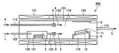
(実施形態1)
図1を参照して、本発明にかかるIII族窒化物結晶の製造方法の一実施形態は、図1(a)に示すように反応室110内にHClガス1を導入して反応室110内を洗浄する工程と、図1(b)に示すように洗浄された反応室110内でIII族窒化物結晶11を気相成長させる工程とを含む。(Embodiment 1)
Referring to FIG. 1, in one embodiment of a method for producing a group III nitride crystal according to the present invention,
図1(a)および(b)を参照して、発明者らは、III族窒化物結晶11の成長の際に反応室110内に堆積したIII族窒化物の多結晶から形成される堆積物9が、HClガス1によってエッチングされることを見出し、これを反応室110内の洗浄に用いることにより、本発明を完成させた。 Referring to FIGS. 1 (a) and (b), the inventors have determined that deposits formed from group III nitride polycrystals deposited in
たとえば、III族窒化物であるGaNは、以下の反応式(1)〜(3)のように、
GaN(s) + HCl(g) → GaCl(g) + (1/2)N2(g) + (1/2)H2(g) (1)
GaN(s) + 2HCl(g) → GaCl2(g) + (1/2)N2(g) + H2(g) (2)
GaN(s) + 3HCl(g) → GaCl3(g) + (1/2)N2(g) + (3/2)H2(g) (3)
HClガスと反応して、GaClガス、GaCl2ガスまたはGaCl3ガスとなって除去される。これは、GaN以外のAlNなどのIII族窒化物についても同様である。For example, GaN, which is a group III nitride, has the following reaction formulas (1) to (3):
GaN (s) + HCl (g) → GaCl (g) + (1/2) N2 (g) + (1/2) H2 (g) (1)
GaN (s) + 2HCl (g ) → GaCl 2 (g) + (1/2) N 2 (g) + H 2 (g) (2)
GaN (s) + 3HCl (g) → GaCl3 (g) + (1/2) N2 (g) + (3/2) H2 (g) (3)
It reacts with HCl gas to be removed as GaCl gas, GaCl2 gas or GaCl3 gas. The same applies to group III nitrides such as AlN other than GaN.
図1(b)を参照して、III族窒化物結晶を成長させる際に、反応室110内、特に原料導入部(III族元素原料ガス導入管123、窒素原料ガス導入管113およびHClガス導入管111の端部の近傍の部分であって主としてヒータ132によって加熱される部分をいう、以下同じ)および結晶成長部(結晶を成長させるための基板ホルダ119の近傍の部分であって主としてヒータ133によって加熱される部分をいう、以下同じ)に、III族窒化物の多結晶で形成される堆積物9が付着する。 Referring to FIG. 1B, when a group III nitride crystal is grown, in the
ここで、図1(a)を参照して、反応室110内にHClガス1を導入して反応室110内を洗浄する工程においては、HClガス導入管111を介して上記堆積物9が付着している反応室110内にHClガス1を導入する。ここで、HClガスを効率的に輸送したり、HClガスの分圧を調節するために、キャリアガスが併用される。キャリアガスとしては、H2ガス、N2ガス、Arガス、Heガスなどが用いられる。キャリアガスは、III族窒化物の多結晶で形成されている堆積物9の除去を促進する観点、あるいはコストの観点から、H2ガスが好ましい。堆積物9はHClガス1と反応して、III族元素塩化物ガス、N2ガスおよびH2ガスが生成する。かかるIII族元素塩化物ガス、N2ガスおよびH2ガスは、反応室110内からガス排出管115を介して排ガス5として排出され、反応室110内が洗浄される。ここでHClガス導入管111の開口部は、窒素原料ガス導入管113およびIII族元素原料ガス導入管123の先端部、つまり多結晶で形成される堆積物9が付着する領域よりも上流側にあることが好ましい。Here, referring to FIG. 1A, in the step of introducing the
次に、図1(b)を参照して、洗浄された反応室110内でIII族窒化物結晶11を気相成長させる工程は、以下のようにして行なわれる。HClガス1をHClガス導入管122を介してIII族元素原料ガス生成室120に導入する。III族元素原料ガス生成室120内には、III族元素2が入っているIII族元素ボート121が配置されており、III元素2はHClガス1と反応して、III族元素原料ガス3であるIII族元素塩化物ガスを生成する。 Next, referring to FIG. 1B, the step of vapor-phase-growing the group III
このIII族元素原料ガス3は、III族元素塩原料ガス生成室120からIII族元素原料ガス導入管123を介して反応室110内に導入される。また、窒素原料ガス4であるNH3ガスが、窒素原料ガス導入管113を介して反応室110内に導入される。反応室110内でIII族元素原料ガス3と窒素原料ガス4とが反応して結晶成長部の基板ホルダ119上に配置された下地基板10上にIII族窒化物結晶11が成長する。過剰のガスは排ガス5として、ガス排出管115を介して反応室110内から排出される。このとき、III族元素原料ガスおよび窒素原料ガスを効率的に輸送したり、各原料ガスの分圧を調節するために、キャリアガスが併用される。キャリアガスとしては、H2ガス、N2ガスなどが用いられる。The group III
このとき、上記のように、反応室110内、特に原料導入部およびに結晶成長部に、III族窒化物の多結晶で形成される堆積物9が付着する。III族元素原料ガス導入管123、窒素原料ガス導入管113およびHClガス導入管111の先端部に堆積物9が付着してしまうと、原料ガスの供給が阻害されるため、安定した品質の結晶を得ること、および長時間成長させて厚い結晶を得ることが困難となる。 At this time, as described above, the
したがって、さらに、上記の反応室内にHClガスを導入して反応室内を洗浄する工程、洗浄された反応室内でIII族窒化物結晶を気相成長させる工程を繰り返し行なうことにより、気相中で効率的に反応室の洗浄およびIII族窒化物結晶の成長を行うことができ、効率的に結晶性のよいIII族窒化物結晶が得られる。 Therefore, the process of cleaning the reaction chamber by introducing HCl gas into the reaction chamber and the step of vapor-phase-growing the group III nitride crystal in the cleaned reaction chamber are repeated to improve the efficiency in the gas phase. Thus, the reaction chamber can be cleaned and the group III nitride crystal can be grown, and a group III nitride crystal having good crystallinity can be obtained efficiently.
本実施形態のIII族窒化物結晶の製造方法において、反応室内を洗浄する工程は、HClガス分圧が1.013hPa以上1013hPa以下(0.001atm以上1atm以下)、反応室内温度が650℃以上1200℃以下の条件で行なうことが好ましい。HClガス分圧が1.013hPaより低いと堆積物9の除去効果が低減し、1013hPaより高いと導入されたHClガスを反応室内から排出することが困難となる。また、反応室内温度が650℃より低いと堆積物9の除去効果が低減し、1200℃より高いと反応室の劣化および/または損傷が起こる。かかる観点から、反応室内温度は800℃以上が好ましく、900℃以上がより好ましい。 In the method for producing a group III nitride crystal of the present embodiment, the step of cleaning the reaction chamber includes an HCl gas partial pressure of 1.013 hPa to 1013 hPa (0.001 atm to 1 atm), and a reaction chamber temperature of 650 ° C. to 1200 ° C. It is preferable to carry out under the conditions of not more than ° C. When the HCl gas partial pressure is lower than 1.013 hPa, the effect of removing the
本実施形態のIII族窒化物結晶の製造方法においては、洗浄された反応室内でIII族窒化物結晶を気相成長させる工程において、反応室内の原料導入部の温度を調節することにより、III族窒化物結晶中の酸素原子濃度およびケイ素原子濃度を調節することができる。 In the method for producing a group III nitride crystal of the present embodiment, in the step of vapor phase growth of the group III nitride crystal in the cleaned reaction chamber, the temperature of the raw material introduction part in the reaction chamber is adjusted to adjust the group III The oxygen atom concentration and silicon atom concentration in the nitride crystal can be adjusted.
反応室が石英などの酸素含有材料から形成されている場合は、III族窒化物結晶の成長の際に、反応室に含有される酸素原子およびケイ素原子がIII族窒化物結晶に混入する。たとえば、石英SiO2(s)に対してNH3(g)およびH2(g)が接触する系における石英の熱分解について、SiO2(s):NH3(g):H2(g)が1:10:40のモル比で存在し、NH3(g)およびH2(g)の全圧が1013hPa(1atm)の場合の熱力学的計算を行なうと、反応室内温度が上がるとともに水蒸気(すなわちH2O(g))およびSi系ガス(たとえばSi2N2O(g))が生成することがわかった。生成するH2O(g)およびSi系ガスの分圧は、それぞれ、600℃で0.41Pa(4×10⁻⁶atm)および0.10Pa(1×10⁻⁶atm)と、1000℃で2.43Pa(2.4×10⁻⁵atm)および0.61Pa(6×10⁻⁶atm)と、反応室内温度の上昇とともに増大する。この水蒸気中の酸素原子およびSi系ガス中のケイ素原子が不純物としてIII族窒化物結晶に取り込まれる。When the reaction chamber is formed of an oxygen-containing material such as quartz, oxygen atoms and silicon atoms contained in the reaction chamber are mixed into the group III nitride crystal during the growth of the group III nitride crystal. For example, the NH3 (g) and H2 (g) the pyrolysis of quartz in a system which is in contact against the quartzSiO 2 (s), SiO 2 (s): NH 3 (g): H 2 (g) Is present at a molar ratio of 1:10:40, and a thermodynamic calculation is performed when the total pressure of NH3 (g) and H2 (g) is 1013 hPa (1 atm), the temperature in the reaction chamber increases and water vapor increases. (Ie, H2 O (g)) and Si-based gas (eg, Si2 N2 O (g)) were produced. The partial pressures of H2 O (g) and Si-based gas produced are 0.41 Pa (4 × 10⁻⁶ atm) and 0.10 Pa (1 × 10⁻⁶ atm) at 1000 ° C. and 1000 ° C., respectively. It increases to 2.43 Pa (2.4 × 10⁻⁵ atm) and 0.61 Pa (6 × 10⁻⁶ atm) as the reaction chamber temperature increases. Oxygen atoms in the water vapor and silicon atoms in the Si-based gas are taken into the group III nitride crystal as impurities.
ここで、反応室内温度は、主に原料導入部および結晶成長部の温度を調節することにより調節される。結晶性のよいIII族窒化物結晶を安定して成長させる観点から、結晶成長部は1000〜1200℃程度に維持することが好ましい。したがって、酸素原子濃度およびケイ素原子濃度を制御するための反応室内温度の調節は、現実的には多くの場合、結晶成長部の温度調整ではなく、原料導入部の温度調節あるいは、反応室内部に石英製の部品を設置し、それを加熱することでH2OガスおよびSi2N2Oガスを発生させても構わない。また、結晶成長部とは、III族窒化物結晶を成長させる部分をいい、図1では反応室110においてヒータ133で加熱される部分をいう。Here, the temperature in the reaction chamber is adjusted mainly by adjusting the temperatures of the raw material introduction part and the crystal growth part. From the viewpoint of stably growing a group III nitride crystal having good crystallinity, the crystal growth part is preferably maintained at about 1000 to 1200 ° C. Therefore, in many cases, the adjustment of the temperature in the reaction chamber for controlling the oxygen atom concentration and the silicon atom concentration is actually not the temperature adjustment in the crystal growth portion but the temperature adjustment in the raw material introduction portion or in the reaction chamber. A quartz part may be installed and heated to generate H2 O gas and Si2 N2 O gas. Further, the crystal growth portion refers to a portion where a group III nitride crystal is grown, and in FIG. 1, refers to a portion heated by the
III族窒化物結晶としてGaN結晶を成長させる場合は、III族元素原料ガス生成室120内および原料導入部の温度を650℃以上1200℃以下の範囲で調節することが好ましい。III族元素原料ガス生成室120内の温度が650℃より低いと、HClガス1と金属Ga(III族元素2)との反応性が低下しGaClガス(III族元素原料ガス3)の反応室110への導入が困難となり、原料導入部の温度が1200℃より高いと石英部品などの劣化および/または損傷が起こりやすくなる。 When growing a GaN crystal as a group III nitride crystal, it is preferable to adjust the temperature in the group III element source
(実施形態2)
図1を参照して、本発明にかかるIII族窒化物結晶の製造装置の一実施形態(製造装置100)は、反応室110内に直接HClガス1を導入する構造とHVPE法によりIII族窒化物結晶を成長させる構造とを備える。反応室110内に直接HClガス1を導入する構造を備えることにより、III族窒化物結晶11を成長させた際に反応室110内に付着したIII族窒化物の多結晶で形成される堆積物9を気相中で効率的に除去することができる。(Embodiment 2)
Referring to FIG. 1, an embodiment (production apparatus 100) of a group III nitride crystal production apparatus according to the present invention has a structure in which
本実施形態のIII族窒化物結晶の製造装置100は、上記堆積物9を除去するために、反応室110内に直接HClガス1を導入する構造を備える。反応室内に直接HClガスを導入する構造には、特に制限はないが、たとえば、図1を参照して、HClガス1を直接反応室110内に導入するためのHClガス導入管110が挙げられる。本実施形態のIII族窒化物結晶の製造装置は、HClガス1を直接反応室110内に導入するためのHClガス導入管110が配設されているため、反応室110内の堆積物9を効率的に除去することができる。 The III-nitride
また、本実施形態のIII族窒化物結晶の製造装置は、HVPE法によりIII族窒化物結晶を成長させる構造を備える。ここで、HVPE法とは、III族元素原料ガスであるIII族元素塩化物ガスと、窒素原料ガスであるNH3ガスとを反応させて、気相でIII族窒化物結晶を成長させる方法をいう。また、HVPE法により結晶を成長させる装置をHVPE装置とよぶ。In addition, the group III nitride crystal manufacturing apparatus of this embodiment includes a structure for growing a group III nitride crystal by the HVPE method. Here, the HVPE method is a method of growing a group III nitride crystal in a gas phase by reacting a group III element chloride gas that is a group III element source gas and an NH3 gas that is a nitrogen source gas. Say. An apparatus for growing crystals by the HVPE method is called an HVPE apparatus.
たとえば、図1を参照して、本実施形態のIII族窒化物結晶の製造装置100には、反応室110、III族元素原料ガス生成室120、ならびに反応室110およびIII族元素原料ガス生成室120を加熱するためのヒータ131,132,133を備える。反応室110およびIII族元素原料ガス生成室120には、HClガス1をIII族元素原料ガス生成室120に導入するためのHClガス導入管122が配設されている。III族元素原料ガス生成室120には、その内部にIII族元素2を入れるIII族元素ボート121が配置され、生成されたIII族元素原料ガス3を反応室110に導入するためのIII族元素原料ガス導入管123が配設されている。反応室110には、窒素原料ガス4を反応室110内に導入するための窒素原料ガス導入管113および排ガス5を反応室110から排出するためのガス排出管115が配設されている。また、反応室110内には、III族窒化物結晶11を成長させるための下地基板10を配置するための基板ホルダ119が配置されている。反応室110を形成する反応管101には、特には制限はないが、大きな反応管が容易に作製できる観点から、石英反応管が好ましく用いられる。 For example, referring to FIG. 1, group III nitride
ここで、成長時あるいはエッチング時には、副生成物として、塩化アンモニウム(NH4Cl)粉末が生成する。この粉末は、ガス排出管115を詰まらせ、長時間の結晶成長、つまり厚い結晶を得ることを阻害する要因となるため、ガス排出管115の入口部115aおよび/または出口部115bに、塩化アンモニウムをトラップする装置(トラップ装置116)を取り付けることが好ましい。塩化アンモニウムは、約340℃以下でHClとNH3が存在すると生成する。その形態は粉末状である。そこで、トラップ装置116内は空冷でも水冷でもよいが、冷却することが好ましい。メンテナンスのし易さから、空冷であることが好ましい。トラップ装置116には、フィルター116fが内蔵されていてもよい。また、トラップ装置116は、ガスの入口と出口が装置の上部にあり、装置の下部は塩化アンモニウム粉末が蓄積されるように深くなっていると、ガスの入口と出口が詰まりにくいため好ましい。Here, during growth or etching, ammonium chloride (NH4 Cl) powder is generated as a by-product. Since this powder clogs the
(実施形態3)
図2を参照して、本発明にかかるIII族窒化物結晶の製造装置の他の実施形態(製造装置200)は、図1の実施形態2におけるIII族窒化物結晶の製造装置100の反応室110の結晶成長部に反応室110の保護部材117が配置されている。保護材117は、図2のように反応室110となる反応管101の内壁に密着させてもよいし、反応管101の内壁から離してもよい。(Embodiment 3)
Referring to FIG. 2, another embodiment (manufacturing apparatus 200) of a group III nitride crystal manufacturing apparatus according to the present invention is a reaction chamber of group III nitride
反応室110の結晶成長部では結晶成長の際に1000℃〜1200℃程度の高温となる。したがって、結晶成長部付近の反応管101の内壁も、結晶成長部と同程度の温度となり、結晶が生成しやすい環境となるため、結晶成長部付近の反応管101の内壁にも多結晶のIII族窒化物(たとえば、GaN結晶を成長させる場合は多結晶GaN、AlN結晶を成長させる場合は多結晶AlN)が多く付着する。また、反応管101が石英などの酸素含有材料で形成されている場合は、窒素原料ガスであるNH3ガスおよび/またはキャリアガスであるH2ガスと反応して、水蒸気を生成してIII族窒化物結晶に酸素原子が混入するとともに、反応管101を劣化させ損傷させる。In the crystal growth part of the
反応室110の結晶成長部に反応管101の保護部材117を配置することにより、結晶成長部における反応管101を形成する石英と原料ガスおよび/または水素ガスとの接触を抑制することができ、結晶成長部付近の反応管101の内壁への多結晶のIII族窒化物の付着を抑制することができる上、反応管101の劣化および損傷を抑制することができる。また、この反応管101の結晶成長部における石英(SiO2)が分解しても、III族窒化物結晶成長部とSiO2分解領域が保護材117で分断されているため、酸素原子およびケイ素原子を含んだガスが結晶成長部へとは行かず、III族窒化物結晶11への酸素原子およびケイ素原子の混入、反応管101の劣化および損傷を抑制することができる。保護部材117には、特に制限はないが、III族窒化物結晶への酸素原子の混入、反応管101の劣化および損傷を抑制する観点から、pBN(熱分解窒化ホウ素)、カーボン、SiC、WC、TaCなどの酸化物以外の材料などで形成されていることが好ましい。なお、ガス排出管115の入口部115aおよび/または出口部115bにトラップ装置116が取り付けられていることが好ましく、また、このトラップ装置116にフィルタ116fが含まれていてもよいことは、実施形態2の場合と同様である。By disposing the
(実施形態4)
図3を参照して、本発明にかかるIII族窒化物結晶の製造方法の他の実施形態は、反応室110内を洗浄する工程において、III族元素原料ガス生成室120およびIII族元素原料ガス導入管123を、製造装置300の反応室110から取り外した後、HClガス導入管122を介して反応室110内にHClガスを導入することにより、反応室110内を洗浄する実施形態である。なお、取り外されたIII族元素原料ガス生成室120およびIII族元素原料ガス導入管123は、別途、HClガスによる気相エッチング、リン酸、硫酸などによる液相エッチングなどにより、洗浄される。(Embodiment 4)
Referring to FIG. 3, in another embodiment of the method for producing a group III nitride crystal according to the present invention, in the step of cleaning the inside of
次に、洗浄されたIII族元素原料ガス生成室120およびIII族元素原料ガス導入管123を、洗浄された反応室110に再び取り付けた後、この洗浄された反応室110内でIII族窒化物結晶を成長させる。 Next, the cleaned group III element source
本実施形態における反応室内を洗浄する工程によれば、III族窒化物結晶を成長させる工程の際にはIII族元素原料ガス生成室にHClガスを導入するHClガス導入管122を用いて、反応室110に直接HClガス1を導入することができる。このため、図1の製造装置100に示すような反応室110に直接HClガス1を導入するためのHClガス導入管111を設ける必要がない。しかし、III族元素原料ガス生成室120およびIII族元素原料ガス導入管123を別途洗浄する必要がある。なお、本実施形態において用いられる製造装置300において、ガス排出管115の入口部115aおよび/または出口部115bにトラップ装置116が取り付けられていることが好ましく、また、このトラップ装置116にフィルタ116fが含まれていてもよいことは、実施形態2の場合と同様である。 According to the step of cleaning the reaction chamber in this embodiment, the reaction is performed using the HCl
なお、上記実施形態1〜4においては、HVPE法における本発明の実施形態を説明したが、本発明は、HVPE法以外の各種気相成長方法、たとえばMOC法、MOCVD法に好ましく適用することができる。ここで、MOC法とは、III族元素原料ガスとして、III族元素の有機金属化合物ガスとHClガスとを反応させてIII族元素塩化物ガスを生成させ、このIII族元素塩化物ガスと窒素原料ガスであるNH3ガスとを反応させて、気相でIII族窒化物結晶を成長させる方法である。また、MOCVD法とは、III族元素原料ガスであるIII族元素の有機金属化合物ガスと窒素原料ガスであるNH3ガスとを反応させて、気相でIII族窒化物結晶を成長させる方法である。In the first to fourth embodiments, the embodiment of the present invention in the HVPE method has been described. However, the present invention is preferably applied to various vapor phase growth methods other than the HVPE method, for example, the MOC method and the MOCVD method. it can. Here, the MOC method is a group III element source gas which is a group III element organic metal compound gas and HCl gas reacted to generate a group III element chloride gas. In this method, a group III nitride crystal is grown in a gas phase by reacting with a source gas, NH3 gas. The MOCVD method is a method of growing a group III nitride crystal in a gas phase by reacting a group III element organometallic compound gas which is a group III element source gas and an NH3 gas which is a nitrogen source gas. is there.
(比較例1)
図4に示す従来のIII族窒化物結晶の製造装置400を用いてGaN結晶を成長させた。なお、この製造装置400には、ガス排出管115に塩化アンモニウムをトラップする装置(トラップ装置)を設けずに成長を行なった。まず、反応室110となる新品の石英反応管101を製造装置400にセットした後、この石英反応管101内に付着した水分などの不純物を除去するため、反応室110内にN2ガスを流しながら1050℃で50時間の空焼きを行なった。(Comparative Example 1)
A GaN crystal was grown using the conventional group III nitride
その後、反応室110内に下地基板10として直径50.8mmの(0001)サファイア基板(結晶成長面が(0001)面であるサファイア基板をいう、以下同じ)をセットした後、反応室110内のIII族元素原料ガス生成室120内および原料導入部の温度を850℃、結晶成長部の温度を1030℃として、HClガス分圧(GaClガス分圧)20.26hPa(0.02atm)、NH3ガス分圧303.9hPa(0.3atm)で15時間、下地基板10上にGaN結晶(III族窒化物結晶11)を成長させた(1回目の結晶成長)。以下、比較例ならびに実施例においては直径50.8mmの基板を使用して成長を実施した。得られたGaN結晶は、厚さが約1.7mmで、茶色透明であり、その表面に凹凸が見られた。また、得られたGaN結晶の外周部には、多結晶GaNが付着していた。After that, a (0001) sapphire substrate having a diameter of 50.8 mm (referred to as a sapphire substrate having a crystal growth surface of (0001) plane, hereinafter the same) is set as the
このGaN結晶の外周部の多結晶GaNを外周研削で削り落とした後、表面を研削および研磨して平滑にした。かかる外周研削、表面研削、研磨の過程ではクラックは観察できなかった。このGaN結晶の平滑にされた表面を、蛍光顕微鏡を用いて可視光観察したところ、明るい領域と暗い領域とが見られた。ここで、暗い領域は(11−22)面などのファセットで成長した領域(以下、ファセット成長領域という)を示し、明るい領域は(0001)面で成長した領域(以下、C面成長領域という)を示す。結晶成長において、ファセット成長領域とC面成長領域とを共存させることにより、ファセットにより形成される凹状のピット部の頂点から結晶内にC面対して垂直に結晶内に伸びる領域に転位を集めることができ、この転位集中領域以外の領域の転位密度を低減することができる。なお、かかるファセット成長領域は、結晶成長温度を低くするほど、また、III族元素原料ガスの分圧に対する窒素原料ガスの分圧の比を低くするほど、形成されやすい。 After the polycrystalline GaN on the outer peripheral portion of the GaN crystal was scraped off by outer peripheral grinding, the surface was ground and polished to be smooth. No cracks could be observed during the process of peripheral grinding, surface grinding, and polishing. When the smoothed surface of the GaN crystal was observed with visible light using a fluorescence microscope, a bright region and a dark region were observed. Here, a dark region indicates a region grown with facets such as the (11-22) plane (hereinafter referred to as a facet growth region), and a bright region indicates a region grown with the (0001) plane (hereinafter referred to as a C-plane growth region). Indicates. In crystal growth, by allowing a facet growth region and a C-plane growth region to coexist, dislocations are collected from the apex of the concave pit portion formed by the facet to a region extending in the crystal perpendicular to the C-plane in the crystal. The dislocation density in the region other than the dislocation concentration region can be reduced. Such facet growth regions are more easily formed as the crystal growth temperature is lowered and the ratio of the partial pressure of the nitrogen source gas to the partial pressure of the group III element source gas is lowered.
GaN結晶のファセット成長領域の不純物濃度をSIMS(Secondary Ion Mass Spectroscopy;2次イオン質量分析法)によって測定したところ、不純物としてH原子、C原子、Si原子およびO原子が観察された。H原子、C原子およびSi原子の濃度はいずれも1.0×1017cm-3未満であった。また、O原子濃度は1.2×1019cm-3であった。また、GaN結晶のC面成長領域の不純物濃度は、O原子、H原子およびC原子の濃度はいずれも1.0×1017cm-3未満であり、Si原子濃度は1.0×1018cm-3であった。When the impurity concentration in the facet growth region of the GaN crystal was measured by SIMS (Secondary Ion Mass Spectroscopy), H atoms, C atoms, Si atoms, and O atoms were observed as impurities. The concentrations of H atom, C atom and Si atom were all less than 1.0 × 1017 cm−3 . The O atom concentration was 1.2 × 1019 cm−3 . The impurity concentration in the C-plane growth region of the GaN crystal is such that the concentrations of O atoms, H atoms, and C atoms are all less than 1.0 × 1017 cm−3 , and the Si atom concentration is 1.0 × 10¹⁸. cm-3 .
このGaN結晶を成長させた後の反応室110内、特に、結晶成長部および原料導入部(特に、III族元素原料ガス導入管123、窒素原料ガス導入管113およびHClガス導入管111の端部、実施例および比較例において以下同じ)にGaNの多結晶で形成されている堆積物9が、厚さ0.3〜0.7mm程度で付着していた。さらに、ガス排出管115の内壁には塩化アンモニウムが厚さ2〜4mm程度で堆積していた。 In the
この石英反応管101を反応室110として用いて、再度、1回目の結晶成長と同じ条件でGaN結晶を成長させた(2回目の結晶成長)。得られたGaN結晶は、厚さが約1mm程度と1回目に成長させたGaN結晶よりも厚さが薄く、茶色透明であり、その表面に凸凹が見られた。また、得られたGaN結晶の外周部には、多結晶GaNが付着していた。このGaN結晶のファセット成長領域のO原子濃度およびSi原子濃度はそれぞれ1.2×1019cm-3および1.0×1017cm-3未満であり、C面成長領域のO原子濃度およびSi原子濃度はそれぞれ1.0×1017cm-3未満および1.0×1018cm-3であった。また、評価するにあたり、上記同様の加工を実施したが、クラックは観察できなかった。この2回目の結晶成長後の反応室110内、特に、結晶成長部および原料導入部にGaNの多結晶で形成されている堆積物9の厚さは、1.1〜2.4mmとなった。すなわち、2回目の結晶成長の際に、1回目結晶成長の際の倍以上の厚さの堆積物が付着したものと考えられる。また、2回目の結晶成長の際、ガス排出管115の内壁には、1回目の結晶成長に比べて、倍以上の厚さの塩化アンモニウムが堆積していた。すなわち、2回目の結晶成長においては、1回目の結晶成長に比べて、より多くのGa原料および窒素原料が堆積物9となり、さらにはガス排出管115が詰まってきたことにより、GaN結晶の成長効率が低減していることがわかる。Using this
(比較例2)
比較例1における2回目の結晶成長後の反応室110内に厚さが1.1〜2.4mm程度の堆積物9が付着しており、ガス排出管115内に厚さ5〜10mm程度の塩化アンモニウムが付着していた。この堆積物9が付着した石英反応管101を製造装置400から取り出して、モル比1:1の燐酸と硫酸との混合溶液(液温180℃)中に浸漬して、24時間エッチングすることにより石英反応管の洗浄を行なった(液相エッチングによる洗浄)。その結果、残存していた堆積物においてエッチング前の厚さ2.4mmがエッチング後の厚さ1.0mmとなった。このことから、この堆積物のエッチング速度は、約60μm/hrと見積もることができた。そこで、この堆積物が残存している石英反応管101を同条件でさらに24時間エッチングを行ない、残存している堆積物を除去した。さらに、塩化アンモニウムが付着しているガス排出管115を水で洗浄して、付着している塩化アンモニウムを除去した。(Comparative Example 2)
上記のようにして洗浄された石英反応管101を反応室110として製造装置400にセットした後、この石英反応管101内に付着した水分を除去するため、反応室110内にN2ガスを流しながら1050℃で50時間の空焼きを行なった。After the
その後、反応室110内に下地基板10として(0001)サファイア基板をセットした後、反応室110内のIII族元素原料ガス生成室120および原料導入部の温度を850℃、結晶成長部の温度を1030℃として、HClガス分圧(GaClガス分圧)20.26hPa(0.02atm)、NH3ガス分圧303.9hPa(0.3atm)で15時間、下地基板10上にGaN結晶(III族窒化物結晶11)を成長させた。Then, after setting a (0001) sapphire substrate as the
得られたGaN結晶は、厚さが約1.7mmで、比較例1において成長させたGaN結晶より濃い茶色透明であり、その表面に凹凸が見られた。また、得られたGaN結晶の外周部には、多結晶GaNが付着しており、多結晶部と単結晶部の界面に長さが数十から数百μm程度のクラックが観察された。酸素濃度分析を実施するため、比較例1と同様な加工処理を実施したにもかかわらず、加工後の結晶には、加工前に見られたクラック以外場所に、長さが数十から数百μm程度の微細なクラックが観察できた。微細なクラックを避けてGaN結晶の不純物濃度を評価した。このGaN結晶にはファセット成長領域とC面成長領域とが含まれ、ファセット成長領域のO原子濃度およびSi原子濃度はそれぞれ3.5×1019cm-3および1.0×1017cm-3未満であり、C面成長領域のO原子濃度およびSi原子濃度はそれぞれ1.0×1017cm-3未満および2.0×1018cm-3であった。このGaN結晶の不純物である酸素原子の濃度が、比較例1において成長させたGaN結晶の不純物である酸素原子の濃度よりも高かったことから、本比較例のような液相エッチングによる洗浄の場合は、1050℃で50時間程度の空焼きでは充分でないと考えられる。また、比較例1では観察できなかったクラックが発生したことから、酸素濃度が高くなると不純物硬化によって、結晶がもろくなったと考えられる。The obtained GaN crystal had a thickness of about 1.7 mm and was darker brown and transparent than the GaN crystal grown in Comparative Example 1, and irregularities were observed on the surface thereof. In addition, polycrystalline GaN adhered to the outer peripheral portion of the obtained GaN crystal, and cracks having a length of about several tens to several hundred μm were observed at the interface between the polycrystalline portion and the single crystal portion. In order to perform the oxygen concentration analysis, despite the processing similar to that in Comparative Example 1, the crystal after processing has a length of several tens to several hundreds in places other than the cracks observed before processing. A fine crack of about μm could be observed. The impurity concentration of the GaN crystal was evaluated avoiding fine cracks. This GaN crystal includes a facet growth region and a C-plane growth region, and the O atom concentration and the Si atom concentration in the facet growth region are 3.5 × 1019 cm−3 and 1.0 × 1017 cm−3, respectively. The O atom concentration and the Si atom concentration in the C-plane growth region were less than 1.0 × 1017 cm−3 and 2.0 × 1018 cm−3 , respectively. In the case of cleaning by liquid phase etching as in this comparative example, the concentration of oxygen atoms as impurities in the GaN crystal was higher than the concentration of oxygen atoms as impurities in the GaN crystal grown in Comparative Example 1. Is considered to be insufficient for baking at 1050 ° C. for about 50 hours. In addition, since cracks that could not be observed in Comparative Example 1 occurred, it was considered that the crystals became brittle due to impurity curing when the oxygen concentration was increased.
(実施例1)
図1に示す本発明にかかるIII族窒化物結晶の製造装置100を用いてGaN結晶を成長させた。なお、この製造装置100には、塩化アンモニウムをトラップする装置(トラップ装置116)は設けずに成長を行なった。まず、反応室110となる新品の石英反応管101を製造装置100にセットした後、この石英反応管101内に付着した水分などの不純物を除去するため、反応室110内にN2ガスを流しながら反応室内温度1050℃で50時間の空焼きを行なった。その後、反応室110内に下地基板10として直径50.8mmの(0001)サファイア基板をセットした後、反応室110内のIII族元素原料ガス生成室120および原料導入部の温度を850℃、結晶成長部の温度を1030℃として、HClガス分圧(GaClガス分圧)20.26hPa(0.02atm)、NH3ガス分圧303.9hPa(0.3atm)で15時間、下地基板10上にGaN結晶(III族窒化物結晶11)を成長させた。得られたGaN結晶にはファセット成長領域とC面成長領域とが含まれ、ファセット成長領域のO原子濃度およびSi原子濃度はそれぞれ1.2×1019cm-3および1.0×1017cm-3未満であり、C面成長領域のO原子濃度およびSi原子濃度はそれぞれ1.0×1017cm-3未満および1.0×1018cm-3であった。Example 1
A GaN crystal was grown using the group III nitride
このGaN結晶を成長させた後の反応室110内、特に、結晶成長部および原料導入部にGaNの多結晶で形成されている堆積物9が、厚さ0.3〜0.7mm程度で付着していた。さらに、ガス排出管115の内壁には塩化アンモニウムが厚さ2〜4mm程度で堆積していた。 The
この堆積物9が付着した反応室110内に、HClガス導入管111を介してHClガス1およびH2ガス(キャリアガス)を導入して、反応室内温度1000℃で5時間エッチングすることにより、反応室110内を洗浄した(気相エッチングによる洗浄)。ここで、HClガス1の分圧は50.65hPa(0.05atm)とした。その結果、反応室110内の堆積物9は気相エッチングにより全て除去された。また、別の気相エッチング実験から、本条件における堆積物9のエッチング速度は約500μm/hrと見積もることができた。なお、ガス排出管115には、塩化アンモニウムが付着していた。By introducing
その後、反応室110内に下地基板10として(0001)サファイア基板をセットした後、反応室110内のIII族元素原料ガス生成室120および原料導入部の温度を850℃、結晶成長部の温度を1030℃として、HClガス分圧(GaClガス分圧)20.26hPa(0.02atm)、NH3ガス分圧303.9hPa(0.3atm)で15時間、下地基板10上にGaN結晶(III族窒化物結晶11)を成長させた。Then, after setting a (0001) sapphire substrate as the
得られたGaN結晶は、厚さが約1.7mmで、比較例1および比較例2において成長させたGaN結晶より淡い茶色透明であり、その表面に凹凸が見られた。また、比較例と同様にGaN結晶の外周部には多結晶GaNが付着していた。比較例と同様の加工ならびに測定を実施した結果、このGaN結晶のファセット成長領域のO原子濃度およびSi原子濃度はそれぞれ6.6×1018cm-3および1.0×1017cm-3未満であり、C面成長領域のO原子濃度およびSi原子濃度はそれぞれ1.0×1017cm-3未満および6.5×1017cm-3であった。また、成長後、加工後においてクラックは観察できなかった。The obtained GaN crystal had a thickness of about 1.7 mm and was lighter brown and transparent than the GaN crystals grown in Comparative Example 1 and Comparative Example 2, and unevenness was observed on the surface thereof. Further, as in the comparative example, polycrystalline GaN adhered to the outer peripheral portion of the GaN crystal. As a result of performing the same processing and measurement as in the comparative example, the O atom concentration and the Si atom concentration in the facet growth region of the GaN crystal were less than 6.6 × 1018 cm−3 and 1.0 × 1017 cm−3, respectively. The O atom concentration and the Si atom concentration in the C-plane growth region were less than 1.0 × 1017 cm−3 and 6.5 × 1017 cm−3 , respectively. In addition, no cracks could be observed after growth and after processing.
(実施例2)
実施例1のGaN結晶成長後の反応室110内を観察したところ、GaNの多結晶で形成されている厚さ0.3〜0.7mm程度の堆積物9が付着していた。この堆積物9が付着した反応室110内を、キャリアガスとしてN2ガスを用いて、HClガス分圧50.65hPa(0.05atm)、反応室内温度1000℃で5時間気相エッチングすることにより洗浄したところ、堆積物9は全て除去された。また、別の気相エッチング実験から、本条件における堆積物9のエッチング速度は約200μm/hrと見積もることができた。実施例1と比較してエッチング速度が低下した理由は、キャリアガスとしてN2ガスを用いたことで、窒素ガス分圧が上がり、堆積物9を形成する多結晶のGaNからの窒素の抜けおよび分解が抑制されたためと考えられる。(Example 2)
When the inside of the
その後、ガス排出管115の入口部115aに、塩化アンモニウムをトラップする装置(トラップ装置116)を取り付けた。取り付けたトラップ装置116は、SUS製の容器であり、容器内に塩化アンモニウムが溜まるように設計されている。次に、反応室110内に下地基板10として(0001)サファイア基板をセットした後、反応室110内のIII族元素原料ガス生成室120および原料導入部の温度を850℃、結晶成長部の温度を1030℃として、HClガス分圧(GaClガス分圧)20.26hPa(0.02atm)、NH3ガス分圧303.9hPa(0.3atm)で15時間、下地基板10上にGaN結晶(III族窒化物結晶11)を成長させた。Thereafter, a device for trapping ammonium chloride (trap device 116) was attached to the
得られたGaN結晶は、厚さが約1.7mmで、比較例1および比較例2において成長させたGaN結晶より淡い茶色透明であり、その表面に凹凸が見られた。また、比較例と同様にGaN結晶の外周部には多結晶GaNが付着していた。比較例と同様の加工ならびに測定を実施した結果、このGaN結晶にはファセット成長領域とC面成長領域とが含まれ、ファセット成長領域のO原子濃度およびSi原子濃度はそれぞれ6.2×1018cm-3および1.0×1017cm-3未満であり、C面成長領域のO原子濃度およびSi原子濃度はそれぞれ1.0×1017cm-3未満および6.3×1017cm-3であった。また、成長後、加工後においてクラックは観察できなかった。また、トラップ装置116を取り外してみると、トラップ装置116内に塩化アンモニウムが溜まっている一方、ガス排出管115には塩化アンモニウムが薄く(厚さが0.1〜0.2mm程度)付着しているだけで、ガス排出管115が詰まる様子は全く見受けられなかった。The obtained GaN crystal had a thickness of about 1.7 mm and was lighter brown and transparent than the GaN crystals grown in Comparative Example 1 and Comparative Example 2, and unevenness was observed on the surface thereof. Further, as in the comparative example, polycrystalline GaN adhered to the outer peripheral portion of the GaN crystal. As a result of performing the same processing and measurement as in the comparative example, this GaN crystal includes a facet growth region and a C-plane growth region, and the O atom concentration and the Si atom concentration in the facet growth region are 6.2 × 10¹⁸, respectively. cm−3 and 1.0 × 1017 cm−3 , and the O atom concentration and the Si atom concentration in the C-plane growth region are less than 1.0 × 1017 cm−3 and 6.3 × 1017 cm−, respectively. It was3 . In addition, no cracks could be observed after growth and after processing. Further, when the
(実施例3)
実施例2のGaN結晶成長後の反応室110内を観察したところ、GaNの多結晶で形成されている厚さ0.3〜0.7mm程度の堆積物9が付着していた。この堆積物9が付着した反応室110内を、キャリアガスとしてH2ガスを用いて、HClガス分圧50.65hPa(0.05atm)、反応室内温度850℃で8時間気相エッチングすることにより洗浄したところ、堆積物9は全て除去された。また、別の気相エッチング実験から、本条件における堆積物9のエッチング速度は約100μm/hrと見積もることができた。(Example 3)
When the inside of the
その後、反応室110内に下地基板10として(0001)サファイア基板をセットした後、反応室110内のIII族元素原料ガス生成室120および原料導入部の温度を850℃、結晶成長部の温度を1030℃として、HClガス分圧(GaClガス分圧)20.26hPa(0.02atm)、NH3ガス分圧303.9hPa(0.3atm)で15時間、下地基板10上にGaN結晶(III族窒化物結晶11)を成長させた。Then, after setting a (0001) sapphire substrate as the
得られたGaN結晶は、厚さが約1.7mmで、比較例1および比較例2において成長させたGaN結晶より淡い茶色透明であり、その表面に凹凸が見られた。また、比較例と同様にGaN結晶の外周部には多結晶GaNが付着していた。比較例と同様の加工ならびに測定を実施した結果、このGaN結晶にはファセット成長領域とC面成長領域とが含まれ、ファセット成長領域のO原子濃度およびSi原子濃度はそれぞれ6.0×1018cm-3および1.0×1017cm-3未満であり、C面成長領域のO原子濃度およびSi原子濃度はそれぞれ1.0×1017cm-3未満および6.2×1017cm-3であった。また、成長後、加工後においてクラックは観察できなかった。The obtained GaN crystal had a thickness of about 1.7 mm and was lighter brown and transparent than the GaN crystals grown in Comparative Example 1 and Comparative Example 2, and unevenness was observed on the surface thereof. Further, as in the comparative example, polycrystalline GaN adhered to the outer peripheral portion of the GaN crystal. As a result of performing the same processing and measurement as in the comparative example, this GaN crystal includes a facet growth region and a C-plane growth region, and the O atom concentration and the Si atom concentration in the facet growth region are 6.0 × 10¹⁸, respectively. cm−3 and 1.0 × 1017 cm−3 , and the O atom concentration and Si atom concentration in the C-plane growth region are less than 1.0 × 1017 cm−3 and 6.2 × 1017 cm−, respectively. It was3 . In addition, no cracks could be observed after growth and after processing.
ここで、上記実施例1、2および3に示すように、GaN結晶中の不純物である酸素原子の濃度は、結晶成長の回数を重ねるほど、若干低下する傾向が見られた。これは、使用した石英反応管101内のH2OあるいはCOなどの酸素原子を含む不純物が少しずつ減少しているため、および/または、石英反応管の内壁面は、使用開始時には微細な凹凸がありNH3などの窒素原料ガスとの反応面積が大きかったのに対し、使用を続けることで、内壁面の表面が、エッチングおよび/または高温雰囲気により滑らかになり、窒素原料ガスと反応する面積が減少しているためと考えられる。Here, as shown in Examples 1, 2 and 3, the concentration of oxygen atoms as impurities in the GaN crystal tended to decrease slightly as the number of crystal growths increased. This is because impurities including oxygen atoms such as H2 O or CO in the
また、実施例1、2および3で得られたGaN結晶について、ホール測定を室温(25℃)で実施したところ、SIMSで得られた酸素濃度と、ホール測定で測定したキャリア濃度がほぼ一致しており、これらのGaN結晶のキャリアは、この結晶中の不純物である酸素原子に関係したものであることがわかった。 In addition, when the hole measurement was performed at room temperature (25 ° C.) for the GaN crystals obtained in Examples 1, 2, and 3, the oxygen concentration obtained by SIMS and the carrier concentration measured by the hole measurement almost coincided. These GaN crystal carriers were found to be related to oxygen atoms as impurities in the crystal.
(実施例4)
図1に示す本発明にかかるIII族窒化物結晶の製造装置100を用いてGaN結晶を成長させた。まず、反応室110となる新品の石英反応管101を製造装置100にセットした後、この石英反応管101内に付着した水分などの不純物を除去するため、反応室110内にN2ガスを流しながら1050℃で50時間の空焼きを行なった。その後、反応室110内に下地基板10として(0001)サファイア基板をセットした後、反応室110内のIII族元素原料ガス生成室120およびGa原料導入部の温度を850℃、結晶成長部の温度を1030℃として、HClガス分圧(GaClガス分圧)20.26hPa(0.02atm)、NH3ガス分圧303.9hPa(0.3atm)で15時間、下地基板10上にGaN結晶(III族窒化物結晶11)を成長させた。得られたGaN結晶にはファセット成長領域とC面成長領域とが含まれ、ファセット成長領域のO原子濃度およびSi原子濃度はそれぞれ1.2×1019cm-3および1.0×1017cm-3未満であり、C面成長領域のO原子濃度およびSi原子濃度はそれぞれ1.0×1017cm-3未満および6.9×1017cm-3であった。Example 4
A GaN crystal was grown using the group III nitride
このGaN結晶を成長させた後の反応室110内、特に、結晶成長部および原料導入部にGaNの多結晶で形成されている堆積物9が、厚さ0.3〜0.7mm程度で付着していた。 The
この堆積物9が付着した反応室110内に、HClガス導入管111を介してHClガス1およびH2ガス(キャリアガス)を導入して、反応室内温度800℃で10時間エッチングすることにより、反応室110内を洗浄した(気相エッチングによる洗浄)。ここで、HClガス1の分圧は50.65hPa(0.05atm)とした。その結果、反応室110内の堆積物9は気相エッチングにより全て除去された。また、別の気相エッチング実験から、本条件における堆積物9のエッチング速度は約80μm/hrと見積もることができた。By introducing
その後、反応室110内に下地基板10として(0001)サファイア基板をセットした後、反応室110内のIII族元素原料ガス生成室120および原料導入部の温度を650℃、結晶成長部の温度を1030℃として、HClガス分圧(GaClガス分圧)20.26hPa(0.02atm)、NH3ガス分圧303.9hPa(0.3atm)で15時間、下地基板10上にGaN結晶(III族窒化物結晶11)を成長させた。Thereafter, after setting a (0001) sapphire substrate as the
得られたGaN結晶は、厚さが約1.5mmで、比較例1および比較例2において成長させたGaN結晶より淡い茶色透明であり、その表面に凹凸が見られた。また、比較例と同様にGaN結晶の外周部には多結晶GaNが付着していた。比較例と同様の加工ならびに測定を実施した結果、このGaN結晶にはファセット成長領域とC面成長領域とが含まれ、ファセット成長領域のO原子濃度およびSi原子濃度はそれぞれ5.3×1018cm-3および1.0×1017cm-3未満であり、C面成長領域のO原子濃度およびSi原子濃度はそれぞれ1.0×1017cm-3未満および6.7×1017cm-3であった。また、成長後、加工後においてクラックは観察できなかった。これまでの実施例と比較して、本実施例で得られたGaN結晶の厚みが薄い理由は、III族元素原料ガス生成室の温度を650℃としたことで、GaClガスの生成効率が低下したためと考えられるが、結晶品質ならびに製造上で問題はない。The obtained GaN crystal had a thickness of about 1.5 mm and was lighter brown and transparent than the GaN crystals grown in Comparative Example 1 and Comparative Example 2, and irregularities were observed on the surface thereof. Further, as in the comparative example, polycrystalline GaN adhered to the outer peripheral portion of the GaN crystal. As a result of performing the same processing and measurement as in the comparative example, this GaN crystal includes a facet growth region and a C-plane growth region, and the O atom concentration and the Si atom concentration in the facet growth region are 5.3 × 10¹⁸, respectively. cm−3 and 1.0 × 1017 cm−3 , and the O atom concentration and Si atom concentration in the C-plane growth region are less than 1.0 × 1017 cm−3 and 6.7 × 1017 cm−, respectively. It was3 . In addition, no cracks could be observed after growth and after processing. Compared with the previous examples, the reason why the thickness of the GaN crystal obtained in this example is thin is that the temperature of the group III element source gas generation chamber is set to 650 ° C., which reduces the generation efficiency of GaCl gas. This is probably because there is no problem in crystal quality and production.
(実施例5)
実施例4のGaN結晶成長後の反応室110内を観察したところ、GaNの多結晶で形成されている厚さ0.3〜0.7mm程度の堆積物9が付着していた。この堆積物9が付着した反応室110内を、キャリアガスとしてH2ガスを用いて、HClガス分圧50.65hPa(0.05atm)、反応室内温度700℃で15時間気相エッチングすることにより洗浄したところ、堆積物9は全て除去された。また、別の気相エッチング実験から、本条件における堆積物9のエッチング速度は約50μm/hrと見積もることができた。(Example 5)
When the inside of the
その後、反応室110内に下地基板10として(0001)サファイア基板をセットした後、反応室110内のIII族元素原料ガス生成室120および原料導入部の温度を750℃、結晶成長部の温度を1030℃として、HClガス分圧(GaClガス分圧)20.26hPa(0.02atm)、NH3ガス分圧303.9hPa(0.3atm)で15時間、下地基板10上にGaN結晶(III族窒化物結晶11)を成長させた。Thereafter, after setting the (0001) sapphire substrate as the
得られたGaN結晶は、厚さが約1.7mmで、比較例1および比較例2において成長させたGaN結晶より淡い茶色透明であり、その表面に凹凸が見られた。また、比較例と同様にGaN結晶の外周部には多結晶GaNが付着していた。比較例と同様の加工ならびに測定を実施した結果、このGaN結晶にはファセット成長領域とC面成長領域とが含まれ、ファセット成長領域のO原子濃度およびSi原子濃度はそれぞれ5.7×1018cm-3および1.0×1017cm-3未満であり、C面成長領域のO原子濃度およびSi原子濃度はそれぞれ1.0×1017cm-3未満および4.2×1017cm-3であった。また、成長後、加工後においてクラックは観察できなかった。本実施例で得られたGaN結晶の厚さが約1.7mmと実施例1〜3と同等であることから、III族元素原料ガス生成室120の温度を少なくとも750℃とすれば、GaClガスの生成効率を高く維持できることがわかった。The obtained GaN crystal had a thickness of about 1.7 mm and was lighter brown and transparent than the GaN crystals grown in Comparative Example 1 and Comparative Example 2, and unevenness was observed on the surface thereof. Further, as in the comparative example, polycrystalline GaN adhered to the outer peripheral portion of the GaN crystal. As a result of performing the same processing and measurement as in the comparative example, this GaN crystal includes a facet growth region and a C-plane growth region, and the O atom concentration and the Si atom concentration in the facet growth region are 5.7 × 10¹⁸, respectively. cm−3 and 1.0 × 1017 cm−3 , and the O atom concentration and the Si atom concentration in the C-plane growth region are less than 1.0 × 1017 cm−3 and 4.2 × 1017 cm−, respectively. It was3 . In addition, no cracks could be observed after growth and after processing. Since the thickness of the GaN crystal obtained in this example is about 1.7 mm, which is equivalent to that of Examples 1 to 3, if the temperature of the group III element source
(実施例6)
実施例5のGaN結晶成長後の反応室110内を観察したところ、GaNの多結晶で形成されている厚さ0.3〜0.7mm程度の堆積物9が付着していた。この堆積物9が付着した反応室110内を、キャリアガスとしてH2ガスを用いて、HClガス分圧50.65hPa(0.05atm)、反応室内温度900℃で5時間気相エッチングすることにより洗浄したところ、堆積物9は全て除去された。また、別の気相エッチング実験から、本条件における堆積物9のエッチング速度は約200μm/hrと見積もることができた。(Example 6)
When the inside of the
実施例1、3、4、5および6におけるエッチング速度を比較すると、エッチング温度(エッチングの際の反応室内温度をいう、以下同じ)が高いほど、エッチング速度が大きくなっており、この理由はHClとGaNとの反応速度あるいはGaN自体の分解速度が大きくなるためと考えられる。 Comparing the etching rates in Examples 1, 3, 4, 5 and 6, the higher the etching temperature (referring to the temperature in the reaction chamber during etching, the same applies hereinafter), the higher the etching rate. This is probably because the reaction rate of GaN with GaN or the decomposition rate of GaN itself increases.
その後、反応室110内に下地基板10として(0001)サファイア基板をセットした後、反応室110内のIII族元素原料ガス生成室120および原料導入部の温度を1000℃、結晶成長部の温度を1030℃として、HClガス分圧(GaClガス分圧)20.26hPa(0.02atm)、NH3ガス分圧303.9hPa(0.3atm)で15時間、下地基板10上にGaN結晶(III族窒化物結晶11)を成長させた。Thereafter, after setting the (0001) sapphire substrate as the
得られたGaN結晶は、厚さが約1.7mmで、比較例1および比較例2において成長させたGaN結晶と同程度の濃い茶色透明であり、その表面に凹凸が見られた。また、比較例と同様にGaN結晶の外周部には多結晶GaNが付着していた。比較例と同様の加工ならびに測定を実施した結果、このGaN結晶にはファセット成長領域とC面成長領域とが含まれ、ファセット成長領域のO原子濃度およびSi原子濃度はそれぞれ7.8×1018cm-3および1.0×1017cm-3未満であり、C面成長領域のO原子濃度およびSi原子濃度はそれぞれ1.0×1017cm-3未満および6.5×1017cm-3であった。また、成長後、加工後においてクラックは観察できなかった。The obtained GaN crystal had a thickness of about 1.7 mm and was dark brown and transparent as much as the GaN crystal grown in Comparative Example 1 and Comparative Example 2, and irregularities were observed on the surface thereof. Further, as in the comparative example, polycrystalline GaN adhered to the outer peripheral portion of the GaN crystal. As a result of performing the same processing and measurement as in the comparative example, this GaN crystal includes a facet growth region and a C-plane growth region, and the O atom concentration and the Si atom concentration in the facet growth region are 7.8 × 10¹⁸, respectively. cm−3 and 1.0 × 1017 cm−3 , and the O atom concentration and the Si atom concentration in the C-plane growth region are less than 1.0 × 1017 cm−3 and 6.5 × 1017 cm−, respectively. It was3 . In addition, no cracks could be observed after growth and after processing.
実施例4〜6から、反応室110内の結晶成長部以外の温度(たとえば、Ga原料導入部の温度)を上げると、GaN結晶中の不純物である酸素原子の濃度が高くなることがわかった。これは、反応室110となる石英反応管101を形成する石英とNH3ガスとH2ガスとが反応して生成する水蒸気量が増加し、水蒸気中の酸素原子がより多くGaN結晶に取り込まれるためと考えられる。また、キャリアガスをArガス、Heガスとした以外は実施例4〜6と同条件で気相エッチングを実施したところ、キャリアガスをH2ガスとした実施例4〜6と同程度のエッチング速度が得られることがわかった。From Examples 4 to 6, it was found that when the temperature other than the crystal growth part in the reaction chamber 110 (for example, the temperature of the Ga raw material introduction part) is increased, the concentration of oxygen atoms as impurities in the GaN crystal increases. . This is because the amount of water vapor generated by the reaction of quartz forming the
(実施例7)
実施例6のGaN結晶成長後の反応室110内を観察したところ、GaNの多結晶で形成されている厚さ0.3〜0.7mm程度の堆積物9が付着していた。この堆積物9が付着した反応室110内を、キャリアガスとしてH2ガスを用いて、HClガス分圧6.078hPa(0.006atm)、反応室内温度1000℃で15時間気相エッチングすることにより洗浄したところ、堆積物9は全て除去された。また、別の気相エッチング実験から、本条件における堆積物9のエッチング速度は約50μm/hrと見積もることができた。(Example 7)
When the inside of the
その後、反応室110内に下地基板10として(0001)サファイア基板をセットした後、図3を参照して、結晶成長部における石英反応管101の内壁への堆積物9の付着を防止するため、石英反応管101と下地基板10との間に保護材117としてpBN製の保護筒を挿入した。反応室110内のIII族元素原料ガス生成室120および原料導入部の温度を1000℃、結晶成長部の温度を1030℃として、HClガス分圧(GaClガス分圧)20.26hPa(0.02atm)、NH3ガス分圧303.9hPa(0.3atm)で15時間、下地基板10上にGaN結晶(III族窒化物結晶11)を成長させた。Thereafter, after setting a (0001) sapphire substrate as the
得られたGaN結晶は、厚さが約1.7mmで、比較例1および比較例2において結晶成長させたGaN結晶より淡い茶色透明であり、その表面に凹凸が見られた。また、比較例と同様にGaN結晶の外周部には多結晶GaNが付着していた。比較例と同様の加工ならびに測定を実施した結果、このGaN結晶にはファセット成長領域とC面成長領域とが含まれ、ファセット成長領域のO原子濃度およびSi原子濃度はそれぞれ4.7×1018cm-3および1.0×1017cm-3未満であり、C面成長領域のO原子濃度およびSi原子濃度はそれぞれ1.0×1017cm-3未満および6.5×1017cm-3であった。また、成長後、加工後においてクラックは観察できなかった。The obtained GaN crystal had a thickness of about 1.7 mm and was lighter brown and transparent than the GaN crystal grown in Comparative Example 1 and Comparative Example 2, and irregularities were observed on the surface thereof. Further, as in the comparative example, polycrystalline GaN adhered to the outer peripheral portion of the GaN crystal. As a result of performing the same processing and measurement as in the comparative example, this GaN crystal includes a facet growth region and a C-plane growth region, and the O atom concentration and the Si atom concentration in the facet growth region are 4.7 × 10¹⁸, respectively. cm−3 and 1.0 × 1017 cm−3 , and the O atom concentration and the Si atom concentration in the C-plane growth region are less than 1.0 × 1017 cm−3 and 6.5 × 1017 cm−, respectively. It was3 . In addition, no cracks could be observed after growth and after processing.
(実施例8)
実施例7のGaN結晶成長後の反応室110内を観察したところ、GaNの多結晶で形成されている厚さ0.3〜0.7mm程度の堆積物9が付着していた。この堆積物9が付着した反応室110内を、キャリアガスとしてH2ガスを用いて、HClガス分圧12.156hPa(0.012atm)、反応室内温度1000℃で10時間気相エッチングすることにより洗浄したところ、堆積物9は全て除去された。また、別の気相エッチング実験から、本条件における堆積物9のエッチング速度は約100μm/hrと見積もることができた。(Example 8)
When the inside of the
その後、反応室110内に下地基板10として(0001)サファイア基板をセットした後、図3を参照して、結晶成長部における石英反応管101の内壁への堆積物9の付着を防止するため、石英反応管101と下地基板10との間に保護材117としてカーボン製の保護筒を挿入した。反応室110内のIII族元素原料ガス120および原料導入部の温度を1000℃、結晶成長部の温度を1030℃として、HClガス分圧(GaClガス分圧)20.26hPa(0.02atm)、NH3ガス分圧303.9hPa(0.3atm)で15時間、下地基板10上にGaN結晶(III族窒化物結晶11)を成長させた。Thereafter, after setting a (0001) sapphire substrate as the
得られたGaN結晶は、厚さが約1.7mmで、比較例1および比較例2において結晶成長させたGaN結晶より淡い茶色透明であり、その表面に凹凸が見られた。また、比較例と同様にGaN結晶の外周部には多結晶GaNが付着していた。比較例と同様の加工ならびに測定を実施した結果、このGaN結晶にはファセット成長領域とC面成長領域とが含まれ、ファセット成長領域のO原子濃度およびSi原子濃度はそれぞれ4.1×1018cm-3および1.0×1017cm-3未満であり、C面成長領域のO原子濃度およびSi原子濃度はそれぞれ1.0×1017cm-3未満および6.4×1017cm-3であった。また、同測定方法でC原子濃度分析をした結果、2×1017cm-3と比較例1よりも多く含まれており、カーボン製の保護筒から発生したC原子が結晶中に含まれているものと考えられる。また、成長後、加工後においてクラックは観察できなかった。The obtained GaN crystal had a thickness of about 1.7 mm and was lighter brown and transparent than the GaN crystal grown in Comparative Example 1 and Comparative Example 2, and irregularities were observed on the surface thereof. Further, as in the comparative example, polycrystalline GaN adhered to the outer peripheral portion of the GaN crystal. As a result of performing the same processing and measurement as in the comparative example, this GaN crystal includes a facet growth region and a C-plane growth region, and the O atom concentration and the Si atom concentration in the facet growth region are 4.1 × 10¹⁸, respectively. cm−3 and 1.0 × 1017 cm−3 , and the O atom concentration and Si atom concentration in the C-plane growth region are less than 1.0 × 1017 cm−3 and 6.4 × 1017 cm−, respectively. It was3 . In addition, as a result of C atom concentration analysis by the same measuring method, 2 × 1017 cm−3 is contained in a larger amount than Comparative Example 1, and C atoms generated from a carbon protective cylinder are contained in the crystal. It is thought that there is. In addition, no cracks could be observed after growth and after processing.
(実施例9)
実施例8のGaN結晶成長後の反応室110内を観察したところ、GaNの多結晶で形成されている厚さ0.3〜0.7mm程度の堆積物9が付着していた。この堆積物9が付着した反応室110内を、キャリアガスとしてH2ガスを用いて、HClガス分圧202.6hPa(0.2atm)、反応室内温度1000℃で5時間気相エッチングすることにより洗浄したところ、堆積物9は全て除去された。また、別の気相エッチング実験から、本条件における堆積物9のエッチング速度は約600μm/hrと見積もることができた。Example 9
When the inside of the
その後、反応室110内に下地基板10として(0001)サファイア基板をセットした後、図3を参照して、結晶成長部における石英反応管101の内壁への堆積物9の付着を防止するため、石英反応管101と下地基板10との間に保護材117としてSiC製の保護筒を挿入した。反応室110内のIII族元素原料ガス120および原料導入部の温度を1000℃、結晶成長部の温度を1030℃として、HClガス分圧(GaClガス分圧)20.26hPa(0.02atm)、NH3ガス分圧303.9hPa(0.3atm)で15時間、下地基板10上にGaN結晶(III族窒化物結晶11)を成長させた。Thereafter, after setting a (0001) sapphire substrate as the
得られたGaN結晶は、厚さが約1.7mmで、比較例1および比較例2において成長させたGaN結晶より淡い茶色透明であり、その表面に凹凸が見られた。また、比較例と同様にGaN結晶の外周部には多結晶GaNが付着していた。比較例と同様の加工ならびに測定を実施した結果、このGaN結晶にはファセット成長領域とC面成長領域とが含まれ、ファセット成長領域のO原子濃度およびSi原子濃度はそれぞれ4.1×1018cm-3および1.0×1017cm-3未満であり、C面成長領域のO原子濃度およびSi原子濃度はそれぞれ1.0×1017cm-3未満および7.1×1017cm-3であった。本実施例のC面成長領域のSi原子濃度が実施例8に比べて高いのは、保護材117として使用したSiCから発生したSi原子がGaN結晶に取り込まれたためと考えられる。また、成長後、加工後においてクラックは観察できなかった。The obtained GaN crystal had a thickness of about 1.7 mm and was lighter brown and transparent than the GaN crystals grown in Comparative Example 1 and Comparative Example 2, and unevenness was observed on the surface thereof. Further, as in the comparative example, polycrystalline GaN adhered to the outer peripheral portion of the GaN crystal. As a result of performing the same processing and measurement as in the comparative example, this GaN crystal includes a facet growth region and a C-plane growth region, and the O atom concentration and the Si atom concentration in the facet growth region are 4.1 × 10¹⁸, respectively. cm−3 and 1.0 × 1017 cm−3 , and the O atom concentration and Si atom concentration in the C-plane growth region are less than 1.0 × 1017 cm−3 and 7.1 × 1017 cm−, respectively. It was3 . The reason why the Si atom concentration in the C-plane growth region of this example is higher than that of Example 8 is considered to be that Si atoms generated from SiC used as the
実施例7〜9の結果から、反応室110内の結晶成長部付近の高い温度領域に保護材117を配置することで、酸素濃度の低いGaN結晶が得られることがわかった。これは石英反応管101の結晶成長部における石英(SiO2)が分解しても、GaN結晶成長部とSiO2分解領域が保護材117で分断されているため、酸素を含んだガスが結晶成長部へとは行かず、ガス排出管115から外部へ排出されるため結晶への不純物である酸素原子の混入が減少するためと考えられる。また、実施例7〜9と同条件で、WC、TaCなどの保護筒を用いて成長を実施したが、実施例7〜9と同程度の効果が得られた。From the results of Examples 7 to 9, it was found that a GaN crystal having a low oxygen concentration can be obtained by disposing the
(比較例3)
図2に示すIII族窒化物結晶の製造装置200を用いてGaN結晶を成長させた。まず、反応室110となる新品の石英反応管101を製造装置200にセットした後、この石英反応管101内に付着した水分などの不純物を除去するため、反応室110内にN2ガスを流しながら1050℃で50時間の空焼きを行なった。(Comparative Example 3)
A GaN crystal was grown using the group-III nitride
その後、反応室110内に、下地基板10として直径50.8mmの(0001)サファイア基板をセットした後、保護材117として石英反応管101と下地基板10との間にpBN製の保護筒を挿入した。反応室110内のIII族元素原料ガス生成室120および原料導入部の温度を1000℃、結晶成長部の温度を1100℃として、AlCl3ガス分圧5.065hPa(0.005atm)、NH3ガス分圧506.5hPa(0.5atm)で10時間、下地基板10上にAlN結晶(III族窒化物結晶11)を成長させた。ただし、本比較例においては、比較例1,2および実施例1〜9の場合とは異なり、III族元素原料ガス生成室120のIII族元素ボート121にIII族元素2を配置することなく、固体のAlCl3を反応室110の外部で昇華させて得られたAlCl3ガスを、HClガス導入管122、III族元素原料ガス生成室120およびIII族元素原料ガス導入管123を通じて、反応室110内に導入した。Thereafter, a (0001) sapphire substrate having a diameter of 50.8 mm is set as the
得られたAlN結晶は、厚さが約0.9mmで、茶色透明であり、その表面は凹凸がなく平坦であり、その外周部は多結晶AlNで覆われていた。このAlN結晶の表面は、XRD(X線回折)により測定したところ、(0001)面であった。すなわち、このAlN結晶は、C面で成長した領域(C面成長領域)で形成されていた。 The obtained AlN crystal had a thickness of about 0.9 mm, was brown and transparent, had a flat surface with no irregularities, and its outer peripheral portion was covered with polycrystalline AlN. The surface of the AlN crystal was a (0001) plane as measured by XRD (X-ray diffraction). That is, the AlN crystal was formed in a region grown on the C plane (C plane growth region).
得られたAlN結晶について、その外周を覆う多結晶AlNを除去するために、外周研削を実施したところ、外周から内側に向かって無数のクラックが発生し、SIMSによる分析が困難となった。ここで、外周研削は、砥石としてダイヤモンドカップホイールを用い、テーブル送り速度が0.5〜1.0mm/min、ワーク回転数が10±2rpm、結晶クランプ圧が490kPa(5kg/cm2)の条件で実施した。When the obtained AlN crystal was subjected to outer periphery grinding to remove polycrystalline AlN covering the outer periphery, innumerable cracks were generated from the outer periphery toward the inner side, making analysis by SIMS difficult. Here, the peripheral grinding uses a diamond cup wheel as a grindstone, a table feed speed of 0.5 to 1.0 mm / min, a workpiece rotation speed of 10 ± 2 rpm, and a crystal clamp pressure of 490 kPa (5 kg / cm2 ). It carried out in.
そこで、本比較例の条件で、再度AlN結晶を約0.9mmの厚さに成長させた。得られたAlN結晶を、今度は円筒状に研削刃がついた円筒研削装置を用いて、直径45mmの単結晶部分とその外周部の多結晶AlN部分とに分離したところ、クラックの発生はなくなった。ここで、円筒研削は、ドリルとしてダイヤモンド電着ドリルを用い、水溶性のクーラントを用い、ワックスにより結晶をホルダーに固定し、砥石の回転数が5000〜8000rpm、加工速度が0.5〜30mm/minの条件で実施した。次に、このAlN結晶の表面を研削ならびに研磨して平滑にした。その際、このAlN結晶に長さが数十から数百ミクロンの微細なクラックが発生した。クラックが発生していない領域を選んでAlN結晶中の不純物濃度をSIMSによって測定した。このAlN結晶の不純物として、H原子、C原子、Si原子およびO原子が観察された。ここで、、H原子およびC原子の濃度はいずれも1.0×1017cm-3未満であった。また、O原子濃度は、6.2×1019cm-3であり、Si原子濃度は3.0×1017cm-3であった。Therefore, an AlN crystal was grown again to a thickness of about 0.9 mm under the conditions of this comparative example. When the obtained AlN crystal was separated into a single crystal portion having a diameter of 45 mm and a polycrystalline AlN portion on the outer periphery thereof by using a cylindrical grinding machine having a cylindrical grinding blade, the generation of cracks was eliminated. It was. Here, in the cylindrical grinding, a diamond electrodeposition drill is used as a drill, a water-soluble coolant is used, a crystal is fixed to a holder with wax, a rotational speed of a grindstone is 5000 to 8000 rpm, and a processing speed is 0.5 to 30 mm / It implemented on condition of min. Next, the surface of the AlN crystal was smoothed by grinding and polishing. At that time, fine cracks having a length of several tens to several hundreds of microns occurred in the AlN crystal. A region where no crack was generated was selected, and the impurity concentration in the AlN crystal was measured by SIMS. As impurities of this AlN crystal, H atom, C atom, Si atom and O atom were observed. Here, the concentrations of H atom and C atom were both less than 1.0 × 1017 cm−3 . The O atom concentration was 6.2 × 1019 cm−3 and the Si atom concentration was 3.0 × 1017 cm−3 .
先に成長させたAlN結晶に外周研削を実施するとクラックが入った理由は、結晶中の不純物が多く、結晶が脆くなっていた上に、研削中に剥がれ落ちた多結晶AlNがAlN結晶と研削砥石の間に挟みこまれ、局所的に負荷がかかったためと考えられる。一方、後に成長させたAlN結晶に実施した円筒研削では、多結晶部を研削しないため、局所的は負荷は発生せず、クラックのない結晶が得られたと考えられる。 The reason why cracks occurred when the outer peripheral grinding was performed on the AlN crystal grown earlier was that there were many impurities in the crystal, the crystal became brittle, and the polycrystalline AlN that had fallen off during grinding was ground with the AlN crystal. It is thought that it was sandwiched between the grindstones and was locally loaded. On the other hand, in the cylindrical grinding performed on the AlN crystal grown later, since the polycrystalline portion is not ground, no local load is generated, and it is considered that a crystal without cracks was obtained.
上記のAlN結晶成長後の反応室110内を観察すると、結晶成長部および原料導入部にAlNの多結晶で形成されている堆積物9が、0.1〜0.5mm程度の厚さで付着していた。そこで、堆積物9が付着した石英反応管101を製造装置から取り出して、モル比1:1の燐酸と硫酸との混合溶液(液温180℃)中に浸漬して、24時間エッチングすることにより石英反応管101内に付着していた堆積物9を除去した(液相エッチングによる洗浄)。 When the inside of the
その後、上記と同じ条件でAlN結晶を約0.9mmの厚さに成長させた。得られたAlN結晶は、外周部に多結晶AlNが付着しており、微細なクラックが入っているのが観察された。そこで、それらのクラックの進展を抑制するため、外周部に多結晶AlNをつけたまま、10mm×10mm角に評価用のAlN結晶サンプルを切り出した。そして、このサンプルについて、研削および研磨した後、クラックのない箇所を選んで、SIMS分析した。このAlN結晶サンプル中のO原子濃度は8.5×1019cm-3であり、Si原子濃度は3.0×1017cm-3であった。Thereafter, an AlN crystal was grown to a thickness of about 0.9 mm under the same conditions as described above. In the obtained AlN crystal, it was observed that polycrystalline AlN adhered to the outer peripheral portion and fine cracks were formed. Therefore, in order to suppress the development of those cracks, an AlN crystal sample for evaluation was cut out to a 10 mm × 10 mm square with the polycrystalline AlN attached to the outer peripheral portion. And about this sample, after grinding and grinding | polishing, the location without a crack was selected and SIMS analyzed. The O atom concentration in the AlN crystal sample was 8.5 × 1019 cm−3 and the Si atom concentration was 3.0 × 1017 cm−3 .
(実施例10)
比較例3と同様にして、反応室110となる新品の石英反応管101を製造装置200にセットした後、この石英反応管101の空焼きを行なった。石英反応管の空焼き後、比較例3と同様にして、AlN結晶を成長させた。このAlN結晶の不純物として、H原子、C原子、Si原子およびO原子が観察された。ここで、H原子およびC原子の濃度はいずれも1.0×1017cm-3未満であった。また、O原子濃度は6.2×1019cm-3であり、Si原子濃度は3.0×1017cm-3であった。(Example 10)
In the same manner as in Comparative Example 3, after setting a new
AlN結晶成長後の反応室110を観察したところ、結晶成長部および原料導入部にAlNの多結晶で形成されている堆積物9が、0.1〜0.5mm程度の厚さで付着していた。 When the
この堆積物9が付着した反応室110内に、HClガス導入管111を介してHClガス1およびH2ガス(キャリアガス)を導入して、反応室内温度1000℃で5時間エッチングすることにより、反応室110内を洗浄した(気相エッチングによる洗浄)。ここで、HClガス1の分圧は50.65hPa(0.05atm)とした。その結果、反応室110内の堆積物9は気相エッチングにより全て除去された。また、別の気相エッチング実験から、本条件における堆積物9のエッチング速度は約340μm/hrと見積もることができた。By introducing
その後、比較例3と同様に、反応室110内に(0001)サファイア基板(下地基板10)およびpBN製の保護筒(保護材117)を配置した後、比較例3と同じ条件でAlN結晶を成長させた。得られたAlN結晶は、比較例3において成長させた2つのAlN結晶に比べて、透明度が高く、クラックも見られなかった。このAlN結晶について、外周研削を実施したところ、外周から内側に向かって数本のクラックが発生し、大きなサイズの結晶が得られなかった。ここで、外周研削は、砥石としてダイヤモンドカップホイールを用い、テーブル送り速度が0.5〜1.0mm/min、ワーク回転数が10±2rpm、結晶クランプ圧が490kPa(5kg/cm2)の条件で実施した。Thereafter, as in Comparative Example 3, after placing a (0001) sapphire substrate (underlying substrate 10) and a protective tube made of pBN (protective material 117) in the
そこで、本実施例(すなわち、比較例3)の条件で、再度AlN結晶を約0.9mmの厚さに成長させた。得られたAlN結晶を、今度は円筒状に研削刃がついた円筒研削装置を用いて、直径45mmの単結晶部分とその外周部の多結晶AlN部分とに分離したところ、クラックの発生はなくなった。ここで、円筒研削は、ドリルとしてダイヤモンド電着ドリルを用い、水溶性のクーラントを用い、ワックスにより結晶をホルダーに固定し、砥石の回転数が5000〜8000rpm、加工速度が0.5〜30mm/minの条件で実施した。次に、単結晶部分の表面を研削および研磨して平滑にしたところ、クラックのない直径45mmのAlN結晶を得ることができた。なお、今回は、下地基板として直径50.8mmの(0001)サファイア基板を用いて成長し、円筒研削したため、直径が50.8mmより小さい(すなわち、直径45mmの)AlN結晶が得られたが、直径50.8mmよりも大きい直径(たとえば、直径76.2mmなど)の下地基板を用いることにより、円筒研削した後の直径が50.8mm以上のAlN基板を得られることは言うまでもない。 Therefore, an AlN crystal was grown again to a thickness of about 0.9 mm under the conditions of this example (that is, Comparative Example 3). When the obtained AlN crystal was separated into a single crystal portion having a diameter of 45 mm and a polycrystalline AlN portion on the outer periphery thereof by using a cylindrical grinding machine having a cylindrical grinding blade, the generation of cracks was eliminated. It was. Here, in the cylindrical grinding, a diamond electrodeposition drill is used as a drill, a water-soluble coolant is used, a crystal is fixed to a holder with wax, a rotational speed of a grindstone is 5000 to 8000 rpm, and a processing speed is 0.5 to 30 mm / It implemented on condition of min. Next, when the surface of the single crystal portion was ground and polished to be smooth, an AlN crystal having a diameter of 45 mm without cracks could be obtained. In addition, this time, since the substrate was grown using a (0001) sapphire substrate having a diameter of 50.8 mm as a base substrate and subjected to cylindrical grinding, an AlN crystal having a diameter smaller than 50.8 mm (that is, a diameter of 45 mm) was obtained. It goes without saying that an AlN substrate having a diameter after cylindrical grinding of 50.8 mm or more can be obtained by using a base substrate having a diameter larger than 50.8 mm (for example, diameter 76.2 mm).
次に、上記の円筒研削、表面研削および研磨加工後のAlN結晶中の不純物濃度をSIMSによって測定した。このAlN結晶は、不純物として、H原子、C原子、O原子およびSi原子が観測され、H原子およびC原子はいずれも1.0×1017cm-3未満であり、O原子濃度は6.3×1018cm-3であり、Si原子濃度は1.0×1017cm-3であり、比較例3に比べて不純物濃度が低くなった。Next, the impurity concentration in the AlN crystal after the above cylindrical grinding, surface grinding and polishing was measured by SIMS. In this AlN crystal, H atoms, C atoms, O atoms, and Si atoms are observed as impurities, both H atoms and C atoms are less than 1.0 × 1017 cm−3 , and the O atom concentration is 6. The Si atom concentration was 3 × 1018 cm−3 and 1.0 × 1017 cm−3 , and the impurity concentration was lower than that of Comparative Example 3.
(実施例11)
実施例10のAlN結晶成長後の反応室110内を観察したところ、保護筒の内壁および原料導入部にはAlNの多結晶で形成されている厚さ0.1〜0.5mm程度の堆積物9が付着していた。この堆積物9が付着した石英反応管101を実施例10と同様にして気相エッチングにより洗浄した。(Example 11)
When the inside of the
次に、実施例10と同様に、反応室110内に(0001)サファイア基板(下地基板10)およびpBN製の保護筒(保護材117)を配置した。その後、反応室110内のIII族元素原料ガス生成室120の温度を1000℃、原料導入部の温度を700℃、結晶成長部の温度を1100℃として、AlCl3ガス分圧50.65hPa(0.05atm)、NH3ガス分圧506.5hPa(0.5atm)で10時間、下地基板10上にAlN結晶(III族窒化物結晶11)を成長させた。Next, as in Example 10, a (0001) sapphire substrate (base substrate 10) and a pBN protective cylinder (protective material 117) were placed in the
得られたAlN結晶のO原子濃度は5.8×1018cm-3であり、Si原子濃度は1.0×1017cm-3未満であった。また、このAlN結晶は、外周研削、表面研削および研磨加工後においても、クラックは観察できなかった。さらに、AlN結晶成長後の反応室110内を観察したところ、石英反応管101の内壁には実施例10と同様に、AlNの多結晶で形成される厚さ0.1〜0.5mm程度の堆積物が付着していたが、III族元素原料ガス導入管123および窒素原料ガス導入管113の端部に付着していたAlNの多結晶で形成される堆積物の厚さは0.1mm以下と薄いことが確認できた。III族元素原料ガス導入管123および窒素原料ガス導入管113の端部、すなわち原料同士が合流する部分の温度を下げることで多結晶AlNが成長しにくくなっているものと考えられる。The obtained AlN crystal had an O atom concentration of 5.8 × 1018 cm−3 and an Si atom concentration of less than 1.0 × 1017 cm−3 . In addition, no cracks could be observed in this AlN crystal even after outer periphery grinding, surface grinding and polishing. Furthermore, when the inside of the
(実施例12)
図1に示す本発明にかかるIII族窒化物結晶の製造装置100を用いてGaN結晶を成長させた。なお、この製造装置100には、塩化アンモニウムをトラップする装置(トラップ装置116)はつけずに成長を行なった。まず、反応室110となる新品の石英反応管を製造装置100にセットした後、この石英反応管101内に付着した水分などの不純物を除去するため、反応室110内にN2ガスを流しながら反応室内温度1050℃で50時間の空焼きを行なった。その後、反応室110内に下地基板10として直径50.8mmの(0001)サファイア基板をセットした後、反応室110内のIII族元素原料ガス生成室および原料導入部の温度を1000℃、結晶成長部の温度を1100℃として、HClガス分圧(GaClガス分圧)5.065hPa(0.005atm)、NH3ガス分圧303.9hPa(0.3atm)で15時間、下地基板10上にGaN結晶(III族窒化物結晶11)を成長させた。(Example 12)
A GaN crystal was grown using the group III nitride
得られたGaN結晶は、表面が平坦で、外周部には多結晶GaNが付着していた。このGaN結晶の表面は、XRD(X線回折)により測定したところ、(0001)面であった。すなわち、このGaN結晶は、C面で成長した領域(C面成長領域)で形成されていた。また、このGaN結晶の厚さは2.6mmであり、クラックは観察されなかった。このGaN結晶を外周研削機で研削することにより、直径50mmの円盤状のGaN結晶が得られた。その後、このGaN結晶について、表面の研削および研磨を実施し、SIMS分析を行なった。このGaN結晶のO原子濃度は1.0×1017cm-3未満であり、Si原子濃度6.8×1017cm-3であった。また、このGaN結晶のキャリア濃度は、ホール測定装置で測定したところ、6.6×1017cm-3と、Si原子濃度とほぼ一致していた。The obtained GaN crystal had a flat surface, and polycrystalline GaN adhered to the outer periphery. The surface of the GaN crystal was (0001) plane as measured by XRD (X-ray diffraction). That is, the GaN crystal was formed in a region grown on the C plane (C plane growth region). The GaN crystal had a thickness of 2.6 mm, and no cracks were observed. By grinding this GaN crystal with a peripheral grinding machine, a disc-shaped GaN crystal having a diameter of 50 mm was obtained. Thereafter, the surface of the GaN crystal was ground and polished, and SIMS analysis was performed. The O atom concentration of the GaN crystal was less than 1.0 × 1017 cm−3 and the Si atom concentration was 6.8 × 1017 cm−3 . Further, the carrier concentration of this GaN crystal was 6.6 × 1017 cm−3 as measured with a Hall measuring device, which was almost the same as the Si atom concentration.
(実施例13)
ここで、GaN結晶基板をLED(発光ダイオード)、LD(レーザダイオード)などの導電性基板として使用する場合、GaN結晶基板のキャリア濃度は0.8×1018cm-3以上が必要であり、好ましくは1.0×1018cm-3以上である。そこで、石英反応管101から発生するSi原子に加えて、SiH4ガスを用いてキャリア濃度が1.0×1018cm-3になるように、SiH4ガス分圧を4.559×10⁻³Pa(4.5×10⁻⁸atm)としてSi原子のドーピングを行ったこと以外は実施例12と同様にしてGaN結晶を成長させた。その結果、キャリア濃度が1.2×1018cm-3とほぼ設計通りのGaN結晶を得ることができた。(Example 13)
Here, when the GaN crystal substrate is used as a conductive substrate such as an LED (light emitting diode) or an LD (laser diode), the carrier concentration of the GaN crystal substrate needs to be 0.8 × 1018 cm−3 or more, Preferably, it is 1.0 × 1018 cm−3 or more. Therefore, in addition to the Si atoms generated from
(実施例14)
実施例13の結晶成長条件で延べ550時間GaN結晶を成長させると、分圧4.559×10⁻³Pa(4.5×10⁻⁸atm)のSiH4ガスでSi原子をGaN結晶にドーピングしているにもかかわらず、キャリア濃度が0.8×1018cm-3を下回り始めた。そこで、SiH4ガスを止めて、実施例12と同様の条件でGaN結晶を成長させた。得られた結晶を円筒研削機で研削し、直径48mmの円盤状のGaN結晶を得た。この円盤状のGaN結晶の両主面を研削および研磨した後、顕微鏡観察したが、クラックは存在していなかった。GaN結晶のSi原子濃度は、SIMS分析したところ、1.3×1017cm-3まで低減していた。そこで、結晶のキャリア濃度が1.0×1018cm-3となるようにSiH4ガス分圧を1.013×10⁻²Pa(1.0×10⁻⁷atm)としてSiをドーピングしたこと以外は実施例12と同様にしてGaN結晶を成長させた。その結果、キャリア濃度が1.2×1018cm-3とほぼ設計通りのGaN結晶を得ることができた。(Example 14)
When a GaN crystal was grown for 550 hours under the crystal growth conditions of Example 13, Si atoms were doped into the GaN crystal with SiH4 gas having a partial pressure of 4.559 × 10⁻³ Pa (4.5 × 10⁻⁸ atm). In spite of this, the carrier concentration started to fall below 0.8 × 1018 cm−3 . Therefore, the SiH4 gas was stopped and a GaN crystal was grown under the same conditions as in Example 12. The obtained crystal was ground with a cylindrical grinder to obtain a disc-shaped GaN crystal having a diameter of 48 mm. After grinding and polishing both main surfaces of the disk-like GaN crystal, the sample was observed with a microscope, but no cracks were present. As a result of SIMS analysis, the Si atom concentration of the GaN crystal was reduced to 1.3 × 1017 cm−3 . Therefore, Si was doped at a SiH4 gas partial pressure of 1.013 × 10⁻² Pa (1.0 × 10⁻⁷ atm) so that the carrier concentration of the crystal was 1.0 × 1018 cm−3. A GaN crystal was grown in the same manner as in Example 12 except for the above. As a result, a carrier concentration of 1.2 × 1018 cm−3 and a GaN crystal almost as designed could be obtained.
(実施例15)
実施例14の結晶成長条件でさらに延べ550時間GaN結晶を成長させると、分圧1.013×10⁻²Pa(1.0×10⁻⁷atm)のSiH4ガスでSi原子をGaN結晶にドーピングしているにもかかわらず、キャリア濃度が0.8×1018cm-3を下回り始めた。そこで、SiH4ガスを止めて、実施例12と同様の条件でGaN結晶を成長させた。得られた結晶を実施例14と同様に、円筒研削、両面の研削および研磨した後、SIMS分析したところ、GaN結晶のSi原子濃度は、0.9×1017cm-3まで低減していた。そこで、結晶のキャリア濃度が1.0×1018cm-3となるようにSiH4ガス分圧を1.216×10⁻³Pa(1.2×10⁻⁸atm)としてSiをドーピングしたこと以外は実施例12と同様にしてGaN結晶を成長させた。その結果、キャリア濃度が1.2×1018cm-3とほぼ設計通りのGaN結晶を得ることができた。(Example 15)
When a GaN crystal was further grown for 550 hours under the crystal growth conditions of Example 14, Si atoms were converted into a GaN crystal with SiH4 gas having a partial pressure of 1.013 × 10⁻² Pa (1.0 × 10⁻⁷ atm). Despite doping, the carrier concentration began to fall below 0.8 × 1018 cm−3 . Therefore, the SiH4 gas was stopped and a GaN crystal was grown under the same conditions as in Example 12. The obtained crystal was subjected to cylindrical grinding, double-side grinding and polishing in the same manner as in Example 14, and then subjected to SIMS analysis. As a result, the Si atom concentration of the GaN crystal was reduced to 0.9 × 1017 cm−3 . . Therefore, Si was doped at a SiH4 gas partial pressure of 1.216 × 10⁻³ Pa (1.2 × 10⁻⁸ atm) so that the carrier concentration of the crystal was 1.0 × 1018 cm−3. A GaN crystal was grown in the same manner as in Example 12 except for the above. As a result, a carrier concentration of 1.2 × 1018 cm−3 and a GaN crystal almost as designed could be obtained.
実施例13〜15から、GaN結晶にSi原子をドーピングする場合には石英反応管101の使用時間とともに、ドーピングガスの濃度を変更する必要があることがわかる。なお、実施例13〜15においてはドーピングガスとしてSiH4ガスを用いた例を示したが、結晶中のSi濃度が石英反応管の使用時間とともに変化する原因は、ドーピングガス量の変化ではなく、石英反応管101から発生するSi系のガス量の変化にあるため、ドーピングガスとしてSiH2Cl2ガス、SiCl4ガスなどを用いても全く同じ結果が得られる。It can be seen from Examples 13 to 15 that when doping GaN crystals with Si atoms, it is necessary to change the concentration of the doping gas as the
また、実施例1〜9のGaN結晶のファセット成長領域のO原子濃度のコントロールに関して、たとえば、実施例9の結晶成長条件でGaN結晶の成長を続けた場合、石英反応管101の使用時間とともにGaN結晶のO原子濃度が低減していくことが確認された。また、実施例4〜6に示すように、原料導入部の温度を高くすることによりO原子濃度を高くできることが確認された。また、水蒸気(H2Oガス)またはO2ガスをドーパントガスとして使用できることも確認された。Further, regarding the control of the O atom concentration in the facet growth region of the GaN crystals of Examples 1 to 9, for example, when the growth of GaN crystals is continued under the crystal growth conditions of Example 9, the GaN crystal is used together with the usage time of the
実施例1〜15においては、下地基板にサファイア基板を用いた例を示したが、(111)GaAs基板(結晶成長面が(111)面であるGaAs基板をいう)、(0001)SiC基板(結晶成長面が(0001)面であるSiC基板をいう)、LiAlGaO基板、GaN基板を用いても全く同じ効果が得られることが確認された。 In Examples 1 to 15, an example in which a sapphire substrate is used as the base substrate has been shown. However, a (111) GaAs substrate (refers to a GaAs substrate whose crystal growth surface is a (111) plane), a (0001) SiC substrate ( It was confirmed that the same effect can be obtained even when a LiAlGaO substrate or a GaN substrate is used, which is a SiC substrate whose crystal growth surface is a (0001) plane.
今回開示された実施の形態および実施例はすべての点で例示であって制限的なものではないと考えられるべきである。本発明の範囲は、上記した説明でなくて特許請求の範囲によって示され、特許請求の範囲と均等の意味および範囲内のすべての変更が含まれることが意図される。 It should be understood that the embodiments and examples disclosed herein are illustrative and non-restrictive in every respect. The scope of the present invention is defined by the terms of the claims, rather than the description above, and is intended to include any modifications within the scope and meaning equivalent to the terms of the claims.
1 HClガス、2 III族元素、3 III族元素原料ガス、4 窒素原料ガス、5 排ガス、9 堆積物、10 下地基板、11 III族窒化物結晶、100,200,300,400 製造装置、110 反応室、101 反応管、111,122 HClガス導入管、113 窒素原料ガス導入管、115 ガス排出管、115a 入口部、115b 出口部、116 トラップ装置、116f フィルター、117 保護部材、119 基板ホルダ、120 III族元素原料ガス生成室、121 III族元素ボート、123 III族元素原料ガス導入管、131,132,133 ヒータ。 1 HCl gas, 2 group III element, 3 group III element source gas, 4 nitrogen source gas, 5 exhaust gas, 9 deposit, 10 base substrate, 11 group III nitride crystal, 100, 200, 300, 400 manufacturing apparatus, 110 Reaction chamber, 101 reaction tube, 111, 122 HCl gas introduction tube, 113 nitrogen source gas introduction tube, 115 gas discharge tube, 115a inlet part, 115b outlet part, 116 trap device, 116f filter, 117 protection member, 119 substrate holder, 120 Group III element source gas generation chamber, 121 Group III element boat, 123 Group III element source gas introduction pipe, 131, 132, 133 heater.
Claims (3)
Translated fromJapanese反応室内に直接HClガスを導入する構造とHVPE法によりIII族窒化物結晶を成長させる構造とを備えるIII族窒化物結晶の製造装置。An apparatus for producing a group III nitride crystal used in the production method of claim 1 or claim 2,
An apparatus for producing a group III nitride crystal comprising a structure for directly introducing HCl gas into a reaction chamber and a structure for growing a group III nitride crystal by an HVPE method.
Priority Applications (12)
| Application Number | Priority Date | Filing Date | Title |
|---|---|---|---|
| JP2006218475AJP2007197302A (en) | 2005-12-28 | 2006-08-10 | Group III nitride crystal production method and production apparatus |
| DE602006012274TDE602006012274D1 (en) | 2005-12-28 | 2006-12-04 | Process and apparatus for producing Group III nitride crystal. |
| EP06025043AEP1803839B1 (en) | 2005-12-28 | 2006-12-04 | Fabrication method and fabrication apparatus of group III nitride crystal substance |
| EP09012712.7AEP2145987B1 (en) | 2005-12-28 | 2006-12-04 | Fabrication method of a group III nitride crystal substance |
| TW095145033ATW200732522A (en) | 2005-12-28 | 2006-12-04 | Fabrication method and fabrication apparatus of group III nitride crystal substance |
| KR1020060131038AKR101347411B1 (en) | 2005-12-28 | 2006-12-20 | Method for producing group III nitride crystals and apparatus |
| US11/643,675US7589000B2 (en) | 2005-12-28 | 2006-12-22 | Fabrication method and fabrication apparatus of group III nitride crystal substance |
| CN2006101725174ACN1992168B (en) | 2005-12-28 | 2006-12-26 | Method and device for producing group III nitride crystal substance |
| CN201110308166.6ACN102315103B (en) | 2005-12-28 | 2006-12-26 | Fabrication method and fabrication apparatus of group III nitride crystal substance |
| US12/540,492US7858502B2 (en) | 2005-12-28 | 2009-08-13 | Fabrication method and fabrication apparatus of group III nitride crystal substance |
| US12/949,268US8404569B2 (en) | 2005-12-28 | 2010-11-18 | Fabrication method and fabrication apparatus of group III nitride crystal substance |
| US13/777,547US20130244406A1 (en) | 2005-12-28 | 2013-02-26 | Fabrication method and fabrication apparatus of group iii nitride crystal substance |
Applications Claiming Priority (2)
| Application Number | Priority Date | Filing Date | Title |
|---|---|---|---|
| JP2005379917 | 2005-12-28 | ||
| JP2006218475AJP2007197302A (en) | 2005-12-28 | 2006-08-10 | Group III nitride crystal production method and production apparatus |
Related Child Applications (1)
| Application Number | Title | Priority Date | Filing Date |
|---|---|---|---|
| JP2012060084ADivisionJP2012134548A (en) | 2005-12-28 | 2012-03-16 | Manufacturing method of group iii nitride crystal |
Publications (1)
| Publication Number | Publication Date |
|---|---|
| JP2007197302Atrue JP2007197302A (en) | 2007-08-09 |
Family
ID=37808103
Family Applications (1)
| Application Number | Title | Priority Date | Filing Date |
|---|---|---|---|
| JP2006218475APendingJP2007197302A (en) | 2005-12-28 | 2006-08-10 | Group III nitride crystal production method and production apparatus |
Country Status (7)
| Country | Link |
|---|---|
| US (4) | US7589000B2 (en) |
| EP (2) | EP2145987B1 (en) |
| JP (1) | JP2007197302A (en) |
| KR (1) | KR101347411B1 (en) |
| CN (2) | CN102315103B (en) |
| DE (1) | DE602006012274D1 (en) |
| TW (1) | TW200732522A (en) |
Cited By (17)
| Publication number | Priority date | Publication date | Assignee | Title |
|---|---|---|---|---|
| JP2009046369A (en)* | 2007-08-22 | 2009-03-05 | Hitachi Cable Ltd | Group III-V nitride semiconductor substrate and method for manufacturing group III-V nitride semiconductor substrate |
| US7589000B2 (en)* | 2005-12-28 | 2009-09-15 | Sumitomo Electric Industries, Ltd. | Fabrication method and fabrication apparatus of group III nitride crystal substance |
| JP2010034117A (en)* | 2008-07-25 | 2010-02-12 | Taiyo Nippon Sanso Corp | Vapor-phase growth device |
| JP2011508428A (en)* | 2007-12-20 | 2011-03-10 | エス. オー. アイ. テック シリコン オン インシュレーター テクノロジーズ | Method of in-situ chamber cleaning process for mass production of semiconductor materials |
| WO2011155341A1 (en)* | 2010-06-10 | 2011-12-15 | 住友電気工業株式会社 | Freestanding gan crystal substrate and manufacturing method for same |
| JP2012126641A (en)* | 2012-03-19 | 2012-07-05 | Sumitomo Electric Ind Ltd | GaN SINGLE CRYSTAL AND METHOD FOR PRODUCING THE SAME |
| JP2013224250A (en)* | 2012-03-22 | 2013-10-31 | Mitsubishi Chemicals Corp | Method for producing periodic table group 13 metal nitride semiconductor bulk crystal |
| JP2014053477A (en)* | 2012-09-07 | 2014-03-20 | Philtech Inc | Solid metal gas supply device |
| JP2014172787A (en)* | 2013-03-08 | 2014-09-22 | Mitsubishi Chemicals Corp | Production method of nitride semiconductor crystal of group 13 metal in periodic table |
| JP2014183245A (en)* | 2013-03-21 | 2014-09-29 | Toyoda Gosei Co Ltd | Cleaning method and cleaning device of group iii nitride semiconductor manufacturing apparatus |
| WO2015133064A1 (en)* | 2014-03-05 | 2015-09-11 | 信越半導体株式会社 | Method for manufacturing semiconductor epitaxial wafer, and semiconductor epitaxial wafer |
| JP2015531739A (en)* | 2012-08-23 | 2015-11-05 | 国立大学法人東京農工大学 | Highly transparent aluminum nitride single crystal layer and device comprising the same |
| WO2016035428A1 (en)* | 2014-09-03 | 2016-03-10 | 住友化学株式会社 | Semiconductor manufacturing apparatus and semiconductor manufacturing method |
| WO2017043411A1 (en)* | 2015-09-08 | 2017-03-16 | 株式会社豊田中央研究所 | Gallium nitride crystal, method for producing same, and crystal growth device |
| JP2018027893A (en)* | 2017-11-08 | 2018-02-22 | 住友化学株式会社 | Production method of group iii nitride semiconductor single crystal |
| US10253432B2 (en) | 2014-01-28 | 2019-04-09 | Sumitomo Chemical Company, Limited | Semiconductor substrate manufacturing method |
| JP2019094239A (en)* | 2017-11-27 | 2019-06-20 | 株式会社トクヤマ | Method for manufacturing group iii nitride single crystal laminate and group iii nitride single crystal laminate |
Families Citing this family (24)
| Publication number | Priority date | Publication date | Assignee | Title |
|---|---|---|---|---|
| US20090032907A1 (en)* | 2005-08-25 | 2009-02-05 | Tomoki Uemura | Method for Producing GaxIn1-xN(0<x>) Crystal Gaxin1-xn(0<x<1) Crystalline Substrate, Method for Producing GaN Crystal, GaN Crystalline Substrate, and Product |
| US20100095882A1 (en)* | 2008-10-16 | 2010-04-22 | Tadao Hashimoto | Reactor design for growing group iii nitride crystals and method of growing group iii nitride crystals |
| US8728234B2 (en) | 2008-06-04 | 2014-05-20 | Sixpoint Materials, Inc. | Methods for producing improved crystallinity group III-nitride crystals from initial group III-nitride seed by ammonothermal growth |
| DE102006017621B4 (en)* | 2006-04-12 | 2008-12-24 | Schott Ag | Apparatus and method for producing multicrystalline silicon |
| JP4732423B2 (en)* | 2007-11-13 | 2011-07-27 | 株式会社デンソー | Method for manufacturing silicon carbide semiconductor device |
| US7655543B2 (en)* | 2007-12-21 | 2010-02-02 | Asm America, Inc. | Separate injection of reactive species in selective formation of films |
| JP5241855B2 (en) | 2008-02-25 | 2013-07-17 | シックスポイント マテリアルズ, インコーポレイテッド | Method for producing group III nitride wafer and group III nitride wafer |
| EP2291551B1 (en) | 2008-06-04 | 2018-04-25 | SixPoint Materials, Inc. | High-pressure vessel for growing group iii nitride crystals and method of growing group iii nitride crystals using high-pressure vessel and group iii nitride crystal |
| US8852341B2 (en)* | 2008-11-24 | 2014-10-07 | Sixpoint Materials, Inc. | Methods for producing GaN nutrient for ammonothermal growth |
| JP5045955B2 (en)* | 2009-04-13 | 2012-10-10 | 日立電線株式会社 | Group III nitride semiconductor free-standing substrate |
| WO2010129718A2 (en)* | 2009-05-05 | 2010-11-11 | Sixpoint Materials, Inc. | Growth reactor for gallium-nitride crystals using ammonia and hydrogen chloride |
| US20110117728A1 (en)* | 2009-08-27 | 2011-05-19 | Applied Materials, Inc. | Method of decontamination of process chamber after in-situ chamber clean |
| US20110263111A1 (en)* | 2010-04-21 | 2011-10-27 | Yuriy Melnik | Group iii-nitride n-type doping |
| JP2014508415A (en)* | 2011-03-04 | 2014-04-03 | モザイク クリスタルズ リミテッド | Method for the growth of surfactant crystals of metal-nonmetal compounds |
| TWI570777B (en)* | 2011-12-23 | 2017-02-11 | 索泰克公司 | Processes and systems for reducing undesired deposits within a reaction chamber associated with a semiconductor deposition system |
| CN103137439B (en)* | 2013-01-21 | 2016-03-02 | 华灿光电股份有限公司 | A kind of recovery method of GaN base epitaxial wafer substrate |
| CN106191989B (en)* | 2016-07-30 | 2019-02-12 | 东莞市中镓半导体科技有限公司 | Gallium boat reactor for HVPE equipment |
| CN107723790B (en)* | 2016-08-12 | 2020-07-07 | 上海新昇半导体科技有限公司 | Epitaxial equipment, equipment manufacturing method and epitaxial method |
| CN107740182A (en)* | 2017-10-11 | 2018-02-27 | 东莞市中镓半导体科技有限公司 | A Hydride Vapor Phase Epitaxy Equipment for Improving the Cleanliness of the Reaction Chamber |
| JP2019079867A (en)* | 2017-10-20 | 2019-05-23 | 漢民科技股▲分▼有限公司 | Gaseous phase deposition device |
| US11935744B2 (en) | 2018-12-27 | 2024-03-19 | Sumitomo Electric Industries, Ltd. | Method for manufacturing nitride semiconductor device |
| WO2021245741A1 (en)* | 2020-06-01 | 2021-12-09 | 信越半導体株式会社 | Method for evaluating outer peripheral distortion of wafer |
| CN112210828B (en)* | 2020-10-22 | 2023-03-28 | 中国电子科技集团公司第四十六研究所 | Gallium boat structure for reducing Si content in HVPE epitaxial film |
| CN115679441B (en)* | 2021-07-29 | 2025-08-26 | 苏州纳维科技有限公司 | Method and apparatus for growing III-V compound single crystals by hydride vapor phase epitaxy |
Citations (3)
| Publication number | Priority date | Publication date | Assignee | Title |
|---|---|---|---|---|
| JP2002305155A (en)* | 2001-04-09 | 2002-10-18 | Nikko Materials Co Ltd | CRYSTAL GROWING APPARATUS FOR GaN-BASED COMPOUND SEMICONDUCTOR CRYSTAL |
| JP2003517416A (en)* | 1999-05-07 | 2003-05-27 | シービーエル テクノロジーズ インコーポレイテッド | Continuous hydride vapor phase epitaxy |
| JP2003527296A (en)* | 2000-03-13 | 2003-09-16 | アドバンスド.テクノロジー.マテリアルス.インコーポレイテッド | III-V nitride substrate bowl and method of making and using III-V nitride substrate bowl |
Family Cites Families (35)
| Publication number | Priority date | Publication date | Assignee | Title |
|---|---|---|---|---|
| CA1071068A (en)* | 1975-03-19 | 1980-02-05 | Guy-Michel Jacob | Method of manufacturing single crystals by growth from the vapour phase |
| US5320817A (en)* | 1992-08-28 | 1994-06-14 | Novapure Corporation | Process for sorption of hazardous waste products from exhaust gas streams |
| US5679152A (en)* | 1994-01-27 | 1997-10-21 | Advanced Technology Materials, Inc. | Method of making a single crystals Ga*N article |
| US6533874B1 (en)* | 1996-12-03 | 2003-03-18 | Advanced Technology Materials, Inc. | GaN-based devices using thick (Ga, Al, In)N base layers |
| JPH111399A (en)* | 1996-12-05 | 1999-01-06 | Lg Electron Inc | Method for manufacturing gallium nitride semiconductor single crystal substrate and gallium nitride diode using the substrate |
| US5915194A (en)* | 1997-07-03 | 1999-06-22 | The United States Of America As Represented By The Administrator Of National Aeronautics And Space Administration | Method for growth of crystal surfaces and growth of heteroepitaxial single crystal films thereon |
| DE69842052D1 (en) | 1997-10-30 | 2011-01-27 | Sumitomo Electric Industries | GAN CRYSTAL SUBSTRATE AND MANUFACTURING METHOD |
| US6086673A (en)* | 1998-04-02 | 2000-07-11 | Massachusetts Institute Of Technology | Process for producing high-quality III-V nitride substrates |
| US6117213A (en)* | 1999-05-07 | 2000-09-12 | Cbl Technologies, Inc. | Particle trap apparatus and methods |
| US6773687B1 (en)* | 1999-11-24 | 2004-08-10 | Tokyo Electron Limited | Exhaust apparatus for process apparatus and method of removing impurity gas |
| JP3946427B2 (en)* | 2000-03-29 | 2007-07-18 | 株式会社東芝 | Epitaxial growth substrate manufacturing method and semiconductor device manufacturing method using this epitaxial growth substrate |
| US6713378B2 (en)* | 2000-06-16 | 2004-03-30 | Micron Technology, Inc. | Interconnect line selectively isolated from an underlying contact plug |
| US20050026412A1 (en)* | 2000-06-16 | 2005-02-03 | Drynan John M. | Interconnect line selectively isolated from an underlying contact plug |
| US6511879B1 (en)* | 2000-06-16 | 2003-01-28 | Micron Technology, Inc. | Interconnect line selectively isolated from an underlying contact plug |
| JP4669605B2 (en)* | 2000-11-20 | 2011-04-13 | 東京エレクトロン株式会社 | Cleaning method for semiconductor manufacturing equipment |
| JP3631724B2 (en)* | 2001-03-27 | 2005-03-23 | 日本電気株式会社 | Group III nitride semiconductor substrate and manufacturing method thereof |
| US6656272B2 (en)* | 2001-03-30 | 2003-12-02 | Technologies And Devices International, Inc. | Method of epitaxially growing submicron group III nitride layers utilizing HVPE |
| KR100493411B1 (en)* | 2001-06-12 | 2005-06-07 | 주식회사 하이닉스반도체 | Method for Fabricating Cell Plug of Semiconductor Device |
| US6488771B1 (en)* | 2001-09-25 | 2002-12-03 | The United States Of America As Represented By The Administrator Of The National Aeronautics And Space Administration | Method for growing low-defect single crystal heteroepitaxial films |
| CN1185690C (en)* | 2002-05-31 | 2005-01-19 | 南京大学 | Prepn of composite ZnAl2O4/alpha-Al2O3 substrate and growth of GaN film on ZnAl2O4 substrate |
| US20030221708A1 (en)* | 2002-06-04 | 2003-12-04 | Chun-Hao Ly | Method of cleaning a semiconductor process chamber |
| KR100439034B1 (en)* | 2002-08-02 | 2004-07-03 | 삼성전자주식회사 | Bitline of semiconductor device with leakage current protection and method for forming the same |
| US6696339B1 (en)* | 2002-08-21 | 2004-02-24 | Micron Technology, Inc. | Dual-damascene bit line structures for microelectronic devices and methods of fabricating microelectronic devices |
| AU2003284614A1 (en)* | 2002-11-29 | 2004-06-23 | Sumitomo Chemical Company, Limited | 3-5 group compound semiconductor and method for preparation thereof |
| KR100493060B1 (en)* | 2003-05-01 | 2005-06-02 | 삼성전자주식회사 | Method of manufacturing semiconductor device having wires and interconnection contacts |
| JP4285108B2 (en)* | 2003-06-25 | 2009-06-24 | 東京エレクトロン株式会社 | Trap device, processing system, and impurity removal method |
| KR100533636B1 (en)* | 2003-12-20 | 2005-12-06 | 삼성전기주식회사 | Fabrication method of nitride semiconductor and nitride semiconductor structure fabricated thereby |
| JP4102313B2 (en)* | 2004-02-05 | 2008-06-18 | 株式会社東芝 | Semiconductor integrated circuit device |
| JP5194334B2 (en)* | 2004-05-18 | 2013-05-08 | 住友電気工業株式会社 | Method for manufacturing group III nitride semiconductor device |
| JP4592746B2 (en)* | 2005-03-02 | 2010-12-08 | 株式会社日立国際電気 | Semiconductor manufacturing apparatus, semiconductor device manufacturing method, and exhaust trap apparatus |
| TR200500923A2 (en)* | 2005-03-16 | 2010-02-22 | T�Rk�Ye B�L�Msel Ve Tekn�K Ara�Tirma Kurumu | Small Dielectric Constant K for Advanced Technology Applications |
| US7648871B2 (en)* | 2005-10-21 | 2010-01-19 | International Business Machines Corporation | Field effect transistors (FETS) with inverted source/drain metallic contacts, and method of fabricating same |
| JP2007197302A (en)* | 2005-12-28 | 2007-08-09 | Sumitomo Electric Ind Ltd | Group III nitride crystal production method and production apparatus |
| JP5036354B2 (en)* | 2006-04-04 | 2012-09-26 | 東京エレクトロン株式会社 | Exhaust system structure of film forming apparatus, film forming apparatus, and exhaust gas treatment method |
| DE102008014654A1 (en)* | 2008-03-17 | 2009-09-24 | Robert Bosch Gmbh | Exhaust gas treatment device for a CVD device, CVD device and exhaust gas treatment method |
- 2006
- 2006-08-10JPJP2006218475Apatent/JP2007197302A/enactivePending
- 2006-12-04EPEP09012712.7Apatent/EP2145987B1/ennot_activeNot-in-force
- 2006-12-04EPEP06025043Apatent/EP1803839B1/enactiveActive
- 2006-12-04DEDE602006012274Tpatent/DE602006012274D1/enactiveActive
- 2006-12-04TWTW095145033Apatent/TW200732522A/enunknown
- 2006-12-20KRKR1020060131038Apatent/KR101347411B1/enactiveActive
- 2006-12-22USUS11/643,675patent/US7589000B2/enactiveActive
- 2006-12-26CNCN201110308166.6Apatent/CN102315103B/ennot_activeExpired - Fee Related
- 2006-12-26CNCN2006101725174Apatent/CN1992168B/enactiveActive
- 2009
- 2009-08-13USUS12/540,492patent/US7858502B2/enactiveActive
- 2010
- 2010-11-18USUS12/949,268patent/US8404569B2/enactiveActive
- 2013
- 2013-02-26USUS13/777,547patent/US20130244406A1/ennot_activeAbandoned
Patent Citations (3)
| Publication number | Priority date | Publication date | Assignee | Title |
|---|---|---|---|---|
| JP2003517416A (en)* | 1999-05-07 | 2003-05-27 | シービーエル テクノロジーズ インコーポレイテッド | Continuous hydride vapor phase epitaxy |
| JP2003527296A (en)* | 2000-03-13 | 2003-09-16 | アドバンスド.テクノロジー.マテリアルス.インコーポレイテッド | III-V nitride substrate bowl and method of making and using III-V nitride substrate bowl |
| JP2002305155A (en)* | 2001-04-09 | 2002-10-18 | Nikko Materials Co Ltd | CRYSTAL GROWING APPARATUS FOR GaN-BASED COMPOUND SEMICONDUCTOR CRYSTAL |
Cited By (31)
| Publication number | Priority date | Publication date | Assignee | Title |
|---|---|---|---|---|
| US7589000B2 (en)* | 2005-12-28 | 2009-09-15 | Sumitomo Electric Industries, Ltd. | Fabrication method and fabrication apparatus of group III nitride crystal substance |
| US7858502B2 (en) | 2005-12-28 | 2010-12-28 | Sumitomo Electric Industries, Ltd. | Fabrication method and fabrication apparatus of group III nitride crystal substance |
| US20110065265A1 (en)* | 2005-12-28 | 2011-03-17 | Sumitomo Electric Industries, Ltd. | Fabrication method and fabrication apparatus of group iii nitride crystal substance |
| US8404569B2 (en) | 2005-12-28 | 2013-03-26 | Sumitomo Electric Industries, Ltd. | Fabrication method and fabrication apparatus of group III nitride crystal substance |
| JP2009046369A (en)* | 2007-08-22 | 2009-03-05 | Hitachi Cable Ltd | Group III-V nitride semiconductor substrate and method for manufacturing group III-V nitride semiconductor substrate |
| JP2011508428A (en)* | 2007-12-20 | 2011-03-10 | エス. オー. アイ. テック シリコン オン インシュレーター テクノロジーズ | Method of in-situ chamber cleaning process for mass production of semiconductor materials |
| JP2010034117A (en)* | 2008-07-25 | 2010-02-12 | Taiyo Nippon Sanso Corp | Vapor-phase growth device |
| WO2011155341A1 (en)* | 2010-06-10 | 2011-12-15 | 住友電気工業株式会社 | Freestanding gan crystal substrate and manufacturing method for same |
| JP2011256082A (en)* | 2010-06-10 | 2011-12-22 | Sumitomo Electric Ind Ltd | FREESTANDING GaN CRYSTAL SUBSTRATE AND METHOD OF MANUFACTURING SAME |
| US9153742B2 (en) | 2010-06-10 | 2015-10-06 | Sumitomo Electric Industries, Ltd. | GaN-crystal free-standing substrate and method for producing the same |
| KR101753936B1 (en)* | 2010-06-10 | 2017-07-04 | 스미토모덴키고교가부시키가이샤 | GaN-CRYSTAL FREE-STANDING SUBSTRATE AND METHOD FOR PRODUCING THE SAME |
| US8574364B2 (en) | 2010-06-10 | 2013-11-05 | Sumitomo Electric Industries, Ltd. | GaN-crystal free-standing substrate and method for producing the same |
| JP2012126641A (en)* | 2012-03-19 | 2012-07-05 | Sumitomo Electric Ind Ltd | GaN SINGLE CRYSTAL AND METHOD FOR PRODUCING THE SAME |
| JP2013224250A (en)* | 2012-03-22 | 2013-10-31 | Mitsubishi Chemicals Corp | Method for producing periodic table group 13 metal nitride semiconductor bulk crystal |
| JP2015531739A (en)* | 2012-08-23 | 2015-11-05 | 国立大学法人東京農工大学 | Highly transparent aluminum nitride single crystal layer and device comprising the same |
| JP2014053477A (en)* | 2012-09-07 | 2014-03-20 | Philtech Inc | Solid metal gas supply device |
| JP2014172787A (en)* | 2013-03-08 | 2014-09-22 | Mitsubishi Chemicals Corp | Production method of nitride semiconductor crystal of group 13 metal in periodic table |
| JP2014183245A (en)* | 2013-03-21 | 2014-09-29 | Toyoda Gosei Co Ltd | Cleaning method and cleaning device of group iii nitride semiconductor manufacturing apparatus |
| US10253432B2 (en) | 2014-01-28 | 2019-04-09 | Sumitomo Chemical Company, Limited | Semiconductor substrate manufacturing method |
| US9938638B2 (en) | 2014-03-05 | 2018-04-10 | Shin-Etsu Handotai Co., Ltd. | Method for producing semiconductor epitaxial wafer and semiconductor epitaxial wafer |
| JP2015170648A (en)* | 2014-03-05 | 2015-09-28 | 信越半導体株式会社 | Manufacturing method of semiconductor epitaxial wafer and semiconductor epitaxial wafer |
| WO2015133064A1 (en)* | 2014-03-05 | 2015-09-11 | 信越半導体株式会社 | Method for manufacturing semiconductor epitaxial wafer, and semiconductor epitaxial wafer |
| WO2016035428A1 (en)* | 2014-09-03 | 2016-03-10 | 住友化学株式会社 | Semiconductor manufacturing apparatus and semiconductor manufacturing method |
| JP2016054217A (en)* | 2014-09-03 | 2016-04-14 | 住友化学株式会社 | Semiconductor manufacturing device and semiconductor manufacturing method |
| US10066292B2 (en) | 2014-09-03 | 2018-09-04 | Sumitomo Chemical Company, Limited | Semiconductor manufacturing device and semiconductor manufacturing method |
| WO2017043411A1 (en)* | 2015-09-08 | 2017-03-16 | 株式会社豊田中央研究所 | Gallium nitride crystal, method for producing same, and crystal growth device |
| JP2017052660A (en)* | 2015-09-08 | 2017-03-16 | 株式会社豊田中央研究所 | Gallium nitride crystal, manufacturing method thereof, and crystal growth apparatus |
| US10633764B2 (en) | 2015-09-08 | 2020-04-28 | Kabushiki Kaisha Toyota Jidosha Chuo Kenkyusho | Gallium nitride crystal, its manufacturing method, and crystal growth apparatus |
| JP2018027893A (en)* | 2017-11-08 | 2018-02-22 | 住友化学株式会社 | Production method of group iii nitride semiconductor single crystal |
| JP2019094239A (en)* | 2017-11-27 | 2019-06-20 | 株式会社トクヤマ | Method for manufacturing group iii nitride single crystal laminate and group iii nitride single crystal laminate |
| JP6996952B2 (en) | 2017-11-27 | 2022-01-17 | 株式会社トクヤマ | Method for manufacturing Group III nitride single crystal laminate and Group III nitride single crystal laminate |
Also Published As
| Publication number | Publication date |
|---|---|
| US20100009526A1 (en) | 2010-01-14 |
| CN1992168B (en) | 2011-12-07 |
| CN1992168A (en) | 2007-07-04 |
| TW200732522A (en) | 2007-09-01 |
| EP2145987A1 (en) | 2010-01-20 |
| US20130244406A1 (en) | 2013-09-19 |
| US7589000B2 (en) | 2009-09-15 |
| EP2145987B1 (en) | 2013-11-20 |
| US8404569B2 (en) | 2013-03-26 |
| US20110065265A1 (en) | 2011-03-17 |
| EP1803839A1 (en) | 2007-07-04 |
| KR101347411B1 (en) | 2014-01-02 |
| DE602006012274D1 (en) | 2010-04-01 |
| EP1803839B1 (en) | 2010-02-17 |
| CN102315103A (en) | 2012-01-11 |
| US20070148920A1 (en) | 2007-06-28 |
| CN102315103B (en) | 2014-10-08 |
| US7858502B2 (en) | 2010-12-28 |
| KR20070070070A (en) | 2007-07-03 |
Similar Documents
| Publication | Publication Date | Title |
|---|---|---|
| KR101347411B1 (en) | Method for producing group III nitride crystals and apparatus | |
| KR101753936B1 (en) | GaN-CRYSTAL FREE-STANDING SUBSTRATE AND METHOD FOR PRODUCING THE SAME | |
| JP4645622B2 (en) | GaN crystal growth method | |
| US8409350B2 (en) | Gallium nitride crystal growth method, gallium nitride crystal substrate, epi-wafer manufacturing method, and epi-wafer | |
| TWI520377B (en) | GaN substrate and light emitting device | |
| KR20090052292A (en) | Method for growing group Il nitride semiconductor crystals, method for manufacturing group Il nitride semiconductor crystal substrate and group Il nitride semiconductor crystal substrate | |
| JP2013203653A (en) | Method for producing group iii nitride crystal, group iii nitride crystal, and group iii nitride crystal substrate | |
| JP2014047097A (en) | Manufacturing method for nitride semiconductor crystal | |
| JP2014055103A (en) | Method for producing group iii nitride crystal | |
| JP7147644B2 (en) | Method for manufacturing group III nitride semiconductor | |
| JP2008230868A (en) | Method for growing gallium nitride crystal and gallium nitride crystal substrate | |
| EP3951025A1 (en) | Gan substrate wafer and method for manufacturing gan substrate wafer | |
| EP3978658A1 (en) | Gan substrate wafer and production method for same | |
| JP2013212946A (en) | Group iii nitride semiconductor crystal | |
| JP2008303086A (en) | Nitride semiconductor crystal growth method and nitride semiconductor crystal substrate |
Legal Events
| Date | Code | Title | Description |
|---|---|---|---|
| A621 | Written request for application examination | Free format text:JAPANESE INTERMEDIATE CODE: A621 Effective date:20090721 | |
| A977 | Report on retrieval | Free format text:JAPANESE INTERMEDIATE CODE: A971007 Effective date:20110209 | |
| A131 | Notification of reasons for refusal | Free format text:JAPANESE INTERMEDIATE CODE: A131 Effective date:20110222 | |
| A521 | Written amendment | Free format text:JAPANESE INTERMEDIATE CODE: A523 Effective date:20110420 | |
| A131 | Notification of reasons for refusal | Free format text:JAPANESE INTERMEDIATE CODE: A131 Effective date:20120117 | |
| A02 | Decision of refusal | Free format text:JAPANESE INTERMEDIATE CODE: A02 Effective date:20120529 |