JP2007194126A - Scanning electron microscope - Google Patents
Scanning electron microscopeDownload PDFInfo
- Publication number
- JP2007194126A JP2007194126AJP2006012744AJP2006012744AJP2007194126AJP 2007194126 AJP2007194126 AJP 2007194126AJP 2006012744 AJP2006012744 AJP 2006012744AJP 2006012744 AJP2006012744 AJP 2006012744AJP 2007194126 AJP2007194126 AJP 2007194126A
- Authority
- JP
- Japan
- Prior art keywords
- sample
- electron beam
- voltage
- electron microscope
- scanning electron
- Prior art date
- Legal status (The legal status is an assumption and is not a legal conclusion. Google has not performed a legal analysis and makes no representation as to the accuracy of the status listed.)
- Granted
Links
Images


Classifications
- G—PHYSICS
- G01—MEASURING; TESTING
- G01N—INVESTIGATING OR ANALYSING MATERIALS BY DETERMINING THEIR CHEMICAL OR PHYSICAL PROPERTIES
- G01N23/00—Investigating or analysing materials by the use of wave or particle radiation, e.g. X-rays or neutrons, not covered by groups G01N3/00 – G01N17/00, G01N21/00 or G01N22/00
- G01N23/22—Investigating or analysing materials by the use of wave or particle radiation, e.g. X-rays or neutrons, not covered by groups G01N3/00 – G01N17/00, G01N21/00 or G01N22/00 by measuring secondary emission from the material
- G01N23/225—Investigating or analysing materials by the use of wave or particle radiation, e.g. X-rays or neutrons, not covered by groups G01N3/00 – G01N17/00, G01N21/00 or G01N22/00 by measuring secondary emission from the material using electron or ion
- G01N23/2251—Investigating or analysing materials by the use of wave or particle radiation, e.g. X-rays or neutrons, not covered by groups G01N3/00 – G01N17/00, G01N21/00 or G01N22/00 by measuring secondary emission from the material using electron or ion using incident electron beams, e.g. scanning electron microscopy [SEM]
- H—ELECTRICITY
- H01—ELECTRIC ELEMENTS
- H01J—ELECTRIC DISCHARGE TUBES OR DISCHARGE LAMPS
- H01J37/00—Discharge tubes with provision for introducing objects or material to be exposed to the discharge, e.g. for the purpose of examination or processing thereof
- H01J37/26—Electron or ion microscopes; Electron or ion diffraction tubes
- H01J37/28—Electron or ion microscopes; Electron or ion diffraction tubes with scanning beams
- H—ELECTRICITY
- H01—ELECTRIC ELEMENTS
- H01J—ELECTRIC DISCHARGE TUBES OR DISCHARGE LAMPS
- H01J2237/00—Discharge tubes exposing object to beam, e.g. for analysis treatment, etching, imaging
- H01J2237/004—Charge control of objects or beams
- H—ELECTRICITY
- H01—ELECTRIC ELEMENTS
- H01J—ELECTRIC DISCHARGE TUBES OR DISCHARGE LAMPS
- H01J2237/00—Discharge tubes exposing object to beam, e.g. for analysis treatment, etching, imaging
- H01J2237/21—Focus adjustment
- H01J2237/216—Automatic focusing methods
- H—ELECTRICITY
- H01—ELECTRIC ELEMENTS
- H01J—ELECTRIC DISCHARGE TUBES OR DISCHARGE LAMPS
- H01J2237/00—Discharge tubes exposing object to beam, e.g. for analysis treatment, etching, imaging
- H01J2237/245—Detection characterised by the variable being measured
- H01J2237/24564—Measurements of electric or magnetic variables, e.g. voltage, current, frequency
Landscapes
- Chemical & Material Sciences (AREA)
- Analytical Chemistry (AREA)
- Physics & Mathematics (AREA)
- Health & Medical Sciences (AREA)
- Life Sciences & Earth Sciences (AREA)
- Biochemistry (AREA)
- General Health & Medical Sciences (AREA)
- General Physics & Mathematics (AREA)
- Immunology (AREA)
- Pathology (AREA)
- Testing Or Measuring Of Semiconductors Or The Like (AREA)
Abstract
Translated fromJapaneseDescription
Translated fromJapanese本発明は、試料表面に電子ビームを走査し、試料から発生する二次電子を検出して、試料表面の走査像を得る走査電子顕微鏡に関するものである。 The present invention relates to a scanning electron microscope that scans an electron beam on a sample surface, detects secondary electrons generated from the sample, and obtains a scanned image of the sample surface.
近年、半導体デバイスの高集積化及び微細化に伴い、半導体デバイスの製造工程における半導体素子の形状の評価や寸法の測定においては、光学顕微鏡に代わって走査電子顕微鏡が使われるようになっている。量産される半導体の測定を自動的にかつ高速に処理するためには、ウェーハ上の各測定点の検出を高速で行う必要があり、そのためには測定点に移動した後、パターン上で高速に電子線のフォーカスを合わせる必要がある。 In recent years, with the high integration and miniaturization of semiconductor devices, scanning electron microscopes are used in place of optical microscopes in the evaluation of the shape of semiconductor elements and the measurement of dimensions in the manufacturing process of semiconductor devices. In order to automatically and rapidly process the measurement of mass-produced semiconductors, it is necessary to detect each measurement point on the wafer at high speed. It is necessary to adjust the focus of the electron beam.
電子光学系において、ウェーハ上へのフォーカス条件は、ウェーハに照射される電子の加速電圧及びウェーハ高さによって一意に決まる。そして、電子の加速電圧は、電子の引出電圧、電子を減速するためウェーハに印加されるリターディング電圧及びウェーハ表面の帯電電圧によって決まる。所望の加速電圧を得るためには、通常、引出電圧を一定に保った上で、ウェーハの帯電電圧に合わせリターディング電圧を制御する。例えば、試料室外で接地された静電電位計を用いてウェーハの電位を測定し、その測定結果をリターディング電圧の制御にフィードバックしてウェーハ帯電電圧の影響を打ち消すことにより、加速電圧を一定に保ち、フォーカス条件に影響を与えないようにすることができる。一方で、ウェーハ高さを測るためには、例えば特許文献1に記載されているように、レーザ光をウェーハに照射し、その反射光を利用してウェーハの高さを検出し、得られた高さ情報を電子光学系の一つである対物レンズにフィードバックし、測定点への移動が終了すると同時に、フォーカスするのに必要な励磁を対物レンズに印加する方法がとられている。上記の加速電圧及びウェーハ高さに対する制御を同時に行うことにより、任意の測定点への移動が完了すると同時に電子線のフォーカスを合わせることが可能となっている。 In the electron optical system, the focus condition on the wafer is uniquely determined by the acceleration voltage of the electrons irradiated on the wafer and the height of the wafer. The electron acceleration voltage is determined by the electron extraction voltage, the retarding voltage applied to the wafer to decelerate the electrons, and the wafer surface charging voltage. In order to obtain a desired acceleration voltage, the retarding voltage is usually controlled in accordance with the charging voltage of the wafer while keeping the extraction voltage constant. For example, by measuring the potential of the wafer using an electrostatic electrometer that is grounded outside the sample chamber and feeding back the measurement result to the control of the retarding voltage, the influence of the wafer charging voltage is canceled out to keep the acceleration voltage constant. It is possible to keep the focus condition from being affected. On the other hand, in order to measure the wafer height, for example, as described in Patent Document 1, the wafer was irradiated with laser light, and the height of the wafer was detected using the reflected light. A method is used in which height information is fed back to an objective lens which is one of the electron optical systems, and excitation necessary for focusing is applied to the objective lens at the same time as the movement to the measurement point is completed. By simultaneously controlling the acceleration voltage and the wafer height, the electron beam can be focused at the same time as the movement to an arbitrary measurement point is completed.
しかしながら、近年になって、試料室外と試料室内とで表面の帯電電圧が変化するウェーハが散見されるようになった。例えば、試料室外では帯電電圧がほとんどないものが、試料室内では数十ボルトから数百ボルトの電圧を帯びるウェーハもある。このような試料室外と試料室内とでの帯電量の差は、各ウェーハ固有の製造環境や帯電する層の膜厚などに左右されるため、同一の製造過程を経たウェーハであっても一定となるとは限らない。このようなウェーハについては、試料室外で静電電位計により測定した帯電電圧を基準にフォーカス条件を決めても、試料室内で帯電電圧が変化するとフォーカス条件が変化してしまうため、測定点においてフォーカスが合わず測定点の検出に失敗してしまう。結局、自動で測定を行うことができないため、オペレータによる補助的な操作が必要となってしまう。 However, in recent years, wafers whose surface charging voltage varies between the sample chamber and the sample chamber have been found. For example, some wafers have almost no charging voltage outside the sample chamber, but have a voltage of several tens to several hundreds of volts inside the sample chamber. Since the difference in charge amount between the outside of the sample chamber and the sample chamber depends on the manufacturing environment unique to each wafer and the thickness of the layer to be charged, it is constant even for wafers that have undergone the same manufacturing process. Not necessarily. For such wafers, even if the focus condition is determined based on the charging voltage measured by an electrostatic potentiometer outside the sample chamber, the focus condition changes if the charging voltage changes in the sample chamber. Will fail to detect the measurement point. Eventually, since the measurement cannot be performed automatically, an auxiliary operation by the operator is required.
このような問題を解決する手段として、例えば、リターディングフォーカスシステムがある。上記したように、ウェーハ上へのフォーカス条件はウェーハに照射される電子の加速電圧及びウェーハ高さによって決まるが、これはウェーハ高さが正しく測定できればウェーハ上にフォーカスが合うときの電子の加速電圧は一意に定まることを意味する。したがって、電子の引出電圧を一定に保ちながらリターディング電圧を変化させることによりフォーカス条件を変化させ、フォーカスがウェーハ上に合ったときの加速電圧、引出電圧値及びリターディング電圧値から測定点のウェーハ表面電位を逆算することができる。また、特許文献2に記載されているように、試料室内で試料に近接した場所に複数個の静電電位計を設置し、その測定結果に基づいた値をリターディング電圧にフィードバックする方法などが提案されている。
しかしながら、上記の方法にはいくつかの問題がある。まず、ウェーハの帯電量はたとえ同一の製造過程を経ていても一定になるとは限らないため、リターディングフォーカスシステムにおいてリターディング電圧を変化させるときの振り幅は、常に帯電量の大きかった場合を想定して広く設定する必要があり、フォーカスを合わせるのに時間がかかってしまう。また、ウェーハの全測定点についてこのようなフォーカス合わせを繰り返し行う必要があるため、自動測定の高速化を大きく妨げることとなる。また、特許文献2に提案されている技術は、試料室内に新たに静電電位計を設置する必要があり煩雑である上に、試料室内の静電電位計の振動等が電子線に悪影響を及ぼすおそれもある。また、ウェーハのエッジ付近の帯電量測定を行いたい場合、観察点の周りに静電電位計プローブを複数個設置しても、実際にはウェーハ上から外れるプローブがあるため実用的ではない。さらに、複数個使用する電位計が常に同一の出力をするよう調整する作業が必要となり、煩雑である。また、特許文献3、4に記載された従来の走査電子顕微鏡においても、これらの問題は解決されていない。 However, there are several problems with the above method. First, since the charge amount of the wafer is not always constant even through the same manufacturing process, it is assumed that the swing width when changing the retarding voltage in the retarding focus system is always large. Therefore, it takes a long time to set the focus. In addition, since it is necessary to repeatedly perform such focusing on all measurement points on the wafer, the speed of automatic measurement is greatly hindered. In addition, the technique proposed in
本発明は、このような実情に鑑みてなされたものであり、試料室外と試料室内とで帯電電圧が異なるウェーハ表面の試料室内での帯電電圧を正確に、かつ、簡易迅速に自動測定することにより、高速なフォーカス合わせを行うことができる走査電子顕微鏡を提供しようとするものである。 The present invention has been made in view of such a situation, and automatically and quickly automatically measures the charging voltage in the sample chamber on the wafer surface where the charging voltage is different between the sample chamber and the sample chamber. Thus, a scanning electron microscope capable of performing high-speed focusing is provided.
上記解決課題に鑑みて鋭意研究の結果、本発明者は、試料上方に配置されるリターディング電圧を印加するための電極板を2つの部分に分割し、分割した各々の電極の電位を切り替えることにより、両電極板間の静電容量から試料の帯電電圧を測定することができることに想到した。 As a result of diligent research in view of the above problems, the inventor has divided the electrode plate for applying a retarding voltage disposed above the sample into two parts, and switches the potential of each divided electrode. Thus, it was conceived that the charging voltage of the sample can be measured from the capacitance between both electrode plates.
すなわち、本発明は、電子線源と、前記電子線源からの電子線を照射する試料を保持するステージと、前記電子線を前記ステージに保持された試料上に集束させるための対物レンズと、前記試料と前記対物レンズとの間に配置された電子線の通過開口を有する電極板と、前記試料と前記電極板との間に電圧を印加して前記電子線源からの電子線を所望の電圧まで減速させるためのリターディング手段と、を備えた走査電子顕微鏡において、前記電極板は2以上の互いに絶縁された領域に分割されており、前記電極板の分割された領域のうち前記試料と電気的に接続された1の領域と他の領域との間の静電容量を測定し、その測定値に基づいて前記試料の帯電電圧を検出することを特徴とする走査電子顕微鏡を提供するものである。 That is, the present invention comprises an electron beam source, a stage for holding a sample that irradiates an electron beam from the electron beam source, an objective lens for focusing the electron beam on the sample held on the stage, An electrode plate having an electron beam passage opening disposed between the sample and the objective lens, and applying a voltage between the sample and the electrode plate to generate an electron beam from the electron beam source as desired. And a retarding means for decelerating to a voltage, wherein the electrode plate is divided into two or more mutually insulated regions, and the sample and the sample of the divided regions of the electrode plate Provided is a scanning electron microscope characterized by measuring a capacitance between one electrically connected region and another region, and detecting a charging voltage of the sample based on the measured value It is.
本発明の走査電子顕微鏡は、また、前記試料の高さを検出する手段と、検出された前記試料の高さ情報に基づいて、前記リターディング手段及び前記対物レンズを制御して電子線の前記試料に対するフォーカス合わせを行う手段とをさらに備えていることを特徴とする。 The scanning electron microscope of the present invention also has a means for detecting the height of the sample, and based on the detected height information of the sample, the retarding means and the objective lens to control the electron beam. And a means for performing focusing on the sample.
本発明の走査電子顕微鏡において、前記電極板の分割された領域同士は絶縁材料を介して互いに接続されていることを特徴とする。 In the scanning electron microscope of the present invention, the divided regions of the electrode plate are connected to each other through an insulating material.
以上、説明したように、本発明の走査電子顕微鏡によれば、試料室外と試料室内とで帯電電圧が異なるウェーハ表面の試料室内での帯電電圧を正確に、かつ、簡易迅速に自動測定することができるので、高速なフォーカス合わせを行うことが可能となる。 As described above, according to the scanning electron microscope of the present invention, the charging voltage in the sample chamber on the wafer surface where the charging voltage is different between the outside of the sample chamber and the sample chamber can be automatically measured accurately and simply. Therefore, high-speed focusing can be performed.
以下、添付図面を参照しながら、本発明の走査電子顕微鏡を実施するための最良の形態を詳細に説明する。図1〜図4は、本発明の実施の形態を例示する図であり、これらの図において、同一の符号を付した部分は同一物を表わし、基本的な構成及び動作は同様であるものとする。 Hereinafter, the best mode for carrying out a scanning electron microscope of the present invention will be described in detail with reference to the accompanying drawings. 1 to 4 are diagrams illustrating embodiments of the present invention. In these drawings, the same reference numerals denote the same components, and the basic configuration and operation are the same. To do.
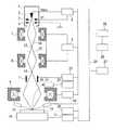
図1は、本発明の走査電子顕微鏡の全体構成を概略的に示す図である。図1において、走査電子顕微鏡は、電子源2、引出電極3及び加速電極4を含む電子銃1から電子ビームを試料ステージ16上の試料15に照射する構成となっている。電子ビームの光路上には、電子ビームを試料ステージ16上の試料15上に集束させるべく、集束レンズ電源6により駆動される第1集束レンズ7及び第2集束レンズ8と、対物レンズ制御電源10により駆動される対物レンズ9とが配置されている。試料ステージ16は、ステージ駆動制御装置17によって駆動される。 FIG. 1 is a diagram schematically showing an overall configuration of a scanning electron microscope of the present invention. In FIG. 1, the scanning electron microscope is configured to irradiate a
この走査電子顕微鏡において、電子源2と引出電極3の間には、電子銃電源5により引出電圧V1が印加されており、この電圧によって電子源2から電子ビーム19が試料ステージ16上に向けて引き出される。アース電位に維持された加速電極4と電子源2との間には、電子銃電源5により加速電圧Vaccが印加されており、電子ビーム19はこの加速電圧Vaccによって加速される。加速された電子ビーム19は、第1集束レンズ7によって、第1集束レンズ7と第2集束レンズ8との間に第1クロスオーバ13が生じるように集束される。また、第1クロスオーバ13と第2集束レンズ8との間に設置された絞り板12によって、電子ビーム19の不要な領域が除去される。さらに、この電子ビーム19は、第2集束レンズ8によって、第2集束レンズ8と対物レンズ9との間に第2クロスオーバ14が生じるように集束される。さらに、この電子ビーム19は、対物レンズ9によって、試料ステージ16上の試料15に集束される。Zセンサ18により検出された試料15の高さ位置に関する情報が対物レンズ9にフィードバックされて、自動焦点合わせが行われる。 In this scanning electron microscope, an extraction voltage V1 is applied between the
電子ビーム19の第2クロスオーバ14と対物レンズ9との間には、電子ビーム走査用偏向器11が配置されている。この電子ビーム走査用偏向器11は、集束された電子ビーム19で試料15を二次元的に走査できるように電子ビーム19を偏向させるためのものである。電子ビーム走査用偏向器11の走査信号は、観察倍率に応じて偏向器制御電源23により制御される。また、試料15には一次電子ビーム19を減速させるリターディング電圧として負の電圧が可変減速電源28によって印加される。リターディング電圧は、可変減速電源28を調整することにより任意に変えることができる。 An electron
集束された電子ビーム19によって試料15が照射され走査されると、試料15から二次電子20が発生する。発生した二次電子20は、検出器21により検出され、信号アンプ22で増幅される。増幅された検出信号は、制御演算部24を通じて描画部25に入力され、描画部25において可視信号に変換されて、試料像表示部26に試料の表面形状の画像として表示される。オペレータは、入力部27を介して上述の各ユニットの制御を行ったり、測定点の指定や寸法測定の指示を行ったりすることができる。 When the
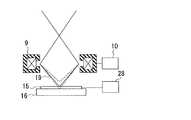
図2は、図1に示す走査電子顕微鏡におけるフォーカス合わせについて説明する図である。前述したとおり、ウェーハ上へのフォーカス条件は、ウェーハに照射される電子19の加速電圧及びウェーハ高さによって決まる。試料15が帯電していなければ、通常、図中の実線で示すように正確に試料15表面上にフォーカスを合わせることができる。しかしながら、試料15が帯電していると、破線で示すようにフォーカス合わせの位置が通常の場合から変動してしまう。フォーカス合わせの位置が試料表面上から変動するとフォーカスが合わず測定点の検出に失敗してしまうことになる。 FIG. 2 is a diagram for explaining focusing in the scanning electron microscope shown in FIG. As described above, the focus condition on the wafer is determined by the acceleration voltage of the
図3は、従来の走査電子顕微鏡及び図1に示す走査電子顕微鏡における試料15周辺の拡大図である。図3(a)に示すように、従来の走査電子顕微鏡では、試料15の上方にリタ−ディング電圧を印加するための電極板29が配置されている。この構成では、電圧が可変減速電源28によって、電極板29と試料15とが同電位となるように制御されている。 FIG. 3 is an enlarged view of the periphery of the
これに対して、図3(b),(c)に示すように、本発明の走査電子顕微鏡では、電極板29の電子ビーム通過口を持つ部分とそれ以外の部分とを分割されており、それぞれ切り替え回路30及び切り替え回路31に接続されていることを特徴とする。図3(b),(c)に示す電極板29の平面図を、それぞれ図4(a),(b)に示す。図4(a),(b)において、電極板29の分割された部分同士は絶縁材料で接続されているものとする。あるいは、電極板29の分割された部分同士は離隔されており別々に保持されていてもよい。 On the other hand, as shown in FIGS. 3B and 3C, in the scanning electron microscope of the present invention, the portion having the electron beam passage opening of the
本発明の走査電子顕微鏡では、図3(b),(c)に示すように、電極板29の電子ビーム通過口を持つ部分とそれ以外の部分とに接続された切り替え回路30及び切り替え回路31を適宜切り替えることにより、両部分の間の静電容量から試料15の帯電電圧を測定することができる。この測定結果により、フォーカス合わせを調整することができる。一方で、試料15の画像を取得する際には、切り替え回路30及び切り替え回路31を、ともに可変減速電源28に接続することにより、電極板29の電子ビーム通過口を持つ部分とそれ以外の部分とを同電位とすればよい。 In the scanning electron microscope of the present invention, as shown in FIGS. 3B and 3C, the switching
こうして正確に測定された試料室内での試料15の帯電電圧の値に基づいて、各光学系を制御することにより、試料15上に正確かつ高速なフォーカス合わせを行うことができることとなる。 By controlling each optical system based on the value of the charging voltage of the
以下に、電極板29の分割された部分同士の静電容量から試料15の帯電量を算出する方法の具体例を示す。
事前準備
(1)Bareウェーハでの静電容量を算出する。 C=Q/V・・・式1
(2)BareウェーハでのC-V直線を算出する。
実測定時
(3)試料の静電容量を測定する。 C’=Q’/V・・・式2
(4)式1,2よりC’を算出する。 C’=C×Q’/Q・・式3
(CとQは(1)より既知でありQ’は Q’=Itより算出)
(5)C→C’による電圧変動を試料帯電電圧とし、(2)の関係式より算出する。A specific example of a method for calculating the charge amount of the
Preparation (1) Calculate the capacitance of the Bare wafer. C = Q / V ... Formula 1
(2) Calculate the CV straight line on the Bare wafer.
During actual measurement (3) The capacitance of the sample is measured. C '= Q' / V ...
(4) C ′ is calculated from
(C and Q are known from (1) and Q 'is calculated from Q' = It)
(5) The voltage fluctuation due to C → C ′ is taken as the sample charging voltage, and calculated from the relational expression (2).
[記号の解説]
Q:Bareウェーハの電荷
Q’:試料の電荷
C:Bareウェーハの静電容量
C’:試料の静電容量
V:電圧
I:電流
t:時間[Explanation of symbols]
Q: Bare wafer charge
Q ': Sample charge
C: Bare wafer capacitance
C ': Sample capacitance
V: Voltage
I: Current
t: time
以上、本発明の走査電子顕微鏡について、具体的な実施の形態を示して説明したが、本発明はこれらに限定されるものではない。当業者であれば、本発明の要旨を逸脱しない範囲内において、上記各実施形態又は他の実施形態にかかる発明の構成及び機能に様々な変更・改良を加えることが可能である。 While the scanning electron microscope of the present invention has been described with reference to specific embodiments, the present invention is not limited to these. A person skilled in the art can make various changes and improvements to the configurations and functions of the invention according to the above-described embodiments or other embodiments without departing from the gist of the present invention.
1…電子銃、2…電子源、3…引出電極、4…加速電極、5…電子銃電源、6…集束レンズ制御電源、7…第1集束レンズ、8…第2集束レンズ、9…対物レンズ、10…対物レンズ制御電源、11…電子ビーム走査用偏向器、12…絞り、13…第1クロスオーバ、14…第2クロスオーバ、15…試料、16…試料ステージ、17…ステージ駆動制御装置、18…Zセンサ、19…電子ビーム、20…二次電子、21…検出器、22…信号アンプ、23…偏向制御電源、24…制御演算装置、25…描画装置、26…試料像表示装置、27…入力装置、28…リターディング電圧、29…電極板、30,31…切り替え回路DESCRIPTION OF SYMBOLS 1 ... Electron gun, 2 ... Electron source, 3 ... Extraction electrode, 4 ... Acceleration electrode, 5 ... Electron gun power supply, 6 ... Focusing lens control power supply, 7 ... 1st focusing lens, 8 ... 2nd focusing lens, 9 ...
Claims (3)
Translated fromJapanese前記電子線源からの電子線を照射する試料を保持するステージと、
前記電子線を前記ステージに保持された試料上に集束させるための対物レンズと、
前記試料と前記対物レンズとの間に配置された電子線の通過開口を有する電極板と、
前記試料と前記電極板との間に電圧を印加して前記電子線源からの電子線を所望の電圧まで減速させるためのリターディング手段と、
を備えた走査電子顕微鏡において、
前記電極板は2以上の互いに絶縁された領域に分割されており、前記電極板の分割された領域のうち前記試料と電気的に接続された1の領域と他の領域との間の静電容量を測定し、その測定値に基づいて前記試料の帯電電圧を検出することを特徴とする走査電子顕微鏡。An electron beam source;
A stage for holding a sample to be irradiated with an electron beam from the electron beam source;
An objective lens for focusing the electron beam on a sample held on the stage;
An electrode plate having an electron beam passage opening disposed between the sample and the objective lens;
Retarding means for applying a voltage between the sample and the electrode plate to decelerate the electron beam from the electron beam source to a desired voltage;
In a scanning electron microscope with
The electrode plate is divided into two or more mutually insulated regions, and among the divided regions of the electrode plate, electrostatic capacitance between one region electrically connected to the sample and another region A scanning electron microscope characterized by measuring a capacitance and detecting a charging voltage of the sample based on the measured value.
検出された前記試料の高さ情報に基づいて、前記リターディング手段及び前記対物レンズを制御して電子線の前記試料に対するフォーカス合わせを行う手段とをさらに備えていることを特徴とする請求項1に記載の走査電子顕微鏡。Means for detecting the height of the sample;
2. The apparatus according to claim 1, further comprising a means for controlling the retarding means and the objective lens based on the detected height information of the sample to focus the electron beam on the sample. A scanning electron microscope according to 1.
Priority Applications (2)
| Application Number | Priority Date | Filing Date | Title |
|---|---|---|---|
| JP2006012744AJP4616180B2 (en) | 2006-01-20 | 2006-01-20 | Scanning electron microscope |
| US11/655,275US7514683B2 (en) | 2006-01-20 | 2007-01-19 | Scanning electron microscope |
Applications Claiming Priority (1)
| Application Number | Priority Date | Filing Date | Title |
|---|---|---|---|
| JP2006012744AJP4616180B2 (en) | 2006-01-20 | 2006-01-20 | Scanning electron microscope |
Publications (2)
| Publication Number | Publication Date |
|---|---|
| JP2007194126Atrue JP2007194126A (en) | 2007-08-02 |
| JP4616180B2 JP4616180B2 (en) | 2011-01-19 |
Family
ID=38449648
Family Applications (1)
| Application Number | Title | Priority Date | Filing Date |
|---|---|---|---|
| JP2006012744AExpired - Fee RelatedJP4616180B2 (en) | 2006-01-20 | 2006-01-20 | Scanning electron microscope |
Country Status (2)
| Country | Link |
|---|---|
| US (1) | US7514683B2 (en) |
| JP (1) | JP4616180B2 (en) |
Cited By (5)
| Publication number | Priority date | Publication date | Assignee | Title |
|---|---|---|---|---|
| JP2009043936A (en)* | 2007-08-09 | 2009-02-26 | Hitachi High-Technologies Corp | electronic microscope |
| WO2011007517A1 (en)* | 2009-07-15 | 2011-01-20 | 株式会社 日立ハイテクノロジーズ | Specimen potential measuring method, and charged particle beam device |
| CN102288628A (en)* | 2011-05-18 | 2011-12-21 | 华南理工大学 | Device with intelligent measurement and control technology for testing secondary electronic emission coefficients of solid material |
| WO2013187115A1 (en)* | 2012-06-15 | 2013-12-19 | 株式会社 日立ハイテクノロジーズ | Charged particle beam device |
| JP2023065369A (en)* | 2018-12-28 | 2023-05-12 | エーエスエムエル ネザーランズ ビー.ブイ. | Systems and methods for focusing charged particle beams |
Families Citing this family (3)
| Publication number | Priority date | Publication date | Assignee | Title |
|---|---|---|---|---|
| JP2013506959A (en)* | 2009-09-30 | 2013-02-28 | カール ツァイス エヌティーエス エルエルシー | Variable energy charged particle system |
| JP6913344B2 (en)* | 2017-03-27 | 2021-08-04 | 株式会社日立ハイテクサイエンス | Charged particle beam device |
| US10096447B1 (en)* | 2017-08-02 | 2018-10-09 | Kla-Tencor Corporation | Electron beam apparatus with high resolutions |
Citations (6)
| Publication number | Priority date | Publication date | Assignee | Title |
|---|---|---|---|---|
| JPS56107166A (en)* | 1981-01-23 | 1981-08-25 | Ando Electric Co Ltd | Surfacial electrometer |
| JPH09178823A (en)* | 1995-12-26 | 1997-07-11 | Dainippon Screen Mfg Co Ltd | Contactless electric measuring sensor |
| JP2000133194A (en)* | 1998-10-29 | 2000-05-12 | Hitachi Ltd | Scanning electron microscope |
| JP2000260371A (en)* | 1999-03-09 | 2000-09-22 | Toshiba Corp | Electrode for electron beam writing apparatus and method of manufacturing the same |
| JP2001052642A (en)* | 1999-08-11 | 2001-02-23 | Toshiba Corp | Scanning electron microscope and fine pattern measurement method |
| JP2005005151A (en)* | 2003-06-12 | 2005-01-06 | Hitachi High-Technologies Corp | Charged particle beam equipment |
Family Cites Families (2)
| Publication number | Priority date | Publication date | Assignee | Title |
|---|---|---|---|---|
| JPH07245075A (en) | 1994-03-04 | 1995-09-19 | Horon:Kk | Automatic focusing device |
| JP3014369B2 (en) | 1998-08-28 | 2000-02-28 | 株式会社日立製作所 | Electron beam device equipped with sample height measuring means |
- 2006
- 2006-01-20JPJP2006012744Apatent/JP4616180B2/ennot_activeExpired - Fee Related
- 2007
- 2007-01-19USUS11/655,275patent/US7514683B2/ennot_activeExpired - Fee Related
Patent Citations (6)
| Publication number | Priority date | Publication date | Assignee | Title |
|---|---|---|---|---|
| JPS56107166A (en)* | 1981-01-23 | 1981-08-25 | Ando Electric Co Ltd | Surfacial electrometer |
| JPH09178823A (en)* | 1995-12-26 | 1997-07-11 | Dainippon Screen Mfg Co Ltd | Contactless electric measuring sensor |
| JP2000133194A (en)* | 1998-10-29 | 2000-05-12 | Hitachi Ltd | Scanning electron microscope |
| JP2000260371A (en)* | 1999-03-09 | 2000-09-22 | Toshiba Corp | Electrode for electron beam writing apparatus and method of manufacturing the same |
| JP2001052642A (en)* | 1999-08-11 | 2001-02-23 | Toshiba Corp | Scanning electron microscope and fine pattern measurement method |
| JP2005005151A (en)* | 2003-06-12 | 2005-01-06 | Hitachi High-Technologies Corp | Charged particle beam equipment |
Cited By (12)
| Publication number | Priority date | Publication date | Assignee | Title |
|---|---|---|---|---|
| JP2009043936A (en)* | 2007-08-09 | 2009-02-26 | Hitachi High-Technologies Corp | electronic microscope |
| WO2011007517A1 (en)* | 2009-07-15 | 2011-01-20 | 株式会社 日立ハイテクノロジーズ | Specimen potential measuring method, and charged particle beam device |
| JP5205515B2 (en)* | 2009-07-15 | 2013-06-05 | 株式会社日立ハイテクノロジーズ | Sample potential measuring method and charged particle beam apparatus |
| US9129775B2 (en) | 2009-07-15 | 2015-09-08 | Hitachi High-Technologies Corporation | Specimen potential measuring method, and charged particle beam device |
| CN102288628A (en)* | 2011-05-18 | 2011-12-21 | 华南理工大学 | Device with intelligent measurement and control technology for testing secondary electronic emission coefficients of solid material |
| WO2013187115A1 (en)* | 2012-06-15 | 2013-12-19 | 株式会社 日立ハイテクノロジーズ | Charged particle beam device |
| JP2014002835A (en)* | 2012-06-15 | 2014-01-09 | Hitachi High-Technologies Corp | Charged particle beam device |
| KR20140143441A (en)* | 2012-06-15 | 2014-12-16 | 가부시키가이샤 히다치 하이테크놀로지즈 | Charged particle beam device |
| US9324540B2 (en) | 2012-06-15 | 2016-04-26 | Hitachi High-Technologies Corporation | Charged particle beam device |
| KR101685274B1 (en)* | 2012-06-15 | 2016-12-09 | 가부시키가이샤 히다치 하이테크놀로지즈 | Charged particle beam device |
| JP2023065369A (en)* | 2018-12-28 | 2023-05-12 | エーエスエムエル ネザーランズ ビー.ブイ. | Systems and methods for focusing charged particle beams |
| KR102863381B1 (en) | 2018-12-28 | 2025-09-24 | 에이에스엠엘 네델란즈 비.브이. | Systems and methods for focusing charged-particle beams |
Also Published As
| Publication number | Publication date |
|---|---|
| JP4616180B2 (en) | 2011-01-19 |
| US20070235646A1 (en) | 2007-10-11 |
| US7514683B2 (en) | 2009-04-07 |
Similar Documents
| Publication | Publication Date | Title |
|---|---|---|
| EP4158674B1 (en) | High throughput multi-beam charged particle inspection system with dynamic control | |
| JP4616180B2 (en) | Scanning electron microscope | |
| JP5103033B2 (en) | Charged particle beam application equipment | |
| TWI592976B (en) | Charged particle beam device and inspection method using the device | |
| US8481935B2 (en) | Scanning electron microscope | |
| US9324540B2 (en) | Charged particle beam device | |
| US20080017797A1 (en) | Pattern inspection and measurement apparatus | |
| JP2009009882A (en) | Charged particle beam application apparatus and sample inspection method | |
| JP4253576B2 (en) | Pattern defect inspection method and inspection apparatus | |
| WO2015050201A1 (en) | Charged particle beam inclination correction method and charged particle beam device | |
| CN117396996A (en) | Multi-beam microscope and method of operating the multi-beam microscope using settings adjusted according to the inspection area | |
| KR102616003B1 (en) | Charged particle beam device, and control method | |
| US8188427B2 (en) | Scanning electron microscope alignment method and scanning electron microscope | |
| JP2001052642A (en) | Scanning electron microscope and fine pattern measurement method | |
| JP2011014299A (en) | Scanning electron microscope | |
| JP6782795B2 (en) | Sample observation method using scanning electron microscope and scanning electron microscope | |
| JP2007012290A (en) | Charged particle beam application equipment | |
| JP4305421B2 (en) | Electron beam adjustment method, charged particle optical system controller, and scanning electron microscope | |
| WO2020115876A1 (en) | Charged particle beam device | |
| JP4484860B2 (en) | Pattern defect inspection method | |
| JP5094612B2 (en) | Sample holding device and charged particle beam device | |
| JP2005338096A (en) | Pattern measuring method and charged particle beam apparatus | |
| JP4238072B2 (en) | Charged particle beam equipment | |
| JP2002352758A (en) | Charged particle beam adjustment method and charged particle beam device | |
| JP5210666B2 (en) | Scanning electron microscope |
Legal Events
| Date | Code | Title | Description |
|---|---|---|---|
| A621 | Written request for application examination | Free format text:JAPANESE INTERMEDIATE CODE: A621 Effective date:20080214 | |
| A977 | Report on retrieval | Free format text:JAPANESE INTERMEDIATE CODE: A971007 Effective date:20100629 | |
| A131 | Notification of reasons for refusal | Free format text:JAPANESE INTERMEDIATE CODE: A131 Effective date:20100706 | |
| A521 | Request for written amendment filed | Free format text:JAPANESE INTERMEDIATE CODE: A523 Effective date:20100906 | |
| TRDD | Decision of grant or rejection written | ||
| A01 | Written decision to grant a patent or to grant a registration (utility model) | Free format text:JAPANESE INTERMEDIATE CODE: A01 Effective date:20101019 | |
| A01 | Written decision to grant a patent or to grant a registration (utility model) | Free format text:JAPANESE INTERMEDIATE CODE: A01 | |
| A61 | First payment of annual fees (during grant procedure) | Free format text:JAPANESE INTERMEDIATE CODE: A61 Effective date:20101021 | |
| R150 | Certificate of patent or registration of utility model | Free format text:JAPANESE INTERMEDIATE CODE: R150 | |
| FPAY | Renewal fee payment (event date is renewal date of database) | Free format text:PAYMENT UNTIL: 20131029 Year of fee payment:3 | |
| LAPS | Cancellation because of no payment of annual fees |