JP2007193469A - TOUCH PANEL, TOUCH INPUT POSITION DETECTING METHOD, ELECTRO-OPTICAL DEVICE, AND ELECTRONIC DEVICE - Google Patents
TOUCH PANEL, TOUCH INPUT POSITION DETECTING METHOD, ELECTRO-OPTICAL DEVICE, AND ELECTRONIC DEVICEDownload PDFInfo
- Publication number
- JP2007193469A JP2007193469AJP2006009469AJP2006009469AJP2007193469AJP 2007193469 AJP2007193469 AJP 2007193469AJP 2006009469 AJP2006009469 AJP 2006009469AJP 2006009469 AJP2006009469 AJP 2006009469AJP 2007193469 AJP2007193469 AJP 2007193469A
- Authority
- JP
- Japan
- Prior art keywords
- touch panel
- surface acoustic
- spacer
- touch
- cover film
- Prior art date
- Legal status (The legal status is an assumption and is not a legal conclusion. Google has not performed a legal analysis and makes no representation as to the accuracy of the status listed.)
- Withdrawn
Links
Images


Classifications
- G—PHYSICS
- G06—COMPUTING OR CALCULATING; COUNTING
- G06F—ELECTRIC DIGITAL DATA PROCESSING
- G06F3/00—Input arrangements for transferring data to be processed into a form capable of being handled by the computer; Output arrangements for transferring data from processing unit to output unit, e.g. interface arrangements
- G06F3/01—Input arrangements or combined input and output arrangements for interaction between user and computer
- G06F3/03—Arrangements for converting the position or the displacement of a member into a coded form
- G06F3/041—Digitisers, e.g. for touch screens or touch pads, characterised by the transducing means
- G06F3/043—Digitisers, e.g. for touch screens or touch pads, characterised by the transducing means using propagating acoustic waves
- G06F3/0436—Digitisers, e.g. for touch screens or touch pads, characterised by the transducing means using propagating acoustic waves in which generating transducers and detecting transducers are attached to a single acoustic waves transmission substrate
- G—PHYSICS
- G02—OPTICS
- G02F—OPTICAL DEVICES OR ARRANGEMENTS FOR THE CONTROL OF LIGHT BY MODIFICATION OF THE OPTICAL PROPERTIES OF THE MEDIA OF THE ELEMENTS INVOLVED THEREIN; NON-LINEAR OPTICS; FREQUENCY-CHANGING OF LIGHT; OPTICAL LOGIC ELEMENTS; OPTICAL ANALOGUE/DIGITAL CONVERTERS
- G02F1/00—Devices or arrangements for the control of the intensity, colour, phase, polarisation or direction of light arriving from an independent light source, e.g. switching, gating or modulating; Non-linear optics
- G02F1/01—Devices or arrangements for the control of the intensity, colour, phase, polarisation or direction of light arriving from an independent light source, e.g. switching, gating or modulating; Non-linear optics for the control of the intensity, phase, polarisation or colour
- G02F1/13—Devices or arrangements for the control of the intensity, colour, phase, polarisation or direction of light arriving from an independent light source, e.g. switching, gating or modulating; Non-linear optics for the control of the intensity, phase, polarisation or colour based on liquid crystals, e.g. single liquid crystal display cells
- G02F1/133—Constructional arrangements; Operation of liquid crystal cells; Circuit arrangements
- G02F1/1333—Constructional arrangements; Manufacturing methods
- G02F1/13338—Input devices, e.g. touch panels
- G—PHYSICS
- G06—COMPUTING OR CALCULATING; COUNTING
- G06F—ELECTRIC DIGITAL DATA PROCESSING
- G06F1/00—Details not covered by groups G06F3/00 - G06F13/00 and G06F21/00
- G06F1/16—Constructional details or arrangements
- G06F1/1613—Constructional details or arrangements for portable computers
- G06F1/1633—Constructional details or arrangements of portable computers not specific to the type of enclosures covered by groups G06F1/1615 - G06F1/1626
- G06F1/1637—Details related to the display arrangement, including those related to the mounting of the display in the housing
- G06F1/1643—Details related to the display arrangement, including those related to the mounting of the display in the housing the display being associated to a digitizer, e.g. laptops that can be used as penpads
- G—PHYSICS
- G06—COMPUTING OR CALCULATING; COUNTING
- G06F—ELECTRIC DIGITAL DATA PROCESSING
- G06F3/00—Input arrangements for transferring data to be processed into a form capable of being handled by the computer; Output arrangements for transferring data from processing unit to output unit, e.g. interface arrangements
- G06F3/01—Input arrangements or combined input and output arrangements for interaction between user and computer
- G06F3/03—Arrangements for converting the position or the displacement of a member into a coded form
- G06F3/033—Pointing devices displaced or positioned by the user, e.g. mice, trackballs, pens or joysticks; Accessories therefor
- G06F3/0354—Pointing devices displaced or positioned by the user, e.g. mice, trackballs, pens or joysticks; Accessories therefor with detection of 2D relative movements between the device, or an operating part thereof, and a plane or surface, e.g. 2D mice, trackballs, pens or pucks
- G06F3/03547—Touch pads, in which fingers can move on a surface
- G—PHYSICS
- G06—COMPUTING OR CALCULATING; COUNTING
- G06F—ELECTRIC DIGITAL DATA PROCESSING
- G06F3/00—Input arrangements for transferring data to be processed into a form capable of being handled by the computer; Output arrangements for transferring data from processing unit to output unit, e.g. interface arrangements
- G06F3/01—Input arrangements or combined input and output arrangements for interaction between user and computer
- G06F3/03—Arrangements for converting the position or the displacement of a member into a coded form
- G06F3/041—Digitisers, e.g. for touch screens or touch pads, characterised by the transducing means
- G06F3/0412—Digitisers structurally integrated in a display
- G—PHYSICS
- G06—COMPUTING OR CALCULATING; COUNTING
- G06F—ELECTRIC DIGITAL DATA PROCESSING
- G06F3/00—Input arrangements for transferring data to be processed into a form capable of being handled by the computer; Output arrangements for transferring data from processing unit to output unit, e.g. interface arrangements
- G06F3/01—Input arrangements or combined input and output arrangements for interaction between user and computer
- G06F3/03—Arrangements for converting the position or the displacement of a member into a coded form
- G06F3/041—Digitisers, e.g. for touch screens or touch pads, characterised by the transducing means
- G06F3/0416—Control or interface arrangements specially adapted for digitisers
- G06F3/04166—Details of scanning methods, e.g. sampling time, grouping of sub areas or time sharing with display driving
Landscapes
- Engineering & Computer Science (AREA)
- Theoretical Computer Science (AREA)
- General Engineering & Computer Science (AREA)
- Physics & Mathematics (AREA)
- General Physics & Mathematics (AREA)
- Human Computer Interaction (AREA)
- Acoustics & Sound (AREA)
- Computer Hardware Design (AREA)
- Nonlinear Science (AREA)
- Crystallography & Structural Chemistry (AREA)
- Optics & Photonics (AREA)
- Chemical & Material Sciences (AREA)
- Mathematical Physics (AREA)
- Position Input By Displaying (AREA)
Abstract
Translated fromJapaneseDescription
Translated fromJapanese本発明は、タッチパネル、そのタッチ入力位置検出方法、電気光学装置および電子機器に関するものである。 The present invention relates to a touch panel, a touch input position detection method thereof, an electro-optical device, and an electronic apparatus.
近年、パーソナルデジタルアシスタント(PDA)、パームトップコンピュータ等の小型情報電子機器の普及に伴い、液晶表示パネル上に入力装置としてタッチパネルを搭載した液晶装置が広く使用されるようになってきている。そのうち、超音波表面弾性波方式のタッチパネルは、ガラス基板の表面上を伝搬する表面弾性波がタッチ入力位置で減衰する性質を利用して、タッチ入力位置を検出するものである。 In recent years, with the spread of small information electronic devices such as personal digital assistants (PDAs) and palmtop computers, liquid crystal devices having a touch panel as an input device on a liquid crystal display panel have been widely used. Among them, the ultrasonic surface acoustic wave type touch panel detects the touch input position by utilizing the property that the surface acoustic wave propagating on the surface of the glass substrate attenuates at the touch input position.
このタッチパネルの一例として、特許文献1に示すように、表面弾性波が伝搬するガラス基板と、表面弾性波を送受信するトランスジューサと、トランスジューサが受信した表面弾性波に基づきタッチ位置を検出する位置検出手段と、ガラス基板に対して空間層を挟んで配置され、ガラス基板の基板対向面に複数のドットスペーサが形成された透明樹脂フィルムとを備えたタッチパネルが提案されている。この透明樹脂フィルムは、物体が接触しないときは基板対向面がガラス基板に接触せず、物体が接触したときは基板対向面がガラス基板に接触するように構成されている。そして、透明樹脂フィルムがガラス基板に接触した位置での表面弾性波の減衰を検知することにより、タッチ入力位置を検出するようになっている。
しかしながら、ガラス基板の表面を伝搬する表面弾性波は、スペーサとの接触によっても減衰する。特許文献1のタッチパネルでは、タッチ入力がない場合でも、透明樹脂フィルムの撓み等により、スペーサとガラス基板とが当接する可能性がある。またスペーサ位置の近傍がタッチ入力位置となった場合には、透明樹脂フィルムより先にスペーサがガラス基板と当接する可能性がある。これらの場合には、スペーサ位置をタッチ入力位置として誤検出するという問題がある。 However, the surface acoustic wave propagating on the surface of the glass substrate is also attenuated by contact with the spacer. In the touch panel of
本発明は、上記課題を解決するためになされたものであって、タッチ入力位置の誤検出を防止することが可能なタッチパネル、およびそのタッチ入力位置検出方法の提供を目的とする。また、信頼性に優れた電気光学装置および電子機器の提供を目的とする。 The present invention has been made to solve the above-described problems, and an object of the present invention is to provide a touch panel capable of preventing erroneous detection of a touch input position, and a touch input position detection method thereof. It is another object of the present invention to provide an electro-optical device and electronic equipment with excellent reliability.
上記目的を達成するため、本発明に係るタッチパネルは、タッチ入力面を備えたタッチパネル基板と、前記タッチパネル基板の前記入力面に対向して離間配置されたカバーフィルムと、前記タッチパネル基板から前記カバーフィルムに向けて立設されたスペーサと、前記タッチパネル基板の前記入力面に表面弾性波を伝搬させる送信子と、前記入力面を伝搬した前記表面弾性波を測定する受信子と、前記カバーフィルムを押圧しない状態での前記表面弾性波の測定値を基準値として格納するメモリと、タッチパネル使用中における前記表面弾性波の測定値と前記基準値との差分が有意となる位置を、タッチ入力位置として検出する判断部と、を備えることを特徴とする。 In order to achieve the above object, a touch panel according to the present invention includes a touch panel substrate having a touch input surface, a cover film spaced apart from the input surface of the touch panel substrate, and the cover film from the touch panel substrate. A spacer erected toward the surface, a transmitter for propagating surface acoustic waves to the input surface of the touch panel substrate, a receiver for measuring the surface acoustic waves propagated through the input surface, and pressing the cover film A memory that stores the measured value of the surface acoustic wave in a non-operating state as a reference value, and a position where a difference between the measured value of the surface acoustic wave and the reference value during use of the touch panel is significant is detected as a touch input position And a determination unit.
この構成によれば、タッチパネル基板上にスペーサが立設されているので、スペーサによる減衰を折り込んで表面弾性波の基準値を測定することができる。これにより、タッチパネル使用中における前記表面弾性波の測定値と前記基準値との差分は、スペーサ位置において有意にならない。したがって、スペーサ位置をタッチ入力位置と判断する誤検出を防止することができる。しかも、カバーフィルムは可撓性を有するので、スペーサ位置の近傍がタッチ入力位置となっても、スペーサを強く押圧することがない。そのため、カバーフィルムを押圧しない状態で表面弾性波の基準値を測定すれば足りることになり、タッチパネルの使用準備(キャリブレーション)作業を簡素化することができる。 According to this configuration, since the spacer is erected on the touch panel substrate, it is possible to measure the reference value of the surface acoustic wave by folding the attenuation by the spacer. Thereby, the difference between the measured value of the surface acoustic wave and the reference value during use of the touch panel is not significant at the spacer position. Therefore, it is possible to prevent erroneous detection in which the spacer position is determined as the touch input position. Moreover, since the cover film has flexibility, even if the vicinity of the spacer position becomes the touch input position, the spacer is not strongly pressed. Therefore, it is sufficient to measure the reference value of the surface acoustic wave without pressing the cover film, and the touch panel use preparation (calibration) operation can be simplified.
一方、本発明に係るタッチパネルのタッチ入力位置検出方法は、タッチ入力面を備えたタッチパネル基板と、前記タッチパネル基板の前記入力面に対向して離間配置されたカバーフィルムと、前記タッチパネル基板から前記カバーフィルムに向けて立設されたスペーサと、前記タッチパネル基板の前記入力面に表面弾性波を伝搬させる送信子と、前記入力面を伝搬した前記表面弾性波を測定する受信子と、を備えたタッチパネルのタッチ入力位置検出方法であって、前記カバーフィルムを押圧しない状態での前記表面弾性波の測定値を基準値として記録する工程と、タッチパネル使用中における前記表面弾性波の測定値と前記基準値との差分が有意となる位置をタッチ入力位置として検出する工程と、を有することを特徴とする。
この構成によれば、スペーサ位置をタッチ入力位置と判断する誤検出を防止することができる。Meanwhile, a touch input position detection method for a touch panel according to the present invention includes a touch panel substrate having a touch input surface, a cover film spaced apart from the input surface of the touch panel substrate, and the cover from the touch panel substrate. A touch panel comprising: a spacer erected toward the film; a transmitter that propagates surface acoustic waves to the input surface of the touch panel substrate; and a receiver that measures the surface acoustic waves propagated through the input surface. The touch input position detection method, the step of recording the surface acoustic wave measurement value without pressing the cover film as a reference value, and the surface acoustic wave measurement value and the reference value during use of the touch panel And a step of detecting, as a touch input position, a position where the difference between and becomes significant.
According to this configuration, it is possible to prevent erroneous detection in which the spacer position is determined as the touch input position.
一方、本発明に係る電気光学装置は、複数の画素が整列配置された画像表示装置と、前記画像表示装置の画像表示側に配置された前記タッチパネルと、を有することを特徴とする。
この構成によれば、タッチ入力位置の誤検出を防止することが可能なタッチパネルを供えているので、信頼性に優れた電気光学装置を提供することができる。On the other hand, an electro-optical device according to the present invention includes an image display device in which a plurality of pixels are arranged and the touch panel disposed on the image display side of the image display device.
According to this configuration, since the touch panel capable of preventing erroneous detection of the touch input position is provided, an electro-optical device with excellent reliability can be provided.
また、前記画像表示装置が、前記タッチパネル基板として機能することが望ましい。
この構成によれば、電気光学装置を薄型化することができる。しかも、タッチパネルのスペーサを画像表示装置に位置合わせして配置することができるので、画像表示装置における複数の画素の境界領域にタッチパネルのスペーサを精度よく配置することができる。Moreover, it is desirable that the image display device functions as the touch panel substrate.
According to this configuration, the electro-optical device can be thinned. In addition, since the spacers of the touch panel can be aligned with the image display device, the spacers of the touch panel can be accurately arranged in the boundary areas of the plurality of pixels in the image display device.
また前記画像表示装置は、液晶を挟持する一対の基板と、前記一対の基板の外側に配置された一対の偏光板とを備えた液晶装置であり、前記一対の偏光板のうち画像表示側の前記偏光板が、前記カバーフィルムとして機能することが望ましい。
この構成によれば、電気光学装置を薄型化することができる。Further, the image display device is a liquid crystal device including a pair of substrates sandwiching a liquid crystal and a pair of polarizing plates arranged outside the pair of substrates, and the image display side of the pair of polarizing plates It is desirable that the polarizing plate functions as the cover film.
According to this configuration, the electro-optical device can be thinned.
また前記タッチパネルにおける前記スペーサは、平面視において前記画像表示装置における前記複数の画素の境界領域に配置されていることが望ましい。
この構成によれば、タッチパネルのスペーサに起因する画像表示装置の開口率の低下を抑制することができる。Moreover, it is desirable that the spacer in the touch panel is disposed in a boundary region of the plurality of pixels in the image display device in a plan view.
According to this structure, the fall of the aperture ratio of the image display apparatus resulting from the spacer of a touch panel can be suppressed.
一方、本発明に係る電子機器は、上述した電気光学装置を備えたことを特徴とする。
この構成によれば、タッチ入力位置の誤検出を防止することが可能なタッチパネルを供えているので、信頼性に優れた電子機器を提供することができる。On the other hand, an electronic apparatus according to the present invention includes the above-described electro-optical device.
According to this configuration, since the touch panel capable of preventing erroneous detection of the touch input position is provided, it is possible to provide an electronic device with excellent reliability.
以下、本発明の実施形態につき、図面を参照して説明する。なお、以下の説明に用いる各図面では、各部材を認識可能な大きさとするため、各部材の縮尺を適宜変更している。なお本明細書では、液晶装置の各構成部材における液晶層側を内側と呼び、その反対側を外側と呼ぶことにする。また本明細書では、タッチパネルの各構成部材におけるタッチ入力側を表側と呼び、その反対側を裏側と呼ぶことにする。 Embodiments of the present invention will be described below with reference to the drawings. In each drawing used for the following description, the scale of each member is appropriately changed to make each member a recognizable size. In the present specification, the liquid crystal layer side of each component of the liquid crystal device is referred to as an inner side, and the opposite side is referred to as an outer side. Moreover, in this specification, the touch input side in each component of the touch panel is referred to as a front side, and the opposite side is referred to as a back side.
(第1実施形態)
図1は第1実施形態に係る電気光学装置の説明図であり、図2のA−A線に相当する部分における断面図である。図1に示すように、第1実施形態に係る電気光学装置100は、画像表示装置である液晶装置1の画像表示側(表側)に、タッチパネル50を配置したものである。(First embodiment)
FIG. 1 is an explanatory diagram of the electro-optical device according to the first embodiment, and is a cross-sectional view taken along a line AA in FIG. As shown in FIG. 1, the electro-
(液晶装置)
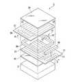
図2は、液晶装置の分解斜視図である。なお本実施形態ではパッシブマトリクス型の液晶装置を例にして説明するが、本発明をアクティブマトリクス型の液晶装置に適用することも可能である。(Liquid crystal device)
FIG. 2 is an exploded perspective view of the liquid crystal device. Note that although a passive matrix liquid crystal device is described as an example in this embodiment, the present invention can also be applied to an active matrix liquid crystal device.
液晶装置1では、ガラス等の透明材料からなる一対の下部基板10および上部基板20が対向配置されている。両基板10,20の間にはスペーサ(図示せず)が配置され、両基板10,20の間隔が例えば5μm程度に保持されている。また両基板10,20は、熱硬化型や紫外線硬化型などの接着剤からなるシール材30によって、周縁部が接合されている。そのシール材30の一部には、両基板10,20から外側に突出した液晶注入口32が設けられている。その液晶注入口32から、両基板10,20とシール材30とによって囲まれた空間に、STN(Super Twisted Nematic)液晶などの液晶材料が封入されている。その液晶が注入された後に、液晶注入口32が封止材31によって封止されている。 In the
下部基板10の内面には、ITO等の透明導電材料からなるコモン電極12がストライプ状に形成されている。また上部基板20の内面には、ITO等の透明導電材料からなるセグメント電極22がストライプ状に形成されている。なおセグメント電極22およびコモン電極12は直交するように配置され、その交点付近が液晶装置の画素となっている。 On the inner surface of the
一方、下部基板10の外側には入射側偏光板18が配置され、上部基板20の外側には出射側偏光板28が配置されている。なお入射側偏光板18および出射側偏光板28は、それぞれの透過軸が所定角度(例えば約90°)で交差するように配置されている。また、入射側偏光板18の外側には、バックライト2が配置されている。 On the other hand, an incident
一方、下部基板10が上部基板20の側方に張り出し形成され、その張り出し部11にコモン電極12が延長形成されている。また張り出し部11の先端には、液晶装置1と他の基板とを接続するための配線パターン13が形成されている。そして、配線パターン13とコモン電極12との間には、他の基板からの信号に基づいてコモン電極12を駆動するための駆動用IC38が実装されている。同様に、上部基板20にも張り出し部21が形成され、その張り出し部21にセグメント電極22が延長形成されて、セグメント電極22を駆動するための駆動用IC39が実装されている。 On the other hand, the
図1に戻り、下部基板の内面には、複数の画素4に対応して、カラーフィルタを構成する赤(R)、緑(G)および青(B)の色材層16R、16G、16Bが形成されている。なお、各色材層16R、16G、16Bの間には遮光膜15が形成され、隣接する画素4からの光洩れが防止されている。また、各色材層16R、16G、16Bおよび遮光膜15の表面には平坦化膜(保護膜)17が形成され、その平坦化膜17の表面にコモン電極12が形成されている。そのコモン電極12の表面には、電界無印加時における液晶の配向状態を規制する配向膜14が形成されている。 Returning to FIG. 1, on the inner surface of the lower substrate, red (R), green (G), and blue (B)
一方、上部基板20の内面にはセグメント電極22が形成されている。そのセグメント電極22の表面には、電圧無印加時における液晶の配向状態を規制する配向膜24が形成されている。なお、上部基板20の配向膜24による液晶の配向方向と、下部基板10の配向膜14による液晶の配向方向とが、所定角度(例えば約90°)で交差するように各配向膜14,24が形成されている。 On the other hand, a
そして、バックライト2からの光が入射側偏光板18に入射すると、入射側偏光板18の透過軸に沿った直線偏光のみが入射側偏光板18を透過する。入射側偏光板18を透過した直線偏光は、両基板10,20に挟持された液晶層35を透過する過程で、電界無印加時における液晶の配向状態にしたがって旋光する。液晶層35を透過した直線偏光のうち、出射側偏光板28の透過軸と一致する成分のみが、出射側偏光板28を透過する。 When the light from the
また、コモン電極12またはセグメント電極22のいずれか一方にデータ信号が供給され他方に走査信号が供給されると、両電極12,22の交点の画素4に配置された液晶層35に電圧が印加される。その電圧レベルに応じて液晶分子の配向状態が変化し、液晶層35に入射した直線偏光の旋光角度が調整される。これにより、液晶装置1の画素4ごとに光透過率が制御され、画像表示が行われるようになっている。 Further, when a data signal is supplied to one of the
(タッチパネルの断面構成)
次に、タッチパネル50について説明する。タッチパネル50は、ガラス等の透明材料からなるタッチパネル基板41と、そのタッチパネル基板41のタッチ入力面41aに対向して離間配置されたカバーフィルム42とを備えている。カバーフィルム42は、ポリエチレンテレフタレート(PET)やポリカーボネート(PC)、アクリル、三酢酸セルロース(TAC)等の透明材料により、可撓性を有するフィルム状に形成されている。なおカバーフィルム42の表面には、ARコーティング等の反射防止処理が施されていてもよい。(Cross-sectional configuration of touch panel)
Next, the
タッチパネル基板41とカバーフィルム42との間の周縁部には、シール材44が配置されている。これにより、タッチパネル基板41とカバーフィルム42との間に、空気や不活性ガス等からなるガス層45が形成されている。なおガス層45の厚さは数μm程度に形成されているが、その厚さを10μm以上に厚くすればニュートンリングの発生を防止することができる。 A sealing
なお後述するように、タッチパネル基板41のタッチ入力面41aには表面弾性波が伝搬する。そして、カバーフィルム42を介してタッチパネル基板41のタッチ入力面41aを押圧することにより、表面弾性波を減衰させてタッチ入力位置を検出することができるようになっている。 As described later, a surface acoustic wave propagates to the
このように、タッチパネル基板41に対向してカバーフィルム42を配置することにより、タッチ入力面41aの表面に異物が付着するのを防止することが可能になり、タッチ入力位置の誤検出を防止することができる。また、ガラス基板に比べてカバーフィルムは弾性率が低いので、タッチパネル基板41との当接により表面弾性波を確実に吸収して減衰させることができる。さらにタッチパネル基板41が破壊した場合でも、カバーフィルム42によって破片の飛散を防止することがでる。 In this manner, by disposing the
一方、タッチパネル基板41とカバーフィルム42との間には、スペーサ43が設けられている。スペーサ43は、樹脂材料等により柱状に形成され、タッチパネル基板41のタッチ入力面41a上に立設されている。このスペーサ43を形成するには、まずタッチパネル基板41のタッチ入力面41a上に感光性樹脂材料の被膜を形成し、次にフォトリソグラフィを用いてパターニングすればよい。また液滴吐出法により樹脂材料の液状体を所定位置に吐出し、硬化させてもよい。 On the other hand, a
スペーサ43は、高さ数μm程度に形成されている。なおスペーサ43の高さをガス層45の厚さより小さく形成して、スペーサ43の先端とカバーフィルム42との間に隙間を形成してもよく、スペーサ43の高さをガス層45の厚さと同等に形成して、スペーサ43の先端をカバーフィルム42の裏面に当接させてもよい。 The
このようにスペーサ43を形成することにより、タッチパネル基板41とカバーフィルム42との望まれない接触を防止することが可能になり、タッチ入力有無およびタッチ入力位置の誤検出を防止することができる。またスペーサ43を形成することにより、タッチパネル基板41とカバーフィルム42との距離を略一定に保持することが可能になり、ニュートンリングの発生を防止することができる。 By forming the
タッチパネル基板41上には、複数のスペーサ43が数mm程度の間隔で配置されている。なお平面視(タッチパネル基板の法線方向から見た場合)において、液晶装置1における複数の画素4の境界領域に、スペーサ43を配置することが望ましい。すなわち、液晶装置1における遮光膜15の形成領域(非開口部)にスペーサ43を配置する。これにより、スペーサ43に起因する液晶装置1の開口率の低下を抑制することができる。 A plurality of
(タッチパネルの平面構成)
図3は、タッチパネル基板の平面図である。タッチパネル50は、タッチパネル基板41のタッチ入力面41a上の中心部に入力対応面59を有し、その入力対応面59上に複数のスペーサ43が設置されている。タッチ入力面41a上の隅には、X軸方向に破線矢印で示す表面弾性波Wvxを発生させるX送信子51と、Y軸方向に破線矢印で示す表面弾性波Wvyを発生させるY送信子54とが設置されている。これらの送信子51,54は、図示しない圧電振動子より発生したバルク波を、X軸方向やY軸方向といった特定の方向の表面波に変換することにより、表面弾性波Wvx、Wvyを発生させるものである。また、タッチ入力面41a上の別の隅には、X送信子51によって発生した表面弾性波Wvxを検出するX受信子52と、Y送信子54によって発生した表面弾性波Wvyを検出するY受信子53とが設置されている。(Plane configuration of touch panel)
FIG. 3 is a plan view of the touch panel substrate. The
X送信子51、Y送信子54、X受信子52、Y受信子53は、制御部60に電気的に接続されている。制御部60は、X送信子51およびY送信子54に駆動信号を送信することにより、X送信子51およびY送信子54に表面弾性波Wvx、Wvyを発生させる。また制御部60には、X受信子52およびY受信子53が受信した表面弾性波Wvx、Wvyの受信信号が入力される。 The
X送信子51によって発生された表面弾性波Wvxは、X軸方向に伝搬し、反射配列55に入射する。反射配列55は、反射エレメント55aの配列である。反射エレメントは、表面弾性波の伝搬する方向を、その表面弾性波を反射することにより変える役割を有する。反射配列55における各反射エレメント55aは、X軸に対しおよそ45度の角度で配列されており、表面弾性波Wvxの方向を−Y軸方向へ向ける。−Y軸方向へ向けられた表面弾性波Wvxは、そのまま入力対応面59を通過し、反射配列57へ入射する。反射配列57における各反射エレメント57aは、X軸に対しおよそ−45度の角度で配列されており、表面弾性波Wvxを−X軸方向へ向ける役割を有する。反射エレメント57aによって−X軸方向へ向けられた表面弾性波Wvxは、X受信子52によって検出される。 The surface acoustic wave Wvx generated by the
一方、Y送信子54によって発生された表面弾性波Wvyは、Y軸方向に伝搬し、反射配列56へ入射する。反射配列56における各反射エレメント56aは、Y軸に対しおよそ45度の角度で配列されており、表面弾性波Wvyの方向を−X軸方向へ向ける。−X軸方向へ向けられた表面弾性波Wvyは、そのまま入力対応面59を通過し、反射配列58へ入射する。反射配列58における各反射エレメント58aは、Y軸に対しおよそ−45度の角度で配列されており、表面弾性波Wvyの方向を−Y軸方向へ向ける。−Y軸方向へ向けられた表面弾性波Wvyは、Y受信子53によって検出される。 On the other hand, the surface acoustic wave Wvy generated by the
図4(b)は、検出された表面弾性波の包絡線波形の一例を示すグラフである。図4(b)において、横軸は時間を示し、縦軸は表面弾性波の信号強度を示している。ここでは、図3に示すX送信子51より表面弾性波Wvxがタッチパネル基板41の表面上に発信された場合を考えてみる。X送信子51より発生した表面弾性波Wvxは、反射配列55、57を経由して、X受信子52に検出される。このとき、反射配列55、57における各反射エレメントは、異なる長さの複数の経路のセットを定め、反射配列55、57における連続する各反射エレメントが反射する表面弾性波Wvxは、次第に長くなる経路を通って、X受信子52に到達する。そのため、図4(b)に示すように、X受信子によって検出された受信信号の波形は、発信信号と比較して、時間に対して間延びした台形状の波形となる。 FIG. 4B is a graph showing an example of the envelope waveform of the detected surface acoustic wave. In FIG. 4B, the horizontal axis indicates time, and the vertical axis indicates the signal intensity of the surface acoustic wave. Here, let us consider a case where the surface acoustic wave Wvx is transmitted from the
図4(a)は、タッチパネルのタッチ入力状態の断面図である。ユーザが指やペンなどでカバーフィルム42をタッチすると、タッチ入力位置におけるカバーフィルム42がたわみ、タッチパネル基板41のタッチ入力面に接触する。タッチパネル基板41上を伝搬する表面弾性波は、カバーフィルム42が接触した位置を通過する際、カバーフィルム42により吸収されて減衰する。 FIG. 4A is a cross-sectional view of the touch input state of the touch panel. When the user touches the
そのため、図4(b)に示す表面弾性波Wvxの包絡線波形には、タッチによる信号の欠落が発生する。受信信号を検出してから、このタッチによる信号の欠落が発生するまでの時間Tgを計測することにより、タッチ入力位置のX座標を特定することができる。なおタッチ入力位置のY座標を特定する場合においても同様である。このように、図3に示す制御部60は、X受信子52により検出された表面弾性波Wvxと、Y受信子53により検出された表面弾性波Wvyとを基に、タッチ入力位置のX座標およびY座標を算出するようになっている。 Therefore, in the envelope waveform of the surface acoustic wave Wvx shown in FIG. 4B, a signal loss due to touch occurs. The X coordinate of the touch input position can be specified by measuring the time Tg from when the received signal is detected until the signal is lost due to the touch. The same applies when specifying the Y coordinate of the touch input position. As described above, the
図5は、制御部のブロック図である。制御部60は、XY送信子に駆動信号を出力する送信部と、XY受信子から受信信号が入力される受信部とを備えている。その受信信号は、増幅器により増幅され、検波器によって検波されて、A/D変換器により量子化される。タッチパネル使用中における表面弾性波の受信信号は、量子化された後に、測定値として第1RAM62に格納される。 FIG. 5 is a block diagram of the control unit. The
ところで、タッチパネル基板上を伝搬する表面弾性波は、上記のようにカバーフィルムが接触した位置を通過する際に減衰するが、図6(a)に示すスペーサ43の位置を通過する際にも減衰する。そのためスペーサ43の位置においても、図6(b)に示す受信信号の欠落が発生する。そこで、スペーサ位置における受信信号の欠落を把握するため、タッチパネルの使用準備(キャリブレーション)作業として、カバーフィルムを押圧しない状態で表面弾性波の受信信号を測定しておく。その受信信号は、量子化された後に、基準値として図5に示す第2RAM63に格納される。 By the way, the surface acoustic wave propagating on the touch panel substrate attenuates when passing through the position where the cover film contacts as described above, but also attenuates when passing through the position of the
また図5に示す制御部60は、ROM61、判断部64および通信手段を備えている。ROM61には、タッチ入力有無を判断する閾値が格納されている。また判断部64は、第1RAM62に格納された測定値と、第2RAM63に格納された基準値との差分をとる。その差分が、ROM61に格納された閾値を超えた部分を、タッチ入力位置として検出するものである。また通信手段は、検出されたタッチ入力位置のXY座標を出力するものである。 The
(タッチパネルのタッチ入力位置検出方法)
次に、タッチパネルのタッチ入力位置検出方法について説明する。
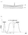
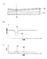
図7はスペーサ位置の近傍がタッチ入力位置となる場合であり、図7(a)は断面図であり、図7(b)は基準値および測定値の信号強度のグラフであり、図7(c)は測定値と基準値との差分のグラフである。(Touch input position detection method for touch panel)
Next, a touch input position detection method for the touch panel will be described.
7 shows the case where the vicinity of the spacer position is the touch input position, FIG. 7A is a cross-sectional view, FIG. 7B is a graph of the signal strength of the reference value and the measured value, and FIG. c) is a graph of the difference between the measured value and the reference value.
最初に、タッチパネルの使用準備(キャリブレーション)作業として、カバーフィルムを押圧しない状態で表面弾性波の受信信号を測定する。まず、タッチパネル基板上に表面弾性波を送信し、スペーサの位置において減衰した表面弾性波を受信して、制御部に入力する。これにより、図7(b)に示すように、スペーサ位置における信号強度が低下した基準値91が生成される。この基準値91を、図5に示す第2RAM63に格納する。 First, as a touch panel use preparation (calibration) operation, a surface acoustic wave reception signal is measured without pressing the cover film. First, a surface acoustic wave is transmitted onto the touch panel substrate, and the surface acoustic wave attenuated at the position of the spacer is received and input to the control unit. Thereby, as shown in FIG. 7B, a
次に、タッチパネル使用中にタッチ入力位置の検出を行う。まず、図7(a)に示すタッチパネル基板41上に表面弾性波を送信する。その表面弾性波は、スペーサ43の位置に加えて、カバーフィルム42がタッチパネル基板41に接触した位置(タッチ入力位置)において減衰する。その表面弾性波を受信して、制御部に入力する。これにより、図7(b)に示すように、スペーサ位置およびタッチ入力位置における信号強度が低下した測定値92が生成される。この測定値92を、図5に示す第1RAM62に格納する。 Next, the touch input position is detected while using the touch panel. First, a surface acoustic wave is transmitted onto the
次に、制御部60における判断部64は、第2RAM63から基準値を読み出し、第1RAM62から測定値を読み出して、図7(c)に示す両者の差分97を算出する。タッチ入力位置では、基準値91には受信強度の低下がなく、測定値92の受信強度のみが低下しているので、差分97が有意となっている。これに対してスペーサ位置では、基準値91および測定値92のいずれも受信強度が同等に低下しているので、差分97はほとんど0になっている。 Next, the
次に判断部は、図7(c)に示す差分97と、予め登録された閾値96とを比較する。そして、差分97が閾値96を超えた場合に、その位置をタッチ入力位置として検出する。なお閾値96として、基準値または測定値に重畳するノイズレベルより大きな値を設定しておけば、タッチ入力位置の誤検出を低減することができる。 Next, the determination unit compares the
このように本実施形態では、タッチパネル基板上にスペーサが立設されているので、スペーサによる減衰を折り込んで表面弾性波の基準値を測定することができる。これにより、タッチパネル使用中における前記表面弾性波の測定値と前記基準値との差分は、スペーサ位置において有意にならず、スペーサ位置をタッチ入力位置と判断する誤検出を防止することができる。 As described above, in this embodiment, since the spacer is erected on the touch panel substrate, the reference value of the surface acoustic wave can be measured by folding the attenuation by the spacer. As a result, the difference between the measured value of the surface acoustic wave and the reference value during use of the touch panel is not significant at the spacer position, and erroneous detection that determines the spacer position as the touch input position can be prevented.
ところで、従来のタッチパネルでは、タッチパネル基板に対向して、弾性率の高いガラス基板が配置されていた。このガラス基板を押圧すると、図7(a)に示すように、タッチ入力位置の近傍に配置されたスペーサ43を、同時に強く押圧することになる。これにより、図7(b)に示す従来の測定値93は、スペーサ位置での信号強度の低下量が、基準値91に比べて大きくなる。そのため、図7(c)に示す従来の差分98は、押圧位置に加えてスペーサ位置でも有意になる。これにより、タッチ入力位置の誤検出が多発するという問題がある。 By the way, in the conventional touch panel, the glass substrate with a high elastic modulus was arrange | positioned facing the touch panel substrate. When this glass substrate is pressed, as shown in FIG. 7A, the
なお、ガラス基板を押圧した状態で図7(b)に示す基準値91を測定すれば、スペーサ位置での信号強度の低下量が従来の測定値93と同等になる。しかしながら、タッチパネル使用中と同様にガラス基板を押圧することは不可能であり、またタッチパネルの使用準備(キャリブレーション)作業が煩雑になる。 If the
これに対して、本実施形態のタッチパネルでは、タッチパネル基板に対向して、弾性率の低いカバーフィルムが配置されている。カバーフィルムは可撓性を有するので、スペーサ位置の近傍がタッチ入力位置となっても、スペーサを強く押圧することがない。そのため、カバーフィルムを押圧しない状態で表面弾性波の基準値を測定すれば足りることになり、タッチパネルの使用準備(キャリブレーション)作業を簡素化することができる。 On the other hand, in the touch panel of the present embodiment, a cover film having a low elastic modulus is disposed facing the touch panel substrate. Since the cover film has flexibility, even if the vicinity of the spacer position becomes the touch input position, the spacer is not strongly pressed. Therefore, it is sufficient to measure the reference value of the surface acoustic wave without pressing the cover film, and the touch panel use preparation (calibration) operation can be simplified.
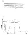
図8はスペーサ位置がタッチ入力位置となる場合であり、図8(a)は断面図であり、図8(b)は基準値および測定値の信号強度のグラフであり、図8(c)は測定値と基準値との差分のグラフである。
図8(a)に示すように、スペーサ43の位置においてカバーフィルム42を押圧した場合について検討する。この場合、図8(b)に示す測定値92は、スペーサ位置での信号強度の低下量が、基準値91に比べて大きくなる。そのため、図8(c)に示す差分97は、スペーサ位置において有意となり、閾値96を超える。これにより、スペーサ位置をタッチ入力位置として検出することができる。FIG. 8 shows the case where the spacer position is the touch input position, FIG. 8A is a cross-sectional view, FIG. 8B is a graph of the signal intensity of the reference value and the measured value, and FIG. Is a graph of the difference between the measured value and the reference value.
As shown in FIG. 8A, the case where the
ところで、従来のタッチ入力位置検出方法では、タッチパネル使用前のキャリブレーションによってスペーサ位置を検出しておき、スペーサ位置をタッチ入力位置の検出対象から除外していた。すなわち、タッチパネル使用中にスペーサ位置が押圧されても、その位置をタッチ入力位置として検出することができなかった。これに対して、本実施形態のタッチ入力位置検出方法では、上述したようにスペーサ位置をタッチ入力位置として検出することができる。これにより、タッチ入力位置の検出精度を向上させることができる。 By the way, in the conventional touch input position detection method, the spacer position is detected by calibration before using the touch panel, and the spacer position is excluded from the touch input position detection target. That is, even if the spacer position is pressed during use of the touch panel, the position cannot be detected as the touch input position. On the other hand, in the touch input position detection method of this embodiment, the spacer position can be detected as the touch input position as described above. Thereby, the detection accuracy of a touch input position can be improved.
(第2実施形態)
図9は、第2実施形態に係る電気光学装置の説明図であり、図2のA−A線に相当する部分における断面図である。図9に示す第2実施形態に係る電気光学装置は、第1実施形態のカバーフィルムに代えて、液晶装置1の画像表示側の偏光板28を配置したものである。なお第1実施形態と同様の構成となる部分については、その詳細な説明を省略する。(Second Embodiment)
FIG. 9 is an explanatory diagram of the electro-optical device according to the second embodiment, and is a cross-sectional view taken along a line AA in FIG. In the electro-optical device according to the second embodiment shown in FIG. 9, a
第2実施形態では、液晶装置1の上部基板20の外側に、タッチパネル50のタッチパネル基板41が装着されている。そのタッチパネル基板41のタッチ入力面41aに対向して、液晶装置1の偏光板28が配置されている。この偏光板28は、ポリビニルアルコール(PVA)等にヨウ素をドープした偏光フィルムを、三酢酸セルロース(TAC)等からなるベース基板に装着したものである。したがって、偏光板28の弾性率は、第1実施形態のカバーフィルムの弾性率と同等になっている。 In the second embodiment, the
このように、第1実施形態のカバーフィルムに代えて偏光板28を配置した場合でも、第1実施形態と同様の効果を奏することができる。しかも、第2実施形態ではカバーフィルムが削減されるので、電気光学装置を薄型化することができる。これに対して第1実施形態では、偏光板としての機能にとらわれず、カバーフィルムの材料を適宜選択することができる。 Thus, even if it replaces with the cover film of 1st Embodiment and the
(第3実施形態)
図10は、第3実施形態に係る電気光学装置の説明図であり、図2のA−A線に相当する部分における断面図である。図10に示す第3実施形態に係る電気光学装置は、液晶装置の上部基板20が、タッチパネル基板として機能するものである。なお、第1実施形態および第2実施形態と同様の構成となる部分については、その詳細な説明を省略する。(Third embodiment)
FIG. 10 is an explanatory diagram of the electro-optical device according to the third embodiment, and is a cross-sectional view taken along a line AA in FIG. In the electro-optical device according to the third embodiment shown in FIG. 10, the
第3実施形態では、液晶装置1の上部基板20の表面に、表面弾性波の送信子、反射配列および受信子(いずれも不図示)が設けられている。また上部基板20の表面に、スペーサ43が設けられている。そして第2実施形態と同様に、上部基板20に対向して偏光板28が配置されている。このように、液晶装置1の上部基板20をタッチパネル基板として機能させる構成としたので、電気光学装置を薄型化することができる。 In the third embodiment, a surface acoustic wave transmitter, a reflective array, and a receiver (all not shown) are provided on the surface of the
なお上述したスペーサ43は、液晶装置1における複数の画素4の境界領域に配置されている。第1実施形態において、スペーサを所定領域に配置するには、タッチパネル基板に位置合わせしてスペーサを形成し、液晶装置に位置合わせしてタッチパネルを装着する必要がある。これに対して、第3実施形態では、液晶装置1に位置合わせしてスペーサを形成すればよい。したがって、スペーサを精度よく所定領域に配置することが可能になり、スペーサに起因する液晶装置の開口率の低下を抑制することができる。 The
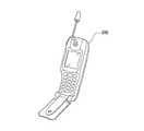
(電子機器)
次に、実施形態の電気光学装置を備えた電子機器の例について、図11を用いて説明する。図11は、携帯電話の斜視図である。上述した電気光学装置は、携帯電話300の液晶表示部を構成している。(Electronics)
Next, an example of an electronic apparatus including the electro-optical device according to the embodiment will be described with reference to FIG. FIG. 11 is a perspective view of a mobile phone. The electro-optical device described above constitutes the liquid crystal display unit of the
なお、上述した電気光学装置は、携帯電話以外にも種々の電子機器に適用することができる。例えば、液晶プロジェクタ、マルチメディア対応のパーソナルコンピュータ(PC)およびエンジニアリング・ワークステーション(EWS)、ページャ、ワードプロセッサ、テレビ、ビューファインダ型またはモニタ直視型のビデオテープレコーダ、電子手帳、電子卓上計算機、カーナビゲーション装置、POS端末、タッチパネルを備えた装置などの電子機器に適用することが可能である。いずれの場合でも、タッチ入力位置の誤検出を防止することが可能なタッチパネルを備えているので、信頼性の高い電子機器を提供することができる。 Note that the above-described electro-optical device can be applied to various electronic devices other than mobile phones. For example, LCD projectors, multimedia-compatible personal computers (PCs) and engineering workstations (EWS), pagers, word processors, TVs, viewfinder type or monitor direct view type video tape recorders, electronic notebooks, electronic desk calculators, car navigation systems The present invention can be applied to electronic devices such as a device, a POS terminal, and a device provided with a touch panel. In any case, since the touch panel capable of preventing erroneous detection of the touch input position is provided, a highly reliable electronic device can be provided.
なお、本発明の技術範囲は、上述した実施形態に限定されるものではなく、本発明の趣旨を逸脱しない範囲において、上述した実施形態に種々の変更を加えたものを含む。すなわち、実施形態で挙げた具体的な材料や構成などはほんの一例に過ぎず、適宜変更が可能である。 It should be noted that the technical scope of the present invention is not limited to the above-described embodiments, and includes those in which various modifications are made to the above-described embodiments without departing from the spirit of the present invention. That is, the specific materials and configurations described in the embodiments are merely examples, and can be changed as appropriate.
例えば、上記実施形態ではパッシブマトリクス方式の液晶装置を例にして説明したが、スイッチング素子として薄膜トランジスタ(Thin Film Transistor;TFT)や薄膜ダイオード(Thin Film Diode;TFD)等を用いたアクティブマトリクス方式の液晶装置に本発明を適用することも可能である。また、上記実施形態では透過型の液晶装置を例にして説明したが、反射型や半透過反射型の液晶装置に本発明を適用することも可能である。 For example, in the above-described embodiment, a passive matrix liquid crystal device has been described as an example. However, an active matrix liquid crystal using a thin film transistor (TFT), a thin film diode (TFD), or the like as a switching element. The present invention can also be applied to an apparatus. Further, although the transmissive liquid crystal device has been described as an example in the above embodiment, the present invention can also be applied to a reflective or transflective liquid crystal device.
また画像表示装置として、上記実施形態では液晶装置を採用したが、液晶装置のように電界により物質の屈折率が変化して光の透過率を変化させる電気光学効果を有する装置の他、電気エネルギーを光学エネルギーに変換する装置等を採用することも可能である。すなわち本発明は、液晶装置だけでなく、有機EL(Electro-Luminescence)装置や無機EL装置、プラズマディスプレイ装置、電気泳動ディスプレイ装置、電子放出素子を用いた表示装置(Field Emission Display 及び Surface-Conduction Electron-Emitter Display 等)などの発光装置等に対しても、広く適用することが可能である。 As the image display device, the liquid crystal device is used in the above embodiment. However, the liquid crystal device has an electro-optical effect in which the refractive index of the substance is changed by an electric field to change the light transmittance, as well as the electric energy. It is also possible to employ a device or the like that converts the light into optical energy. That is, the present invention is not limited to a liquid crystal device, but an organic EL (Electro-Luminescence) device, an inorganic EL device, a plasma display device, an electrophoretic display device, and a display device using an electron-emitting device (Field Emission Display and Surface-Conduction Electron). -Emitter Display etc.) can also be widely applied.
Wvx,Wvy…表面弾性波 1…液晶装置(画像表示装置) 4…画素 10…下部基板 18…偏光板 20…上部基板 28…偏光板 35…液晶 41…タッチパネル基板 41a…タッチ入力面 42…カバーフィルム 43…スペーサ 50…タッチパネル 51…X送信子 52…X受信子 53…Y受信子 54…Y送信子 60…制御部 63…第2RAM 64…判断部 91…基準値 92…測定値 97…差分 Wvx, Wvy ... surface
Claims (7)
Translated fromJapanese前記タッチパネル基板の前記入力面に対向して離間配置されたカバーフィルムと、
前記タッチパネル基板から前記カバーフィルムに向けて立設されたスペーサと、
前記タッチパネル基板の前記入力面に表面弾性波を伝搬させる送信子と、前記入力面を伝搬した前記表面弾性波を測定する受信子と、
前記カバーフィルムを押圧しない状態での前記表面弾性波の測定値を基準値として格納するメモリと、
タッチパネル使用中における前記表面弾性波の測定値と前記基準値との差分が有意となる位置を、タッチ入力位置として検出する判断部と、
を備えることを特徴とするタッチパネル。A touch panel substrate with a touch input surface;
A cover film spaced apart from the input surface of the touch panel substrate;
A spacer erected from the touch panel substrate toward the cover film;
A transmitter for propagating surface acoustic waves to the input surface of the touch panel substrate; a receiver for measuring the surface acoustic waves propagated through the input surface;
A memory for storing a measurement value of the surface acoustic wave in a state where the cover film is not pressed as a reference value;
A determination unit that detects, as a touch input position, a position where a difference between the measured value of the surface acoustic wave during use of the touch panel and the reference value is significant;
A touch panel comprising:
前記タッチパネル基板の前記入力面に対向して離間配置されたカバーフィルムと、
前記タッチパネル基板から前記カバーフィルムに向けて立設されたスペーサと、
前記タッチパネル基板の前記入力面に表面弾性波を伝搬させる送信子と、前記入力面を伝搬した前記表面弾性波を測定する受信子と、を備えたタッチパネルのタッチ入力位置検出方法であって、
前記カバーフィルムを押圧しない状態での前記表面弾性波の測定値を基準値として記録する工程と、
タッチパネル使用中における前記表面弾性波の測定値と前記基準値との差分が有意となる位置をタッチ入力位置として検出する工程と、
を有することを特徴とするタッチパネルのタッチ入力位置検出方法。A touch panel substrate with a touch input surface;
A cover film spaced apart from the input surface of the touch panel substrate;
A spacer erected from the touch panel substrate toward the cover film;
A touch input position detection method for a touch panel, comprising: a transmitter that propagates surface acoustic waves to the input surface of the touch panel substrate; and a receiver that measures the surface acoustic waves propagated through the input surface,
Recording the surface acoustic wave measurement value without pressing the cover film as a reference value;
Detecting a position at which a difference between the measured value of the surface acoustic wave and the reference value during use of the touch panel is significant as a touch input position;
A touch input position detection method for a touch panel, comprising:
前記画像表示装置の画像表示側に配置された請求項1に記載のタッチパネルと、
を有することを特徴とする電気光学装置。An image display device in which a plurality of pixels are arranged and arranged;
The touch panel according to claim 1 disposed on the image display side of the image display device,
An electro-optical device comprising:
前記一対の偏光板のうち画像表示側の前記偏光板が、前記カバーフィルムとして機能することを特徴とする請求項3または請求項4に記載の電気光学装置。The image display device is a liquid crystal device including a pair of substrates that sandwich a liquid crystal, and a pair of polarizing plates disposed outside the pair of substrates,
The electro-optical device according to claim 3, wherein the polarizing plate on the image display side of the pair of polarizing plates functions as the cover film.
Priority Applications (6)
| Application Number | Priority Date | Filing Date | Title |
|---|---|---|---|
| JP2006009469AJP2007193469A (en) | 2006-01-18 | 2006-01-18 | TOUCH PANEL, TOUCH INPUT POSITION DETECTING METHOD, ELECTRO-OPTICAL DEVICE, AND ELECTRONIC DEVICE |
| EP06027002AEP1818790A2 (en) | 2006-01-18 | 2006-12-28 | Touch panel, method for detecting touch input position, electro-optic device, and electronic device |
| KR1020070004373AKR100831487B1 (en) | 2006-01-18 | 2007-01-15 | Touch panel, method for detecting touch input position, electro-optic device, and electronic device |
| TW096101636ATW200805126A (en) | 2006-01-18 | 2007-01-16 | Touch panel, method for detecting touch input position, electro-optic device, and electronic device |
| CNA2007100017267ACN101004655A (en) | 2006-01-18 | 2007-01-16 | Touch panel, method for detecting touch input position, electro-optic device, and electronic device |
| US11/654,307US20070165009A1 (en) | 2006-01-18 | 2007-01-17 | Touch panel, method for detecting touch input position, electro-optic device, and electronic device |
Applications Claiming Priority (1)
| Application Number | Priority Date | Filing Date | Title |
|---|---|---|---|
| JP2006009469AJP2007193469A (en) | 2006-01-18 | 2006-01-18 | TOUCH PANEL, TOUCH INPUT POSITION DETECTING METHOD, ELECTRO-OPTICAL DEVICE, AND ELECTRONIC DEVICE |
Publications (1)
| Publication Number | Publication Date |
|---|---|
| JP2007193469Atrue JP2007193469A (en) | 2007-08-02 |
Family
ID=37814281
Family Applications (1)
| Application Number | Title | Priority Date | Filing Date |
|---|---|---|---|
| JP2006009469AWithdrawnJP2007193469A (en) | 2006-01-18 | 2006-01-18 | TOUCH PANEL, TOUCH INPUT POSITION DETECTING METHOD, ELECTRO-OPTICAL DEVICE, AND ELECTRONIC DEVICE |
Country Status (6)
| Country | Link |
|---|---|
| US (1) | US20070165009A1 (en) |
| EP (1) | EP1818790A2 (en) |
| JP (1) | JP2007193469A (en) |
| KR (1) | KR100831487B1 (en) |
| CN (1) | CN101004655A (en) |
| TW (1) | TW200805126A (en) |
Cited By (4)
| Publication number | Priority date | Publication date | Assignee | Title |
|---|---|---|---|---|
| JP2010232162A (en)* | 2009-03-27 | 2010-10-14 | Lg Display Co Ltd | Organic electroluminescence display |
| JP2016091203A (en)* | 2014-10-31 | 2016-05-23 | 日本電信電話株式会社 | Shield for touch screen, electronic device |
| JP2016201120A (en)* | 2014-09-02 | 2016-12-01 | エヴォ インターナショナル リミテッド | Glass touch screen protector |
| JP2021128766A (en)* | 2020-02-12 | 2021-09-02 | アイト ベスローテンヴェンノーツハップAito BV | Piezoelectric sensing device |
Families Citing this family (44)
| Publication number | Priority date | Publication date | Assignee | Title |
|---|---|---|---|---|
| JP2008040608A (en)* | 2006-08-02 | 2008-02-21 | Fujitsu Component Ltd | Surface acoustic wave system touch panel |
| JP4650699B2 (en)* | 2008-03-06 | 2011-03-16 | Necインフロンティア株式会社 | Input device, input method, and program |
| US8508495B2 (en) | 2008-07-03 | 2013-08-13 | Apple Inc. | Display with dual-function capacitive elements |
| JP5055231B2 (en)* | 2008-09-08 | 2012-10-24 | 株式会社ジャパンディスプレイイースト | Touch position detection method for touch panel |
| KR100930497B1 (en)* | 2008-11-14 | 2009-12-09 | 이성호 | Touch panel |
| US8217913B2 (en)* | 2009-02-02 | 2012-07-10 | Apple Inc. | Integrated touch screen |
| TWI570494B (en)* | 2009-04-17 | 2017-02-11 | 元太科技工業股份有限公司 | Touch electrophoretic display |
| TW201113787A (en)* | 2009-10-05 | 2011-04-16 | Au Optronics Corp | Touch display panel and display device |
| TWI422905B (en)* | 2009-10-28 | 2014-01-11 | Wintek Corp | Touch panel integrated in display |
| US8624878B2 (en)* | 2010-01-20 | 2014-01-07 | Apple Inc. | Piezo-based acoustic and capacitive detection |
| CN101901085A (en)* | 2010-07-07 | 2010-12-01 | 深圳创维-Rgb电子有限公司 | A Method of Improving the Stability of Infrared Touch System |
| TW201224899A (en)* | 2010-12-14 | 2012-06-16 | xiang-yu Li | Synchronization device for detecting induced electric field as capacitive touch position detection |
| US10198097B2 (en) | 2011-04-26 | 2019-02-05 | Sentons Inc. | Detecting touch input force |
| US9189109B2 (en) | 2012-07-18 | 2015-11-17 | Sentons Inc. | Detection of type of object used to provide a touch contact input |
| US9639213B2 (en) | 2011-04-26 | 2017-05-02 | Sentons Inc. | Using multiple signals to detect touch input |
| US9477350B2 (en) | 2011-04-26 | 2016-10-25 | Sentons Inc. | Method and apparatus for active ultrasonic touch devices |
| US11327599B2 (en) | 2011-04-26 | 2022-05-10 | Sentons Inc. | Identifying a contact type |
| TWI457681B (en)* | 2011-09-30 | 2014-10-21 | E Ink Holdings Inc | Electronic paper display |
| EP2780783B1 (en) | 2011-11-18 | 2022-12-28 | Sentons Inc. | Detecting touch input force |
| US10235004B1 (en)* | 2011-11-18 | 2019-03-19 | Sentons Inc. | Touch input detector with an integrated antenna |
| US11262253B2 (en) | 2017-08-14 | 2022-03-01 | Sentons Inc. | Touch input detection using a piezoresistive sensor |
| CN104169847B (en) | 2011-11-18 | 2019-03-12 | 森顿斯公司 | local haptic feedback |
| US9348468B2 (en) | 2013-06-07 | 2016-05-24 | Sentons Inc. | Detecting multi-touch inputs |
| KR101976067B1 (en)* | 2012-07-25 | 2019-05-09 | 삼성디스플레이 주식회사 | A display device providing touch emitting key unit |
| CN103576995A (en)* | 2012-07-31 | 2014-02-12 | 电子触控产品解决方案公司 | Touch sensitive display with acoustic isolation |
| TWI461896B (en)* | 2012-11-07 | 2014-11-21 | Chih Chung Lin | Photoelectric conversion touch panel |
| US10088936B2 (en)* | 2013-01-07 | 2018-10-02 | Novasentis, Inc. | Thin profile user interface device and method providing localized haptic response |
| US9336723B2 (en) | 2013-02-13 | 2016-05-10 | Apple Inc. | In-cell touch for LED |
| JP6266892B2 (en)* | 2013-04-01 | 2018-01-24 | シナプティクス・ジャパン合同会社 | Driver IC and display device |
| JP5567727B1 (en)* | 2013-09-17 | 2014-08-06 | 株式会社フジクラ | Electronic device and control method of electronic device |
| US9459715B1 (en) | 2013-09-20 | 2016-10-04 | Sentons Inc. | Using spectral control in detecting touch input |
| US9880671B2 (en)* | 2013-10-08 | 2018-01-30 | Sentons Inc. | Damping vibrational wave reflections |
| CN116560524B (en) | 2013-12-13 | 2024-10-01 | 苹果公司 | Integrated touch and display architecture for self-capacitance touch sensor |
| US10133382B2 (en) | 2014-05-16 | 2018-11-20 | Apple Inc. | Structure for integrated touch screen |
| US10048811B2 (en) | 2015-09-18 | 2018-08-14 | Sentons Inc. | Detecting touch input provided by signal transmitting stylus |
| JP6386484B2 (en) | 2016-01-19 | 2018-09-05 | ファナック株式会社 | Electrical device with foreign object detection panel |
| CN106293219B (en)* | 2016-08-03 | 2019-09-06 | 京东方科技集团股份有限公司 | A device with pressure touch function and its control method |
| US10908741B2 (en) | 2016-11-10 | 2021-02-02 | Sentons Inc. | Touch input detection along device sidewall |
| US10296144B2 (en) | 2016-12-12 | 2019-05-21 | Sentons Inc. | Touch input detection with shared receivers |
| US10126877B1 (en) | 2017-02-01 | 2018-11-13 | Sentons Inc. | Update of reference data for touch input detection |
| US10585522B2 (en) | 2017-02-27 | 2020-03-10 | Sentons Inc. | Detection of non-touch inputs using a signature |
| US11157115B2 (en)* | 2017-03-31 | 2021-10-26 | Apple Inc. | Composite cover material for sensitivity improvement of ultrasonic touch screens |
| US11580829B2 (en) | 2017-08-14 | 2023-02-14 | Sentons Inc. | Dynamic feedback for haptics |
| JP6908493B2 (en)* | 2017-10-11 | 2021-07-28 | ローム株式会社 | Touch panel control circuit, control method, touch-type input device using it, electronic device |
Family Cites Families (9)
| Publication number | Priority date | Publication date | Assignee | Title |
|---|---|---|---|---|
| DE69416960T2 (en)* | 1993-12-07 | 1999-08-19 | Seiko Epson Corp | Touch panel input device and method for generating input signals for an information processing device |
| JPH09203890A (en)* | 1996-01-25 | 1997-08-05 | Sharp Corp | LIQUID CRYSTAL DISPLAY DEVICE WITH INPUT FUNCTION, REFLECTION TYPE LIQUID CRYSTAL DISPLAY DEVICE WITH INPUT FUNCTION, AND METHODS OF MANUFACTURING THE SAME |
| KR20000009756A (en) | 1998-07-28 | 2000-02-15 | 윤종용 | Image display element |
| KR100356989B1 (en) | 1999-04-13 | 2002-10-18 | 주식회사 엘지씨아이 | Polarizer unified transparent conductive film, touch panel unified polarizer and flat panel display unified touch panel |
| US6366277B1 (en)* | 1999-10-13 | 2002-04-02 | Elo Touchsystems, Inc. | Contaminant processing system for an acoustic touchscreen |
| US6975305B2 (en)* | 2001-12-07 | 2005-12-13 | Nec Infrontia Corporation | Pressure-sensitive touch panel |
| JP2003280821A (en)* | 2002-03-26 | 2003-10-02 | Matsushita Electric Ind Co Ltd | Light transmissive touch panel |
| JP4093308B2 (en)* | 2002-11-01 | 2008-06-04 | 富士通株式会社 | Touch panel device and contact position detection method |
| JP4198527B2 (en)* | 2003-05-26 | 2008-12-17 | 富士通コンポーネント株式会社 | Touch panel and display device |
- 2006
- 2006-01-18JPJP2006009469Apatent/JP2007193469A/ennot_activeWithdrawn
- 2006-12-28EPEP06027002Apatent/EP1818790A2/ennot_activeWithdrawn
- 2007
- 2007-01-15KRKR1020070004373Apatent/KR100831487B1/ennot_activeExpired - Fee Related
- 2007-01-16CNCNA2007100017267Apatent/CN101004655A/enactivePending
- 2007-01-16TWTW096101636Apatent/TW200805126A/enunknown
- 2007-01-17USUS11/654,307patent/US20070165009A1/ennot_activeAbandoned
Cited By (5)
| Publication number | Priority date | Publication date | Assignee | Title |
|---|---|---|---|---|
| JP2010232162A (en)* | 2009-03-27 | 2010-10-14 | Lg Display Co Ltd | Organic electroluminescence display |
| JP2016201120A (en)* | 2014-09-02 | 2016-12-01 | エヴォ インターナショナル リミテッド | Glass touch screen protector |
| JP2016091203A (en)* | 2014-10-31 | 2016-05-23 | 日本電信電話株式会社 | Shield for touch screen, electronic device |
| JP2021128766A (en)* | 2020-02-12 | 2021-09-02 | アイト ベスローテンヴェンノーツハップAito BV | Piezoelectric sensing device |
| JP7702256B2 (en) | 2020-02-12 | 2025-07-03 | アイト ベスローテンヴェンノーツハップ | Piezoelectric Sensing Device |
Also Published As
| Publication number | Publication date |
|---|---|
| TW200805126A (en) | 2008-01-16 |
| EP1818790A2 (en) | 2007-08-15 |
| CN101004655A (en) | 2007-07-25 |
| US20070165009A1 (en) | 2007-07-19 |
| KR100831487B1 (en) | 2008-05-22 |
| KR20070076488A (en) | 2007-07-24 |
Similar Documents
| Publication | Publication Date | Title |
|---|---|---|
| JP2007193469A (en) | TOUCH PANEL, TOUCH INPUT POSITION DETECTING METHOD, ELECTRO-OPTICAL DEVICE, AND ELECTRONIC DEVICE | |
| US7593067B2 (en) | Electro-optical device and electronic equipment having touch panel with resin having particular elastic modulus | |
| JP4412289B2 (en) | Electro-optical device and electronic apparatus | |
| JP4506742B2 (en) | Touch panel, electro-optical device and electronic apparatus | |
| US8077162B2 (en) | Touch panel and display device | |
| US10175826B2 (en) | Touch device and display device including the same | |
| JP2008083491A (en) | Electro-optical device and electronic equipment | |
| JP2018036506A (en) | Display device | |
| CN101008880A (en) | Touch panel, electrooptical device, and electronic apparatus | |
| JP2007200230A (en) | Touch panel, electro-optical device and electronic equipment | |
| JP2009003672A (en) | Touch panel device, electro-optical device, and electronic device | |
| JP2007264688A (en) | Touch panel, electro-optic device, and electronic appliance | |
| JP2006243428A (en) | Display device, display device manufacturing method, liquid crystal display device, liquid crystal display device manufacturing method, and electronic apparatus | |
| JP2009075297A (en) | Liquid crystal display and electronic device | |
| JP2007264686A (en) | Touch panel, electrooptical device and electronic equipment | |
| JP4613858B2 (en) | Touch panel, electro-optical device and electronic apparatus | |
| JP2006343918A (en) | Electro-optical device, touch panel, and touch panel control method | |
| JP2006343919A (en) | Electro-optical device and touch panel | |
| JP2007264687A (en) | Touch panel, electrooptic device and electronic equipment |
Legal Events
| Date | Code | Title | Description |
|---|---|---|---|
| A977 | Report on retrieval | Free format text:JAPANESE INTERMEDIATE CODE: A971007 Effective date:20090206 | |
| A131 | Notification of reasons for refusal | Free format text:JAPANESE INTERMEDIATE CODE: A131 Effective date:20090210 | |
| A761 | Written withdrawal of application | Free format text:JAPANESE INTERMEDIATE CODE: A761 Effective date:20090409 |