JP2007184840A - Solid-state imaging device and electronic camera using the same - Google Patents
Solid-state imaging device and electronic camera using the sameDownload PDFInfo
- Publication number
- JP2007184840A JP2007184840AJP2006002640AJP2006002640AJP2007184840AJP 2007184840 AJP2007184840 AJP 2007184840AJP 2006002640 AJP2006002640 AJP 2006002640AJP 2006002640 AJP2006002640 AJP 2006002640AJP 2007184840 AJP2007184840 AJP 2007184840A
- Authority
- JP
- Japan
- Prior art keywords
- focus detection
- photoelectric conversion
- unit
- conversion unit
- solid
- Prior art date
- Legal status (The legal status is an assumption and is not a legal conclusion. Google has not performed a legal analysis and makes no representation as to the accuracy of the status listed.)
- Granted
Links
Images


Landscapes
- Focusing (AREA)
- Automatic Focus Adjustment (AREA)
- Transforming Light Signals Into Electric Signals (AREA)
Abstract
Translated fromJapaneseDescription
Translated fromJapanese本発明は、焦点検出が可能な固体撮像素子及びこれを用いた電子カメラに関する。 The present invention relates to a solid-state imaging device capable of focus detection and an electronic camera using the same.
近年、CCD(Charge Coupld Device)型やCMOS(Complementary Metal Oxide Semiconductor)型(或いは増幅型と呼ばれる)などの固体撮像素子を用いたビデオカメラや電子カメラが広く普及している。固体撮像素子は複数の単位画素が二次元アレイ状に配置され、単位画素は受ける光を電気信号に変換する光電変換部や光電変換部の電気信号を読み取るための信号線などで構成される。また、光電変換部の光が入射する側にマイクロレンズがオンチップで形成される。 In recent years, video cameras and electronic cameras using a solid-state image sensor such as a CCD (Charge Coupled Device) type or a CMOS (Complementary Metal Oxide Semiconductor) type (or called an amplification type) have become widespread. A solid-state imaging device includes a plurality of unit pixels arranged in a two-dimensional array, and each unit pixel includes a photoelectric conversion unit that converts received light into an electric signal, a signal line for reading an electric signal of the photoelectric conversion unit, and the like. A microlens is formed on-chip on the light incident side of the photoelectric conversion unit.
一方、一般的なカメラは、自動的にカメラレンズの焦点を合わせるAF(Auto Focus)機能を有しており、焦点検出するための専用の焦点検出素子が使用されるが、専用素子を設けると、カメラのコスト低減や小型化の障害となるため、固体撮像素子で焦点検出を行う瞳分割位相差方式などが提案されている。
例えば、特許文献1,2および3において、二つの光電変換部をペアとして焦点位置を検出する瞳分割位相差方式に関する技術が開示されている。特許文献1および2は、画像用の信号と焦点検出用の信号との出力方法に関する技術で、特許文献3は、焦点検出の際に二つの画素がペアになるように、光学要素アレイを固体撮像素子の前面に挿入する技術である。
For example, Patent Documents 1, 2, and 3 disclose a technique related to a pupil division phase difference method for detecting a focal position with two photoelectric conversion units as a pair. Patent Documents 1 and 2 are techniques related to an output method of an image signal and a focus detection signal. Patent Document 3 is a solid-state optical element array so that two pixels are paired during focus detection. This is a technique for inserting the image sensor in front of it.
一般に撮像エリアの周辺部の単位画素においては、マイクロレンズにより集光された光が撮像エリアの外周方向にシフトし、そのシフト量は、主に撮像エリア中心から外周方向への距離とマイクロレンズから光電変換部までの距離とに比例する。また、その固体撮像素子をカメラに使用した場合のカメラレンズの射出瞳距離に反比例する。
ところが、上記の特許文献1,2および3に記載されているような従来の技術では、撮像エリアの周辺部の単位画素において、マイクロレンズが適切に配置されていないため、撮像エリアの中心部から周辺部に行くに従って、マイクロレンズにより集光された光が、光電変換部に適切に集光されなくなる。画像用光電変換部だけでなく、同様に焦点検出用光電変換部においても、光が適切に集光されず、いわゆる、光のけられが生じる。その結果、焦点検出用光電変換部の感度が低下し、カメラのAF精度が劣化する。In general, in the unit pixel at the periphery of the imaging area, the light collected by the microlens shifts in the outer circumferential direction of the imaging area, and the amount of shift is mainly from the distance from the center of the imaging area to the outer circumferential direction and the microlens. It is proportional to the distance to the photoelectric conversion unit. Further, it is inversely proportional to the exit pupil distance of the camera lens when the solid-state imaging device is used in a camera.
However, in the conventional techniques as described in Patent Documents 1, 2, and 3 described above, since the microlenses are not properly arranged in the unit pixels in the peripheral part of the imaging area, As it goes to the periphery, the light collected by the microlens is not properly collected by the photoelectric conversion unit. Not only the image photoelectric conversion unit but also the focus detection photoelectric conversion unit does not collect light properly, and so-called light scatter occurs. As a result, the sensitivity of the focus detection photoelectric conversion unit decreases, and the AF accuracy of the camera deteriorates.
また、一つの単位画素に一対の焦点検出用光電変換部を有する単位画素においては、単位画素の受光部の開口位置を限定することにより、撮影する画像の瞳分割画像を取得することが可能となり、同一画像において、瞳分割画像の出力差の量に応じてデフォーカス量を算出することができる。特に撮像エリア周辺部の単位画素においては、瞳分割を行うための一対の焦点検出用光電変換部の開口位置を限定することにより、瞳分割した光を検出することができる。ペアとなる一対の瞳分割光は、それぞれがペアとなる一対の焦点検出用光電変換部に入射されなければならないが、焦点検出用光電変換部の開口部の限定する方向が適切でない場合は、瞳分割光がけられて、焦点検出用光電変換部に入射されなかったり、隣の焦点検出用光電変換部に入射されてしまうなど、AF精度が劣化してしまう。 In addition, in a unit pixel having a pair of focus detection photoelectric conversion units in one unit pixel, it is possible to acquire a pupil-divided image of an image to be captured by limiting the opening position of the light receiving unit of the unit pixel. In the same image, the defocus amount can be calculated according to the output difference amount of the pupil divided image. In particular, in the unit pixels in the periphery of the imaging area, the pupil-divided light can be detected by limiting the opening positions of the pair of focus detection photoelectric conversion units for pupil division. The pair of pupil-divided lights that make a pair must be incident on the pair of focus-detecting photoelectric conversion units, respectively, but if the direction limited by the opening of the focus-detecting photoelectric conversion unit is not appropriate, The AF accuracy is deteriorated, for example, when the pupil-divided light is scattered and does not enter the focus detection photoelectric conversion unit or enters the adjacent focus detection photoelectric conversion unit.
図13は、撮像エリアの周辺部分において、一対の焦点検出用光電変換部を有する単位画素の焦点検出用光電変換部の開口部分の形状と瞳分割光との関係を示した図である。
図13(a)と(c)は、カメラレンズの射出瞳距離が大きい場合の瞳分割像の位置を示し、図13(b)と(d)は、カメラレンズの射出瞳距離が小さい場合の瞳分割像の位置をそれぞれ示しており、瞳分割像の変位方向および変位量は同じである。ところが、図13(b)と(d)との瞳分割像の受光状態は明らかに異なる。つまり、図13(b)において、単位画素801上の瞳分割像804および805は、理想的な位置806および807から上方(撮像エリアの周辺部)に向かってずれているが、瞳分割像804および805の一部は焦点検出用光電変換部802および803のそれぞれに入射されている。これに対して、図13(d)では、瞳分割像810および811は、理想的な位置812および813から上方に向かってずれているため、瞳分割像811は本来入射すべき焦点検出用光電変換部809ではなく、他方の焦点検出用光電変換部808に入射され、瞳分割像810は完全にけられて、検出できなくなっている。FIG. 13 is a diagram illustrating the relationship between the shape of the opening of the focus detection photoelectric conversion unit of the unit pixel having the pair of focus detection photoelectric conversion units and the pupil-divided light in the peripheral portion of the imaging area.
FIGS. 13A and 13C show the position of the pupil split image when the exit pupil distance of the camera lens is large, and FIGS. 13B and 13D show the case where the exit pupil distance of the camera lens is small. The positions of the pupil divided images are respectively shown, and the displacement direction and the displacement amount of the pupil divided images are the same. However, the light receiving states of the pupil division images in FIGS. 13B and 13D are clearly different. That is, in FIG. 13B, the
このように、従来技術では、焦点検出用光電変換部の配置が良くない場合に、撮像エリア周辺部の単位画素で、瞳分割像がけられてしまうため、正確な焦点検出ができないという課題があった。
上記に鑑み、本発明の目的は、撮像エリアの周辺部においても、カメラレンズの射出瞳距離等の撮像条件に影響を受けることなく、AF精度を劣化させずに、位相差焦点検出が可能な固体撮像素子及びこれを用いた電子カメラを提供することである。As described above, in the related art, when the focus detection photoelectric conversion unit is not well arranged, a pupil division image is generated at the unit pixel in the periphery of the imaging area, and thus there is a problem that accurate focus detection cannot be performed. It was.
In view of the above, an object of the present invention is to detect a phase difference focus even in a peripheral portion of an imaging area without being affected by imaging conditions such as an exit pupil distance of a camera lens and without deteriorating AF accuracy. A solid-state imaging device and an electronic camera using the same are provided.
請求項1に係る発明の固体撮像素子は、撮像エリアにマトリクス状に配置され、画像用光電変換部を有する単位画素と、前記単位画素の中に少なくとも一つの焦点検出用光電変換部を有し、一つまたは二つの単位画素で瞳分割の1単位を構成し、且つ、前記撮像エリアの中心を軸とする同心円の略接線方向が瞳分割方向になるように前記焦点検出用光電変換部が配置された焦点検出単位とを有する。 A solid-state imaging device according to a first aspect of the present invention includes unit pixels that are arranged in a matrix in an imaging area and have an image photoelectric conversion unit, and at least one focus detection photoelectric conversion unit in the unit pixel. The focus detection photoelectric conversion unit forms one unit of pupil division with one or two unit pixels, and the substantially tangential direction of a concentric circle with the center of the imaging area as an axis is the pupil division direction. And a focus detection unit arranged.
請求項2に係る発明は、請求項1に記載の固体撮像素子において、連続する複数の前記焦点検出単位からなる焦点検出ブロックを構成し、前記焦点検出用ブロックの中心に位置する前記焦点検出単位の前記焦点検出用光電変換部が、前記撮像エリアの中心を軸とする同心円の略接線方向が瞳分割方向になるように配置され、前記焦点検出用ブロックの中心以外に位置する前記焦点検出単位の前記焦点検出用光電変換部が、前記焦点検出用ブロックの中心に位置する前記焦点検出単位の前記焦点検出用光電変換部と同じ位置に配置されたことを特徴とする。 According to a second aspect of the present invention, in the solid-state imaging device according to the first aspect, the focus detection unit includes a focus detection block including a plurality of continuous focus detection units and is located at the center of the focus detection block. The focus detection unit is arranged such that a substantially tangential direction of a concentric circle with the center of the imaging area as an axis is a pupil division direction, and the focus detection photoelectric conversion unit is located at a position other than the center of the focus detection block The focus detection photoelectric conversion unit is arranged at the same position as the focus detection photoelectric conversion unit of the focus detection unit positioned at the center of the focus detection block.
請求項3に係る発明は、請求項2に記載の固体撮像素子において、前記焦点検出ブロックは、連続する複数の前記焦点検出単位が直線状に配置されたことを特徴とする。
請求項4に係る発明は、請求項2に記載の固体撮像素子において、前記焦点検出ブロックは、連続する複数の前記焦点検出単位が前記撮像エリアの中心を軸とする略同心円状に配置されたことを特徴とする。According to a third aspect of the present invention, in the solid-state imaging device according to the second aspect, the focus detection block includes a plurality of continuous focus detection units arranged linearly.
According to a fourth aspect of the present invention, in the solid-state imaging device according to the second aspect, the focus detection block includes a plurality of continuous focus detection units arranged in a substantially concentric shape with the center of the imaging area as an axis. It is characterized by that.
請求項5に係る発明は、請求項1乃至4のいずれか一項に記載の固体撮像素子において、前記単位画素にマイクロレンズを設け、前記焦点検出単位の前記マイクロレンズが、前記撮像エリアの中心を軸とする略同心円状に配置されたことを特徴とする。
請求項6に係る発明は、請求項5に記載の固体撮像素子において、前記固体撮像素子にカメラレンズを使用する場合であって、前記カメラレンズの射出瞳距離をL、前記撮像エリアの中心から前記焦点検出用光電変換部までの距離をr、前記マイクロレンズと前記焦点検出用光電変換部との距離をdとした時に、前記撮像エリアの中心軸に対するマイクロレンズずらし量sとの関係が
d × (r/L) × 0.8 ≦ s ≦ d × (r/L) × 1.2
で表されるようにマイクロレンズを配置したことを特徴とする。According to a fifth aspect of the present invention, in the solid-state imaging device according to any one of the first to fourth aspects, a microlens is provided in the unit pixel, and the microlens of the focus detection unit is a center of the imaging area. It is characterized by being arranged in a substantially concentric circle with the axis as the axis.
The invention according to claim 6 is the solid-state image pickup device according to claim 5, wherein a camera lens is used for the solid-state image pickup device, wherein the exit pupil distance of the camera lens is L, from the center of the image pickup area. When the distance to the focus detection photoelectric conversion unit is r and the distance between the microlens and the focus detection photoelectric conversion unit is d, the relationship between the microlens shift amount s with respect to the central axis of the imaging area is as follows.
d × (r / L) × 0.8 ≤ s ≤ d × (r / L) × 1.2
It is characterized by arranging microlenses as represented by
請求項7に係る発明は、請求項5に記載の固体撮像素子において、前記固体撮像素子にカメラレンズを使用する場合であって、前記カメラレンズの射出瞳距離をL、前記撮像エリアの中心から前記焦点検出用光電変換部までの距離をr、前記マイクロレンズと前記焦点検出用光電変換部との距離をdとした時に、前記マイクロレンズに対する前記焦点検出用光電変換部のずらし量tとの関係が
d × (r/L) × 0.8 ≦ t ≦ d × (r/L) × 1.2
で表されるように前記焦点検出用光電変換部を配置したことを特徴とする。The invention according to claim 7 is the solid-state image pickup device according to claim 5, wherein a camera lens is used for the solid-state image pickup device, wherein the exit pupil distance of the camera lens is L, from the center of the image pickup area. When the distance to the focus detection photoelectric conversion unit is r and the distance between the microlens and the focus detection photoelectric conversion unit is d, the shift amount t of the focus detection photoelectric conversion unit with respect to the microlens Relationship
d × (r / L) × 0.8 ≦ t ≦ d × (r / L) × 1.2
As described above, the focus detection photoelectric conversion unit is arranged.
請求項8に係る発明は、請求項1乃至7のいずれか一項に記載の固体撮像素子において、前記焦点検出用光電変換部の形状は、前記撮像エリアの中心から放射状方向に長い形状を有することを特徴とする。
請求項9に係る発明は、請求項8に記載の固体撮像素子において、前記固体撮像素子にカメラレンズを使用する場合であって、前記焦点検出用光電変換部の形状は、前記撮像エリアの中心から放射状方向の長さをw、前記カメラレンズの射出瞳距離をL、前記カメラレンズのF値をf、前記撮像エリアの中心から前記焦点検出用光電変換部までの距離をr、前記マイクロレンズと前記焦点検出用光電変換部との距離をdとした時に、
d/f + d × (r/L) × 0.8 ≦ w ≦ d/f + d × (r/L) × 1.2
で表されるように前記焦点検出用光電変換部を配置したことを特徴とする。According to an eighth aspect of the present invention, in the solid-state imaging device according to any one of the first to seventh aspects, the focus detection photoelectric conversion section has a shape that is long in a radial direction from the center of the imaging area. It is characterized by that.
The invention according to claim 9 is the solid-state image pickup device according to claim 8, wherein a camera lens is used for the solid-state image pickup device, and the shape of the focus detection photoelectric conversion unit is the center of the image pickup area. From the center of the imaging area to the photoelectric conversion unit for focus detection, r, the microlens, the length in the radial direction from w to w, the exit pupil distance of the camera lens is L, the F value of the camera lens is f, And the distance between the focus detection photoelectric conversion unit and d,
d / f + d × (r / L) × 0.8 ≦ w ≦ d / f + d × (r / L) × 1.2
As described above, the focus detection photoelectric conversion unit is arranged.
請求項10に係る発明の電子カメラは、請求項1乃至9のいずれか一項に記載の固体撮像素子と、前記画像用光電変換部から電気信号を読み出すための第1の読み出し手段と、前記焦点検出用光電変換部から電気信号を読み出すための第2の読み出し手段と、前記第2の読み出し手段が読み出した電気信号に従って焦点制御を行う焦点制御手段とを少なくとも備えることを特徴とする。 An electronic camera according to a tenth aspect of the present invention is a solid-state imaging device according to any one of the first to ninth aspects, a first reading unit for reading an electric signal from the image photoelectric conversion unit, It is characterized by comprising at least second reading means for reading an electric signal from the focus detection photoelectric conversion unit and focus control means for performing focus control in accordance with the electric signal read by the second reading means.
本発明によれば、撮像エリアの周辺部において、瞳分割像の光束がけられることなく、正確な焦点検出が可能な固体撮像素子を提供することができる。また、本発明に係る固体撮像素子を用いることによって、焦点検出精度を大幅に向上した電子カメラを提供することができる。 ADVANTAGE OF THE INVENTION According to this invention, the solid-state image sensor which can perform an exact focus detection can be provided, without the light beam of a pupil division | segmentation image being scattered in the peripheral part of an imaging area. In addition, by using the solid-state imaging device according to the present invention, it is possible to provide an electronic camera with greatly improved focus detection accuracy.
以下、本発明に係る固体撮像素子及びこれを用いた電子カメラの実施形態について説明する。図1は電子カメラのブロック図で、101は電子カメラ、102はカメラレンズ、103はハーフミラー、104はファインダ用プリズム、105はファインダ、106は固体撮像素子、107は固体撮像素子106から画像信号を読み出して色補正などの画像処理を行う画像処理部、108はカメラ全体の動作を制御するカメラシステム制御部、109は記憶部、110はメモリカード、111はシャッターボタンやフラッシュ設定などの操作を行う操作パネル、112は撮影中の画像や撮影済みの画像を表示する液晶表示部、113は焦点検出部、114はカメラレンズを指定位置に動かすレンズ制御部をそれぞれ示す。尚、本電子カメラ101は、AF用の専用モジュールを搭載せずに、固体撮像素子106からの信号によって焦点検出を行う電子カメラである。また、固体撮像素子106は、増幅型固体撮像素子の一つであるCMOS型の固体撮像素子を用いる。CMOS型の固体撮像素子の特徴は、焦点検出用画素など選択した任意の単位画素の信号を読み出すことができるため、高速化が可能である。 Hereinafter, embodiments of a solid-state imaging device and an electronic camera using the same according to the present invention will be described. 1 is a block diagram of an electronic camera, 101 is an electronic camera, 102 is a camera lens, 103 is a half mirror, 104 is a finder prism, 105 is a finder, 106 is a solid-state image sensor, and 107 is an image signal from the solid-
被写体からの光はカメラレンズ102を介してハーフミラー103に入り、一部はファインダ用プリズム104へ反射され、透過した光は固体撮像素子106に結像される。固体撮像素子106上に結像された光は電気信号に変換されて画像信号として画像処理部107に出力される。画像処理部107は色補正や画像圧縮など適切な画像処理を行ってカメラシステム制御部108に画像信号を出力する。カメラシステム制御部108は受け取った画像信号を記憶部109に出力し、一時的に画像信号を記憶すると共に、必要に応じてメモリカード110に画像信号を保存する。また、カメラシステム制御部108は、操作パネル111の操作に従って、記憶部109に一時的に記憶された画像信号を読み出し、液晶表示部112に画像を表示する。ここで、カメラシステム制御部108はソフトウェアによってプログラムされ、電子カメラ101全体の制御を行う。尚、ハーフミラー103は半透過型のミラーではなく、撮影時にミラーを跳ね上げる方式のものでも構わない。 Light from the subject enters the
一方、焦点検出部113は、固体撮像素子106から焦点検出用の信号を読み出して、焦点位置を検出し、カメラシステム制御部108に出力する。カメラシステム制御部108は焦点検出部113から受け取った焦点位置にカメラレンズ102を動かすようレンズ制御部114に指示する。カメラレンズ102が焦点位置に来ると、画像処理部107は、固体撮像素子106に結像された画像信号を読み出して画像処理を行い、カメラシステム制御部108は、記憶部109に画像処理された画像データを記録すると共に、液晶表示部112に撮影した画像を表示する。 On the other hand, the
次に、本発明に係る固体撮像素子106の第1の実施形態について説明する。
(第1の実施形態)
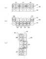
図2は、4×4画素に簡略化して描いた固体撮像素子106の回路図で、201は画像用フォトダイオード、202は画像用転送トランジスタ、203は増幅用トランジスタ、204は行選択用トランジスタ、205はリセット用トランジスタ、206は焦点検出用フォトダイオード、207は焦点検出用転送トランジスタ、210は水平走査回路、211は垂直走査回路、212は1行1列目の単位画素、213および214は単位画素212と同じ回路構成で3行1列目および4行1列目の単位画素、215は2行1列目の単位画素、216は相関二重サンプリング回路をそれぞれ示す。また、1列目の各単位画素212,215,213、214は、2列目,3列目および4列目にも同じように構成される。Next, a first embodiment of the solid-
(First embodiment)
FIG. 2 is a circuit diagram of the solid-
また、φで始まる信号名は駆動信号を表し、駆動信号のφR1,φR2,φR3およびφR4は、それぞれ順番に1行目,2行目,3行目および4行目のリセット用の駆動信号を示す。同様に、駆動信号のφS1,φS2,φS3およびφS4は、それぞれ順番に1行目,2行目,3行目および4行目の信号を垂直信号線に読み出す時の選択用の駆動信号を示し、駆動信号のφTG1,φTG21,φTG3およびφTG4は、それぞれ順番に1行目,2行目,3行目および4行目の各列の画像用フォトダイオードの電荷を各増幅用トランジスタに転送するための転送用の駆動信号を示す。また、2行目の駆動信号φTG22は、2行目の各列の焦点検出用フォトダイオードの電荷を各増幅用トランジスタに転送するための転送用の駆動信号を示す。φCは相関二重サンプリング回路216にリセットノイズ電圧をクランプする駆動信号、φRHは水平読み出し線リセット用の駆動信号、φRVは垂直信号線リセット用の駆動信号、φH1,φH2,φH3およびφH4は、それぞれ1列目,2列目,3列目および4列目の水平読み出し用の駆動信号をそれぞれ示す。尚、VRESはリセット電圧、VCSは電流源に加えられる電源、VDDは各単位画素に供給される電源電圧をそれぞれ示す。A signal name starting with φ represents a drive signal. The drive signals φR1 , φR2 , φR3 and φR4 are for resetting the first row, the second row, the third row and the fourth row, respectively. The drive signal is shown. Similarly, φS1 , φS2 , φS3, and φS4 of the drive signals are used for selection when the signals of the first row, the second row, the third row, and the fourth row are sequentially read out to the vertical signal lines, respectively. The driving signals φTG1 , φTG21 , φTG3 and φTG4 indicate the charges of the image photodiodes in the first row, second row, third row and fourth row, respectively. The drive signal for transfer for transferring to each amplification transistor is shown. The drive signal φTG22 in the second row indicates a drive signal for transfer for transferring the charge of the focus detection photodiode in each column in the second row to each amplification transistor. φC is a drive signal for clamping the reset noise voltage to correlated
ここで、単位画素215は、単位画素212,213および214と回路構成が異なり、画像用フォトダイオード201と画像用転送トランジスタ202の他に、焦点検出用フォトダイオード206と焦点検出用フォトダイオード206の電荷を転送する焦点検出用転送トランジスタ207がさらに設けられる。また、画像用フォトダイオードおよび焦点検出用フォトダイオードのいずれも、フローティングディフュージョン(FD)部、増幅用トランジスタ、リセット用トランジスタ、行選択用トランジスタを有する。これらの構成により、行選択用トランジスタがオンすると、定電流源PS1からPS4に接続されている各垂直信号線にソースフォロワ読み出しが可能となる。Here, the
次に、図2の回路図の動作を、図3および図4に示したタイミングチャートを用いて説明する。図3は画像用信号を読み出す時のタイミングを示した図で、図4は焦点検出用信号を読み出す時のタイミングを示した図である。尚、図2と同じ名称の駆動信号は同じものである。
先ず、画像信号を読み出す場合の動作を説明する。t11の期間に1行目のリセット用トランジスタ205と転送用トランジスタ202とがオンされ、画像用フォトダイオード201に蓄積された電荷がリセットされる。その後、t12,t13およびt14の期間で、転送用トランジスタ202はオフされ、画像用フォトダイオード201で露光が開始され、電荷が蓄積されていく。また、この期間、増幅用トランジスタ203のゲート及びFD部が駆動信号φR1によってリセットされ、それに対応するダークレベル、つまりリセットノイズが保持される。尚、talは露光期間を示す。Next, the operation of the circuit diagram of FIG. 2 will be described using the timing charts shown in FIGS. FIG. 3 is a diagram showing the timing when the image signal is read out, and FIG. 4 is a diagram showing the timing when the focus detection signal is read out. The drive signals having the same names as in FIG. 2 are the same.
First, an operation for reading an image signal will be described. In the period t11 , the reset transistor 205 and the
一方、t12からt16の期間で、行選択用トランジスタ204が駆動信号φS1によってオンされると、上記ダークレベルは列アンプA1からA4によって増幅されて相関二重サンプリング回路216のコンデンサに蓄積される。露光期間ta1の終了時のt15の期間で、転送用トランジスタ202が駆動信号φTG1によってオンされ、画像用フォトダイオード201に蓄積された光信号電荷がFD部および増幅用トランジスタ203のゲートに転送される。これによって、ダークレベルと光信号電荷とが重畳された電気信号が相関二重サンプリング回路216に読み出され、先にクランプしておいたダークレベルを差し引いた光信号に相当する信号だけが水平信号線に出力される。On the other hand, when the row selection transistor 204 is turned on by the drive signal φS1 in the period from t12 to t16 , the dark level is amplified by the column amplifiers A1 to A4 and the capacitor of the correlated
このように、相関二重サンプリング回路216でノイズ低減された光信号は、1列目の場合、水平走査回路210の駆動信号φH1によって読み出され、2列目はφH2,3列目はφH3,4列目はφH4によってそれぞれ読み出され、出力アンプPAを介してVSout端子から出力される。尚、図2において、φRHやφRVおよびφCなどの駆動信号を出力する制御回路は省略してある。Thus, in the first column, the optical signal whose noise has been reduced by the correlated
同様に、他の行の単位画素の画像信号が読み出され、全ての行を読み終えると、1フレームの画像信号の読み出しが終了する。尚、t21,t22,t23,t24,t25,t26およびt27は、2列目の単位画素215に対応する。1列目の単位画素212の駆動信号φR1をφR2に、φS1をφS2に、φTG1をφTG21に置き換えて、t11,t12,t13,t14,t15,t16およびt17と同様のタイミングで動作する。3列目および4列目に関しても同様である。尚、このように画像信号を出力する場合は、φTG22はいつも非選択の信号である。Similarly, when the image signals of the unit pixels in the other rows are read and all the rows have been read, the reading of the image signal for one frame is completed. Note that t21 , t22 , t23 , t24 , t25 , t26 and t27 correspond to the
次に、焦点検出用の信号を読み出す場合の動作について説明する。図2の2行目の単位画素215において、図4のt11の期間にリセット用トランジスタ205と焦点検出用転送トランジスタ207とがオンされ、焦点検出用フォトダイオード206に蓄積された電荷がリセットされる。その後、t12,t13およびt14の期間で、焦点検出用転送トランジスタ205はオフされ、焦点検出用フォトダイオード206で露光が開始され、電荷が蓄積されていく。また、この期間、増幅用トランジスタ203のゲート及びFD部が駆動信号φR2によってリセットされ、それに対応するダークレベル、つまりリセットノイズが保持される。尚、talは露光期間を示す。Next, an operation for reading a focus detection signal will be described. In the
一方、t12からt16の期間で、行選択用トランジスタ204が駆動信号φS2によってオンされると、図3で説明した画像用信号の読み出しと同様に、上記ダークレベルが相関二重サンプリング回路216のコンデンサに蓄積される。露光期間ta1の終了時のt15の期間で、焦点検出用転送トランジスタ207が駆動信号φTG22によってオンされ、焦点検出用フォトダイオード206に蓄積された焦点検出用の光信号電荷がFD部および増幅用トランジスタ203のゲートに転送される。この後の動作は、先に説明した画像用フォトダイオードの信号を読み出す場合と同じで、焦点検出用のフォトダイオードを有する単位画素がある行の読み出しを同様に繰り返す。図1の焦点検出部113は、このようにして読み出された焦点検出用の信号を用いて、瞳分割方式による焦点検出処理を行う。On the other hand, when the row selection transistor 204 is turned on by the drive signal φS2 during the period from t12 to t16 , the dark level is correlated with the correlated double sampling circuit as in the reading of the image signal described with reference to FIG. Accumulated in 216 capacitors. In the period t15 at the end of the exposure period ta1 , the focus
以上の動作により、本実施形態の固体撮像素子は、焦点検出用フォトダイオードのみの電荷を電気信号として読み出すことができるので、焦点検出に関係のない単位画素の電気信号を読み出す必要が無く、AF処理の高速化が可能になる。
尚、本実施形態では、AF専用の単位画素の信号だけを部分読出しする場合について説明しているが、全画素を順次読出し、後処理にてAF専用の単位画素の出力を取り出して、その出力データからAF処理を行うようにしても構わない。このような方法によれば、CCD型の固体撮像素子においても本発明の技術は利用できるが、ランダムアクセスが可能なCMOS型センサではAF画素の部分読み出しによる高速化が可能であるため、CMOS型の固体撮像素子の方がより好ましい。With the above operation, the solid-state imaging device of the present embodiment can read out the electric charge of only the focus detection photodiode as an electric signal, so there is no need to read out an electric signal of a unit pixel not related to focus detection, and AF The processing speed can be increased.
In this embodiment, the case where only the signal of the unit pixel dedicated to AF is partially read is described. However, all the pixels are sequentially read out, and the output of the unit pixel dedicated to AF is extracted in the post-processing and output. You may make it perform AF process from data. According to such a method, the technique of the present invention can also be used in a CCD solid-state imaging device, but a CMOS sensor capable of random access can increase the speed by partial readout of AF pixels. The solid-state imaging device is more preferable.
ここで、本実施形態による瞳分割方式の原理を説明する。図5(a)は図6(a)に示す固体撮像素子106aを切断位置(A1−A2)で切断した時の断面図である。501および502はそれぞれ隣接する単位画素のマイクロレンズである。503はマイクロレンズ直下の平坦化膜および層間膜、504は半導体基板、505および506は半導体基板504の上に形成された画像用フォトダイオード、507および508は半導体基板504の上に形成された焦点検出用フォトダイオード、509は図1のカメラレンズ102から入射する光線をそれぞれ示す。 Here, the principle of the pupil division method according to the present embodiment will be described. FIG. 5A is a cross-sectional view when the solid-
光線509において、実線で示す光線は、カメラレンズ系の光軸を中心として入射する光線で、画像用フォトダイオード505の上の点512、および画像用フォトダイオード506の上の点513にそれぞれ集光される。点線で示す光線は、カメラレンズ系の光軸を中心として紙面左側のレンズの瞳部分より入射する光線で、画像用フォトダイオード506の右側にある焦点検出用フォトダイオード508の上の点515に集光される。一点鎖線で示す光線は、カメラレンズ系の光軸を中心として紙面右側のレンズの瞳部分より入射する光線で、画像用フォトダイオード505の左側にある焦点検出用フォトダイオード507の上の点514に集光される。 In the
焦点がずれた場合には像ずれが生じるので、焦点検出用フォトダイオード507と508との出力が一致しない。合焦時は像ずれが生じないので、焦点検出用フォトダイオード507と508との出力が一致する。このように、焦点検出用フォトダイオード507と508の出力を比較することにより、像ずれ量を検出することができ、デフォーカス量の算出が可能となる。 Since the image shift occurs when the focus is shifted, the outputs of the
尚、図6(a)において、焦点検出用フォトダイオード507と508とがペアになって、瞳分割方式における一つの焦点検出単位を構成する。つまり、焦点検出の最小単位は、単位画素519と520の二つの単位画素で構成され、その最小単位を「焦点検出単位」と称す。同様に、焦点検出用フォトダイオード601と602とがペアになって、一つの焦点検出単位を構成する。 In FIG. 6A, focus
次に、一つの単位画素の中にペアとなる二つの焦点検出用フォトダイオードを有する場合の例を説明する。図5(b)は図6(b)に示す固体撮像素子106bを切断位置(B1−B2)で切断した時の断面図である。501乃至505および509は図5(a)と同じものを示し、510および511は、半導体基板504の上に形成された焦点検出用フォトダイオードである。図5(a)と異なるのは、一つの単位画素に二つの焦点検出用フォトダイオード510および511が形成されていることである。 Next, an example in the case where two focus detection photodiodes are paired in one unit pixel will be described. FIG. 5B is a cross-sectional view when the solid-
図5(b)の実線で示す光線は、カメラレンズ系の光軸を中心として入射する光線で、画像用フォトダイオード505上の点516に集光される。点線で示す光線は、カメラレンズ系の光軸を中心として紙面左側のレンズの瞳部分より入射する光線で、画像用フォトダイオード505の右側にある焦点検出用フォトダイオード511上の点518に集光される。一点鎖線で示す光線は、カメラレンズ系の光軸を中心として紙面右側のレンズの瞳部分より入射する光線で、画像用フォトダイオード505の左側にある焦点検出用フォトダイオード510上の点517に集光される。 A light beam indicated by a solid line in FIG. 5B is a light beam that enters with the optical axis of the camera lens system as the center, and is focused on a
焦点がずれた場合には像ずれが生じ、焦点検出用フォトダイオード510と511との出力が一致しない。合焦時は像ずれが生じないので、焦点検出用フォトダイオード510と511との出力が一致する。このように、焦点検出用フォトダイオード510と511との出力を比較することにより、像ずれ量を検出することができ、デフォーカス量の算出が可能となる。 When the focus is shifted, an image shift occurs, and the outputs of the
尚、図6(b)において、焦点検出用フォトダイオード510と511とがペアになって、瞳分割方式における一つの焦点検出単位を構成する。つまり、ここでは、焦点検出単位は、単位画素521の一つの単位画素で構成される。同様に、焦点検出用フォトダイオード603と604,605と606,607と608はそれぞれがペアになって一つの焦点検出単位を構成する。ここで、図6(a)では、二つの単位画素で一つの焦点検出単位を構成するのに対して、図6(b)では、一つの単位画素で一つの焦点検出単位を構成するので、焦点検出の解像度を約2倍に向上させることができる。 In FIG. 6B, the
尚、本実施形態では、1行分の単位画素に焦点検出用フォトダイオードが配置されているが、複数行であっても構わないし、隣接する単位画素でなくても、瞳分割方向であれば、複数画素跳んでいても構わない。但し、図6の各単位画素において、一対の焦点検出用フォトダイオードの瞳分割方向が、撮像エリアの中心を軸とする同心円の略接線方向に配置されていることが重要である。 In the present embodiment, the focus detection photodiodes are arranged in the unit pixels for one row. However, the focus detection photodiodes may be arranged in a plurality of rows or even in the pupil division direction even if they are not adjacent unit pixels. A plurality of pixels may be jumped. However, in each unit pixel in FIG. 6, it is important that the pupil division direction of the pair of focus detection photodiodes is arranged in a substantially tangential direction of a concentric circle with the center of the imaging area as an axis.
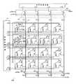
次に、複数個の焦点検出単位がまとまって配置された焦点検出用ブロック(以降、AF用画素と呼ぶ)の配置について説明する。図7は、固体撮像素子106の撮像エリア内に様々な形状のAF用画素が配置された例を示した図である。300は20×20の単位画素で構成される撮像エリア、301は撮像エリア300の中心307を軸とする同心円をそれぞれ示す。また、点線円302から306は、AF用画素の形状例を説明するために付けた符号である。撮像エリア300の中心307付近では、図13で説明したような瞳分割像のずれは少ないので、直線状のAF用画素を360度あらゆる方向に配置可能である。 Next, the arrangement of focus detection blocks (hereinafter referred to as AF pixels) in which a plurality of focus detection units are arranged together will be described. FIG. 7 is a diagram illustrating an example in which AF pixels having various shapes are arranged in the imaging area of the solid-
ところが、撮像エリア300の周辺部では、瞳分割像が撮像エリア300の中心307から放射状方向にずれる。そこで、本実施形態では、図13(a)および(b)のようにAF用画素を配置する。そこで、図7(b)において、撮像エリア300の周辺部に配置された8箇所のAF用画素は、各AF用画素の瞳分割方向が撮像エリア300の中心307を軸とする同心円301の略接線方向になるように配置される。 However, in the peripheral part of the
次に、AF用画素の配置例について説明する。図8(a)は図7のAF用画素302の部分を拡大した図である。同様に、図8(b)はAF用画素303を、図8(c)はAF用画素304を、図9(a)はAF用画素305を、図9(b)はAF用画素306をそれぞれ拡大した図を示す。また、351は同心円301上の接線を示す。
図8(a)において、311,312および313は二つの単位画素で構成される焦点検出単位で、これら三つの焦点検出単位311,312および313で一つのAF用画素302を構成する。ここで、AF用画素302の中心にある焦点検出単位312の瞳分割方向は、焦点検出単位312の中点における同心円301の接線351の方向になるように配置される。Next, an arrangement example of AF pixels will be described. FIG. 8A is an enlarged view of the
In FIG. 8A,
一方、焦点検出単位311および313の瞳分割方向は、それぞれの焦点検出単位の中点における同心円301の接線方向とは少し異なるが、実際の固体撮像素子では百万画素レベルの単位画素がアレイ状に配置されているので、固体撮像素子全体の大きさに対してAF用画素の長さが占める割合が小さければ、略接線方向に配置されているものと見なせる。 On the other hand, the pupil division direction of the
次に、図8(b)において、314から319は一つの単位画素で構成される焦点検出単位で、これら六つの焦点検出単位314から319で一つのAF用画素303を構成している。ここで、AF用画素303の中心にある二つの焦点検出単位317および318の瞳分割方向は、焦点検出単位317と318との中点における同心円301の接線351方向になるように配置される。 Next, in FIG. 8B,
一方、焦点検出単位316および319の瞳分割方向は、それぞれの焦点検出単位の中点における同心円301の接線方向とは少し異なっているが、先に説明した図8(a)の場合と同様に、AF用画素の中心付近の焦点検出単位の瞳分割方向は、略接線方向に配置されているものと見なせる。
ところが、直線状に長いAF用画素の場合は、AF用画素の中心付近の焦点検出単位が同心円301の接線方向に配置されていても、AF用画素の端部に行くにつれて、同心円301の接線方向とのずれが大きくなる。図8(b)の例の場合、AF画素303の端部の焦点検出単位314および315は、中心付近の焦点検出単位316から319に対して、撮像エリアの中心方向にずらして配置してある。このため、焦点検出単位314および315は、他の焦点検出単位316から319を通る同心円301の線上に配置でき、同心円301の接線方向とのずれの影響を少なくできる。On the other hand, the pupil division directions of the
However, in the case of an AF pixel that is linearly long, even if the focus detection units near the center of the AF pixel are arranged in the tangential direction of the
図8(c)のAF用画素304が図8(b)のAF用画素303と異なる点は、AF画素303が一つの単位画素で一つの焦点検出単位を構成しているのに対して、AF画素304は二つの単位画素で一つの焦点検出単位を構成していることである。また、図8(c)の場合も、AF用画素304の端部の焦点検出単位320と321とが、AF用画素304の中心にある焦点検出単位322に対して、撮像エリアの中心方向にずらして配置してある。このため、焦点検出単位320および321は、焦点検出単位322を通る同心円301の線上に近い位置に配置でき、同心円301の接線方向とのずれの影響を少なくできる。 The
次に、図9を用いて、その他のAF用画素の形状例について説明する。図8で説明したAF用画素302から304は、いずれも図7の撮像エリア300の水平方向または垂直方向に配置されているが、ここで説明するAF用画素305および306は、図7の撮像エリア300の角の部分に斜め方向に配置されている。
図9(a)において、323から327は一つの単位画素で構成される焦点検出単位で、これら五つの焦点検出単位323から327で一つのAF用画素305を構成する。ここで、AF用画素305の中心にある焦点検出単位325の瞳分割方向は、焦点検出単位325の中点における同心円301の接線351の方向になるように配置される。Next, other shape examples of AF pixels will be described with reference to FIG. The
In FIG. 9A,
一方、AF用画素305の中心からずれた位置にある焦点検出単位323,324,326および327の瞳分割方向は、同心円301の接線方向とは少し異なるが、図8(a)で説明したように、固体撮像素子全体の大きさに対してAF用画素の長さが占める割合が小さければ、略接線方向に配置されているものと見なせるので、同心円301の接線方向とのずれの影響は無視できる。 On the other hand, the pupil division direction of the
次に、ずれの影響を少なくしたAF用画素の例を図9(b)に示す。同図のAF用画素306は、七つの焦点検出単位328から334で構成される。AF用画素306の中心にある二つの焦点検出単位330および331の瞳分割方向は、焦点検出単位330と331との中点における同心円301の接線351の方向になるように配置される。
一方、AF用画素306の端部にある焦点検出単位328および333は、AF用画素306の中心付近の焦点検出単位329から332に対して、撮像エリアの中心方向にずらして配置してある。このため、焦点検出単位328および333は、AF用画素306の中心に位置する焦点検出単位330および331を通る同心円301の線上に近い位置に配置でき、同心円301の接線方向とのずれの影響を少なくできる。Next, FIG. 9B shows an example of an AF pixel in which the influence of deviation is reduced. The
On the other hand, the
また、AF用画素306の中点が焦点検出単位330と331との間に位置するため、焦点検出単位330および331は、同心円301の接線方向とは少しずれている。この影響を少なくするために、もう一つの焦点検出用画素334を焦点検出単位330と331との間に位置するように配置する。
このように、撮像エリア300の周辺部において、AF用画素の瞳分割方向が、撮像エリア300の中心307を軸とする同心円の略接線方向になるように配置されるので、瞳分割像がけられることなく、正確な焦点検出を行うことが可能になる。Further, since the midpoint of the
As described above, in the peripheral portion of the
(第2の実施形態)
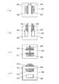
次に、本発明に係る固体撮像素子の第2の実施形態について説明する。図10は、カメラレンズ102および固体撮像素子106と、撮像エリア300の中の一つの単位画素405との位置関係を示した図である。401は固体撮像素子106の半導体基板、402は平坦化層、403はマイクロレンズ、404は半導体基板401上に形成された一対の焦点検出用フォトダイオード、404aおよび404bは一対の焦点検出用フォトダイオード404を構成するそれぞれの焦点検出用フォトダイオード、409は画像用フォトダイオード、450はカメラレンズ102と撮像エリア300との中心軸、451は単位画素405の中心軸をそれぞれ示す。尚、452の点線円は単位画素405を中心とする断面図、453の点線円は単位画素405の平面図をそれぞれ示す。(Second Embodiment)
Next, a second embodiment of the solid-state imaging device according to the present invention will be described. FIG. 10 is a diagram illustrating a positional relationship between the
ここで、焦点検出用フォトダイオード404aおよび404bは2個で一対を成し、一つの焦点検出単位を構成する。また、単位画素405において、撮像エリア300の中心を軸とする同心円の接線351の方向に瞳分割方向が来るように、焦点検出用フォトダイオード404aおよび404bが配置される。これによって、瞳分割位相差情報を取得することができ、デフォーカス量を検出することが可能となる。尚、図10では省略しているが、第1の実施形態で説明したように、複数の焦点検出単位でAF用画素を形成しても構わない。 Here, two
ここで、カメラレンズ102と固体撮像素子106の平坦化膜402の上面(マイクロレンズ403の下面)との距離(射出瞳距離)をL、撮像エリア300の中心軸450と単位画素405の中心軸との距離をr、平坦化膜402の厚さ(マイクロレンズ403の下面と焦点検出用フォトダイオード404の上面との距離)をd、単位画素405の中心軸451を通る中心線461と焦点検出用フォトダイオード404の長手方向の中心線462とのずらし量をsとした場合に、(式1)の関係が成立するように、各部を配置する。
d × (r/L) × 0.8 ≦ s ≦ d × (r/L) × 1.2 ・・・ (式1)
これにより、マイクロレンズ102の収束光がけられることなく、AF用画素の焦点検出用フォトダイオード404に集光することが可能になる。さらに、第1の実施形態で説明したように、撮像エリア300の中心を軸とする同心円の接線方向に焦点検出単位を配置することによって、瞳分割光のクロストークを抑制することができ、AF感度の低下防止やAF精度の向上を実現できる。Here, the distance (exit pupil distance) between the
d x (r / L) x 0.8 ≤ s ≤ d x (r / L) x 1.2 (Equation 1)
As a result, the convergent light from the
(第3の実施形態)
次に、本発明に係る固体撮像素子の第3の実施形態について説明する。図11は、第2の実施形態の図10と同様に、カメラレンズ102および固体撮像素子106と、撮像エリア300の中の一つの単位画素405との位置関係を示した図である。第2の実施形態と異なるのは、マイクロレンズ406と焦点検出用フォトダイオード407の位置である。つまり、単位画素405の平面図を示す点線円455において、マイクロレンズ406の中心線463は、焦点検出用フォトダイオード407および単位画素405の中心線464から、撮像エリア300の中心307に向って、ずらし量tだけずれて配置される。(Third embodiment)
Next, a third embodiment of the solid-state imaging device according to the present invention will be described. FIG. 11 is a diagram illustrating the positional relationship between the
ここで、カメラレンズ102と固体撮像素子106の平坦化膜402の上面(マイクロレンズ403の下面)との距離(射出瞳距離)をL、撮像エリア300の中心軸450と単位画素405の中心軸との距離をr、平坦化膜402の厚さ(マイクロレンズ403の下面と焦点検出用フォトダイオード404の上面との距離)をdとした場合に、(式2)の関係が成立するように、各部を配置する。
d × (r/L) × 0.8 ≦ t ≦ d × (r/L) × 1.2 ・・・ (式2)
これにより、マイクロレンズ102の収束光がけられることなく、AF用画素の焦点検出用フォトダイオード407に集光することが可能になる。第1の実施形態で説明したように、撮像エリア300の中心を軸とする同心円の接線方向に焦点検出単位を配置することによって、瞳分割光のクロストークを抑制することができ、AF感度の低下防止やAF精度の向上を実現できる。Here, the distance (exit pupil distance) between the
d x (r / L) x 0.8 ≤ t ≤ d x (r / L) x 1.2 (Formula 2)
As a result, the convergent light from the
(第4の実施形態)
次に、本発明に係る固体撮像素子の第4の実施形態について説明する。図12は、第2および第3の実施形態と同様に、カメラレンズ102および固体撮像素子106と、撮像エリア300の中の一つの単位画素405との位置関係を示した図である。マイクロレンズ403は第2の実施形態と同じように単位画素405と中心軸451を同じくする位置に配置されており、焦点検出用フォトダイオード408は第3の実施形態と同じように単位画素405と中心線465を同じくする位置に配置される。第2および第3の実施形態と異なるのは、焦点検出用フォトダイオード408の長さWが長いことである。(Fourth embodiment)
Next, a fourth embodiment of the solid-state imaging device according to the present invention will be described. FIG. 12 is a diagram showing the positional relationship between the
一つの焦点検出単位を構成する焦点検出用フォトダイオード404aおよび404bは、撮像エリア300の中心を軸とする同心円の接線351の方向に瞳分割方向が来るように、配置されているので、図13(a)および(b)で説明したように、瞳分割像804および805は焦点検出用光電変換部802および803の長手方向にずれる。ずれた場合でも、瞳分割方向は正しいので、焦点検出が可能であるが、瞳分割像がはみ出した分だけ検出信号の出力が低くなる。そこで、図12においては、焦点検出用フォトダイオード408は、長手方向に長く形成されるので、瞳分割像が焦点検出用フォトダイオード408の長手方向にずれた場合でも、焦点検出用フォトダイオードからはみ出る部分を少なくできる。 Since the
ここで、カメラレンズ102と固体撮像素子106の平坦化膜402の上面(マイクロレンズ403の下面)との距離(射出瞳距離)をL、カメラレンズ102のF値をf、撮像エリア300の中心軸450と単位画素405の中心軸との距離をr、平坦化膜402の厚さ(マイクロレンズ403の下面と焦点検出用フォトダイオード404の上面との距離)をd、焦点検出用フォトダイオード408の長さをw、とした場合に、(式3)の関係が成立するように、各部を配置する。
d/f + d × (r/L) × 0.8 ≦ w ≦ d/f + d × (r/L) × 1.2 ・・・ (式3)
これにより、マイクロレンズ102の収束光がけられることなく、AF用画素の焦点検出用フォトダイオード408に集光することが可能になる。本実施形態においても、第1の実施形態で説明した焦点検出単位の配置と複合することによって、瞳分割光のクロストークを抑制することができ、AF感度の低下防止やAF精度の向上を実現できる。Here, the distance (exit pupil distance) between the
d / f + d x (r / L) x 0.8 ≤ w ≤ d / f + d x (r / L) x 1.2 (Equation 3)
As a result, the convergent light from the
以上、各実施形態において説明してきたように、本発明に係る固体撮像素子は、撮像エリアの周辺部において、AF用画素の瞳分割方向が、撮像エリアの中心を軸とする同心円の略接線方向になるように配置されるので、瞳分割像がけられることなく、正確な焦点検出を行うことができる。
また、マイクロレンズと焦点検出用フォトダイオードの位置関係を撮像エリアの中心からの距離によって変えることによって、瞳分割像のけられを少なくすることができる。As described above, in each of the embodiments, the solid-state imaging device according to the present invention is configured so that the pupil division direction of the AF pixel is a concentric substantially tangential direction with the center of the imaging area as the axis at the periphery of the imaging area. Therefore, accurate focus detection can be performed without generating a pupil-divided image.
In addition, by changing the positional relationship between the microlens and the focus detection photodiode according to the distance from the center of the imaging area, the divergence of the pupil division image can be reduced.
さらに、焦点検出用フォトダイオードの長さを撮像エリアの中心からの距離によって変えることで、瞳分割像のけられを少なくすることができる。
或いは、上記の各実施形態を複合して実施することで、より効果的に瞳分割像のけられやクロストークを抑圧することができる。
また、上記のような本発明に係る固体撮像素子を電子カメラに利用することによって、カメラレンズの射出瞳距離等の撮像条件に影響を受けることなく、AF感度やAF精度を劣化させずに、位相差焦点検出が可能な電子カメラを実現することができる。特に、AF用画素を配置する位置に応じて、水平,垂直あるいは斜め方向など、あらゆる方向に瞳分割が可能な固体撮像素子を用いることで、高級デジタル一眼レフカメラなどで要求される多点AF機能も可能となる。Further, by changing the length of the focus detection photodiode according to the distance from the center of the imaging area, the divergence of the pupil division image can be reduced.
Alternatively, by implementing the above embodiments in combination, it is possible to more effectively suppress pupil division image shift and crosstalk.
Further, by using the solid-state imaging device according to the present invention as described above for an electronic camera, without being affected by imaging conditions such as the exit pupil distance of the camera lens, without deteriorating the AF sensitivity or AF accuracy, An electronic camera capable of phase difference focus detection can be realized. In particular, multi-point AF required for high-end digital single-lens reflex cameras and the like by using a solid-state imaging device that can divide pupils in all directions, such as horizontal, vertical, or diagonal directions, depending on the position where AF pixels are arranged. Functions are also possible.
101・・・電子カメラ 102・・・カメラレンズ
106・・・固体撮像素子 113・・・焦点検出部
300・・・撮像エリア 301・・・同心円
302,303,304,305,306・・・AF用画素
307・・・撮像エリア300の中心
311〜334・・・焦点検出単位
351・・・同心円301の接線
403,406・・・マイクロレンズ 405・・・単位画素
404,407,408・・・焦点検出用フォトダイオード
DESCRIPTION OF
Claims (10)
Translated fromJapanese前記単位画素の中に少なくとも一つの焦点検出用光電変換部を有し、一つまたは二つの単位画素で瞳分割の1単位を構成し、且つ、前記撮像エリアの中心を軸とする同心円の略接線方向が瞳分割方向になるように前記焦点検出用光電変換部が配置された焦点検出単位と
を有する固体撮像素子。Unit pixels arranged in a matrix in the imaging area and having an image photoelectric conversion unit;
The unit pixel has at least one focus detection photoelectric conversion unit, one or two unit pixels form one unit of pupil division, and a concentric circle with the center of the imaging area as an axis. And a focus detection unit in which the focus detection photoelectric conversion unit is arranged so that a tangential direction is a pupil division direction.
前記焦点検出用ブロックの中心に位置する前記焦点検出単位の前記焦点検出用光電変換部が、前記撮像エリアの中心を軸とする同心円の略接線方向が瞳分割方向になるように配置され、
前記焦点検出用ブロックの中心以外に位置する前記焦点検出単位の前記焦点検出用光電変換部は、前記焦点検出用ブロックの中心に位置する前記焦点検出単位の前記焦点検出用光電変換部と画素内の配置の位置が同一であることを特徴とする請求項1に記載の固体撮像素子。Construct a focus detection block consisting of a plurality of consecutive focus detection units,
The focus detection photoelectric conversion unit of the focus detection unit located at the center of the focus detection block is disposed so that a substantially tangential direction of a concentric circle with the center of the imaging area as an axis is a pupil division direction.
The focus detection photoelectric conversion unit of the focus detection unit located outside the center of the focus detection block is connected to the focus detection photoelectric conversion unit of the focus detection unit located in the center of the focus detection block. The solid-state imaging device according to claim 1, wherein the positions of the two are the same.
前記焦点検出単位の前記マイクロレンズが、前記撮像エリアの中心を軸とする略同心円状に配置されたことを特徴とする請求項1乃至4のいずれか一項に記載の固体撮像素子。A microlens is provided in the unit pixel,
5. The solid-state imaging device according to claim 1, wherein the microlenses of the focus detection unit are arranged in a substantially concentric shape with the center of the imaging area as an axis.
前記カメラレンズの射出瞳距離をL、前記撮像エリアの中心から前記焦点検出用光電変換部までの距離をr、前記マイクロレンズと前記焦点検出用光電変換部との距離をdとした時に、
前記撮像エリアの中心軸に対するマイクロレンズずらし量sとの関係が
d × (r/L) × 0.8 ≦ s ≦ d × (r/L) × 1.2
で表されるようにマイクロレンズを配置したことを特徴とする請求項5に記載の固体撮像素子。When using a camera lens for the solid-state imaging device,
When the exit pupil distance of the camera lens is L, the distance from the center of the imaging area to the focus detection photoelectric conversion unit is r, and the distance between the micro lens and the focus detection photoelectric conversion unit is d,
The relationship between the microlens shift amount s with respect to the central axis of the imaging area is
d × (r / L) × 0.8 ≤ s ≤ d × (r / L) × 1.2
The solid-state imaging device according to claim 5, wherein microlenses are arranged as represented by:
前記カメラレンズの射出瞳距離をL、前記撮像エリアの中心から前記焦点検出用光電変換部までの距離をr、前記マイクロレンズと前記焦点検出用光電変換部との距離をdとした時に、
前記マイクロレンズに対する前記焦点検出用光電変換部のずらし量tとの関係が
d × (r/L) × 0.8 ≦ t ≦ d × (r/L) × 1.2
で表されるように前記焦点検出用光電変換部を配置したことを特徴とする請求項5に記載の固体撮像素子。When using a camera lens for the solid-state imaging device,
When the exit pupil distance of the camera lens is L, the distance from the center of the imaging area to the focus detection photoelectric conversion unit is r, and the distance between the micro lens and the focus detection photoelectric conversion unit is d,
The relationship with the shift amount t of the focus detection photoelectric conversion unit with respect to the microlens is
d × (r / L) × 0.8 ≦ t ≦ d × (r / L) × 1.2
The solid-state imaging device according to claim 5, wherein the focus detection photoelectric conversion unit is arranged as represented by:
d/f + d × (r/L) × 0.8 ≦ w ≦ d/f + d × (r/L) × 1.2
で表されるように前記焦点検出用光電変換部を配置したことを特徴とする請求項8に記載の固体撮像素子。In the case where a camera lens is used for the solid-state imaging device, the shape of the focus detection photoelectric conversion unit is such that the length in the radial direction from the center of the imaging area is w, the exit pupil distance of the camera lens is L, When the F value of the camera lens is f, the distance from the center of the imaging area to the focus detection photoelectric conversion unit is r, and the distance between the microlens and the focus detection photoelectric conversion unit is d,
d / f + d × (r / L) × 0.8 ≦ w ≦ d / f + d × (r / L) × 1.2
The solid-state imaging device according to claim 8, wherein the focus detection photoelectric conversion unit is arranged as represented by:
前記画像用光電変換部から電気信号を読み出すための第1の読み出し手段と、
前記焦点検出用光電変換部から電気信号を読み出すための第2の読み出し手段と、
前記第2の読み出し手段が読み出した電気信号に従って焦点制御を行う焦点制御手段と
を少なくとも備えることを特徴とする電子カメラ。
A solid-state imaging device according to any one of claims 1 to 9,
First reading means for reading an electrical signal from the image photoelectric conversion unit;
Second reading means for reading an electrical signal from the focus detection photoelectric conversion unit;
An electronic camera comprising: at least focus control means for performing focus control in accordance with the electrical signal read by the second reading means.
Priority Applications (1)
| Application Number | Priority Date | Filing Date | Title |
|---|---|---|---|
| JP2006002640AJP4935078B2 (en) | 2006-01-10 | 2006-01-10 | Solid-state imaging device and electronic camera using the same |
Applications Claiming Priority (1)
| Application Number | Priority Date | Filing Date | Title |
|---|---|---|---|
| JP2006002640AJP4935078B2 (en) | 2006-01-10 | 2006-01-10 | Solid-state imaging device and electronic camera using the same |
Publications (2)
| Publication Number | Publication Date |
|---|---|
| JP2007184840Atrue JP2007184840A (en) | 2007-07-19 |
| JP4935078B2 JP4935078B2 (en) | 2012-05-23 |
Family
ID=38340529
Family Applications (1)
| Application Number | Title | Priority Date | Filing Date |
|---|---|---|---|
| JP2006002640AExpired - Fee RelatedJP4935078B2 (en) | 2006-01-10 | 2006-01-10 | Solid-state imaging device and electronic camera using the same |
Country Status (1)
| Country | Link |
|---|---|
| JP (1) | JP4935078B2 (en) |
Cited By (16)
| Publication number | Priority date | Publication date | Assignee | Title |
|---|---|---|---|---|
| JP2009075407A (en)* | 2007-09-21 | 2009-04-09 | Nikon Corp | Imaging device |
| JP2009089132A (en)* | 2007-10-01 | 2009-04-23 | Nikon Corp | Solid-state imaging device |
| JP2009109631A (en)* | 2007-10-29 | 2009-05-21 | Sony Corp | Imaging device |
| JP2009139795A (en)* | 2007-12-10 | 2009-06-25 | Sony Corp | Imaging device |
| JP2010050513A (en)* | 2008-08-19 | 2010-03-04 | Rohm Co Ltd | Live-view capable camera |
| JP2010048857A (en)* | 2008-08-19 | 2010-03-04 | Rohm Co Ltd | Automatic focusing camera |
| WO2010021342A3 (en)* | 2008-08-19 | 2010-05-06 | ローム株式会社 | Camera |
| WO2010055931A1 (en)* | 2008-11-11 | 2010-05-20 | Canon Kabushiki Kaisha | Focus detection apparatus and control method therefor |
| JP2010169709A (en)* | 2009-01-20 | 2010-08-05 | Sony Corp | Imaging element and imaging apparatus |
| WO2012020632A1 (en)* | 2010-08-09 | 2012-02-16 | Canon Kabushiki Kaisha | Image capture apparatus |
| US8319870B2 (en) | 2008-02-22 | 2012-11-27 | Panasonic Corporation | Imaging apparatus |
| JP2013140380A (en)* | 2013-02-12 | 2013-07-18 | Nikon Corp | Imaging apparatus |
| JP2015073072A (en)* | 2013-07-11 | 2015-04-16 | キヤノン株式会社 | Solid-state imaging device and imaging apparatus using the same |
| US9160942B2 (en) | 2013-07-11 | 2015-10-13 | Canon Kabushiki Kaisha | Solid-state imaging sensor, ranging device, and imaging apparatus |
| JP2015232676A (en)* | 2014-06-11 | 2015-12-24 | キヤノン株式会社 | IMAGING DEVICE, IMAGING DEVICE CONTROL METHOD, PROGRAM, AND STORAGE MEDIUM |
| US9568606B2 (en) | 2012-03-29 | 2017-02-14 | Canon Kabushiki Kaisha | Imaging apparatus for distance detection using high and low sensitivity sensors with inverted positional relations |
Citations (8)
| Publication number | Priority date | Publication date | Assignee | Title |
|---|---|---|---|---|
| JPH05346556A (en)* | 1992-06-12 | 1993-12-27 | Victor Co Of Japan Ltd | Solid image pickup element |
| JPH07333488A (en)* | 1994-06-06 | 1995-12-22 | Nikon Corp | Focus detection device |
| JPH11281884A (en)* | 1998-03-30 | 1999-10-15 | Minolta Co Ltd | Focus position detecting device |
| JP2000292686A (en)* | 1999-04-06 | 2000-10-20 | Olympus Optical Co Ltd | Imaging device |
| JP2002131623A (en)* | 2000-10-24 | 2002-05-09 | Canon Inc | Imaging device and imaging system |
| JP2002165126A (en)* | 2000-11-28 | 2002-06-07 | Canon Inc | Imaging device, imaging system, and imaging method |
| JP2002333570A (en)* | 2001-05-09 | 2002-11-22 | Canon Inc | Imaging device, camera, and method of controlling imaging device |
| JP2004138968A (en)* | 2002-10-21 | 2004-05-13 | Canon Inc | Focus detection device |
- 2006
- 2006-01-10JPJP2006002640Apatent/JP4935078B2/ennot_activeExpired - Fee Related
Patent Citations (8)
| Publication number | Priority date | Publication date | Assignee | Title |
|---|---|---|---|---|
| JPH05346556A (en)* | 1992-06-12 | 1993-12-27 | Victor Co Of Japan Ltd | Solid image pickup element |
| JPH07333488A (en)* | 1994-06-06 | 1995-12-22 | Nikon Corp | Focus detection device |
| JPH11281884A (en)* | 1998-03-30 | 1999-10-15 | Minolta Co Ltd | Focus position detecting device |
| JP2000292686A (en)* | 1999-04-06 | 2000-10-20 | Olympus Optical Co Ltd | Imaging device |
| JP2002131623A (en)* | 2000-10-24 | 2002-05-09 | Canon Inc | Imaging device and imaging system |
| JP2002165126A (en)* | 2000-11-28 | 2002-06-07 | Canon Inc | Imaging device, imaging system, and imaging method |
| JP2002333570A (en)* | 2001-05-09 | 2002-11-22 | Canon Inc | Imaging device, camera, and method of controlling imaging device |
| JP2004138968A (en)* | 2002-10-21 | 2004-05-13 | Canon Inc | Focus detection device |
Cited By (25)
| Publication number | Priority date | Publication date | Assignee | Title |
|---|---|---|---|---|
| JP2009075407A (en)* | 2007-09-21 | 2009-04-09 | Nikon Corp | Imaging device |
| JP2009089132A (en)* | 2007-10-01 | 2009-04-23 | Nikon Corp | Solid-state imaging device |
| JP2009109631A (en)* | 2007-10-29 | 2009-05-21 | Sony Corp | Imaging device |
| JP2009139795A (en)* | 2007-12-10 | 2009-06-25 | Sony Corp | Imaging device |
| US8218962B2 (en) | 2007-12-10 | 2012-07-10 | Sony Corporation | Image-capturing apparatus |
| US8319870B2 (en) | 2008-02-22 | 2012-11-27 | Panasonic Corporation | Imaging apparatus |
| WO2010021342A3 (en)* | 2008-08-19 | 2010-05-06 | ローム株式会社 | Camera |
| US8629916B2 (en) | 2008-08-19 | 2014-01-14 | Rohm Co., Ltd. | Camera with imaging unit and imaging unit for camera |
| JP2010048857A (en)* | 2008-08-19 | 2010-03-04 | Rohm Co Ltd | Automatic focusing camera |
| JP2010050513A (en)* | 2008-08-19 | 2010-03-04 | Rohm Co Ltd | Live-view capable camera |
| WO2010055931A1 (en)* | 2008-11-11 | 2010-05-20 | Canon Kabushiki Kaisha | Focus detection apparatus and control method therefor |
| JP2010140013A (en)* | 2008-11-11 | 2010-06-24 | Canon Inc | Focus detection device and control method therefor |
| US20110199506A1 (en)* | 2008-11-11 | 2011-08-18 | Canon Kabushiki Kaisha | Focus detection apparatus and control method therefor |
| US8576329B2 (en) | 2008-11-11 | 2013-11-05 | Canon Kabushiki Kaisha | Focus detection apparatus and control method therefor |
| JP2010169709A (en)* | 2009-01-20 | 2010-08-05 | Sony Corp | Imaging element and imaging apparatus |
| JP2012037777A (en)* | 2010-08-09 | 2012-02-23 | Canon Inc | Imaging device |
| WO2012020632A1 (en)* | 2010-08-09 | 2012-02-16 | Canon Kabushiki Kaisha | Image capture apparatus |
| US8970773B2 (en) | 2010-08-09 | 2015-03-03 | Canon Kabushiki Kaisha | Image capture apparatus with first and second pixel groups |
| US9568606B2 (en) | 2012-03-29 | 2017-02-14 | Canon Kabushiki Kaisha | Imaging apparatus for distance detection using high and low sensitivity sensors with inverted positional relations |
| JP2013140380A (en)* | 2013-02-12 | 2013-07-18 | Nikon Corp | Imaging apparatus |
| JP2015073072A (en)* | 2013-07-11 | 2015-04-16 | キヤノン株式会社 | Solid-state imaging device and imaging apparatus using the same |
| US9160942B2 (en) | 2013-07-11 | 2015-10-13 | Canon Kabushiki Kaisha | Solid-state imaging sensor, ranging device, and imaging apparatus |
| US9319607B2 (en) | 2013-07-11 | 2016-04-19 | Canon Kabushiki Kaisha | Solid-state imaging sensor, ranging device, and imaging apparatus |
| US9402041B2 (en) | 2013-07-11 | 2016-07-26 | Canon Kabushiki Kaisha | Solid-state image sensor and imaging apparatus using same |
| JP2015232676A (en)* | 2014-06-11 | 2015-12-24 | キヤノン株式会社 | IMAGING DEVICE, IMAGING DEVICE CONTROL METHOD, PROGRAM, AND STORAGE MEDIUM |
Also Published As
| Publication number | Publication date |
|---|---|
| JP4935078B2 (en) | 2012-05-23 |
Similar Documents
| Publication | Publication Date | Title |
|---|---|---|
| JP4935078B2 (en) | Solid-state imaging device and electronic camera using the same | |
| JP5422889B2 (en) | Solid-state imaging device and imaging apparatus using the same | |
| JP5157436B2 (en) | Solid-state imaging device and imaging apparatus | |
| US8576329B2 (en) | Focus detection apparatus and control method therefor | |
| US8063978B2 (en) | Image pickup device, focus detection device, image pickup apparatus, method for manufacturing image pickup device, method for manufacturing focus detection device, and method for manufacturing image pickup apparatus | |
| KR102261981B1 (en) | Solid-state image pickup device and driving method therefor, and electronic apparatus | |
| JP4968893B2 (en) | Imaging device and imaging system | |
| JP4957413B2 (en) | Solid-state imaging device and imaging apparatus using the same | |
| JP5076528B2 (en) | Photoelectric conversion unit connection / separation structure, solid-state imaging device, and imaging apparatus | |
| JP5693082B2 (en) | Imaging device | |
| RU2490715C1 (en) | Image capturing device | |
| JP2007158692A (en) | Solid-state imaging device and electronic camera using the same | |
| JP5076416B2 (en) | Imaging device and imaging apparatus | |
| TW201515467A (en) | Solid-state imaging device, driving method thereof, and electronic device | |
| JP2005106994A (en) | Focus detection apparatus, imaging apparatus, and control method thereof | |
| JP4946294B2 (en) | Imaging device and imaging apparatus | |
| JP2011221254A (en) | Imaging device, solid-state image pick-up element, imaging method and program | |
| CN102089698A (en) | Image-capturing apparatus | |
| JP5023480B2 (en) | Electronic camera | |
| JP5211590B2 (en) | Image sensor and focus detection apparatus | |
| JP2002199284A (en) | Image pickup element | |
| JP2014165778A (en) | Solid state image sensor, imaging device and focus detector | |
| JP2001210812A (en) | Solid-state imaging device and solid-state imaging system having the same | |
| JP4567712B2 (en) | Imaging device | |
| JP5750918B2 (en) | Solid-state imaging device and imaging apparatus using the same |
Legal Events
| Date | Code | Title | Description |
|---|---|---|---|
| A621 | Written request for application examination | Free format text:JAPANESE INTERMEDIATE CODE: A621 Effective date:20081204 | |
| A977 | Report on retrieval | Free format text:JAPANESE INTERMEDIATE CODE: A971007 Effective date:20101213 | |
| A131 | Notification of reasons for refusal | Free format text:JAPANESE INTERMEDIATE CODE: A131 Effective date:20101221 | |
| A521 | Request for written amendment filed | Free format text:JAPANESE INTERMEDIATE CODE: A523 Effective date:20110128 | |
| A131 | Notification of reasons for refusal | Free format text:JAPANESE INTERMEDIATE CODE: A131 Effective date:20110215 | |
| A521 | Request for written amendment filed | Free format text:JAPANESE INTERMEDIATE CODE: A523 Effective date:20110412 | |
| A131 | Notification of reasons for refusal | Free format text:JAPANESE INTERMEDIATE CODE: A131 Effective date:20111108 | |
| A521 | Request for written amendment filed | Free format text:JAPANESE INTERMEDIATE CODE: A523 Effective date:20111221 | |
| TRDD | Decision of grant or rejection written | ||
| A01 | Written decision to grant a patent or to grant a registration (utility model) | Free format text:JAPANESE INTERMEDIATE CODE: A01 Effective date:20120124 | |
| A01 | Written decision to grant a patent or to grant a registration (utility model) | Free format text:JAPANESE INTERMEDIATE CODE: A01 | |
| A61 | First payment of annual fees (during grant procedure) | Free format text:JAPANESE INTERMEDIATE CODE: A61 Effective date:20120206 | |
| FPAY | Renewal fee payment (event date is renewal date of database) | Free format text:PAYMENT UNTIL: 20150302 Year of fee payment:3 | |
| R150 | Certificate of patent or registration of utility model | Ref document number:4935078 Country of ref document:JP Free format text:JAPANESE INTERMEDIATE CODE: R150 Free format text:JAPANESE INTERMEDIATE CODE: R150 | |
| FPAY | Renewal fee payment (event date is renewal date of database) | Free format text:PAYMENT UNTIL: 20150302 Year of fee payment:3 | |
| R250 | Receipt of annual fees | Free format text:JAPANESE INTERMEDIATE CODE: R250 | |
| R250 | Receipt of annual fees | Free format text:JAPANESE INTERMEDIATE CODE: R250 | |
| R250 | Receipt of annual fees | Free format text:JAPANESE INTERMEDIATE CODE: R250 | |
| R250 | Receipt of annual fees | Free format text:JAPANESE INTERMEDIATE CODE: R250 | |
| R250 | Receipt of annual fees | Free format text:JAPANESE INTERMEDIATE CODE: R250 | |
| LAPS | Cancellation because of no payment of annual fees |