JP2007184414A - Semiconductor device mounting substrate, semiconductor device and electronic apparatus - Google Patents
Semiconductor device mounting substrate, semiconductor device and electronic apparatusDownload PDFInfo
- Publication number
- JP2007184414A JP2007184414AJP2006001586AJP2006001586AJP2007184414AJP 2007184414 AJP2007184414 AJP 2007184414AJP 2006001586 AJP2006001586 AJP 2006001586AJP 2006001586 AJP2006001586 AJP 2006001586AJP 2007184414 AJP2007184414 AJP 2007184414A
- Authority
- JP
- Japan
- Prior art keywords
- semiconductor element
- semiconductor device
- die pattern
- substrate
- conductor
- Prior art date
- Legal status (The legal status is an assumption and is not a legal conclusion. Google has not performed a legal analysis and makes no representation as to the accuracy of the status listed.)
- Pending
Links
Images


Classifications
- H—ELECTRICITY
- H01—ELECTRIC ELEMENTS
- H01L—SEMICONDUCTOR DEVICES NOT COVERED BY CLASS H10
- H01L25/00—Assemblies consisting of a plurality of semiconductor or other solid state devices
- H01L25/03—Assemblies consisting of a plurality of semiconductor or other solid state devices all the devices being of a type provided for in a single subclass of subclasses H10B, H10D, H10F, H10H, H10K or H10N, e.g. assemblies of rectifier diodes
- H01L25/04—Assemblies consisting of a plurality of semiconductor or other solid state devices all the devices being of a type provided for in a single subclass of subclasses H10B, H10D, H10F, H10H, H10K or H10N, e.g. assemblies of rectifier diodes the devices not having separate containers
- H01L25/065—Assemblies consisting of a plurality of semiconductor or other solid state devices all the devices being of a type provided for in a single subclass of subclasses H10B, H10D, H10F, H10H, H10K or H10N, e.g. assemblies of rectifier diodes the devices not having separate containers the devices being of a type provided for in group H10D89/00
- H01L25/0655—Assemblies consisting of a plurality of semiconductor or other solid state devices all the devices being of a type provided for in a single subclass of subclasses H10B, H10D, H10F, H10H, H10K or H10N, e.g. assemblies of rectifier diodes the devices not having separate containers the devices being of a type provided for in group H10D89/00 the devices being arranged next to each other
- H—ELECTRICITY
- H01—ELECTRIC ELEMENTS
- H01L—SEMICONDUCTOR DEVICES NOT COVERED BY CLASS H10
- H01L23/00—Details of semiconductor or other solid state devices
- H01L23/28—Encapsulations, e.g. encapsulating layers, coatings, e.g. for protection
- H01L23/31—Encapsulations, e.g. encapsulating layers, coatings, e.g. for protection characterised by the arrangement or shape
- H01L23/3107—Encapsulations, e.g. encapsulating layers, coatings, e.g. for protection characterised by the arrangement or shape the device being completely enclosed
- H01L23/3142—Sealing arrangements between parts, e.g. adhesion promotors
- H—ELECTRICITY
- H01—ELECTRIC ELEMENTS
- H01L—SEMICONDUCTOR DEVICES NOT COVERED BY CLASS H10
- H01L23/00—Details of semiconductor or other solid state devices
- H01L23/52—Arrangements for conducting electric current within the device in operation from one component to another, i.e. interconnections, e.g. wires, lead frames
- H01L23/538—Arrangements for conducting electric current within the device in operation from one component to another, i.e. interconnections, e.g. wires, lead frames the interconnection structure between a plurality of semiconductor chips being formed on, or in, insulating substrates
- H01L23/5384—Conductive vias through the substrate with or without pins, e.g. buried coaxial conductors
- H—ELECTRICITY
- H01—ELECTRIC ELEMENTS
- H01L—SEMICONDUCTOR DEVICES NOT COVERED BY CLASS H10
- H01L23/00—Details of semiconductor or other solid state devices
- H01L23/52—Arrangements for conducting electric current within the device in operation from one component to another, i.e. interconnections, e.g. wires, lead frames
- H01L23/538—Arrangements for conducting electric current within the device in operation from one component to another, i.e. interconnections, e.g. wires, lead frames the interconnection structure between a plurality of semiconductor chips being formed on, or in, insulating substrates
- H01L23/5386—Geometry or layout of the interconnection structure
- H—ELECTRICITY
- H01—ELECTRIC ELEMENTS
- H01L—SEMICONDUCTOR DEVICES NOT COVERED BY CLASS H10
- H01L24/00—Arrangements for connecting or disconnecting semiconductor or solid-state bodies; Methods or apparatus related thereto
- H01L24/01—Means for bonding being attached to, or being formed on, the surface to be connected, e.g. chip-to-package, die-attach, "first-level" interconnects; Manufacturing methods related thereto
- H01L24/26—Layer connectors, e.g. plate connectors, solder or adhesive layers; Manufacturing methods related thereto
- H01L24/31—Structure, shape, material or disposition of the layer connectors after the connecting process
- H01L24/32—Structure, shape, material or disposition of the layer connectors after the connecting process of an individual layer connector
- H—ELECTRICITY
- H01—ELECTRIC ELEMENTS
- H01L—SEMICONDUCTOR DEVICES NOT COVERED BY CLASS H10
- H01L24/00—Arrangements for connecting or disconnecting semiconductor or solid-state bodies; Methods or apparatus related thereto
- H01L24/01—Means for bonding being attached to, or being formed on, the surface to be connected, e.g. chip-to-package, die-attach, "first-level" interconnects; Manufacturing methods related thereto
- H01L24/42—Wire connectors; Manufacturing methods related thereto
- H01L24/47—Structure, shape, material or disposition of the wire connectors after the connecting process
- H01L24/49—Structure, shape, material or disposition of the wire connectors after the connecting process of a plurality of wire connectors
- H—ELECTRICITY
- H01—ELECTRIC ELEMENTS
- H01L—SEMICONDUCTOR DEVICES NOT COVERED BY CLASS H10
- H01L2224/00—Indexing scheme for arrangements for connecting or disconnecting semiconductor or solid-state bodies and methods related thereto as covered by H01L24/00
- H01L2224/01—Means for bonding being attached to, or being formed on, the surface to be connected, e.g. chip-to-package, die-attach, "first-level" interconnects; Manufacturing methods related thereto
- H01L2224/02—Bonding areas; Manufacturing methods related thereto
- H01L2224/04—Structure, shape, material or disposition of the bonding areas prior to the connecting process
- H01L2224/05—Structure, shape, material or disposition of the bonding areas prior to the connecting process of an individual bonding area
- H01L2224/0554—External layer
- H01L2224/0555—Shape
- H01L2224/05552—Shape in top view
- H01L2224/05553—Shape in top view being rectangular
- H—ELECTRICITY
- H01—ELECTRIC ELEMENTS
- H01L—SEMICONDUCTOR DEVICES NOT COVERED BY CLASS H10
- H01L2224/00—Indexing scheme for arrangements for connecting or disconnecting semiconductor or solid-state bodies and methods related thereto as covered by H01L24/00
- H01L2224/01—Means for bonding being attached to, or being formed on, the surface to be connected, e.g. chip-to-package, die-attach, "first-level" interconnects; Manufacturing methods related thereto
- H01L2224/02—Bonding areas; Manufacturing methods related thereto
- H01L2224/04—Structure, shape, material or disposition of the bonding areas prior to the connecting process
- H01L2224/05—Structure, shape, material or disposition of the bonding areas prior to the connecting process of an individual bonding area
- H01L2224/0554—External layer
- H01L2224/0555—Shape
- H01L2224/05552—Shape in top view
- H01L2224/05554—Shape in top view being square
- H—ELECTRICITY
- H01—ELECTRIC ELEMENTS
- H01L—SEMICONDUCTOR DEVICES NOT COVERED BY CLASS H10
- H01L2224/00—Indexing scheme for arrangements for connecting or disconnecting semiconductor or solid-state bodies and methods related thereto as covered by H01L24/00
- H01L2224/01—Means for bonding being attached to, or being formed on, the surface to be connected, e.g. chip-to-package, die-attach, "first-level" interconnects; Manufacturing methods related thereto
- H01L2224/26—Layer connectors, e.g. plate connectors, solder or adhesive layers; Manufacturing methods related thereto
- H01L2224/28—Structure, shape, material or disposition of the layer connectors prior to the connecting process
- H01L2224/29—Structure, shape, material or disposition of the layer connectors prior to the connecting process of an individual layer connector
- H01L2224/29001—Core members of the layer connector
- H01L2224/29099—Material
- H01L2224/2919—Material with a principal constituent of the material being a polymer, e.g. polyester, phenolic based polymer, epoxy
- H—ELECTRICITY
- H01—ELECTRIC ELEMENTS
- H01L—SEMICONDUCTOR DEVICES NOT COVERED BY CLASS H10
- H01L2224/00—Indexing scheme for arrangements for connecting or disconnecting semiconductor or solid-state bodies and methods related thereto as covered by H01L24/00
- H01L2224/01—Means for bonding being attached to, or being formed on, the surface to be connected, e.g. chip-to-package, die-attach, "first-level" interconnects; Manufacturing methods related thereto
- H01L2224/26—Layer connectors, e.g. plate connectors, solder or adhesive layers; Manufacturing methods related thereto
- H01L2224/28—Structure, shape, material or disposition of the layer connectors prior to the connecting process
- H01L2224/29—Structure, shape, material or disposition of the layer connectors prior to the connecting process of an individual layer connector
- H01L2224/29001—Core members of the layer connector
- H01L2224/29099—Material
- H01L2224/29198—Material with a principal constituent of the material being a combination of two or more materials in the form of a matrix with a filler, i.e. being a hybrid material, e.g. segmented structures, foams
- H01L2224/29199—Material of the matrix
- H01L2224/2929—Material of the matrix with a principal constituent of the material being a polymer, e.g. polyester, phenolic based polymer, epoxy
- H—ELECTRICITY
- H01—ELECTRIC ELEMENTS
- H01L—SEMICONDUCTOR DEVICES NOT COVERED BY CLASS H10
- H01L2224/00—Indexing scheme for arrangements for connecting or disconnecting semiconductor or solid-state bodies and methods related thereto as covered by H01L24/00
- H01L2224/01—Means for bonding being attached to, or being formed on, the surface to be connected, e.g. chip-to-package, die-attach, "first-level" interconnects; Manufacturing methods related thereto
- H01L2224/26—Layer connectors, e.g. plate connectors, solder or adhesive layers; Manufacturing methods related thereto
- H01L2224/28—Structure, shape, material or disposition of the layer connectors prior to the connecting process
- H01L2224/29—Structure, shape, material or disposition of the layer connectors prior to the connecting process of an individual layer connector
- H01L2224/29001—Core members of the layer connector
- H01L2224/29099—Material
- H01L2224/29198—Material with a principal constituent of the material being a combination of two or more materials in the form of a matrix with a filler, i.e. being a hybrid material, e.g. segmented structures, foams
- H01L2224/29298—Fillers
- H01L2224/29299—Base material
- H01L2224/293—Base material with a principal constituent of the material being a metal or a metalloid, e.g. boron [B], silicon [Si], germanium [Ge], arsenic [As], antimony [Sb], tellurium [Te] and polonium [Po], and alloys thereof
- H01L2224/29338—Base material with a principal constituent of the material being a metal or a metalloid, e.g. boron [B], silicon [Si], germanium [Ge], arsenic [As], antimony [Sb], tellurium [Te] and polonium [Po], and alloys thereof the principal constituent melting at a temperature of greater than or equal to 950°C and less than 1550°C
- H01L2224/29339—Silver [Ag] as principal constituent
- H—ELECTRICITY
- H01—ELECTRIC ELEMENTS
- H01L—SEMICONDUCTOR DEVICES NOT COVERED BY CLASS H10
- H01L2224/00—Indexing scheme for arrangements for connecting or disconnecting semiconductor or solid-state bodies and methods related thereto as covered by H01L24/00
- H01L2224/01—Means for bonding being attached to, or being formed on, the surface to be connected, e.g. chip-to-package, die-attach, "first-level" interconnects; Manufacturing methods related thereto
- H01L2224/26—Layer connectors, e.g. plate connectors, solder or adhesive layers; Manufacturing methods related thereto
- H01L2224/31—Structure, shape, material or disposition of the layer connectors after the connecting process
- H01L2224/32—Structure, shape, material or disposition of the layer connectors after the connecting process of an individual layer connector
- H01L2224/3205—Shape
- H01L2224/32057—Shape in side view
- H—ELECTRICITY
- H01—ELECTRIC ELEMENTS
- H01L—SEMICONDUCTOR DEVICES NOT COVERED BY CLASS H10
- H01L2224/00—Indexing scheme for arrangements for connecting or disconnecting semiconductor or solid-state bodies and methods related thereto as covered by H01L24/00
- H01L2224/01—Means for bonding being attached to, or being formed on, the surface to be connected, e.g. chip-to-package, die-attach, "first-level" interconnects; Manufacturing methods related thereto
- H01L2224/26—Layer connectors, e.g. plate connectors, solder or adhesive layers; Manufacturing methods related thereto
- H01L2224/31—Structure, shape, material or disposition of the layer connectors after the connecting process
- H01L2224/32—Structure, shape, material or disposition of the layer connectors after the connecting process of an individual layer connector
- H01L2224/321—Disposition
- H01L2224/32151—Disposition the layer connector connecting between a semiconductor or solid-state body and an item not being a semiconductor or solid-state body, e.g. chip-to-substrate, chip-to-passive
- H01L2224/32221—Disposition the layer connector connecting between a semiconductor or solid-state body and an item not being a semiconductor or solid-state body, e.g. chip-to-substrate, chip-to-passive the body and the item being stacked
- H01L2224/32225—Disposition the layer connector connecting between a semiconductor or solid-state body and an item not being a semiconductor or solid-state body, e.g. chip-to-substrate, chip-to-passive the body and the item being stacked the item being non-metallic, e.g. insulating substrate with or without metallisation
- H—ELECTRICITY
- H01—ELECTRIC ELEMENTS
- H01L—SEMICONDUCTOR DEVICES NOT COVERED BY CLASS H10
- H01L2224/00—Indexing scheme for arrangements for connecting or disconnecting semiconductor or solid-state bodies and methods related thereto as covered by H01L24/00
- H01L2224/01—Means for bonding being attached to, or being formed on, the surface to be connected, e.g. chip-to-package, die-attach, "first-level" interconnects; Manufacturing methods related thereto
- H01L2224/42—Wire connectors; Manufacturing methods related thereto
- H01L2224/44—Structure, shape, material or disposition of the wire connectors prior to the connecting process
- H01L2224/45—Structure, shape, material or disposition of the wire connectors prior to the connecting process of an individual wire connector
- H01L2224/45001—Core members of the connector
- H01L2224/45099—Material
- H01L2224/451—Material with a principal constituent of the material being a metal or a metalloid, e.g. boron (B), silicon (Si), germanium (Ge), arsenic (As), antimony (Sb), tellurium (Te) and polonium (Po), and alloys thereof
- H01L2224/45138—Material with a principal constituent of the material being a metal or a metalloid, e.g. boron (B), silicon (Si), germanium (Ge), arsenic (As), antimony (Sb), tellurium (Te) and polonium (Po), and alloys thereof the principal constituent melting at a temperature of greater than or equal to 950°C and less than 1550°C
- H01L2224/45144—Gold (Au) as principal constituent
- H—ELECTRICITY
- H01—ELECTRIC ELEMENTS
- H01L—SEMICONDUCTOR DEVICES NOT COVERED BY CLASS H10
- H01L2224/00—Indexing scheme for arrangements for connecting or disconnecting semiconductor or solid-state bodies and methods related thereto as covered by H01L24/00
- H01L2224/01—Means for bonding being attached to, or being formed on, the surface to be connected, e.g. chip-to-package, die-attach, "first-level" interconnects; Manufacturing methods related thereto
- H01L2224/42—Wire connectors; Manufacturing methods related thereto
- H01L2224/47—Structure, shape, material or disposition of the wire connectors after the connecting process
- H01L2224/48—Structure, shape, material or disposition of the wire connectors after the connecting process of an individual wire connector
- H01L2224/4805—Shape
- H01L2224/4809—Loop shape
- H01L2224/48091—Arched
- H—ELECTRICITY
- H01—ELECTRIC ELEMENTS
- H01L—SEMICONDUCTOR DEVICES NOT COVERED BY CLASS H10
- H01L2224/00—Indexing scheme for arrangements for connecting or disconnecting semiconductor or solid-state bodies and methods related thereto as covered by H01L24/00
- H01L2224/01—Means for bonding being attached to, or being formed on, the surface to be connected, e.g. chip-to-package, die-attach, "first-level" interconnects; Manufacturing methods related thereto
- H01L2224/42—Wire connectors; Manufacturing methods related thereto
- H01L2224/47—Structure, shape, material or disposition of the wire connectors after the connecting process
- H01L2224/48—Structure, shape, material or disposition of the wire connectors after the connecting process of an individual wire connector
- H01L2224/481—Disposition
- H01L2224/4813—Connecting within a semiconductor or solid-state body, i.e. fly wire, bridge wire
- H—ELECTRICITY
- H01—ELECTRIC ELEMENTS
- H01L—SEMICONDUCTOR DEVICES NOT COVERED BY CLASS H10
- H01L2224/00—Indexing scheme for arrangements for connecting or disconnecting semiconductor or solid-state bodies and methods related thereto as covered by H01L24/00
- H01L2224/01—Means for bonding being attached to, or being formed on, the surface to be connected, e.g. chip-to-package, die-attach, "first-level" interconnects; Manufacturing methods related thereto
- H01L2224/42—Wire connectors; Manufacturing methods related thereto
- H01L2224/47—Structure, shape, material or disposition of the wire connectors after the connecting process
- H01L2224/48—Structure, shape, material or disposition of the wire connectors after the connecting process of an individual wire connector
- H01L2224/481—Disposition
- H01L2224/48135—Connecting between different semiconductor or solid-state bodies, i.e. chip-to-chip
- H01L2224/48137—Connecting between different semiconductor or solid-state bodies, i.e. chip-to-chip the bodies being arranged next to each other, e.g. on a common substrate
- H—ELECTRICITY
- H01—ELECTRIC ELEMENTS
- H01L—SEMICONDUCTOR DEVICES NOT COVERED BY CLASS H10
- H01L2224/00—Indexing scheme for arrangements for connecting or disconnecting semiconductor or solid-state bodies and methods related thereto as covered by H01L24/00
- H01L2224/01—Means for bonding being attached to, or being formed on, the surface to be connected, e.g. chip-to-package, die-attach, "first-level" interconnects; Manufacturing methods related thereto
- H01L2224/42—Wire connectors; Manufacturing methods related thereto
- H01L2224/47—Structure, shape, material or disposition of the wire connectors after the connecting process
- H01L2224/48—Structure, shape, material or disposition of the wire connectors after the connecting process of an individual wire connector
- H01L2224/481—Disposition
- H01L2224/48151—Connecting between a semiconductor or solid-state body and an item not being a semiconductor or solid-state body, e.g. chip-to-substrate, chip-to-passive
- H01L2224/48221—Connecting between a semiconductor or solid-state body and an item not being a semiconductor or solid-state body, e.g. chip-to-substrate, chip-to-passive the body and the item being stacked
- H01L2224/48225—Connecting between a semiconductor or solid-state body and an item not being a semiconductor or solid-state body, e.g. chip-to-substrate, chip-to-passive the body and the item being stacked the item being non-metallic, e.g. insulating substrate with or without metallisation
- H01L2224/48227—Connecting between a semiconductor or solid-state body and an item not being a semiconductor or solid-state body, e.g. chip-to-substrate, chip-to-passive the body and the item being stacked the item being non-metallic, e.g. insulating substrate with or without metallisation connecting the wire to a bond pad of the item
- H—ELECTRICITY
- H01—ELECTRIC ELEMENTS
- H01L—SEMICONDUCTOR DEVICES NOT COVERED BY CLASS H10
- H01L2224/00—Indexing scheme for arrangements for connecting or disconnecting semiconductor or solid-state bodies and methods related thereto as covered by H01L24/00
- H01L2224/01—Means for bonding being attached to, or being formed on, the surface to be connected, e.g. chip-to-package, die-attach, "first-level" interconnects; Manufacturing methods related thereto
- H01L2224/42—Wire connectors; Manufacturing methods related thereto
- H01L2224/47—Structure, shape, material or disposition of the wire connectors after the connecting process
- H01L2224/48—Structure, shape, material or disposition of the wire connectors after the connecting process of an individual wire connector
- H01L2224/484—Connecting portions
- H01L2224/48463—Connecting portions the connecting portion on the bonding area of the semiconductor or solid-state body being a ball bond
- H01L2224/48465—Connecting portions the connecting portion on the bonding area of the semiconductor or solid-state body being a ball bond the other connecting portion not on the bonding area being a wedge bond, i.e. ball-to-wedge, regular stitch
- H—ELECTRICITY
- H01—ELECTRIC ELEMENTS
- H01L—SEMICONDUCTOR DEVICES NOT COVERED BY CLASS H10
- H01L2224/00—Indexing scheme for arrangements for connecting or disconnecting semiconductor or solid-state bodies and methods related thereto as covered by H01L24/00
- H01L2224/01—Means for bonding being attached to, or being formed on, the surface to be connected, e.g. chip-to-package, die-attach, "first-level" interconnects; Manufacturing methods related thereto
- H01L2224/42—Wire connectors; Manufacturing methods related thereto
- H01L2224/47—Structure, shape, material or disposition of the wire connectors after the connecting process
- H01L2224/48—Structure, shape, material or disposition of the wire connectors after the connecting process of an individual wire connector
- H01L2224/485—Material
- H01L2224/48505—Material at the bonding interface
- H01L2224/48599—Principal constituent of the connecting portion of the wire connector being Gold (Au)
- H—ELECTRICITY
- H01—ELECTRIC ELEMENTS
- H01L—SEMICONDUCTOR DEVICES NOT COVERED BY CLASS H10
- H01L2224/00—Indexing scheme for arrangements for connecting or disconnecting semiconductor or solid-state bodies and methods related thereto as covered by H01L24/00
- H01L2224/01—Means for bonding being attached to, or being formed on, the surface to be connected, e.g. chip-to-package, die-attach, "first-level" interconnects; Manufacturing methods related thereto
- H01L2224/42—Wire connectors; Manufacturing methods related thereto
- H01L2224/47—Structure, shape, material or disposition of the wire connectors after the connecting process
- H01L2224/49—Structure, shape, material or disposition of the wire connectors after the connecting process of a plurality of wire connectors
- H01L2224/491—Disposition
- H01L2224/4911—Disposition the connectors being bonded to at least one common bonding area, e.g. daisy chain
- H—ELECTRICITY
- H01—ELECTRIC ELEMENTS
- H01L—SEMICONDUCTOR DEVICES NOT COVERED BY CLASS H10
- H01L2224/00—Indexing scheme for arrangements for connecting or disconnecting semiconductor or solid-state bodies and methods related thereto as covered by H01L24/00
- H01L2224/01—Means for bonding being attached to, or being formed on, the surface to be connected, e.g. chip-to-package, die-attach, "first-level" interconnects; Manufacturing methods related thereto
- H01L2224/42—Wire connectors; Manufacturing methods related thereto
- H01L2224/47—Structure, shape, material or disposition of the wire connectors after the connecting process
- H01L2224/49—Structure, shape, material or disposition of the wire connectors after the connecting process of a plurality of wire connectors
- H01L2224/491—Disposition
- H01L2224/4912—Layout
- H01L2224/49171—Fan-out arrangements
- H—ELECTRICITY
- H01—ELECTRIC ELEMENTS
- H01L—SEMICONDUCTOR DEVICES NOT COVERED BY CLASS H10
- H01L2224/00—Indexing scheme for arrangements for connecting or disconnecting semiconductor or solid-state bodies and methods related thereto as covered by H01L24/00
- H01L2224/01—Means for bonding being attached to, or being formed on, the surface to be connected, e.g. chip-to-package, die-attach, "first-level" interconnects; Manufacturing methods related thereto
- H01L2224/42—Wire connectors; Manufacturing methods related thereto
- H01L2224/47—Structure, shape, material or disposition of the wire connectors after the connecting process
- H01L2224/49—Structure, shape, material or disposition of the wire connectors after the connecting process of a plurality of wire connectors
- H01L2224/491—Disposition
- H01L2224/4912—Layout
- H01L2224/49175—Parallel arrangements
- H—ELECTRICITY
- H01—ELECTRIC ELEMENTS
- H01L—SEMICONDUCTOR DEVICES NOT COVERED BY CLASS H10
- H01L2224/00—Indexing scheme for arrangements for connecting or disconnecting semiconductor or solid-state bodies and methods related thereto as covered by H01L24/00
- H01L2224/73—Means for bonding being of different types provided for in two or more of groups H01L2224/10, H01L2224/18, H01L2224/26, H01L2224/34, H01L2224/42, H01L2224/50, H01L2224/63, H01L2224/71
- H01L2224/732—Location after the connecting process
- H01L2224/73251—Location after the connecting process on different surfaces
- H01L2224/73265—Layer and wire connectors
- H—ELECTRICITY
- H01—ELECTRIC ELEMENTS
- H01L—SEMICONDUCTOR DEVICES NOT COVERED BY CLASS H10
- H01L2224/00—Indexing scheme for arrangements for connecting or disconnecting semiconductor or solid-state bodies and methods related thereto as covered by H01L24/00
- H01L2224/80—Methods for connecting semiconductor or other solid state bodies using means for bonding being attached to, or being formed on, the surface to be connected
- H01L2224/83—Methods for connecting semiconductor or other solid state bodies using means for bonding being attached to, or being formed on, the surface to be connected using a layer connector
- H01L2224/8338—Bonding interfaces outside the semiconductor or solid-state body
- H01L2224/83385—Shape, e.g. interlocking features
- H—ELECTRICITY
- H01—ELECTRIC ELEMENTS
- H01L—SEMICONDUCTOR DEVICES NOT COVERED BY CLASS H10
- H01L2224/00—Indexing scheme for arrangements for connecting or disconnecting semiconductor or solid-state bodies and methods related thereto as covered by H01L24/00
- H01L2224/80—Methods for connecting semiconductor or other solid state bodies using means for bonding being attached to, or being formed on, the surface to be connected
- H01L2224/83—Methods for connecting semiconductor or other solid state bodies using means for bonding being attached to, or being formed on, the surface to be connected using a layer connector
- H01L2224/838—Bonding techniques
- H01L2224/8385—Bonding techniques using a polymer adhesive, e.g. an adhesive based on silicone, epoxy, polyimide, polyester
- H01L2224/83851—Bonding techniques using a polymer adhesive, e.g. an adhesive based on silicone, epoxy, polyimide, polyester being an anisotropic conductive adhesive
- H—ELECTRICITY
- H01—ELECTRIC ELEMENTS
- H01L—SEMICONDUCTOR DEVICES NOT COVERED BY CLASS H10
- H01L23/00—Details of semiconductor or other solid state devices
- H01L23/28—Encapsulations, e.g. encapsulating layers, coatings, e.g. for protection
- H01L23/31—Encapsulations, e.g. encapsulating layers, coatings, e.g. for protection characterised by the arrangement or shape
- H01L23/3107—Encapsulations, e.g. encapsulating layers, coatings, e.g. for protection characterised by the arrangement or shape the device being completely enclosed
- H01L23/3121—Encapsulations, e.g. encapsulating layers, coatings, e.g. for protection characterised by the arrangement or shape the device being completely enclosed a substrate forming part of the encapsulation
- H01L23/3128—Encapsulations, e.g. encapsulating layers, coatings, e.g. for protection characterised by the arrangement or shape the device being completely enclosed a substrate forming part of the encapsulation the substrate having spherical bumps for external connection
- H—ELECTRICITY
- H01—ELECTRIC ELEMENTS
- H01L—SEMICONDUCTOR DEVICES NOT COVERED BY CLASS H10
- H01L24/00—Arrangements for connecting or disconnecting semiconductor or solid-state bodies; Methods or apparatus related thereto
- H01L24/01—Means for bonding being attached to, or being formed on, the surface to be connected, e.g. chip-to-package, die-attach, "first-level" interconnects; Manufacturing methods related thereto
- H01L24/26—Layer connectors, e.g. plate connectors, solder or adhesive layers; Manufacturing methods related thereto
- H01L24/28—Structure, shape, material or disposition of the layer connectors prior to the connecting process
- H—ELECTRICITY
- H01—ELECTRIC ELEMENTS
- H01L—SEMICONDUCTOR DEVICES NOT COVERED BY CLASS H10
- H01L24/00—Arrangements for connecting or disconnecting semiconductor or solid-state bodies; Methods or apparatus related thereto
- H01L24/01—Means for bonding being attached to, or being formed on, the surface to be connected, e.g. chip-to-package, die-attach, "first-level" interconnects; Manufacturing methods related thereto
- H01L24/42—Wire connectors; Manufacturing methods related thereto
- H01L24/44—Structure, shape, material or disposition of the wire connectors prior to the connecting process
- H01L24/45—Structure, shape, material or disposition of the wire connectors prior to the connecting process of an individual wire connector
- H—ELECTRICITY
- H01—ELECTRIC ELEMENTS
- H01L—SEMICONDUCTOR DEVICES NOT COVERED BY CLASS H10
- H01L24/00—Arrangements for connecting or disconnecting semiconductor or solid-state bodies; Methods or apparatus related thereto
- H01L24/01—Means for bonding being attached to, or being formed on, the surface to be connected, e.g. chip-to-package, die-attach, "first-level" interconnects; Manufacturing methods related thereto
- H01L24/42—Wire connectors; Manufacturing methods related thereto
- H01L24/47—Structure, shape, material or disposition of the wire connectors after the connecting process
- H01L24/48—Structure, shape, material or disposition of the wire connectors after the connecting process of an individual wire connector
- H—ELECTRICITY
- H01—ELECTRIC ELEMENTS
- H01L—SEMICONDUCTOR DEVICES NOT COVERED BY CLASS H10
- H01L24/00—Arrangements for connecting or disconnecting semiconductor or solid-state bodies; Methods or apparatus related thereto
- H01L24/73—Means for bonding being of different types provided for in two or more of groups H01L24/10, H01L24/18, H01L24/26, H01L24/34, H01L24/42, H01L24/50, H01L24/63, H01L24/71
- H—ELECTRICITY
- H01—ELECTRIC ELEMENTS
- H01L—SEMICONDUCTOR DEVICES NOT COVERED BY CLASS H10
- H01L24/00—Arrangements for connecting or disconnecting semiconductor or solid-state bodies; Methods or apparatus related thereto
- H01L24/80—Methods for connecting semiconductor or other solid state bodies using means for bonding being attached to, or being formed on, the surface to be connected
- H01L24/83—Methods for connecting semiconductor or other solid state bodies using means for bonding being attached to, or being formed on, the surface to be connected using a layer connector
- H—ELECTRICITY
- H01—ELECTRIC ELEMENTS
- H01L—SEMICONDUCTOR DEVICES NOT COVERED BY CLASS H10
- H01L2924/00—Indexing scheme for arrangements or methods for connecting or disconnecting semiconductor or solid-state bodies as covered by H01L24/00
- H01L2924/01—Chemical elements
- H01L2924/01005—Boron [B]
- H—ELECTRICITY
- H01—ELECTRIC ELEMENTS
- H01L—SEMICONDUCTOR DEVICES NOT COVERED BY CLASS H10
- H01L2924/00—Indexing scheme for arrangements or methods for connecting or disconnecting semiconductor or solid-state bodies as covered by H01L24/00
- H01L2924/01—Chemical elements
- H01L2924/01006—Carbon [C]
- H—ELECTRICITY
- H01—ELECTRIC ELEMENTS
- H01L—SEMICONDUCTOR DEVICES NOT COVERED BY CLASS H10
- H01L2924/00—Indexing scheme for arrangements or methods for connecting or disconnecting semiconductor or solid-state bodies as covered by H01L24/00
- H01L2924/01—Chemical elements
- H01L2924/01014—Silicon [Si]
- H—ELECTRICITY
- H01—ELECTRIC ELEMENTS
- H01L—SEMICONDUCTOR DEVICES NOT COVERED BY CLASS H10
- H01L2924/00—Indexing scheme for arrangements or methods for connecting or disconnecting semiconductor or solid-state bodies as covered by H01L24/00
- H01L2924/01—Chemical elements
- H01L2924/01028—Nickel [Ni]
- H—ELECTRICITY
- H01—ELECTRIC ELEMENTS
- H01L—SEMICONDUCTOR DEVICES NOT COVERED BY CLASS H10
- H01L2924/00—Indexing scheme for arrangements or methods for connecting or disconnecting semiconductor or solid-state bodies as covered by H01L24/00
- H01L2924/01—Chemical elements
- H01L2924/01029—Copper [Cu]
- H—ELECTRICITY
- H01—ELECTRIC ELEMENTS
- H01L—SEMICONDUCTOR DEVICES NOT COVERED BY CLASS H10
- H01L2924/00—Indexing scheme for arrangements or methods for connecting or disconnecting semiconductor or solid-state bodies as covered by H01L24/00
- H01L2924/01—Chemical elements
- H01L2924/01031—Gallium [Ga]
- H—ELECTRICITY
- H01—ELECTRIC ELEMENTS
- H01L—SEMICONDUCTOR DEVICES NOT COVERED BY CLASS H10
- H01L2924/00—Indexing scheme for arrangements or methods for connecting or disconnecting semiconductor or solid-state bodies as covered by H01L24/00
- H01L2924/01—Chemical elements
- H01L2924/01033—Arsenic [As]
- H—ELECTRICITY
- H01—ELECTRIC ELEMENTS
- H01L—SEMICONDUCTOR DEVICES NOT COVERED BY CLASS H10
- H01L2924/00—Indexing scheme for arrangements or methods for connecting or disconnecting semiconductor or solid-state bodies as covered by H01L24/00
- H01L2924/01—Chemical elements
- H01L2924/01045—Rhodium [Rh]
- H—ELECTRICITY
- H01—ELECTRIC ELEMENTS
- H01L—SEMICONDUCTOR DEVICES NOT COVERED BY CLASS H10
- H01L2924/00—Indexing scheme for arrangements or methods for connecting or disconnecting semiconductor or solid-state bodies as covered by H01L24/00
- H01L2924/01—Chemical elements
- H01L2924/01047—Silver [Ag]
- H—ELECTRICITY
- H01—ELECTRIC ELEMENTS
- H01L—SEMICONDUCTOR DEVICES NOT COVERED BY CLASS H10
- H01L2924/00—Indexing scheme for arrangements or methods for connecting or disconnecting semiconductor or solid-state bodies as covered by H01L24/00
- H01L2924/01—Chemical elements
- H01L2924/01078—Platinum [Pt]
- H—ELECTRICITY
- H01—ELECTRIC ELEMENTS
- H01L—SEMICONDUCTOR DEVICES NOT COVERED BY CLASS H10
- H01L2924/00—Indexing scheme for arrangements or methods for connecting or disconnecting semiconductor or solid-state bodies as covered by H01L24/00
- H01L2924/01—Chemical elements
- H01L2924/01079—Gold [Au]
- H—ELECTRICITY
- H01—ELECTRIC ELEMENTS
- H01L—SEMICONDUCTOR DEVICES NOT COVERED BY CLASS H10
- H01L2924/00—Indexing scheme for arrangements or methods for connecting or disconnecting semiconductor or solid-state bodies as covered by H01L24/00
- H01L2924/01—Chemical elements
- H01L2924/01082—Lead [Pb]
- H—ELECTRICITY
- H01—ELECTRIC ELEMENTS
- H01L—SEMICONDUCTOR DEVICES NOT COVERED BY CLASS H10
- H01L2924/00—Indexing scheme for arrangements or methods for connecting or disconnecting semiconductor or solid-state bodies as covered by H01L24/00
- H01L2924/013—Alloys
- H01L2924/014—Solder alloys
- H—ELECTRICITY
- H01—ELECTRIC ELEMENTS
- H01L—SEMICONDUCTOR DEVICES NOT COVERED BY CLASS H10
- H01L2924/00—Indexing scheme for arrangements or methods for connecting or disconnecting semiconductor or solid-state bodies as covered by H01L24/00
- H01L2924/06—Polymers
- H01L2924/078—Adhesive characteristics other than chemical
- H01L2924/0781—Adhesive characteristics other than chemical being an ohmic electrical conductor
- H—ELECTRICITY
- H01—ELECTRIC ELEMENTS
- H01L—SEMICONDUCTOR DEVICES NOT COVERED BY CLASS H10
- H01L2924/00—Indexing scheme for arrangements or methods for connecting or disconnecting semiconductor or solid-state bodies as covered by H01L24/00
- H01L2924/10—Details of semiconductor or other solid state devices to be connected
- H01L2924/1015—Shape
- H01L2924/1016—Shape being a cuboid
- H01L2924/10161—Shape being a cuboid with a rectangular active surface
- H—ELECTRICITY
- H01—ELECTRIC ELEMENTS
- H01L—SEMICONDUCTOR DEVICES NOT COVERED BY CLASS H10
- H01L2924/00—Indexing scheme for arrangements or methods for connecting or disconnecting semiconductor or solid-state bodies as covered by H01L24/00
- H01L2924/10—Details of semiconductor or other solid state devices to be connected
- H01L2924/102—Material of the semiconductor or solid state bodies
- H01L2924/1025—Semiconducting materials
- H01L2924/1026—Compound semiconductors
- H01L2924/1032—III-V
- H01L2924/10329—Gallium arsenide [GaAs]
- H—ELECTRICITY
- H01—ELECTRIC ELEMENTS
- H01L—SEMICONDUCTOR DEVICES NOT COVERED BY CLASS H10
- H01L2924/00—Indexing scheme for arrangements or methods for connecting or disconnecting semiconductor or solid-state bodies as covered by H01L24/00
- H01L2924/10—Details of semiconductor or other solid state devices to be connected
- H01L2924/11—Device type
- H01L2924/12—Passive devices, e.g. 2 terminal devices
- H01L2924/1204—Optical Diode
- H01L2924/12044—OLED
- H—ELECTRICITY
- H01—ELECTRIC ELEMENTS
- H01L—SEMICONDUCTOR DEVICES NOT COVERED BY CLASS H10
- H01L2924/00—Indexing scheme for arrangements or methods for connecting or disconnecting semiconductor or solid-state bodies as covered by H01L24/00
- H01L2924/10—Details of semiconductor or other solid state devices to be connected
- H01L2924/11—Device type
- H01L2924/14—Integrated circuits
- H—ELECTRICITY
- H01—ELECTRIC ELEMENTS
- H01L—SEMICONDUCTOR DEVICES NOT COVERED BY CLASS H10
- H01L2924/00—Indexing scheme for arrangements or methods for connecting or disconnecting semiconductor or solid-state bodies as covered by H01L24/00
- H01L2924/15—Details of package parts other than the semiconductor or other solid state devices to be connected
- H01L2924/181—Encapsulation
Landscapes
- Engineering & Computer Science (AREA)
- Microelectronics & Electronic Packaging (AREA)
- Power Engineering (AREA)
- Computer Hardware Design (AREA)
- Physics & Mathematics (AREA)
- Condensed Matter Physics & Semiconductors (AREA)
- General Physics & Mathematics (AREA)
- Geometry (AREA)
- Structures Or Materials For Encapsulating Or Coating Semiconductor Devices Or Solid State Devices (AREA)
Abstract
Translated fromJapaneseDescription
Translated fromJapanese本発明は、半導体素子(以下、ICチップとよぶ)を実装するための半導体素子実装用基板およびこれを用いた半導体装置並びに電子機器に関する。 The present invention relates to a semiconductor element mounting substrate for mounting a semiconductor element (hereinafter referred to as an IC chip), a semiconductor device using the same, and an electronic apparatus.
近年、ICチップの高密度搭載に伴い、多数の電極を有する樹脂封止型半導体装置が開発されている。このような表面実装型半導体装置のICチップ実装においては、樹脂基板とダイパターンとなる金メッキされた銅パターン及び封止樹脂との熱膨張係数が大きく異なることから、ICチップとダイパターンとの間に大きな応力が発生し、よって、樹脂基板が反る。この結果、ICチップがダイパターンから剥離してしまい、半導体装置の信頼性が低下することが従来から問題になっていた。なお、樹脂基板、ダイパターン及び封止樹脂の熱膨張係数を示すと、樹脂基板として一般に多く用いられているガラスエポキシ樹脂の熱膨張係数は14ppm/℃であり、封止樹脂に用いられる熱硬化性樹脂の熱膨張係数は16ppm/℃、ダイパターンとして一般的に用いられている銅パターンの熱膨張係数は17ppm/℃である。したがって、これらの熱膨張係数の差により、ICチップとダイパターンとの間に大きな応力が発生する。 In recent years, resin-encapsulated semiconductor devices having a large number of electrodes have been developed with high-density mounting of IC chips. In the IC chip mounting of such a surface mounting type semiconductor device, since the thermal expansion coefficient of the resin substrate, the gold-plated copper pattern and the sealing resin to be a die pattern are greatly different, the IC chip and the die pattern A large stress is generated in the resin substrate, so that the resin substrate is warped. As a result, the IC chip is peeled off from the die pattern, and the reliability of the semiconductor device has been conventionally problematic. In addition, when the thermal expansion coefficient of the resin substrate, the die pattern and the sealing resin is shown, the thermal expansion coefficient of the glass epoxy resin generally used as the resin substrate is 14 ppm / ° C., and the thermosetting used for the sealing resin. The thermal expansion coefficient of the conductive resin is 16 ppm / ° C., and the thermal expansion coefficient of a copper pattern generally used as a die pattern is 17 ppm / ° C. Therefore, a large stress is generated between the IC chip and the die pattern due to the difference between these thermal expansion coefficients.
また、ICチップとダイパターンとを接着する、例えばエポキシ樹脂系の導電性接着剤等からなるダイボンド材は、接着する対象物により接着力が大きく異なる。例えば、ダイパターンの表面に金メッキ膜が形成されている場合には、接着力が小さいことが知られている。これは、金が極めて安定で、不活性であることによる。しかしながら、ダイパターンの表面には、通常金メッキ膜を形成することが必要であるため、この金メッキ膜上にダイボンド材である導電性接着剤を用いてICチップを接着すると、半導体装置の製造工程中あるいは半導体装置を回路基板に半田リフロー実装するときにICチップの剥離が生じやすい。このような剥離が生じると、ボンディングされたワイヤリードや配線パターンの断線を引き起こす結果、半導体装置の信頼性を大きく損なうという課題があった。特に、このような剥離は、パッケージの大きさに対してICチップの大きさが大きくなるにつれてより顕著になる。 In addition, a die bond material made of, for example, an epoxy resin-based conductive adhesive or the like that bonds an IC chip and a die pattern has a large adhesive force depending on an object to be bonded. For example, when a gold plating film is formed on the surface of the die pattern, it is known that the adhesive force is small. This is because gold is extremely stable and inert. However, since it is usually necessary to form a gold-plated film on the surface of the die pattern, if an IC chip is bonded onto the gold-plated film using a conductive adhesive that is a die-bonding material, the semiconductor device is being manufactured. Alternatively, the IC chip is easily peeled off when the semiconductor device is mounted on the circuit board by solder reflow. When such peeling occurs, there is a problem that the reliability of the semiconductor device is greatly impaired as a result of disconnection of the bonded wire lead or wiring pattern. In particular, such peeling becomes more prominent as the size of the IC chip increases with respect to the size of the package.
上記半導体装置の信頼性の低下という課題に対して、例えば、樹脂基板上に形成したダイパターンと、このダイパターンの周囲に形成した配線パターンと、ダイパターン上に搭載したICチップとを有し、ICチップと配線パターンをワイヤーボンディングで接続した半導体装置において、ダイパターンは外形がICチップよりも小さい主パターンと、ICチップの搭載位置の外側に配設されたボンディングパターンと、主パターンとボンディングパターンとを接続する結合パターンとを有し、樹脂基板は少なくともICチップのコーナー部と対応する部分に絶縁性被膜を有した構成が示されている(例えば、特許文献1参照)。 For example, the semiconductor device includes a die pattern formed on a resin substrate, a wiring pattern formed around the die pattern, and an IC chip mounted on the die pattern. In a semiconductor device in which an IC chip and a wiring pattern are connected by wire bonding, the die pattern has a main pattern whose outer shape is smaller than that of the IC chip, a bonding pattern disposed outside the IC chip mounting position, and the main pattern and bonding The resin substrate has a configuration in which an insulating coating is provided at least in a portion corresponding to a corner portion of the IC chip (see, for example, Patent Document 1).
これによって、半導体装置を構成する樹脂基板、封止樹脂およびICチップを搭載するダイパターンのそれぞれの線膨張係数の違いに起因してICチップのコーナー部へ熱歪みが集中しても、コーナー部は接着力が大きい絶縁性被膜とダイボンド材の接着なので、ICチップのコーナー部が剥離したりすることがなく、半導体装置の信頼性を著しく向上できるとしている。 As a result, even if thermal strain is concentrated on the corner portion of the IC chip due to the difference in linear expansion coefficient between the resin substrate, the sealing resin, and the die pattern on which the IC chip is mounted, which constitutes the semiconductor device, the corner portion Is a bond between an insulating film having a high adhesive force and a die-bonding material, so that the corner portion of the IC chip is not peeled off, and the reliability of the semiconductor device can be remarkably improved.
また、第1領域と、この第1領域を囲む第2領域と、この第2領域を囲む第3領域とを有する主面を有する基板と、第1領域に設けられ、角を有さない形状の第1絶縁性被膜と、第3領域に設けられる第2絶縁性被膜と、第1絶縁性被膜上に設けられたICチップと、このICチップを覆う封止樹脂とを備え、ICチップの下面は第1領域を覆った構成も示されている(例えば、特許文献2参照)。 Further, a substrate having a main surface having a first region, a second region surrounding the first region, and a third region surrounding the second region, and a shape having no corners provided in the first region. A first insulating film, a second insulating film provided in the third region, an IC chip provided on the first insulating film, and a sealing resin covering the IC chip, A configuration in which the lower surface covers the first region is also shown (see, for example, Patent Document 2).
このような構成の半導体装置の場合には、第1領域および第4領域のみに絶縁性被膜が設けられており、ICチップの外縁部の直下およびその近傍の領域には絶縁性被膜は設けられていない。配線が断線する原因は、ICチップの外縁部およびその近傍の領域に配置された絶縁性被膜に、温度サイクルに対応して応力が繰り返し働き、この繰り返し応力のために絶縁性被膜が破断することが主たる要因であることから、上記構成とすることによりこの領域の絶縁性被膜部分に働く応力を低減でき、したがって配線の断線を防止することができるとしている。
上記特許文献1に開示された技術によれば、絶縁性被膜はICチップのコーナー部に対応する位置のダイパターン上に形成されている。これにより、コーナー部は接着力が大きな絶縁性被膜とダイボンド材との接着となるので、ICチップのコーナー部の接着力を大きくすることができる。しかし、上記特許文献1に開示された技術では、ICチップをダイパターンに接着させるために、ICチップに導電性接着剤を塗布する領域が大きくなってしまう。このため、全体としての接着力を大きくすることが困難である。特に、大きな形状のICチップの場合には、全体としての接着力の低下がより顕著になる。したがって、繰り返しの熱サイクル等を受けると剥離が生じ、その結果ワイヤリードの断線等が発生する場合がある。 According to the technique disclosed in Patent Document 1, the insulating coating is formed on the die pattern at a position corresponding to the corner portion of the IC chip. As a result, the corner portion serves as an adhesion between the insulating film having a large adhesive force and the die-bonding material, so that the adhesive force at the corner portion of the IC chip can be increased. However, in the technique disclosed in Patent Document 1, in order to adhere the IC chip to the die pattern, a region where the conductive adhesive is applied to the IC chip becomes large. For this reason, it is difficult to increase the adhesive force as a whole. In particular, in the case of a large-shaped IC chip, the decrease in the overall adhesive force becomes more remarkable. Accordingly, peeling may occur when subjected to repeated thermal cycles, and as a result, wire leads may be disconnected.
また、上記特許文献2に開示された技術によれば、ICチップの外縁部直下とその近傍領域には絶縁性保護膜が形成されておらず、この領域ではICチップはダイボンド材によりダイパターンに直接接着されている。これにより、応力を低減することができる。しかし、一方において、ICチップの外縁部直下とその近傍領域では、接着強度が小さくなる。このため、半導体装置を回路基板に半田リフロー実装する場合や繰り返しの熱サイクルを受けた場合には、ICチップが剥離することがある。このような剥離が生じると、封止樹脂の応力により反りが生じてワイヤリードや配線が断線する場合がある。このような点から、上記特許文献1及び2に開示された技術には、特に長期信頼性の点で課題を有していると考えられる。 Further, according to the technique disclosed in Patent Document 2, an insulating protective film is not formed immediately below the outer edge of the IC chip and in the vicinity thereof, and the IC chip is formed into a die pattern by a die bonding material in this region. Directly bonded. Thereby, stress can be reduced. However, on the other hand, the adhesive strength is low immediately below the outer edge of the IC chip and in the vicinity thereof. For this reason, the IC chip may be peeled off when the semiconductor device is solder reflow-mounted on a circuit board or subjected to repeated thermal cycles. When such peeling occurs, warping may occur due to stress of the sealing resin, and the wire lead or wiring may be disconnected. From these points, it is considered that the techniques disclosed in Patent Documents 1 and 2 have problems particularly in terms of long-term reliability.
本発明は上記課題を解決するためになされたもので、製造時や使用時において熱サイクルを受けても、ICチップの剥離を生じず、ワイヤリードや配線等の断線の発生を防止することができる半導体素子実装用基板と、その半導体素子実装用基板を用いることにより高信頼性を実現する半導体装置並びに電子機器を提供することを目的とする。 The present invention has been made to solve the above problems, and even when subjected to a thermal cycle during manufacture or use, the IC chip does not peel off, and the occurrence of disconnection of wire leads, wiring, etc. can be prevented. It is an object of the present invention to provide a semiconductor element mounting substrate that can be used, and a semiconductor device and an electronic device that achieve high reliability by using the semiconductor element mounting substrate.
上記課題を解決するために、本発明の半導体素子実装用基板は、半導体素子が実装される実装面を有する基板本体と、実装面に設けられ、半導体素子を設置する設置部と、設置部よりも外側に、基板本体を厚み方向に貫通して設けられた複数の貫通導体部と、貫通導体部から実装面の周縁へ向かって該実装面上に各々延びて設けられ、半導体素子と電気的に接続される複数の第1端子部と、実装面とは反対側の面に設けられ、各々、貫通導体部に接続されて第1端子部と電気的に接続された複数の第2端子部とを備えている。 In order to solve the above problems, a substrate for mounting a semiconductor element according to the present invention includes a substrate body having a mounting surface on which a semiconductor element is mounted, an installation portion provided on the mounting surface, where the semiconductor element is installed, and an installation portion. And a plurality of through conductor portions provided through the substrate body in the thickness direction, and extending on the mounting surface from the through conductor portion toward the periphery of the mounting surface. A plurality of first terminal portions connected to the surface, and a plurality of second terminal portions provided on the surface opposite to the mounting surface, each connected to the through conductor portion and electrically connected to the first terminal portion And.
このような構成では、ワイヤーボンディングによりワイヤリードを接続するための第1端子部は、貫通導体部よりも実装面の周縁寄りに配置されている。そのため、ICチップ(半導体素子)の一部が熱サイクル等において設置部から剥離してしまっても、封止樹脂の応力の影響が第1端子部にまで及び難くなる。よって、ワイヤリードあるいは第1端子部の断線が生じ難くなり、半導体装置の信頼性を向上できる半導体素子実装用基板を実現できる。 In such a configuration, the first terminal portion for connecting the wire lead by wire bonding is arranged closer to the periphery of the mounting surface than the through conductor portion. Therefore, even if a part of the IC chip (semiconductor element) is peeled off from the installation part in a thermal cycle or the like, the influence of the stress of the sealing resin hardly reaches the first terminal part. Therefore, the wire lead or the first terminal portion is hardly disconnected, and a semiconductor element mounting substrate that can improve the reliability of the semiconductor device can be realized.
本発明の半導体素子実装用基板では、設置部には、半導体素子と電気的に接続されるダイパターンが設けられており、複数の第1端子部のうちの少なくとも一つの第1端子部は、ダイパターンを接地するための接地用第1端子部であり、接地用第1端子部とダイパターンとを電気的に接続する導体配線部を有していることが好ましい。 In the semiconductor element mounting substrate of the present invention, the installation portion is provided with a die pattern that is electrically connected to the semiconductor element, and at least one first terminal portion of the plurality of first terminal portions is: It is preferable to have a grounding first terminal portion for grounding the die pattern, and a conductor wiring portion that electrically connects the grounding first terminal portion and the die pattern.
本発明の半導体素子実装用基板では、複数の第1端子部は、各々、基板本体の中心に対して放射状に配置されていることが好ましい。このような構成により、上記剥離が生じたときであっても、封止樹脂の応力の影響が第1端子部にまで及ぶことを更に抑制することができる。 In the substrate for mounting a semiconductor element of the present invention, it is preferable that the plurality of first terminal portions are arranged radially with respect to the center of the substrate body. With such a configuration, even when the peeling occurs, it is possible to further suppress the influence of the stress of the sealing resin from reaching the first terminal portion.
本発明の半導体素子実装用基板では、導体配線部には金膜が設けられていることが好ましい。 In the semiconductor element mounting substrate of the present invention, it is preferable that the conductor wiring portion is provided with a gold film.
本発明の半導体素子実装用基板では、貫通導体部よりも実装面の内側でありダイパターンを囲むダイパターン周囲には少なくとも、絶縁性被膜が設けられていることが好ましい。このような構成により、この半導体素子実装用基板を樹脂封止型半導体装置に用いた場合には、封止樹脂が絶縁性被膜に接着される。そのため、ICチップの剥離を防止できる。 In the semiconductor element mounting substrate of the present invention, it is preferable that an insulating film is provided at least around the die pattern that is inside the mounting surface and surrounds the die pattern from the through conductor portion. With such a configuration, when this semiconductor element mounting substrate is used in a resin-encapsulated semiconductor device, the encapsulating resin is bonded to the insulating coating. Therefore, peeling of the IC chip can be prevented.
本発明の半導体素子実装用基板では、絶縁性被膜は、ダイパターンからダイパターン周囲にまで延びて設けられていてもよく、ダイパターンに設けられた絶縁性被膜には、少なくとも一つの孔が膜厚方向に該ダイパターンにまで貫通していてもよい。このような構成では、設置するICチップは、主として絶縁性被膜に接着されるため、ダイパターンへの接着強度が大きくなり剥離等の不良発生を抑制できる。また、孔を形成することにより、絶縁性被膜の応力を低減することができる。 In the semiconductor element mounting substrate of the present invention, the insulating coating may be provided extending from the die pattern to the periphery of the die pattern, and at least one hole is formed in the insulating coating provided on the die pattern. You may penetrate to the die pattern in the thickness direction. In such a configuration, since the IC chip to be installed is mainly bonded to the insulating film, the adhesive strength to the die pattern is increased and the occurrence of defects such as peeling can be suppressed. Moreover, the stress of an insulating film can be reduced by forming a hole.
本発明の半導体素子実装用基板では、さらに、複数の絶縁性被膜が、ダイパターンに互いに分離して設けられていてもよく、この場合、複数の絶縁性被膜は、ダイパターンにアレイ状に配置されていることが好ましい。このような構成では、絶縁性被膜による応力を大幅に低減しながら、ダイパターンとICチップとの接着力を確保することができる。 In the semiconductor element mounting substrate of the present invention, a plurality of insulating films may be provided separately from each other on the die pattern. In this case, the plurality of insulating films are arranged in an array on the die pattern. It is preferable that In such a configuration, the adhesive force between the die pattern and the IC chip can be secured while greatly reducing the stress caused by the insulating coating.
本発明の半導体素子実装用基板では、絶縁性被膜が設けられていないダイパターンの部分と、第1及び第2端子部と、貫通導体部とには、金膜が設けられていることが好ましい。このような構成とすることにより、腐食や酸化等を防止し、かつ半導体装置を組み立てる際のワイヤボンディングも安定にできる。 In the semiconductor element mounting substrate of the present invention, it is preferable that a gold film is provided on the portion of the die pattern where the insulating coating is not provided, the first and second terminal portions, and the through conductor portion. . With such a configuration, corrosion and oxidation can be prevented, and wire bonding when assembling a semiconductor device can be stabilized.
後述の好ましい実施形態では、基板本体は、樹脂からなる。このような構成とすることにより、安価な半導体素子実装用基板を提供することができる。 In a preferred embodiment described later, the substrate body is made of resin. With such a configuration, an inexpensive semiconductor element mounting substrate can be provided.
後述の好ましい実施形態では、絶縁性被膜は、感光性樹脂材料からなる。このような構成とすることにより、任意の形状を有する絶縁性被膜を容易に形成することができる。 In a preferred embodiment described later, the insulating coating is made of a photosensitive resin material. By setting it as such a structure, the insulating film which has arbitrary shapes can be formed easily.
本発明の半導体装置は、半導体素子が半導体素子実装用基板に実装された半導体装置である。半導体素子実装用基板は、半導体素子が実装される実装面を有する基板本体と、実装面に設けられ、半導体素子を設置する設置部と、設置部よりも外側に、基板本体を厚み方向に貫通して設けられた複数の貫通導体部と、貫通導体部から実装面の周縁へ向かって該実装面上に各々延びて設けられ、半導体素子と電気的に接続される複数の第1端子部と、実装面とは反対側の面に設けられ、各々、貫通導体部に接続されて第1端子部と電気的に接続された複数の第2端子部とを備えている。 The semiconductor device of the present invention is a semiconductor device in which a semiconductor element is mounted on a semiconductor element mounting substrate. The substrate for mounting a semiconductor element includes a substrate body having a mounting surface on which the semiconductor element is mounted, an installation portion provided on the mounting surface, and an outside of the installation portion, through the substrate body in the thickness direction. A plurality of penetrating conductor portions provided on the mounting surface from the penetrating conductor portion toward the periphery of the mounting surface, and a plurality of first terminal portions that are electrically connected to the semiconductor element; A plurality of second terminal portions provided on a surface opposite to the mounting surface, each connected to the through conductor portion and electrically connected to the first terminal portion.
このような構成では、ワイヤーボンディングによりワイヤリードを接続するための第1端子部は、貫通導体部よりも実装面の周縁寄りに配置されている。そのため、ICチップの一部が熱サイクル等において設置部から剥離してしまっても、封止樹脂の応力の影響が第1端子部にまで及び難くなる。よって、ワイヤリードあるいは第1端子部の断線が生じ難くなり、半導体装置の信頼性を向上させることができる。 In such a configuration, the first terminal portion for connecting the wire lead by wire bonding is arranged closer to the periphery of the mounting surface than the through conductor portion. Therefore, even if a part of the IC chip is peeled off from the installation part in a thermal cycle or the like, it is difficult for the stress of the sealing resin to reach the first terminal part. Therefore, the wire lead or the first terminal portion is hardly disconnected, and the reliability of the semiconductor device can be improved.
本発明の半導体装置では、設置部には、半導体素子と電気的に接続されるダイパターンが設けられており、複数の第1端子部のうちの少なくとも一つの第1端子部は、ダイパターンを接地するための接地用第1端子部であり、接地用第1端子部とダイパターンとを電気的に接続する導体配線部を有していることが好ましい。 In the semiconductor device of the present invention, the installation portion is provided with a die pattern electrically connected to the semiconductor element, and at least one first terminal portion of the plurality of first terminal portions has a die pattern. It is preferable to have a ground wiring first terminal portion for grounding, and a conductor wiring portion that electrically connects the ground first terminal portion and the die pattern.
本発明の半導体装置では、複数の第1端子部は、各々、基板本体の中心に対して放射状に配置されていることが好ましい。このような構成により、上記剥離が生じたときであっても、封止樹脂の応力の影響が第1端子部にまで及ぶことを更に抑制することができる。 In the semiconductor device of the present invention, it is preferable that each of the plurality of first terminal portions is radially arranged with respect to the center of the substrate body. With such a configuration, even when the peeling occurs, it is possible to further suppress the influence of the stress of the sealing resin from reaching the first terminal portion.
本発明の半導体装置では、前記導体配線部には金膜が設けられていることが好ましい。 In the semiconductor device of the present invention, it is preferable that a gold film is provided on the conductor wiring portion.
本発明の半導体装置では、ダイパターンの外形寸法は、半導体素子の外形寸法よりも小さいことが好ましい。このような構成では、ダイパターンにおける応力を小さくできるとともに、ICチップへの接着強度を向上させることもできる。 In the semiconductor device of the present invention, the outer dimension of the die pattern is preferably smaller than the outer dimension of the semiconductor element. With such a configuration, the stress in the die pattern can be reduced, and the adhesive strength to the IC chip can be improved.
本発明の半導体装置では、貫通導体部よりも実装面の内側でありダイパターンを囲むダイパターン周囲には少なくとも、絶縁性被膜が設けられていることが好ましい。このような構成により、ICチップを樹脂で封止すると、この封止樹脂が絶縁性被膜に接着され、上記剥離を防止することができる。 In the semiconductor device of the present invention, it is preferable that an insulating film is provided at least around the die pattern that is inside the mounting surface and surrounding the die pattern from the through conductor portion. With such a configuration, when the IC chip is sealed with a resin, the sealing resin is adhered to the insulating film, and the above peeling can be prevented.
本発明の半導体装置では、半導体素子を封止するための封止樹脂を備え、封止樹脂は、絶縁性被膜に接着されていることが好ましい。 The semiconductor device of the present invention preferably includes a sealing resin for sealing the semiconductor element, and the sealing resin is bonded to the insulating film.
本発明の半導体装置では、絶縁性被膜は、ダイパターンからダイパターン周囲にまで延びて設けられていてもよく、ダイパターンに設けられた絶縁性被膜には、少なくとも1つの孔が膜厚方向に貫通していてもよい。このような構成では、ICチップは、主として絶縁性被膜に接着されるため、ダイパターンへの接着強度が大きくなり剥離等の不良発生を抑制できる。また、孔を形成することにより、絶縁性被膜の応力を低減することができる。 In the semiconductor device of the present invention, the insulating film may be provided extending from the die pattern to the periphery of the die pattern, and at least one hole is provided in the film thickness direction in the insulating film provided on the die pattern. It may penetrate. In such a configuration, since the IC chip is mainly bonded to the insulating film, the adhesive strength to the die pattern is increased and the occurrence of defects such as peeling can be suppressed. Moreover, the stress of an insulating film can be reduced by forming a hole.
本発明の半導体装置では、さらに、複数の絶縁性被膜が、ダイパターンに互いに分離して設けられていてもよく、この場合、複数の絶縁性被膜は、ダイパターンにアレイ状に配置されていることが好ましい。このような構成では、絶縁性被膜による応力を大幅に低減しながら、ダイパターンとICチップとの接着力を確保することができる。 In the semiconductor device of the present invention, a plurality of insulating coatings may be separately provided on the die pattern. In this case, the plurality of insulating coatings are arranged in an array on the die pattern. It is preferable. In such a configuration, the adhesive force between the die pattern and the IC chip can be secured while greatly reducing the stress caused by the insulating coating.
本発明の半導体装置では、絶縁性被膜が設けられていないダイパターンの部分と、第1及び第2端子部と、貫通導体部とには、金膜が設けられていることが好ましい。このような構成とすることにより、腐食や酸化等を防止し、かつワイヤボンディングも安定にできる。 In the semiconductor device of the present invention, it is preferable that a gold film is provided on the portion of the die pattern where the insulating coating is not provided, the first and second terminal portions, and the through conductor portion. By adopting such a configuration, corrosion and oxidation can be prevented and wire bonding can be stabilized.
後述の好ましい実施形態では、基板本体は、樹脂からなり、絶縁性被膜は、感光性樹脂材料からなる。 In a preferred embodiment described later, the substrate body is made of a resin, and the insulating coating is made of a photosensitive resin material.
本発明の半導体装置では、半導体素子を複数個備えていてもよい。具体的には、本発明の半導体装置は、シリコン半導体素子と、ガリウム砒素半導体素子とを備えた電力増幅回路モジュールであってもよい。このような構成とすることにより、複数のICチップを実装するモジュール構成であっても、高信頼性の半導体装置を実現できる。さらに、シリコン基板のみを用いた半導体装置と同様な高信頼性を有する半導体装置を実現できる。 The semiconductor device of the present invention may include a plurality of semiconductor elements. Specifically, the semiconductor device of the present invention may be a power amplification circuit module including a silicon semiconductor element and a gallium arsenide semiconductor element. With such a configuration, a highly reliable semiconductor device can be realized even in a module configuration in which a plurality of IC chips are mounted. Furthermore, a semiconductor device having high reliability similar to that of a semiconductor device using only a silicon substrate can be realized.
本発明の半導体装置では、複数の第1端子部と半導体素子とをそれぞれ電気的に接続するためのワイヤーリードを備えていることが好ましい。 The semiconductor device of the present invention preferably includes wire leads for electrically connecting the plurality of first terminal portions and the semiconductor element, respectively.
本発明の電子機器は、本発明の半導体装置を備えている。このような構成とすることにより、電子機器の信頼性をさらに改善することができる。なお、電子機器としては、携帯電話や通信機能を有するPDA等が好適である。 The electronic apparatus of the present invention includes the semiconductor device of the present invention. With such a configuration, the reliability of the electronic device can be further improved. As the electronic device, a mobile phone, a PDA having a communication function, or the like is preferable.
本発明の半導体素子実装用基板および半導体装置によれば、実装工程時や温度サイクル等を受けても、ICチップの剥離やワイヤリードあるいは配線の断線の発生を防止でき、高信頼性の半導体装置を実現することができるという大きな効果を奏する。 According to the semiconductor element mounting substrate and the semiconductor device of the present invention, it is possible to prevent the occurrence of peeling of the IC chip and the disconnection of the wire lead or the wiring even during the mounting process or the temperature cycle, and the highly reliable semiconductor device There is a great effect that can be realized.
以下、本発明の実施の形態について、図面を参照しながら説明する。なお、本発明は、以下に記載の実施の形態に限定されない。また、以下において、同じ要素には同じ符号を付しており、説明を省略している場合がある。また、ICチップの電極端子数と、半導体素子実装用基板の第1及び第2端子部数と、ワイヤリードの本数とは、各々、図面の記載の理解を得やすくするために実際の個数より少なく記載しており、図面等に記載の本数に限定されない。 Hereinafter, embodiments of the present invention will be described with reference to the drawings. The present invention is not limited to the embodiments described below. Moreover, in the following, the same code | symbol is attached | subjected to the same element and description may be abbreviate | omitted. Further, the number of electrode terminals of the IC chip, the number of first and second terminal portions of the semiconductor element mounting substrate, and the number of wire leads are each less than the actual number in order to facilitate understanding of the description of the drawings. It is described, and is not limited to the number described in the drawings.
(第1の実施の形態)
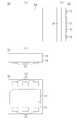
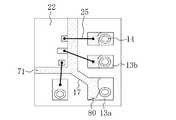
図1は本発明の第1の実施の形態にかかる半導体素子実装用基板10の構成を示す図であり、図1(a)は半導体素子実装用基板10の平面図であり、図1(b)は図1(a)に示すIB−IB線に沿って切断した断面図である。(First embodiment)
FIG. 1 is a diagram showing a configuration of a semiconductor
まず、半導体素子実装用基板10の構成を示す。 First, the configuration of the semiconductor
半導体素子実装用基板10は、ICチップ(図1には不図示)21,22を実装するための基板であり、図1に示すように、基板本体11と、設置部と、ダイパターン12,12と、複数の第1端子部13,13,…と、複数の貫通導体部14,14,…と、複数の第2端子部15,15,…と、絶縁性被膜18とを備えている。 The semiconductor
基板本体11は、絶縁性部材からなり、例えば、ガラス繊維及びケブラー(商標登録)等の有機化合物からなる繊維に、エポキシ樹脂、フェノール樹脂またはポリイミド樹脂等を含浸して硬化させた基板や、BTレジンからなる基板等の種々の樹脂基板を用いることができる。なお、本実施の形態では、基板本体11として、BTレジンからなる基板を用いる場合を例として説明する。また、基板本体11は、ICチップ21,22を実装するための実装面11aを有している。 The
設置部は、ICチップ21,22が設置される部位であり、実装面11aの中央部分に設けられており、具体的には、図1(a)に示すように、互いに離隔されて2つ設けられている。 The installation part is a part where the IC chips 21 and 22 are installed, and is provided in the central portion of the mounting
なお、設置部は、2つのICチップ21,22を設置することができるように2つ設けられているが、1つの設置部に2つのICチップ21,22を設置することもできる。そのため、設置部の個数は、設置するICチップの個数に制限されることなく選択できる。 In addition, although two installation parts are provided so that two
ダイパターン12,12は、それぞれ、設置部に設けられた銅箔等であり、ICチップ21,22と電気的に接続されている。すなわち、ICチップ21,22は、後述のように、ダイパターン12,12の上に設置される。 The
各貫通導体部14は、絶縁性被膜18よりも外側に、基板本体11の厚み方向に対して貫通して設けられており、互いに等間隔に設けられている。 The respective through
第1端子部13,13,…は、接地用第1端子部13a,13a,…と、電気的接続用第1端子部13b,13b,とで構成されており、各々、貫通導体部14,14,…から実装面11aの周縁部分へ向かって延びて設けられており、設置部(詳細には、設置部の中心)に対して放射状に配置されている。このように、第1端子部13,13,…は、各々、貫通導体部14,14,…よりも外側に配置されているため、熱などに起因して、ダイパターン12に設置したICチップ21,22がダイパターン12から剥離してしまった場合であっても、その剥離は貫通導体部14,14,…で止まる。 The first
接地用第1端子部13a,13a,…は、各々、ICチップ21,22を接地するための端子部であり、導体配線部17,17,…を介してダイパターン12と電気的に接続されている。すなわち、接地用第1端子部13a,13a,…は、各々、導体配線部17,17,…及びダイパターン12を介して、ダイパターン12に設置されるICチップ21,22に電気的に接続されて、ICチップ21,22を接地する。 The first
電気的接続用第1端子部13b,13b,…は、各々、ICチップ21,22に対して起動電力を供給するための端子部であり、後述のワイヤリード25,25,…を介して、ICチップ21,22の電極端子23,23,…と電気的に接続される。 The first
各第2端子部15は、外部電圧が印加される端子部であり、実装面11aとは反対側の面に設けられており、各貫通導体部14に接続されている。すなわち、第2端子部15,15,…は、各々、貫通導体部14,14,…、電気的接続用第1端子部13b,13b,…及びワイヤリード25,25,…を介して、ダイパターン12に設置されるICチップ21,22の電極端子23,23,…に電気的に接続されて、ICチップ21,22に起動電力を供給する。 Each second
絶縁性被膜18は、感光性樹脂材料からなり、ダイパターン12から貫通導体部14,14,…の手前まで延びて設けられている。この絶縁性被膜18は、フォトリソグラフィプロセスとエッチングプロセスとを用いて設けられている。このように、絶縁性被膜18は、ダイパターン12とダイパターン12を囲むダイパターン周囲とに設けられている。そのため、この半導体素子実装用基板10にICチップ21,22を実装させて樹脂封止型半導体装置とする場合には、封止樹脂26が絶縁性被膜18に接着され、その結果、ICチップ21,22の剥離を防止することができる。また、ダイパターン12に絶縁性被膜18が設けられているため、ダイパターンに絶縁性被膜が設けられていない場合に比べて、設置するICチップ21,22をダイパターン12に強固に固定することができる。 The insulating
ダイパターン12に設けられている絶縁性被膜18の部分には、孔16,16,…が設けられている。孔16,16,…は、各々絶縁性被膜18の膜厚方向に貫通しており、孔16,16,…が設けられた結果、ダイパターン12の一部が露出している。このように、孔16,16,…が設けられているため、絶縁性被膜18における応力の低減と絶縁性被膜18中の吸湿量の低減とを図ることができる。また、ダイパターン12にICチップ21,22を設置した場合には、後述の導電性接着剤24を介して、そのICチップ21,22とダイパターン12とを電気的に導通させることができる。 In the portion of the insulating
なお、図示していないが、絶縁性被膜18が設けられていないダイパターン12の部分、各第1端子部13、各貫通導体部14、各第2端子部15及び導体配線部17の上には、金薄膜(金膜)が設けられている。この金薄膜は、銅パターン上にニッケルメッキを行い、そのニッケルメッキの上に金メッキを行うことにより得られる。これにより、金薄膜が設けられた箇所における腐食を防止できる。また、後述のワイヤボンディングにおいて、ワイヤリード25,25,…を第1端子部13,13,…にそれぞれ強固に接着させることができる。 Although not shown, on the portion of the
次に、半導体素子実装用基板10の製造方法を示す。 Next, a method for manufacturing the semiconductor
まず、BTレジンからなる基板本体11の表面に、例えば銅箔を貼り付け、フォトリソグラフィプロセスとエッチングプロセスとを用いて所定のパターン形状に加工する。 First, for example, a copper foil is attached to the surface of the
具体的には、まず、例えば、厚みが約0.2mmのBTレジンからなる基板本体11の両面に、厚みが約18μmの銅箔を貼り付け、基板本体11に貫通孔の穴あけ加工を行う。次に、両面銅貼りされた樹脂基板11の表面に無電解銅メッキおよび電解銅メッキにより銅メッキ層(図示せず)を形成する。このとき、銅メッキ層は、貫通孔の内面にも設けられる。そして、フォトリソグラフィプロセスとエッチングプロセスとを行うことにより、図1に示すように、ダイパターン12、第1端子部13,13,…、貫通導体14,14,…、第2端子部15,15,…及び導体配線部17,17,…を設けることができる。 Specifically, first, for example, a copper foil having a thickness of about 18 μm is attached to both surfaces of a
次に、例えばメッキレジストフィルムをラミネートし、フォトリソグラフィプロセスとエッチングプロセスとを行うことにより、図1に示すように、絶縁性被膜18を設ける。具体的には、絶縁性被膜18を、ダイパターン12から貫通導体部14,14,…の手前まで延びて設ける。 Next, an insulating
なお、絶縁性被膜18は、このようなメッキレジストフィルムを用いて設けるだけでなく、例えば現像型液状ソルダーレジスト等の液状タイプを用いて設けてもよく、または、非感光性の熱硬化型ソルダーレジスト(ポリイミド樹脂系またはエポキシ樹脂系のいずれでもよい)、紫外線硬化型アクリレート系樹脂あるいは接着剤付ポリイミドテープ等を用いて設けてもよい。 The insulating
また、孔16,16,…は、ダイパターン12に設けられた絶縁性被膜18の部分に形成されているとしたが、ダイパターン周囲に設けられた絶縁性被膜18の部分にも形成されていてもよい。孔16,16,…を形成することにより、絶縁性被膜18における応力を低減することができ、基板本体11の反りの減少だけでなく、ICチップ21,22の剥離を抑制できる。さらに、孔16の個数は、図1(a)に記載の個数に限定されない。 In addition, although the
半導体素子実装用基板10が奏する効果を以下にまとめる。 The effects produced by the semiconductor
上述のように、ダイパターン12に設置されたICチップ21,22がダイパターン12から剥離してしまっても、その剥離は、貫通導体部14,14,…で止まり、第1端子部13,13,…にまで進行することを防止できる。その結果、第1端子部13,13,…及び導体配線部17,17,…における脱線を防止できる。さらに、ワイヤリード25,25,…を用いて、電気的接続用第1端子部13b,13b,…とICチップ21,22の電極端子23,23,…とをそれぞれ電気的に接続した場合には、そのワイヤリード25,25,…が電気的接続用第1端子部13b,13b,…やICチップ21,22の電極端子23,23,…からはずれることを防止できる。よって、この半導体素子実装用基板10を用いて樹脂封止型半導体装置をつくれば、使用中等にワイヤリード25,25,…が断線しにくい樹脂封止型半導体装置を提供でき、従来の半導体素子実装用基板を用いて製造された樹脂封止型半導体装置に比べて信頼性の高い半導体装置を提供できる。 As described above, even if the IC chips 21 and 22 installed on the
また、絶縁性被膜18がダイパターン周囲に設けられているため、ICチップ21,22がダイパターン12から剥離してしまうことを防止することができる。 Further, since the insulating
また、孔16,16,…が形成されているため、絶縁性被膜18における応力を低減することができ、その結果、基板本体11の反りを防止できる。よって、ダイパターン12に設置されたICチップ21,22がダイパターン12から剥離されることを防止できる。 Moreover, since the
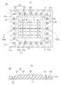
図2は、半導体素子実装用基板10を用いて半導体装置20を構成した場合の図であり、図2(a)は、半導体装置20の平面図であり、図2(b)は、図2(a)に示すIIB−IIB線に沿って切断した断面図である。なお、図2(a)では、図面をわかりやすくするために封止樹脂26を除去した状態を示している。 FIG. 2 is a diagram in the case where the
まず、半導体装置20の構成を示す。 First, the configuration of the
半導体装置20は、図2に示すように、ICチップ21,22と、上記の半導体素子実装用基板10と、ICチップ21,22の電極端子23,23,…と半導体素子実装用基板10の電気的接続用第1端子部13b,13b,…とをそれぞれ接続するワイヤリード25,25,…と、基板本体11の実装面11aにICチップ21,22及び各ワイヤリード25を埋設する封止樹脂26とを備えている。 As shown in FIG. 2, the
ICチップ21,22は、導電性接着剤24を介して、絶縁性被膜18及び各孔16により露出されているダイパターン12に接着されている。 The IC chips 21 and 22 are bonded to the
次に、半導体装置20の作製方法を示す。 Next, a method for manufacturing the
まず、図1に示す半導体素子実装用基板10のダイパターン12に対応する位置に、ICチップ21,22をそれぞれ位置合せして、例えば銀フィラーを添加したエポキシ系の導電性接着剤24を介して、絶縁性被膜18及び各孔16により露出されているダイパターン12に接着する。 First, the IC chips 21 and 22 are respectively aligned with the positions corresponding to the
次に、ワイヤリード25,25,…を用いてICチップ21,22の電極端子23,23,…と電気的接続用第1端子部13b,13b,…とをそれぞれ接続する。なお、ワイヤリード25としては、金線を用いることが好ましい。これにより、半導体素子実装用基板10とICチップ21,22との電気的接続が完了するので、第2端子部15,15,…に外部電圧を印加して、半導体装置20の電気的検査を行う。 Next, the
続いて、熱硬化性樹脂、例えばフィラーにシリカを使用したエポキシ系樹脂等の封止樹脂材料を用いて、ICチップ21,22及びワイヤリード25,25,…を埋設するように樹脂封止する。このとき、各貫通導体部14の開口にも封止樹脂26が入り込むので、半導体素子実装用基板10と封止樹脂26との接着性をより強固にすることができる。これにより、半導体装置20を作製することができる。 Subsequently, using a thermosetting resin, for example, a sealing resin material such as an epoxy resin using silica as a filler, resin sealing is performed so as to embed the IC chips 21, 22 and the wire leads 25, 25,. . At this time, since the sealing
半導体装置20は、上述の半導体素子実装用基板10を備えているために、半導体素子実装用基板10が奏する効果と略同一の効果を奏する。すなわち、一部でICチップ21,22の剥離が発生しても、その剥離の進行は、貫通導体部14や絶縁性被膜と封止樹脂との接着箇所により遮られる。その結果、ワイヤリード25,25,…、第1端子部13,13,…及び導体配線部17,17等での断線不良を防止でき、高信頼性の半導体装置20を実現できる。 Since the
また、孔16,16,…が設けられているため、絶縁性被膜18における応力の低減と絶縁性被膜18中の吸湿量の低減を図ることができる。そのため、半田リフロー工程や熱サイクル等によりICチップ21,22の剥離が生じ難くなる。 Further, since the
また、ダイパターン12に絶縁性被膜18が設けられているために、導電性接着剤を介して金薄膜だけが形成されたダイパターンにICチップを接着する場合に比べて、その接着力を大きくすることができる。 Further, since the insulating
続いて、半田耐熱試験を行って、半導体装置20の効果を検証した結果を示す。具体的には、図2に示す半導体装置20と図9に示す従来の半導体装置70とを用いて、はんだ耐熱試験を行った。 Subsequently, a result of verifying the effect of the
ここで、図9を用いて、従来の半導体装置70の構成を示す。図9(a)は、ICチップとしてシリコン半導体チップとガリウム砒素半導体チップとを用いて、半導体装置として電力増幅回路モジュールを作製した例を示す上面図であり、図9(b)は、IVB−IVB線に沿った断面図である。従来の半導体装置70は、半導体装置20と略同一の構成を示し、ICチップ21,22と、半導体素子実装用基板75と、ICチップ21,22の電極端子23,23,…と基板本体72の電気的接続用第1端子部13b,13b,…とをそれぞれ接続するワイヤリード25,25,…と、基板本体72の実装面にICチップ21,22及びワイヤリード25,25,…を埋設するように設けた封止樹脂26とを備えている。 Here, the configuration of a
半導体素子実装用基板75について簡単に示すと、基板本体72の実装面の中央部分には、ダイパターン71が設けられており、ダイパターン71よりも実装面の周縁部分には、複数の貫通導体部14,14,…が基板厚み方向に貫通している。また、第1端子部13,13,…は、各々、貫通導体部14,14,…からダイパターン71へ向かって延びて設けられており、第2端子部15,15,…は、各々、実装面とは反対側の面に設けられ、貫通導体部14,14,…に接続されている。すなわち、半導体素子実装用基板75は、絶縁性被膜が設けられていない点及び各第1端子部13が貫通導体部から実装面に反って延びる方向以外の点を除いては、半導体素子実装用基板10と略同一の構成である。 Briefly showing the semiconductor
では、本実施の形態におけるはんだ耐熱試験の手順を示す。はんだ耐熱試験では、まず、100〜130℃の温度で10〜20時間、ベーキングを行った。次に、85℃、65%RHで10〜24時間、吸湿を行った。続いて、250〜270℃の温度で10秒、リフロー加熱を行い、その後、85℃、65%RHで10〜24時間で吸湿を行った。そして、250〜270℃で10秒、リフロー加熱を行った。その後、非破壊で観察できる超音波映像装置SAT(Scanning Acoustic Tomograph)を用いて、封止樹脂26の剥離具合を調べた。具体的には、封止樹脂26が半導体素子実装用基板10の接地用第1端子部13a及び電気的接続用第1端子部13bから剥離していないか否か、また、封止樹脂26が半導体素子実装用基板75の接地用第1端子部13a及び電気的接続用第1端子部13bから剥離していないか否かを観察した。観察結果を表1に示す。 Then, the procedure of the solder heat test in this Embodiment is shown. In the solder heat resistance test, first, baking was performed at a temperature of 100 to 130 ° C. for 10 to 20 hours. Next, moisture absorption was performed at 85 ° C. and 65% RH for 10 to 24 hours. Subsequently, reflow heating was performed at a temperature of 250 to 270 ° C. for 10 seconds, and then moisture was absorbed at 85 ° C. and 65% RH for 10 to 24 hours. And reflow heating was performed at 250-270 degreeC for 10 second. Thereafter, the peeling state of the sealing

表1に示すように、従来の半導体装置70では、封止樹脂が剥離された箇所は、試験数12に対して、接地用第1端子部13aでも電気的接続用第1端子部13bでも全て観察された。 As shown in Table 1, in the
図10には、図9に示した従来の半導体装置70において、はんだ耐熱試験を行った場合の剥離発生箇所を模式的に示す。図10に示す結果から、剥離の進行について、次のようなことがいえる。すなわち、剥離は、ICチップ22直下のダイパターン71から始まって、導体配線部17へ進行し、更には、接地用第1端子部13aまで進行する。また同時に、ダイパターン71近傍の電気的接続用第1端子部13bにおいても、剥離が発生する。 FIG. 10 schematically shows a part where peeling occurs when a solder heat resistance test is performed in the
一方、半導体装置20では、表1に示すように、封止樹脂が剥離された箇所は、試験数12に対して、接地用第1端子部13aでは1箇所、電気的接続用第1端子部13bでは0箇所であった。この試験結果は、上述のように、各第1端子部13が各貫通導体部14よりも実装面の周縁部分に設けられているために、上記の剥離が絶縁性被膜18と封止樹脂26との接着箇所または各貫通導体部14により進行を抑制される結果、各第1端子部13にまで進行しないためである、と考えられる。また、ダイパターン周囲に設けられた絶縁性被膜と封止樹脂とが接着するため、上記剥離の発生を抑制することができるためである、と考えられる。よって、半導体装置20は、機械的強度の劣化や電気特性の劣化、またはワイヤリード25,25,…の断線等の発生を抑制することができる。 On the other hand, as shown in Table 1, in the
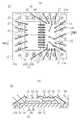
図3は、ICチップとしてシリコン半導体チップとガリウム砒素半導体チップとを用いて、半導体装置として電力増幅回路モジュール30を作製した例を示す外形図である。図3(a)は、電力増幅回路モジュール30の上面図であり、図3(b)は、電力増幅回路モジュール30の右側面図であり、図3(c)は、電力増幅回路モジュールの30正面側面図であり、図3(d)は、電力増幅回路モジュール30の下面図である。電力増幅回路モジュール30は、上記の半導体素子実装用基板10と略同一の内部構成を有する半導体素子実装用基板31を備えているが、この半導体素子実装用基板31では、図3(d)に示すように、第2端子部32,32,…が基板本体の裏面の2辺に沿って設けられており、基板本体の裏面の中央部分に接地用第1端子部33が設けられていることを特徴とする。 FIG. 3 is an outline view showing an example in which a power
基板本体はBTレジンからなり、封止樹脂34はエポキシ樹脂であり、電気的接続用第1端子部(図示せず)、ダイパターン(図示せず)、第2端子部32,32,…及び接地用第1端子部33には、各々、それらの表面に無電解金メッキが形成されている。電力増幅回路モジュール30の外形寸法は、4mm×4mm×1.2mmである。このような電力増幅回路モジュール30を作製して半田リフロー耐熱性を測定した結果、不良発生が0個であった。また、このような電力増幅回路モジュール30を用いて熱サイクル試験を行った結果、このような電力増幅回路モジュールが良好な信頼性を有することを確認できた。なお、このような電力増幅回路モジュール30は、携帯電話の電力増幅回路等に用いることができる。 The substrate body is made of BT resin, and the sealing
(第2の実施の形態)
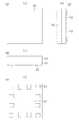
図4は、第2の実施の形態にかかる半導体素子実装用基板35の構成を示す図で、図4(a)は、半導体素子実装用基板35の平面図であり、図4(b)は、図4(a)に示すIVB−IVB線に沿った断面図である。(Second Embodiment)
FIG. 4 is a diagram showing a configuration of the semiconductor
本実施の形態の半導体素子実装用基板35は、上記第1の実施の形態の半導体素子実装用基板10と比較して、絶縁性被膜36の形状が異なることが特徴である。 The semiconductor
すなわち、本実施の形態では、絶縁性被膜36はダイパターン周囲にのみ設けられている。これにより、半導体素子実装用基板35は、上記第1の実施の形態の半導体素子実装用基板10と略同一の効果を奏するとともに、絶縁性被膜36がダイパターン12には設けられていないため、上記実施の形態1の半導体素子実装用基板10よりも、半導体装置の薄型化を図ることができ、また、ダイパターン12に設置するICチップ21,22とダイパターン12との電気的導通を容易に行うことができる。その上、絶縁性被膜36の表面積が小さくなるので吸湿量も少なくなり、半田リフロー等において、吸湿成分がガス化してICチップ21,22の剥離の助長を抑制することができる。以上より、半導体装置の製造時に厳密な湿度管理等をしなくても、製造歩留まりが高く、かつ高信頼性の半導体装置を実現できる。 That is, in the present embodiment, the insulating
なお、この絶縁性被膜36は、感光性樹脂材料からなり、フォトリソグラフィプロセスとエッチングプロセスとにより加工されている。また、ダイパターン12、各第1端子部13、各貫通導体部14、各第2端子部15及び各導体配線部17には、金薄膜が形成されている。 The insulating
図5は、この半導体素子実装用基板35を用いて作製された半導体装置40の構成を示す図であり、図5(a)は、半導体装置40の平面図であり、図5(b)は、図5(a)に示すVB−VB線に沿った断面図である。 FIG. 5 is a diagram showing a configuration of a
本実施の形態の半導体装置40は、上記第1の実施の形態の半導体装置20と比較して、半導体素子実装用基板35の構成が異なることが特徴である。そのため、半導体装置40は、半導体素子実装用基板35が奏する効果と略同一の効果を奏する。すなわち、絶縁性被膜36がダイパターン周囲に設けられている。そのため、絶縁性被膜36と封止樹脂26との接着性が大きく、かつ封止樹脂26が貫通導体部14,14,…中にも入り込むために、ICチップ21,22の一部がダイパターン12から剥離してしまっても、その剥離が貫通導体部14,14,…の領域へ進行してしまうことを防止できる。このため、第1端子部13,13,…やワイヤリード25,25,…の断線等の不良発生を防止できる。 The
さらに、導電性接着剤24を用いて、ダイパターン12上にICチップ21,22を直接接着するため、ICチップ21,22とダイパターン12との電気的導通をとりやすい。また、ダイパターン12に絶縁性被膜36を設けていないため、半導体装置40の薄型化を図ることができる。さらに、絶縁性被膜36の形成面積が小さくなるので吸湿量も少なくなり、半田リフロー等において、吸湿成分がガス化して剥離を助長することも抑制しやすい。これらにより、製造時に厳密な湿度管理等をしなくても、製造歩留まりが高く、かつ高信頼性の半導体装置40を実現できる。 Further, since the IC chips 21 and 22 are directly bonded onto the
(第3の実施の形態)
図6は、第3の実施の形態にかかる半導体素子実装用基板45の構成を示す図であり、図6(a)は、半導体素子実装用基板45の平面図であり、図6(b)は、図6(a)に示すVIB−VIB線に沿った断面図である。(Third embodiment)
FIG. 6 is a diagram showing a configuration of a semiconductor
本実施の形態の半導体素子実装用基板45は、上記第1の実施の形態の半導体素子実装用基板10と比較して、絶縁性被膜46の形状が異なること、およびダイパターン49の外形がICチップ21,22の外形よりそれぞれ小さいことが特徴である。 The semiconductor
すなわち、本実施の形態では、絶縁性被膜46は、ダイパターン周囲にのみ設けられた第1の絶縁性被膜47と、ダイパターン49に設けられた複数の第2の絶縁性被膜48,48,…とで構成されている。第2の絶縁性被膜48,48,…は、各々、互いに分離してアレイ状に配置されている。第1の絶縁性被膜47及び第2の絶縁性被膜48,48,…は、各々、感光性樹脂材料からなり、フォトリソグラフィプロセスとエッチングプロセスとを用いて加工されている。 That is, in the present embodiment, the insulating
また、ダイパターン49の外形は、ICチップ21,22の外形より小さい。 Further, the outer shape of the
また、第2の絶縁性被膜48,48,…が設けられていないダイパターン49、第1端子部13,13,…、貫通導体部14,14,…、第2端子部15,15,…及び導体配線部17,17,…には、金薄膜が形成されている。 In addition, the
このような半導体素子実装用基板45は、上記実施の形態1の半導体素子実装用基板10と略同一の効果を奏し、基板本体11の厚みを薄くしても反りが生じ難く、かつICチップ21,22を実装しても剥離等が生じ難い。 Such a semiconductor
ダイパターン49には第2の絶縁性被膜48,48,…が設けられているため、第2の絶縁性被膜が設けられていないダイパターンに金薄膜を形成してICチップを設置する場合に比べて、ICチップ21,22をダイパターン49に強く接着させることができる。 Since the
また、第2の絶縁性被膜48,48,…が互いに分離されて設けられているため、絶縁性被膜46は、全体として、応力を低減することができる。また、ダイパターン49の外形寸法は、ICチップ21,22の外形寸法よりも小さいため、ダイパターン49で発生する応力も低減できる。この結果、ICチップ21,22を実装し、封止樹脂26を用いて封止しても、ICチップ21,22の剥離等の不良発生を確実に防止できる。したがって、半田リフロー実装や熱サイクルを受けても、ワイヤリード25,25,…や第1端子部13,13,…あるいは導体配線部17,17,…等の断線不良を防止できる。 Further, since the second insulating
図7は、半導体素子実装用基板45を用いて作製された半導体装置55の構成を示す図であり、図7(a)は、半導体装置55の平面図であり、図7(b)は、図7(a)に示すVIIB−VIIB線に沿った断面図である。 FIG. 7 is a diagram illustrating a configuration of a
本実施の形態の半導体装置55は、上記第1の実施の形態の半導体装置20と比較して、半導体素子実装用基板45の構成が異なることが特徴である。そのため、半導体装置55は、半導体素子実装用基板45が奏する効果と略同一の効果を奏する。 The
以下、本実施の形態の半導体装置55の作製方法を簡単に説明する。 Hereinafter, a method for manufacturing the
まず、図6に示す半導体素子実装用基板45のダイパターン49に、ICチップ21,22をそれぞれ位置合せして、例えば銀フィラーを添加したエポキシ系の導電性接着剤24を介して、第2の絶縁性被膜48,48,…及び第2の絶縁性被膜48,48が設けられていないダイパターン49の部分に、それぞれ接着する。 First, the IC chips 21 and 22 are respectively aligned with the
次に、ワイヤリード25,25を用いて、ICチップ21,22の電極端子23,23,…と電気的接続用第1端子部13b,13b,…とをワイヤーボンディングして接続する。なお、ワイヤリード25としては、金線を用いることが好ましい。これにより、半導体素子実装用基板45とICチップ21,22との電気的接続が完了するので、第2端子部15,15,…に外部電圧を印加して、半導体装置55の電気的検査を行う。 Next, using the wire leads 25, 25, the
続いて、熱硬化性樹脂、例えばフィラーにシリカを使用したエポキシ系樹脂等の封止樹脂材料を用いて、ICチップ21,22およびワイヤリード25,25,…を埋設するように樹脂封止する。このとき、各貫通導体14の開口にも封止樹脂26が入り込むので、半導体素子実装用基板45と封止樹脂26との接着性をより強固にすることができる。これにより、半導体装置55を作製することができる。 Subsequently, using a thermosetting resin, for example, a sealing resin material such as an epoxy resin using silica as a filler, resin sealing is performed so as to embed the IC chips 21, 22 and the wire leads 25, 25,. . At this time, since the sealing
このような構成からなる本実施の形態の半導体装置55では、上述の半導体素子実装用基板45を備えているため、半導体素子実装用基板45と略同一の効果を奏する。 Since the
すなわち、ICチップ21,22は、第2の絶縁性被膜48,48,…で主として接着強度を保持しており、導電性接着剤24を用いて金薄膜のみが形成されたダイパターンに比べて、強く接着される。 That is, the IC chips 21 and 22 mainly maintain the adhesive strength by the second insulating
第2の絶縁性被膜48,48,…が互いに分離されて設けられているため、絶縁性被膜46は、全体として、応力を低減することができる。また、ダイパターン49の外形寸法は、ICチップ21,22の外形寸法よりも小さいため、ダイパターン49で発生する応力も低減できる。この結果、ICチップ21,22を実装し、封止樹脂26を用いて封止しても、ICチップ21,22の剥離等の不良発生を確実に防止できる。したがって、半田リフロー実装や熱サイクルを受けても、ワイヤリード25,25,…や第1端子部13,13,…あるいは導体配線部17,17,…等の断線不良を防止できる。 Since the second insulating
図8は、ICチップとしてシリコン半導体チップとガリウム砒素半導体チップとを用いて、半導体装置として電力増幅回路モジュール60を作製した例を示す外形図であり、図8(a)は、電力増幅回路モジュール60の上面図であり、図8(b)は、電力増幅回路モジュール60の右側面図であり、図8(c)は、電力増幅回路モジュール60の正面側面図であり、図8(d)は、電力増幅回路モジュール60の下面図である。電力増幅回路モジュール60は、上記の半導体素子実装用基板45と略同一の内部構成を有する半導体素子実装用基板61を備えているが、半導体素子実装用基板61では、図8(d)に示すように、第2端子部62,62,…の端子数が異なり、また、貫通導体部(図示せず)及び第1端子部(図示せず)の個数も同様に異なる基板本体を用いている。 FIG. 8 is an outline view showing an example in which a power
基板本体はBTレジンからなり、封止樹脂63はエポキシ樹脂を用いている。また、第1端子部(図示せず)、ダイパターン(図示せず)及び第2端子部62等は、表面に無電解金メッキが形成されている。電力増幅回路モジュール60の外形寸法は、2mm×2mm×0.6mmである。このような電力増幅回路モジュール60を作製して半田リフロー耐熱性を測定した結果、不良発生が0個であった。また、熱サイクル試験を行った結果、良好な信頼性を有することを確認できた。この電力増幅回路モジュール60は携帯電話の電力増幅回路に用いられる。 The substrate body is made of BT resin, and the sealing
(その他の実施形態)
上記第1の実施の形態から上記第3の実施の形態までにおいては、半導体素子実装用基板のダイパターンの下部に配線パターンや貫通孔を形成しない構成について説明したが、ダイパターンの下部に貫通孔を形成してもよい。(Other embodiments)
From the first embodiment to the third embodiment, the configuration in which the wiring pattern and the through hole are not formed in the lower part of the die pattern of the semiconductor element mounting substrate has been described. A hole may be formed.
また、半導体素子実装用基板は両面配線構成について説明したが、本発明はこれに限定されず、多層配線構成であってもよい。 Moreover, although the board | substrate for semiconductor element mounting demonstrated the double-sided wiring structure, this invention is not limited to this, A multilayer wiring structure may be sufficient.
また、実装面あるいは第2端子部を形成する面に、配線パターンがさらに形成されていてもよい。 A wiring pattern may be further formed on the mounting surface or the surface on which the second terminal portion is formed.
本発明に係る半導体素子実装用基板および半導体装置は、ICチップの剥離や封止樹脂の膨れ等により生じる断線等の不良発生を防止でき、高信頼性で、かつ安価な半導体装置を実現でき、種々の電子機器、特に携帯用電子機器分野に有用である。 The semiconductor element mounting substrate and the semiconductor device according to the present invention can prevent occurrence of defects such as disconnection caused by peeling of the IC chip or swelling of the sealing resin, and can realize a highly reliable and inexpensive semiconductor device. It is useful in various electronic devices, particularly in the field of portable electronic devices.
10,31,35,45,61,75 半導体素子実装用基板
11,72 基板本体
11a 実装面
12,49,71 ダイパターン
13 第1端子部
13a 接地用第1端子部
14 貫通導体部
15,32,62 第2端子部
16 孔
18,36,46 絶縁性被膜
20,40,55,70 半導体装置
21,22 ICチップ(半導体素子)
26,34,63 封止樹脂
30,60 電力増幅回路モジュール
47 第1の絶縁性被膜(絶縁性被膜)
48 第2の絶縁性被膜(絶縁性被膜)10, 31, 35, 45, 61, 75 Semiconductor
26, 34, 63 Sealing
48 Second insulating coating (insulating coating)
Claims (28)
Translated fromJapanese前記実装面に設けられ、前記半導体素子を設置する設置部と、
前記設置部よりも外側に、前記基板本体を厚み方向に貫通して設けられた複数の貫通導体部と、
前記貫通導体部から前記実装面の周縁へ向かって該実装面上に各々延びて設けられ、前記半導体素子と電気的に接続される複数の第1端子部と、
前記実装面とは反対側の面に設けられ、各々、前記貫通導体部に接続されて前記第1端子部と電気的に接続された複数の第2端子部と
を備えていることを特徴とする半導体素子実装用基板。A substrate body having a mounting surface on which a semiconductor element is mounted;
An installation part provided on the mounting surface and installing the semiconductor element;
A plurality of through conductor portions provided outside the installation portion and penetrating the substrate body in the thickness direction;
A plurality of first terminal portions provided extending from the through conductor portion toward the periphery of the mounting surface on the mounting surface and electrically connected to the semiconductor element;
A plurality of second terminal portions provided on a surface opposite to the mounting surface, each connected to the through conductor portion and electrically connected to the first terminal portion; A semiconductor device mounting substrate.
前記複数の第1端子部のうちの少なくとも一つの該第1端子部は、前記ダイパターンを接地するための接地用第1端子部であり、
前記接地用第1端子部と前記ダイパターンとを電気的に接続する導体配線部を有していることを特徴とする請求項1に記載の半導体素子実装用基板。The installation part is provided with a die pattern electrically connected to the semiconductor element,
At least one first terminal portion of the plurality of first terminal portions is a grounding first terminal portion for grounding the die pattern;
2. The semiconductor element mounting substrate according to claim 1, further comprising a conductor wiring portion that electrically connects the first grounding terminal portion and the die pattern.
前記ダイパターンに設けられた絶縁性被膜には、少なくとも一つの孔が膜厚方向に該ダイパターンにまで貫通していることを特徴とする請求項5に記載の半導体素子実装用基板。The insulating coating extends from the die pattern to the periphery of the die pattern,
6. The semiconductor element mounting substrate according to claim 5, wherein the insulating film provided on the die pattern has at least one hole penetrating through the die pattern in a film thickness direction.
前記半導体素子実装用基板は、
前記半導体素子が実装される実装面を有する基板本体と、
前記実装面に設けられ、前記半導体素子を設置する設置部と、
前記設置部よりも外側に、前記基板本体を厚み方向に貫通して設けられた複数の貫通 導体部と、
前記貫通導体部から前記実装面の周縁へ向かって該実装面上に各々延びて設けられ、 前記半導体素子と電気的に接続される複数の第1端子部と、
前記実装面とは反対側の面に設けられ、各々、前記貫通導体部に接続されて前記第1 端子部と電気的に接続された複数の第2端子部と
を備えていることを特徴とする半導体装置。A semiconductor device in which a semiconductor element is mounted on a semiconductor element mounting substrate,
The semiconductor element mounting substrate is:
A substrate body having a mounting surface on which the semiconductor element is mounted;
An installation part provided on the mounting surface and installing the semiconductor element;
A plurality of through conductor portions provided outside the installation portion and penetrating the substrate body in the thickness direction;
A plurality of first terminal portions, each extending from the through conductor portion toward the periphery of the mounting surface on the mounting surface, and electrically connected to the semiconductor element;
A plurality of second terminal portions provided on a surface opposite to the mounting surface, each connected to the through conductor portion and electrically connected to the first terminal portion; Semiconductor device.
前記複数の第1端子部のうちの少なくとも一つの該第1端子部は、前記ダイパターンを接地するための接地用第1端子部であり、
前記接地用第1端子部と前記ダイパターンとを電気的に接続する導体配線部を有していることを特徴とする請求項12に記載の半導体装置。The installation part is provided with a die pattern electrically connected to the semiconductor element,
At least one first terminal portion of the plurality of first terminal portions is a grounding first terminal portion for grounding the die pattern;
13. The semiconductor device according to claim 12, further comprising a conductor wiring portion that electrically connects the first grounding terminal portion and the die pattern.
前記封止樹脂は、前記絶縁性被膜に接着されていることを特徴とする請求項17に記載の半導体装置。A sealing resin for sealing the semiconductor element;
The semiconductor device according to claim 17, wherein the sealing resin is bonded to the insulating coating.
前記ダイパターンに設けられた絶縁性被膜には、少なくとも1つの孔が膜厚方向に該ダイパターンにまで貫通していることを特徴とする請求項17に記載の半導体装置。The insulating coating extends from the die pattern to the periphery of the die pattern,
18. The semiconductor device according to claim 17, wherein the insulating film provided on the die pattern has at least one hole penetrating through the die pattern in the film thickness direction.
An electronic apparatus comprising the semiconductor device according to claim 12.
Priority Applications (3)
| Application Number | Priority Date | Filing Date | Title |
|---|---|---|---|
| JP2006001586AJP2007184414A (en) | 2006-01-06 | 2006-01-06 | Semiconductor device mounting substrate, semiconductor device and electronic apparatus |
| CNA2006101492441ACN1996586A (en) | 2006-01-06 | 2006-11-21 | Semiconductor-element mounting substrate, semiconductor device, and electronic equipment |
| US11/607,001US7816777B2 (en) | 2006-01-06 | 2006-12-01 | Semiconductor-element mounting substrate, semiconductor device, and electronic equipment |
Applications Claiming Priority (1)
| Application Number | Priority Date | Filing Date | Title |
|---|---|---|---|
| JP2006001586AJP2007184414A (en) | 2006-01-06 | 2006-01-06 | Semiconductor device mounting substrate, semiconductor device and electronic apparatus |
Publications (1)
| Publication Number | Publication Date |
|---|---|
| JP2007184414Atrue JP2007184414A (en) | 2007-07-19 |
Family
ID=38232057
Family Applications (1)
| Application Number | Title | Priority Date | Filing Date |
|---|---|---|---|
| JP2006001586APendingJP2007184414A (en) | 2006-01-06 | 2006-01-06 | Semiconductor device mounting substrate, semiconductor device and electronic apparatus |
Country Status (3)
| Country | Link |
|---|---|
| US (1) | US7816777B2 (en) |
| JP (1) | JP2007184414A (en) |
| CN (1) | CN1996586A (en) |
Cited By (4)
| Publication number | Priority date | Publication date | Assignee | Title |
|---|---|---|---|---|
| JP2011124487A (en)* | 2009-12-14 | 2011-06-23 | Renesas Electronics Corp | Method of manufacturing semiconductor device |
| JP2013042136A (en)* | 2011-08-17 | 2013-02-28 | Samsung Electronics Co Ltd | Package laminate structure |
| JP2015115432A (en)* | 2013-12-11 | 2015-06-22 | ローム株式会社 | Semiconductor device |
| JP2018142746A (en)* | 2018-06-20 | 2018-09-13 | ローム株式会社 | Semiconductor device |
Families Citing this family (8)
| Publication number | Priority date | Publication date | Assignee | Title |
|---|---|---|---|---|
| TWI358797B (en)* | 2007-09-11 | 2012-02-21 | Advanced Semiconductor Eng | A wireless communication module with power amplifi |
| SG155096A1 (en) | 2008-03-03 | 2009-09-30 | Micron Technology Inc | Board-on-chip type substrates with conductive traces in multiple planes, semiconductor device packages including such substrates, and associated methods |
| US8138587B2 (en)* | 2008-09-30 | 2012-03-20 | Infineon Technologies Ag | Device including two mounting surfaces |
| JP5250524B2 (en)* | 2009-10-14 | 2013-07-31 | ルネサスエレクトロニクス株式会社 | Semiconductor device and manufacturing method thereof |
| JP6370652B2 (en)* | 2014-09-16 | 2018-08-08 | 東芝メモリ株式会社 | Semiconductor device |
| EP3088931B1 (en) | 2015-04-30 | 2024-09-04 | LG Innotek Co., Ltd. | Lens moving apparatus and camera module and optical device including the same |
| JP6806520B2 (en)* | 2016-10-17 | 2021-01-06 | ラピスセミコンダクタ株式会社 | How to design semiconductor devices and wiring boards |
| JP2022082887A (en)* | 2020-11-24 | 2022-06-03 | ルネサスエレクトロニクス株式会社 | Semiconductor devices and their manufacturing methods |
Citations (6)
| Publication number | Priority date | Publication date | Assignee | Title |
|---|---|---|---|---|
| JPH08316360A (en)* | 1995-05-18 | 1996-11-29 | Citizen Watch Co Ltd | Ic mounting structure |
| JPH0997860A (en)* | 1995-06-12 | 1997-04-08 | Citizen Watch Co Ltd | Semiconductor device |
| JPH10214912A (en)* | 1997-01-30 | 1998-08-11 | Sony Corp | Semiconductor device, its manufacture, and wiring board |
| JP2000133742A (en)* | 1998-10-23 | 2000-05-12 | Hitachi Ltd | Package substrate, semiconductor device using the same, and method of manufacturing the same |
| JP2002033347A (en)* | 2000-07-17 | 2002-01-31 | Rohm Co Ltd | Semiconductor device |
| JP2005093743A (en)* | 2003-09-18 | 2005-04-07 | Ibiden Co Ltd | Printed wiring board |
Family Cites Families (12)
| Publication number | Priority date | Publication date | Assignee | Title |
|---|---|---|---|---|
| US3978248A (en)* | 1970-12-18 | 1976-08-31 | Hitachi, Ltd. | Method for manufacturing composite sintered structure |
| US5173766A (en)* | 1990-06-25 | 1992-12-22 | Lsi Logic Corporation | Semiconductor device package and method of making such a package |
| US5216278A (en)* | 1990-12-04 | 1993-06-01 | Motorola, Inc. | Semiconductor device having a pad array carrier package |
| US5639989A (en)* | 1994-04-19 | 1997-06-17 | Motorola Inc. | Shielded electronic component assembly and method for making the same |
| JP3672885B2 (en) | 1994-08-15 | 2005-07-20 | シチズン時計株式会社 | Semiconductor device |
| US5767447A (en)* | 1995-12-05 | 1998-06-16 | Lucent Technologies Inc. | Electronic device package enclosed by pliant medium laterally confined by a plastic rim member |
| US5973337A (en)* | 1997-08-25 | 1999-10-26 | Motorola, Inc. | Ball grid device with optically transmissive coating |
| JP3784976B2 (en)* | 1998-12-22 | 2006-06-14 | ローム株式会社 | Semiconductor device |
| TW417220B (en)* | 1999-07-23 | 2001-01-01 | Advanced Semiconductor Eng | Packaging structure and method of semiconductor chip |
| EP1237189A1 (en)* | 2001-02-28 | 2002-09-04 | Motorola, Inc. | Arrangement and method for impedance matching |
| JP3897749B2 (en) | 2003-10-31 | 2007-03-28 | 沖電気工業株式会社 | Semiconductor device |
| JP2005340647A (en)* | 2004-05-28 | 2005-12-08 | Nec Compound Semiconductor Devices Ltd | Interposer substrate, semiconductor package, semiconductor device, and method for manufacturing them |
- 2006
- 2006-01-06JPJP2006001586Apatent/JP2007184414A/enactivePending
- 2006-11-21CNCNA2006101492441Apatent/CN1996586A/enactivePending
- 2006-12-01USUS11/607,001patent/US7816777B2/ennot_activeExpired - Fee Related
Patent Citations (6)
| Publication number | Priority date | Publication date | Assignee | Title |
|---|---|---|---|---|
| JPH08316360A (en)* | 1995-05-18 | 1996-11-29 | Citizen Watch Co Ltd | Ic mounting structure |
| JPH0997860A (en)* | 1995-06-12 | 1997-04-08 | Citizen Watch Co Ltd | Semiconductor device |
| JPH10214912A (en)* | 1997-01-30 | 1998-08-11 | Sony Corp | Semiconductor device, its manufacture, and wiring board |
| JP2000133742A (en)* | 1998-10-23 | 2000-05-12 | Hitachi Ltd | Package substrate, semiconductor device using the same, and method of manufacturing the same |
| JP2002033347A (en)* | 2000-07-17 | 2002-01-31 | Rohm Co Ltd | Semiconductor device |
| JP2005093743A (en)* | 2003-09-18 | 2005-04-07 | Ibiden Co Ltd | Printed wiring board |
Cited By (4)
| Publication number | Priority date | Publication date | Assignee | Title |
|---|---|---|---|---|
| JP2011124487A (en)* | 2009-12-14 | 2011-06-23 | Renesas Electronics Corp | Method of manufacturing semiconductor device |
| JP2013042136A (en)* | 2011-08-17 | 2013-02-28 | Samsung Electronics Co Ltd | Package laminate structure |
| JP2015115432A (en)* | 2013-12-11 | 2015-06-22 | ローム株式会社 | Semiconductor device |
| JP2018142746A (en)* | 2018-06-20 | 2018-09-13 | ローム株式会社 | Semiconductor device |
Also Published As
| Publication number | Publication date |
|---|---|
| US7816777B2 (en) | 2010-10-19 |
| US20070158855A1 (en) | 2007-07-12 |
| CN1996586A (en) | 2007-07-11 |
Similar Documents
| Publication | Publication Date | Title |
|---|---|---|
| JP2007184414A (en) | Semiconductor device mounting substrate, semiconductor device and electronic apparatus | |
| JP4058642B2 (en) | Semiconductor device | |
| US9760754B2 (en) | Printed circuit board assembly forming enhanced fingerprint module | |
| JP2003522401A (en) | Stacked integrated circuit package | |
| JP2010251395A (en) | Electronic device and method of manufacturing the same | |
| JP4876618B2 (en) | Semiconductor device and manufacturing method of semiconductor device | |
| JP4070470B2 (en) | Multilayer circuit board for semiconductor device, manufacturing method thereof, and semiconductor device | |
| JP5357239B2 (en) | WIRING BOARD, SEMICONDUCTOR DEVICE, AND WIRING BOARD MANUFACTURING METHOD | |
| TW201603665A (en) | Printed circuit board, method for manufacturing the same and package on package having the same | |
| JP4945682B2 (en) | Semiconductor memory device and manufacturing method thereof | |
| JP2005294443A (en) | Semiconductor device and its manufacturing method | |
| JP2009246174A (en) | Semiconductor module, method of manufacturing semiconductor module, and portable equipment | |
| CN1998076A (en) | Semiconductor device and semiconductor device producing substrate and production method for semiconductor device producing substrate | |
| JP5484694B2 (en) | Semiconductor module and portable device equipped with semiconductor module | |
| JP2009060144A (en) | Multi-layer substrate with built-in electronic part | |
| US20120225521A1 (en) | Board on chip package substrate and manufacturing method thereof | |
| JP2004128356A (en) | Semiconductor device | |
| JP2009038265A (en) | Semiconductor device substrate | |
| JPH0342860A (en) | Flexible printed wiring board | |
| JP3033541B2 (en) | TAB tape, semiconductor device, and method of manufacturing semiconductor device | |
| JPH06163737A (en) | Semiconductor device and its production | |
| JPH11111882A (en) | Wiring board for BGA type semiconductor device and BGA type semiconductor device | |
| US20090179326A1 (en) | Semiconductor device package | |
| KR101185854B1 (en) | Semiconductor package | |
| JP3818591B2 (en) | Electronic component with through-hole electrode and method for manufacturing the same |
Legal Events
| Date | Code | Title | Description |
|---|---|---|---|
| A621 | Written request for application examination | Free format text:JAPANESE INTERMEDIATE CODE: A621 Effective date:20080805 | |
| A977 | Report on retrieval | Free format text:JAPANESE INTERMEDIATE CODE: A971007 Effective date:20101025 | |
| A131 | Notification of reasons for refusal | Free format text:JAPANESE INTERMEDIATE CODE: A131 Effective date:20101214 | |
| A521 | Request for written amendment filed | Free format text:JAPANESE INTERMEDIATE CODE: A523 Effective date:20110210 | |
| A131 | Notification of reasons for refusal | Free format text:JAPANESE INTERMEDIATE CODE: A131 Effective date:20120110 | |
| A02 | Decision of refusal | Free format text:JAPANESE INTERMEDIATE CODE: A02 Effective date:20120508 |