JP2007179286A - Storage device and information processor - Google Patents
Storage device and information processorDownload PDFInfo
- Publication number
- JP2007179286A JP2007179286AJP2005376686AJP2005376686AJP2007179286AJP 2007179286 AJP2007179286 AJP 2007179286AJP 2005376686 AJP2005376686 AJP 2005376686AJP 2005376686 AJP2005376686 AJP 2005376686AJP 2007179286 AJP2007179286 AJP 2007179286A
- Authority
- JP
- Japan
- Prior art keywords
- file
- area
- storage device
- information
- stored
- Prior art date
- Legal status (The legal status is an assumption and is not a legal conclusion. Google has not performed a legal analysis and makes no representation as to the accuracy of the status listed.)
- Granted
Links
Images


Classifications
- G—PHYSICS
- G06—COMPUTING OR CALCULATING; COUNTING
- G06F—ELECTRIC DIGITAL DATA PROCESSING
- G06F3/00—Input arrangements for transferring data to be processed into a form capable of being handled by the computer; Output arrangements for transferring data from processing unit to output unit, e.g. interface arrangements
- G06F3/06—Digital input from, or digital output to, record carriers, e.g. RAID, emulated record carriers or networked record carriers
- G06F3/0601—Interfaces specially adapted for storage systems
- G06F3/0628—Interfaces specially adapted for storage systems making use of a particular technique
- G06F3/0638—Organizing or formatting or addressing of data
- G06F3/0643—Management of files
- G—PHYSICS
- G06—COMPUTING OR CALCULATING; COUNTING
- G06F—ELECTRIC DIGITAL DATA PROCESSING
- G06F3/00—Input arrangements for transferring data to be processed into a form capable of being handled by the computer; Output arrangements for transferring data from processing unit to output unit, e.g. interface arrangements
- G06F3/06—Digital input from, or digital output to, record carriers, e.g. RAID, emulated record carriers or networked record carriers
- G06F3/0601—Interfaces specially adapted for storage systems
- G06F3/0602—Interfaces specially adapted for storage systems specifically adapted to achieve a particular effect
- G06F3/0614—Improving the reliability of storage systems
- G06F3/0616—Improving the reliability of storage systems in relation to life time, e.g. increasing Mean Time Between Failures [MTBF]
- G—PHYSICS
- G06—COMPUTING OR CALCULATING; COUNTING
- G06F—ELECTRIC DIGITAL DATA PROCESSING
- G06F3/00—Input arrangements for transferring data to be processed into a form capable of being handled by the computer; Output arrangements for transferring data from processing unit to output unit, e.g. interface arrangements
- G06F3/06—Digital input from, or digital output to, record carriers, e.g. RAID, emulated record carriers or networked record carriers
- G06F3/0601—Interfaces specially adapted for storage systems
- G06F3/0668—Interfaces specially adapted for storage systems adopting a particular infrastructure
- G06F3/0671—In-line storage system
- G06F3/0673—Single storage device
- G06F3/0679—Non-volatile semiconductor memory device, e.g. flash memory, one time programmable memory [OTP]
- G—PHYSICS
- G11—INFORMATION STORAGE
- G11C—STATIC STORES
- G11C29/00—Checking stores for correct operation ; Subsequent repair; Testing stores during standby or offline operation
- G11C29/70—Masking faults in memories by using spares or by reconfiguring
- G11C29/76—Masking faults in memories by using spares or by reconfiguring using address translation or modifications
Landscapes
- Engineering & Computer Science (AREA)
- Theoretical Computer Science (AREA)
- Human Computer Interaction (AREA)
- Physics & Mathematics (AREA)
- General Engineering & Computer Science (AREA)
- General Physics & Mathematics (AREA)
- Information Retrieval, Db Structures And Fs Structures Therefor (AREA)
Abstract
Description
Translated fromJapanese本発明は、記憶装置に対するファイルの格納技術に関する。 The present invention relates to a file storage technique for a storage device.
メモリの大容量化に伴い、メモリの記憶領域の一部に不良領域が存在するメモリ(以降ノンパーフェクトメモリと呼ぶ。)が広く利用されている。 Along with an increase in memory capacity, a memory having a defective area in a part of a memory area (hereinafter referred to as a non-perfect memory) is widely used.
このようなメモリにおいては、一般的にページ単位で不良領域に対する代替処理が必要であり、その情報(代替ページ情報)は、メモリの記憶領域の一部に格納されている。ここで言う代替ページ情報とは、どのページに故障があって、どのページに差し替えるかの情報である。 Such a memory generally requires a substitute process for a defective area in units of pages, and the information (substitute page information) is stored in a part of the memory area of the memory. The alternative page information mentioned here is information indicating which page has a failure and which page is replaced.
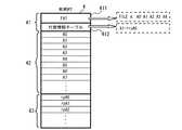
図7は、記憶領域の一部に代替ページ情報を格納したメモリを示す図である。このメモリは、ファイル管理情報領域91とデータ領域92と予備領域93を備えている。データ領域92および予備領域93は、図に示すように、ページ単位のエリアで管理されている。ファイル管理情報領域91には、FAT(File Allocation Table)が記録されている。FATは、データ領域92に格納されたファイルのチェーン情報を管理している。つまり、1つのファイルが、データ領域92の複数のページ領域に格納されており、FATには、ファイルが格納されているページのチェーン情報が記録されるのである。 FIG. 7 is a diagram showing a memory in which substitute page information is stored in a part of the storage area. This memory includes a file
たとえば、ファイルX1が、ページアドレスA0からページアドレスA5までの6つのページ領域に格納されているとする。この場合、FATには、ファイルX1の格納情報としてA0→A1→A2→A3→A4→A5というページのチェーン情報が記録されるのである。これにより、ファイルシステムは、FATを参照することで、ファイルを読み出すことが可能となる。 For example, assume that file X1 is stored in six page areas from page address A0 to page address A5. In this case, the chain information of the page A0 → A1 → A2 → A3 → A4 → A5 is recorded in the FAT as the storage information of the file X1. Thereby, the file system can read the file by referring to the FAT.
そして、データ領域92の各記憶領域には、それぞれ代替情報格納領域92aが設けられている。データ領域92の記憶領域が不良領域である場合には、その不良領域に対応する代替情報格納領域92aに予備領域93のアドレス情報が記録されるのである。これにより、データ領域92に不良領域が存在した場合にも、代替情報格納領域92aを参照することで、ファイルを読み出すことが可能となるのである。図では、たとえば、ページアドレスA1の代替情報格納領域92aに、rpA0と記録されている。したがって、ページアドレスA1が不良領域であり、ページアドレスA1に格納すべきデータが、予備領域93のページアドレスrpA0に格納されていることを示している。 In each storage area of the
一般的にこのようなメモリを使用する場合、システムは、メモリへのアクセスの際に代替ページ情報をキャッシュに確保するようにしている。そして、ファイルの読み出し時には、まず、FATを参照して、ページアドレスのチェーン情報を取得し、次に、キャッシュしている代替ページ情報を参照してページアドレスがヒットするかどうか確認するようにしている。このように、代替ページに格納されたファイルにアクセスする手段をソフトウェア実装することにより、低コストでノンパーフェクトメモリを利用できるようにしている。 In general, when such a memory is used, the system reserves alternative page information in a cache when accessing the memory. When reading a file, first, the FAT is referred to obtain the page address chain information, and then the cached alternative page information is referenced to check whether the page address hits. Yes. As described above, the non-perfect memory can be used at a low cost by installing software for accessing the file stored in the alternative page.
しかし、上述したように、代替ページ情報をキャッシュし、ソフトウェア処理により、ページがヒットするかどうかを演算する方法は、ソフトウェア処理のオーバーヘッドが発生するという問題があった。 However, as described above, the method of caching alternative page information and calculating whether a page is hit by software processing has a problem in that software processing overhead occurs.
また、不良部分に対する代替処理に伴いアドレスが不連続になった場合には、システムとして転送効率の良いDMA転送を有効に利用できないという問題があった。 Further, when the address becomes discontinuous due to the substitution process for the defective portion, there is a problem that the DMA transfer with high transfer efficiency cannot be effectively used as a system.
たとえば、図7で示したファイルX1をメモリに格納する場合を考える。まず、メモリがパーフェクトメモリ(不良領域の存在しないメモリ)である場合には、データ領域92の連続領域A0,A1,A2,A3,A4,A5にファイルX1が格納される。したがって、アドレスのインクリメントを行うことにより、1回のDMA転送により、ファイルX1を読み出すことが可能である。 For example, consider a case where the file X1 shown in FIG. 7 is stored in a memory. First, when the memory is a perfect memory (a memory having no defective area), the file X1 is stored in the continuous areas A0, A1, A2, A3, A4, and A5 of the
ところが、メモリがノンパーフェクトメモリであって、図に示したように、アドレスA1が不良領域であり、アドレスrpA0に代替されている場合、
(1)A0の読み出し、
(2)rpA0の読み出し、
(3)A2,A3,A4,A5の読み出し、
というように、ファイルX1を読み出すためには、3回のDMA転送が必要となる。つまり、連続アドレスに格納されている場合には、アドレスのインクリメントを行うことにより、DMAバースト転送が可能であるが、アドレスが不連続な場合には、一旦DMA転送を終了し、再び割り込みを発生させた後、DMA転送を行う必要があるからである。However, if the memory is a non-perfect memory and the address A1 is a defective area and is replaced with the address rpA0 as shown in the figure,
(1) Reading A0,
(2) Reading rpA0,
(3) Reading of A2, A3, A4, A5,
Thus, to read the file X1, three DMA transfers are required. In other words, DMA burst transfer is possible by incrementing the address when it is stored in continuous addresses, but if the address is discontinuous, DMA transfer is once terminated and an interrupt is generated again. This is because it is necessary to perform DMA transfer after the transfer.
また、メモリがノンパーフェクトメモリであり、アドレスA1がアドレスrpA0に代替されるだけでなく、さらに、アドレスA3がアドレスrpA1に代替されていれば、ファイルX1を読み出すために5回のDMA転送が必要となる。 If the memory is a non-perfect memory and not only the address A1 is replaced with the address rpA0 but also the address A3 is replaced with the address rpA1, five DMA transfers are required to read the file X1. It becomes.
開発効率、製造効率の面から、同じプログラムについては、同一のROMコードを用いることが好ましい。また、管理上の観点からも同一のROMコードが用いられることが好ましい。しかし、同一のROMコードを用いてプログラムをメモリに格納した場合、上記の理由から、メモリがパーフェクトメモリである場合とノンパーフェクトメモリである場合とで、パフォーマンスに差が生じるという問題があった。 From the viewpoint of development efficiency and manufacturing efficiency, it is preferable to use the same ROM code for the same program. Also, from the viewpoint of management, it is preferable that the same ROM code is used. However, when the program is stored in the memory using the same ROM code, there is a problem in that there is a difference in performance between the case where the memory is a perfect memory and the case where the memory is a non-perfect memory.
この他にノンパーフェクトメモリを使用したシステムのパフォーマンスを上げる方法として、代替ページ処理の全てをハードウェアで行う方法が考えられる。しかし、ハードウェア実装は、コストが高くなるという問題がある。 In addition, as a method of improving the performance of a system using a non-perfect memory, a method of performing all of the alternative page processing by hardware can be considered. However, the hardware implementation has a problem of high cost.
そこで、本発明は前記問題点に鑑み、不良領域の存在するメモリに格納されたファイルに効率良くアクセスするための技術を提供することを目的とする。さらには、メモリがノンパーフェクトメモリであるか否かによってパフォーマンスに差が生じないシステムを提供することを課題とする。 In view of the above problems, an object of the present invention is to provide a technique for efficiently accessing a file stored in a memory in which a defective area exists. It is another object of the present invention to provide a system in which a difference in performance does not occur depending on whether or not the memory is a non-perfect memory.
請求項1記載の発明は、ファイルが格納される記憶装置であって、ファイル管理情報を格納する第1領域と、ファイルの実体データが格納される第2領域と、を備え、前記第2領域は、ファイルの実体データが格納されるデータ領域と、前記データ領域の中に代替を必要とする領域が存在する場合に、代替的に実体データの格納領域として使用される代替領域と、を備え、前記ファイル管理情報は、前記記憶装置にアクセスするファイルシステムによって読み出される情報であり、前記ファイル管理情報には、前記代替を必要とする領域と前記代替領域との対応情報が含まれることを特徴とする。 The invention according to
請求項2記載の発明は、請求項1に記載の記憶装置において、前記ファイル管理情報には、前記代替を必要とする領域がないとした場合のファイルのチェーン情報と、前記代替を必要とする領域と前記代替領域との対応情報とが含まれることを特徴とする。 According to a second aspect of the present invention, in the storage device according to the first aspect, the file management information requires file chain information when there is no area requiring the replacement, and the replacement is required. Correspondence information between the area and the alternative area is included.
請求項3記載の発明は、請求項1に記載の記憶装置において、前記ファイル管理情報には、前記代替を必要とする領域が前記代替領域に代替された結果のファイルのチェーン情報を含むことを特徴とする。 According to a third aspect of the present invention, in the storage device according to the first aspect, the file management information includes chain information of a file obtained as a result of replacing the area requiring replacement with the replacement area. Features.
請求項4記載の発明は、請求項1ないし請求項3のいずれかに記載の記憶装置において、前記記憶装置は半導体メモリであって、ページ単位で前記代替を必要とする領域が前記代替領域に代替されることを特徴とする。 According to a fourth aspect of the present invention, in the storage device according to any one of the first to third aspects, the storage device is a semiconductor memory, and an area that requires the replacement in units of pages is the replacement area. It is characterized by being replaced.
請求項5記載の発明は、請求項1ないし請求項4のいずれかに記載の記憶装置に記憶された情報を処理する情報処理装置であって、前記記憶装置に記憶された情報を処理するホストシステムと、前記記憶装置に対するアクセスを制御するコントローラと、を備え、前記ホストシステムは、前記記憶装置に記憶された情報を管理するファイルシステム、を含み、前記コントローラは、前記ファイル管理情報から得られたファイルのページインデックスを格納するページインデックスバッファと、前記ホストシステムから前記ファイルに対する読み出しコマンドを入力した場合、前記読み出しコマンドのアドレス部を前記ページインデックスバッファに格納されているページインデックスに順次置き換えた上で、前記記憶装置に対して連続して読み出しコマンドを転送する変換手段と、を備えることを特徴とする。 A fifth aspect of the present invention is an information processing apparatus for processing information stored in the storage device according to any one of the first to fourth aspects, wherein the host processes information stored in the storage device. And a controller that controls access to the storage device, wherein the host system includes a file system that manages information stored in the storage device, and the controller is obtained from the file management information When a page index buffer for storing a page index of a file and a read command for the file are input from the host system, the address part of the read command is sequentially replaced with a page index stored in the page index buffer. Then, read continuously from the storage device. Conversion means for transferring command out, characterized in that it comprises a.
請求項6記載の発明は、請求項5に記載の情報処理装置において、前記ファイルシステムによって前記記憶装置に格納されている前記ファイルのページインデックスが読み出され、ソフトウェア処理によって読み出されたページインデックスが前記ページインデックスバッファに格納され、前記変換手段がハードウェアによって構成されていることを特徴とする。 According to a sixth aspect of the present invention, in the information processing apparatus according to the fifth aspect, a page index of the file stored in the storage device is read by the file system and is read by software processing. Is stored in the page index buffer, and the conversion means is configured by hardware.
請求項7記載の発明は、請求項5または請求項6に記載の情報処理装置において、前記ホストシステムは、DMAコントローラ、を含み、前記ホストシステムから出力される前記ファイルの読み出しコマンドは、前記DMAコントローラにより制御され、前記変換手段により順次置き換えられるページインデックスについてバースト転送が行われることを特徴とする。 According to a seventh aspect of the present invention, in the information processing apparatus according to the fifth or sixth aspect, the host system includes a DMA controller, and the read command of the file output from the host system is the DMA A burst transfer is performed for page indexes controlled by a controller and sequentially replaced by the conversion means.
請求項8記載の発明は、請求項7に記載の情報処理装置において、前記記憶装置には代替を必要とする領域が存在することにより、不連続なページアドレスに格納された不連続ファイルが記憶されており、前記ページインデックスバッファには、前記不連続ファイルの不連続なページインデックスが格納され、前記変換手段によって、読み出しコマンドのアドレス部が不連続なページインデックスに置き換えられることにより、前記DMAコントローラは、1回のバースト転送により前記不連続ファイルを読み出すことを特徴とする。 According to an eighth aspect of the present invention, in the information processing apparatus according to the seventh aspect, a discontinuous file stored at a discontinuous page address is stored because the storage device has an area that requires substitution. In the page index buffer, a discontinuous page index of the discontinuous file is stored, and an address part of a read command is replaced with a discontinuous page index by the conversion means, whereby the DMA controller Is characterized in that the discontinuous file is read out by one burst transfer.
請求項9記載の発明は、請求項1ないし請求項4のいずれかに記載の記憶装置において、前記代替を必要とする領域は、前記データ領域の中の不良領域、を含むことを特徴とする。 According to a ninth aspect of the present invention, in the storage device according to any one of the first to fourth aspects, the area requiring the replacement includes a defective area in the data area. .
請求項10記載の発明は、請求項1ないし請求項4のいずれかに記載の記憶装置において、前記代替を必要とする領域は、更新が必要とされるデータが記録されている領域、を含み、前記代替領域に更新後のデータが記録されることによって、データ更新が行われることを特徴とする。 According to a tenth aspect of the present invention, in the storage device according to any one of the first to fourth aspects, the area requiring replacement includes an area in which data that needs to be updated is recorded. The data update is performed by recording the updated data in the alternative area.
本発明の記憶装置は、ファイル管理情報に、代替を必要とする領域と代替領域との対応情報が含まれるので、ファイルシステムが代替情報を取得することが可能である。これにより、ファイルアクセス処理の上位の工程において、代替情報が処理され、効率のよいファイルアクセスが行われる。 In the storage device of the present invention, the file management information includes correspondence information between the area requiring replacement and the replacement area, so that the file system can acquire the replacement information. As a result, the substitute information is processed in an upper process of the file access process, and efficient file access is performed.
また、本発明の情報処理装置は、読み出しコマンドのアドレス部をページインデックスバッファに格納されているページインデックスに順次置き換えた上で、記憶装置に対して連続して読み出しコマンドを転送するので、不良領域の存在により、不連続なエリアに格納されているファイルに対しても効率良くアクセスすることが可能である。 Further, the information processing apparatus according to the present invention sequentially replaces the address portion of the read command with the page index stored in the page index buffer, and continuously transfers the read command to the storage device. Therefore, it is possible to efficiently access a file stored in a discontinuous area.
以下、図面を参照しつつ本発明の実施の形態について説明する。図1は、本発明の実施の形態に係る情報処理装置1の機能ブロック図である。情報処理装置1は、メモリ4に格納されているファイルを読み込んで様々な情報処理を行う装置である。本実施の形態において、メモリ4は、フラッシュメモリ等の半導体メモリである。 Hereinafter, embodiments of the present invention will be described with reference to the drawings. FIG. 1 is a functional block diagram of an
また、本実施の形態において、情報処理装置1は、メモリ4をFATファイルシステムによって管理している。メモリ4は、図に示すように、ファイル管理情報領域41とデータ領域42と予備領域43を備えている。 In the present embodiment, the
データ領域42は、複数のページ領域421に区画されており、プログラムファイルやデータファイルの実体が格納される。そして、このメモリ4には、ページ単位でデータのアクセスが行われる。また、予備領域43は、複数のページ領域431に区画されて管理されている。本実施の形態において、メモリ4は、その一部の格納領域に不良領域が存在する可能性のあるメモリを対象としている。つまり、データ領域42に含まれるページ領域の中に不良領域が存在する可能性がある。そして、データ領域42に不良領域が存在した場合に、その代替領域として利用されるのが予備領域43である。 The
ファイル管理情報領域41には、FAT(File Allocation Table)411と代替情報テーブル412が格納されている。FAT411は、ファイルの格納情報が記録されている。具体的には、ファイルが格納されているページのチェーン情報が記録されている。代替情報テーブル412については、後で詳しく説明する。 The file
情報処理装置1は、たとえば、ゲーム装置である。この場合、メモリ4はゲームカートリッジであり、ゲーム装置である情報処理装置1は、メモリ4に格納されたゲームプログラムを実行する。 The
情報処理装置1は、ホストシステム2とメモリコントローラ3とを備えている。ホストシステム2は、情報処理装置1の全体制御を行う中枢処理部であり、CPU21、DMAC(Direct Memory Access Controller)22、ROM23を備えている。ROM23には、後述する各種のソフトウェアが格納されている。また、情報処理装置1は、この他に、各種の入力装置や出力装置などを備えている。情報処理装置1が、ゲーム装置である場合には、出力装置として液晶表示装置やスピーカなどを備える。また、入力装置としては、各種の操作ボタンを備える。 The
メモリコントローラ3は、ホストインタフェース31と、ページインデックスバッファ32と、コマンドテンプレート生成部33と、ページインデックス転送シーケンサ34とを備えている。 The
ホストインタフェース31は、ホストシステム2との間でコマンドやデータの入出力を行うインタフェースである。つまり、ホストインタフェース31は、ホストシステム2からアドレス部を指定した読み出しコマンドや書き込みコマンドを入力するインタフェースであり、また、メモリ4から読み出されたデータをホストシステム2に出力するインタフェースである。 The
ページインデックスバッファ32は、読み出し対象であるファイルのページインデックスを格納するバッファである。つまり、読み出し対象であるファイルが格納されている全ページの情報が記録されるバッファである。上述したように、ファイルは、メモリ4の複数のページ領域に格納されることになるが、ページインデックスとは、ファイルが格納されているページ領域を指定した情報である。より具体的には、ページインデックスとは、ファイルが格納されているページ領域のアドレスを指定した情報である。なお、後述するように、ページインデックスバッファ32に格納されるアドレスは、メモリ4の物理アドレスである。このページインデックスバッファ32には、不連続なページに格納されたファイルについては、不連続な物理アドレスがそのまま記録される。 The
コマンドテンプレート生成部33は、ページインデックス転送シーケンサ34において生成する読み出しコマンドのテンプレートを作成する。そして、ページインデックス転送シーケンサ34は、コマンドテンプレート生成部33によって生成されたコマンドのアドレス部を、ページインデックスバッファ32に格納されているページインデックスに置き換えた上で、メモリ4に読み出しコマンドを出力する。コマンドテンプレート生成部33およびページインデックス転送シーケンサ34は、ハードウェアで構成されている。 The command
図2は、情報処理装置1の構成をソフトウェア層とハードウェア層に分類して示した図である。ソフトウェア層は、図に示すように、上位のアプリケーション層、アプリケーションの下位に位置するAPI(Application Program Interface)層、ドライバ層から構成され、ドライバ層の下位にハードウェア層が位置している。本実施の形態においては、アプリケーション層は、たとえば、ゲームプログラムなどのアプリケーションプログラムであり、API層は、FATシステムであり、ドライバ層は、メモリコントローラ3を制御するドライバ(デバイスドライバ)である。 FIG. 2 is a diagram showing the configuration of the
なお、アプリケーションプログラムは、メモリ4に格納されている。また、FATシステムは、プログラムとメモリ4に記録されているテーブルなどの情報(ファイル管理情報領域41に格納されている情報)から構成されるが、そのプログラム部分は、ROM23に格納されている。また、ドライバもROM23に格納されている。 The application program is stored in the
次に、代替情報テーブル412について説明する。上述したように、メモリ4のデータ領域42は、複数のページ領域421に区画されており、メモリ4は、ページ単位でアクセス制御される。つまり、ページ単位で、データの読み出し処理や書き込み処理が実行される。したがって、1つのファイルが複数のページ領域421に分割して格納される場合には、FAT411には、各ファイルのページチェーン情報が記録される。 Next, the alternative information table 412 will be described. As described above, the
図3は、メモリ4にファイルAが格納されている状態を示す図である。ファイルAは、データ領域42の5つのページアドレスA0,A1,A2,A3,A4に格納されている。したがって、FAT411には、ファイルAの格納情報として、A0→A1→A2→A3→A4というページのチェーン情報が記録されている。 FIG. 3 is a diagram illustrating a state in which the file A is stored in the
そして、この図で示した例では、ページアドレスA1の記憶領域が不良領域であるものとする。そこで、代替情報テーブル412には、ページアドレスA1が不良領域であり、その代替領域のアドレスはrpA0であることを示す情報が記録されている。 In the example shown in this figure, it is assumed that the storage area of the page address A1 is a defective area. Therefore, the substitution information table 412 records information indicating that the page address A1 is a defective area and the address of the substitution area is rpA0.
この代替情報テーブル412は、ファイルシステムによってアクセスされる領域である。本実施の形態であれば、FATファイルシステムによってアクセスされる領域である。つまり、ホストシステムがメモリ4にアクセスする際に、まず、FATファイルシステムによって、ファイル管理情報領域41が読み出されるが、その際、FAT411とともに読み出される領域である。 This alternative information table 412 is an area accessed by the file system. In the present embodiment, the area is accessed by the FAT file system. In other words, when the host system accesses the
つまり、本実施の形態におけるメモリ4は、不良領域が存在した場合、ファイルの格納時に、ファイルシステムによって管理される代替情報テーブル412に代替情報が記録されるのである。このため、ファイルの読み出し処理の上位の工程であるファイルシステムによるFAT411の参照時に、あわせて代替情報を取得することができ、処理の効率化が図られるのである。 That is, in the
なお、この実施の形態においては、FAT411に、ファイルの予定されていた格納アドレス情報を記録し、このFAT411とは別に、代替情報テーブル412に代替情報を格納するようにした。言い換えると、ファイル管理情報領域41には、不良領域がないとした場合のファイルのチェーン情報がFAT411に記録され、それとは別に不良領域と代替領域の対応情報が代替情報テーブル412に記録されている。別の実施例として、これらの情報を1つの情報に統合して記録するようにしてもよい。つまり、不良領域を代替領域に代替した結果のファイルチェーン情報をファイル管理情報領域41に記録するようにしてもよい。図3の例であれば、ファイル管理情報領域41に、ファイルAのチェーン情報として、アドレスA0→rpA0→A2→A3→A4を記録するようにしてもよい。 In this embodiment, the storage address information on which the file is scheduled is recorded in the
以上の構成のもと、本実施の形態の情報処理装置1によるメモリアクセス処理の流れを図4のフローチャートを参照しながら説明する。ここでは、メモリ4には、図3で説明したような状態でファイルAが記録されているものとする。つまり、ファイルAは、ページアドレスA0,rpA0,A2,A3,A4に格納されている。 With the above configuration, the flow of memory access processing by the
なお、ページアドレスA0〜A7は、メモリ4のFAT411に記録された論理アドレスである。ただし、本実施の形態においては、メモリ4のFAT411に記録された論理アドレスは、メモリ4の物理アドレスと1対1に対応している。したがって、本実施の形態においては、ファイルAは、論理アドレスとしても、また、物理アドレスとしても、不連続なページに格納されている。 The page addresses A0 to A7 are logical addresses recorded in the
アプリケーションプログラムが、ファイルAを読み出す処理について説明する。まず、アプリケーションプログラムが、ファイルAを読み出す命令を実行する(ステップS1)。実質的には、この命令はCPU21によって実行される。 A process in which the application program reads file A will be described. First, the application program executes a command for reading the file A (step S1). In effect, this instruction is executed by the
次に、FATシステムが、メモリ4にアクセスし、メモリ4に記録されているFAT411および代替情報テーブル412を参照する。そして、ファイルAが格納されている論理アドレスのチェーン情報(ページアドレスのチェーン情報)および不良領域の代替情報を取得する(ステップS2)。つまり、ファイルAが、論理アドレスA0,A1,A2,A3,A4に格納されているというチェーン情報をFAT411から取得するとともに、ページアドレスA1の記憶領域がページアドレスrpA0に代替されているという情報を代替情報テーブル412から得る。 Next, the FAT system accesses the
FATシステムが取得したファイルAの格納アドレス情報は、ドライバに渡される。つまり、ファイルAが、アドレスA0,rpA0,A2,A3,A4に格納されているという情報がドライバに渡される。そして、ドライバは、ファイルAの格納論理アドレスを物理アドレスに変換する(ステップS3)。この論理―物理変換を行うために、ホストシステム2は、ページアドレスの対応テーブルを保持している。 The storage address information of the file A acquired by the FAT system is passed to the driver. That is, information that the file A is stored at addresses A0, rpA0, A2, A3, and A4 is passed to the driver. Then, the driver converts the storage logical address of file A into a physical address (step S3). In order to perform this logical-physical conversion, the
ドライバは、ファイルAの格納物理アドレスを得ると、この物理アドレスを、ページインデックスバッファ32に格納する(ステップS4)。図5は、ページインデックスバッファ32に格納されたファイルAのインデックスを示している。図に示すように、インデックス0〜インデックス4に対応した記憶領域に、物理アドレスA0,rpA0,A2,A3,A4が格納されている。なお、上述したように、この実施の形態においては、論理アドレスと物理アドレスとは1対1に対応しているので、ページインデックスバッファ32に格納されるアドレスの符号についても、説明を簡単にするために、同じアドレスの符号A0,rpA0,A2,A3,A4を用いている。 When the driver obtains the storage physical address of file A, it stores this physical address in the page index buffer 32 (step S4). FIG. 5 shows the index of the file A stored in the
また、ドライバは、ファイルAのページ数情報をページインデックス転送シーケンサ34に与える(ステップS5)。この場合であれば、ファイルAは、メモリ4の5つのページ領域に格納されているので、ページ数情報「5」をページインデックス転送シーケンサ34に与える。ページインデッックス転送シーケンサ34は、バッファを持っており、ドライバから受け取ったファイルのページ数情報を格納する。 Further, the driver gives page number information of the file A to the page index transfer sequencer 34 (step S5). In this case, since the file A is stored in the five page areas of the
さらに、ドライバは、コマンドテンプレート生成部33に対して、コマンドのテンプレートを設定する(ステップS6)。つまり、メモリ4に対する読み出しコマンドのフォーマットを指定する。具体的には、命令部の開始ビット位置、ビット数、アドレス部の開始ビット位置、ビット数などを設定する。 Further, the driver sets a command template to the command template generation unit 33 (step S6). That is, the format of the read command for the
以上で、読み出しコマンドの出力の準備が終わり、次に、DMAC22によりDMA転送コマンドが出力される(ステップS7)。このコマンドは、ファイルAを読み出すコマンドであるが、コマンドには、読み出しコマンドを示す命令語を指定するだけでよい。読み出しアドレスは指定する必要はない。 Thus, the preparation for outputting the read command is completed, and then the
DAMC22により出力された読み出しコマンドは、ホストインタフェース31を介して、コマンドテンプレート生成部33に渡される。ここで、読み出しコマンドは、コマンドテンプレートによりマスクされて、アドレス部がクリアされる(ステップS8)。 The read command output by the
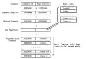
図6は、読み出しコマンドの変換内容を示す図である。図中、「Command」は、DMAC22より出力された読み出しコマンドを示している。このコマンドには、“Command ID”として、読み出し命令(Read)を示すコード(“01234567”(16進数))が指定されている。また、アドレス部は、特に指定する必要がないため、意味のないコード(“11223344”(16進数))が含まれている。 FIG. 6 is a diagram showing the conversion contents of the read command. In the drawing, “Command” indicates a read command output from the
図中、「Command Template」は、コマンドテンプレート生成部33において生成されたコマンドテンプレートである。このコマンドテンプレートは、コマンド中の命令部に全てF(16進数)が指定され、アドレス部には、全て0(16進数)が指定されている。 In the figure, “Command Template” is a command template generated by the command
そして、DMAC22から出力された「Command」が、「Command Template」でマスクされることによって、得られるのが、「Masked Command」である。つまり、「Command」と「Command Template」で論理積をとることによって、得られるのが「Masked Command」であり、アドレス部が0にクリアされている。 Then, “Masked Command” is obtained by masking the “Command” output from the
次に、マスクされた読み出しコマンドがページインデックス転送シーケンサ34に出力される。ページインデックス転送シーケンサ34は、ドライバから取得したページ数情報に基づいてページインデックスバッファ32から、ファイルAのページインデックスを取得する(ステップS9)。ここでは、ドライバからページ数情報「5」を得ているので、ページインデックスバッファ32に格納されている5つの領域のインデックスを取得する。つまり、物理アドレスA0,rpA0,A2,A3,A4を取得する。 Next, the masked read command is output to the page
そして、ページインデックス転送シーケンサ34は、ページインデックスバッファ32から取得したインデックスを、1アドレスずつ、マスクされた読み出しコマンドのアドレス部にセットし、メモリ4に対して出力するのである(ステップS10)。この例であれば、まず、物理アドレスA0をアドレス部にセットした読み出しコマンドをメモリ4に出力し、続いて、物理アドレスrpA0をアドレス部にセットした読み出しコマンドをメモリ4に出力し、順に、物理アドレスA2,A3,A4をセットした読み出しコマンドをメモリ4に出力するのである。つまり、ページインデックス転送シーケンサ34は、DMAC22から1つのファイル読み出しコマンドを受け取ると、ページインデックスバッファ32から受け取った全てのページインデックスについて連続的に、読み出しコマンドを出力するのである。 Then, the page
これにより、メモリ4からは、順次、物理アドレスA0,rpA0,A2,A3,A4に格納されていたデータが出力される。このデータは、ホストインタフェース31を介してホストシステム2に渡されるのである。このようにして、ファイルAの読み出し処理が終了する。 Thereby, the data stored in the physical addresses A0, rpA0, A2, A3, and A4 are sequentially output from the
このように、本実施の形態によれば、ファイルが不連続な論理アドレスに格納されている場合にも、DMAバースト転送が可能であり、ファイルの読み出し速度を向上させることが可能である。 Thus, according to the present embodiment, DMA burst transfer is possible even when a file is stored at discontinuous logical addresses, and the file reading speed can be improved.
また、本実施の形態のメモリ4および情報処理装置1を利用することにより、パーフェクトメモリとノンパーフェクトメモリとで同一のROMコードを利用可能である。つまり、図3で示したFAT411に記録されるデータとデータ領域42に格納されるデータとを共通のROMコードとして製作するのである。そして、パーフェクトメモリに格納される場合には、このROMコードが記録されたメモリが、そのままプログラムメモリとなる。一方、ノンパーフェクトメモリに格納される場合には、この共通のROMコード部分に、代替情報テーブル412と予備領域43に記録される情報が付加されればよいのである。これにより、たとえばゲームプログラムを格納したメモリの製造工程において、生産性の向上、コストの削減などを図ることが可能である。 Further, by using the
なお、上記の実施の形態においては、メモリ4がノンパーフェクトメモリであり、代替情報テーブル412には、不良領域に対する代替情報が書き込まれることを説明した。たとえば、情報処理装置1がゲーム機であり、メモリ4が、1回のみデータ書き込み可能なOTP(One Time Programmable)メモリである場合などが考えられる。つまり、OTPメモリにゲームプログラムを格納してユーザに供給するという形態である。大容量化の進むOTPメモリには、不良領域が含まれている場合があるが、ゲームプログラムは、共通のROMコードを製作するだけでよい。この共通のROMコードを用いて、ノンパーフェクトメモリであるOTPメモリにゲームプログラムを格納してもよいし、他のパーフェクトメモリにゲームプログラムを格納してもよい。 In the above embodiment, it has been described that the
また、この発明の応用例として、代替情報テーブル412を利用して、ファイルの更新処理を行うことが可能である。OTPメモリを利用してプログラムメモリを供給することを説明したが、OTPメモリには、追記が可能なものがある。この場合、FATの情報を修正することはできないため、ファイルの追加は不可能であるが、最初にFATに記録されたファイルについては、代替情報テーブル412および予備領域43に情報を追記することで、ファイルの内容を実質的に更新することが可能である。 Further, as an application example of the present invention, it is possible to perform a file update process using the alternative information table 412. Although it has been described that the program memory is supplied using the OTP memory, some OTP memories can be additionally written. In this case, since the FAT information cannot be corrected, it is impossible to add a file. However, by adding information to the alternative information table 412 and the
言い換えると、本発明は、メモリに不良領域が存在する場合のみならず、広い意味で代替が必要な領域が存在する場合に、有効な発明である。代替を必要とする領域が、不良領域である場合には、上述したように、ROMコードの作成時に生産性が向上するなど、メーカー側にとって多くのメリットが存在する。これに対して、代替を必要とする領域が、更新が必要なデータが格納されている領域である場合には、追記可能なOTPメモリにおいて、ファイルの更新が可能となり、ユーザにとって多くのメリットがある。 In other words, the present invention is effective not only when there is a defective area in the memory but also when there is an area that needs to be replaced in a broad sense. When the area that needs to be replaced is a defective area, as described above, there are many merits for the manufacturer, such as an improvement in productivity when creating a ROM code. On the other hand, if the area that needs to be replaced is an area that stores data that needs to be updated, the file can be updated in the additionally recordable OTP memory, which has many advantages for the user. is there.
また、上記の実施の形態において、ページインデックスの取得と、バッファへの格納は、ファイルシステムやドライバなどのソフトウェアによって処理し、コマンドのアドレス部の置き換えは、ハードウェアであるページインデックス転送シーケンサ34によって処理するようにした。つまり、ハードウェアかに不向きな高位の機能はファイルシステムの一部として実装し、ハードウェアに適した低位な機能である連続ページ読み出し処理は、シーケンサおよびバッファ(レジスタ)として実装することによって、ソフトウェアとハードウェアがそれぞれ得意とする処理がバランスよく負荷分散し、高機能かつ効率のよいシステムが構築される。 In the above embodiment, acquisition of the page index and storage in the buffer are processed by software such as a file system and a driver, and replacement of the address part of the command is performed by the page
なお、上記の実施の形態においては、ページインデックスを置き換えることにより、DMAバースト転送を行う場合を例に説明したが、本発明は、DMA転送のみならず、CPUによる転送にも適用可能である。つまり、上記の実施の形態において、DMAC22を用いることなく、CPU21より読み出しコマンドを発生させ、CPU21より発生した読み出しコマンドのアドレス部を、図6等で示したように、ページインデックスで置き換えるようにしてもよい。 In the above embodiment, the case where DMA burst transfer is performed by replacing the page index has been described as an example. However, the present invention can be applied not only to DMA transfer but also to transfer by a CPU. That is, in the above embodiment, a read command is generated from the
また、本発明は、ファイルが格納されているページの論理アドレスが不連続の場合に、効果を奏するものであるが、上記の実施の形態で示したように、論理アドレスと物理アドレスが1対1に対応している場合には、ファイルは、物理アドレスについても不連続なページに格納されている。したがって、論理、物理いずれのアドレスについても不連続な場合にも適用可能である。 In addition, the present invention is effective when the logical address of the page in which the file is stored is discontinuous. As shown in the above embodiment, the logical address and the physical address are paired. In the case of corresponding to 1, the file is stored in discontinuous pages with respect to physical addresses. Therefore, the present invention can be applied to a case where both logical and physical addresses are discontinuous.
1 情報処理装置
2 ホストシステム
3 メモリコントローラ
4 メモリ
41 ファイル管理情報領域
42 データ領域
43 予備領域
411 FAT
412 代替情報テーブルDESCRIPTION OF
412 Alternative information table
Claims (10)
Translated fromJapaneseファイル管理情報を格納する第1領域と、
ファイルの実体データが格納される第2領域と、
を備え、
前記第2領域は、
ファイルの実体データが格納されるデータ領域と、
前記データ領域の中に代替を必要とする領域が存在する場合に、代替的に実体データの格納領域として使用される代替領域と、
を備え、
前記ファイル管理情報は、前記記憶装置にアクセスするファイルシステムによって読み出される情報であり、前記ファイル管理情報には、前記代替を必要とする領域と前記代替領域との対応情報が含まれることを特徴とする記憶装置。A storage device for storing files,
A first area for storing file management information;
A second area for storing file entity data;
With
The second region is
A data area for storing the actual data of the file;
When there is an area that needs to be replaced in the data area, an alternative area that is alternatively used as a storage area for entity data;
With
The file management information is information read by a file system that accesses the storage device, and the file management information includes correspondence information between the area requiring replacement and the replacement area. Storage device.
前記ファイル管理情報には、前記代替を必要とする領域がないとした場合のファイルのチェーン情報と、前記代替を必要とする領域と前記代替領域との対応情報とが含まれることを特徴とする記憶装置。The storage device according to claim 1,
The file management information includes file chain information in a case where there is no area that requires substitution, and correspondence information between the area that requires substitution and the substitution area. Storage device.
前記ファイル管理情報には、前記代替を必要とする領域が前記代替領域に代替された結果のファイルのチェーン情報を含むことを特徴とする記憶装置。The storage device according to claim 1,
The storage device characterized in that the file management information includes chain information of a file as a result of replacing the area requiring replacement with the replacement area.
前記記憶装置は半導体メモリであって、ページ単位で前記代替を必要とする領域が前記代替領域に代替されることを特徴とする記憶装置。The storage device according to any one of claims 1 to 3,
The storage device is a semiconductor memory, and an area that requires the replacement in units of pages is replaced with the replacement area.
前記記憶装置に記憶された情報を処理するホストシステムと、
前記記憶装置に対するアクセスを制御するコントローラと、
を備え、
前記ホストシステムは、
前記記憶装置に記憶された情報を管理するファイルシステム、
を含み、
前記コントローラは、
前記ファイル管理情報から得られたファイルのページインデックスを格納するページインデックスバッファと、
前記ホストシステムから前記ファイルに対する読み出しコマンドを入力した場合、前記読み出しコマンドのアドレス部を前記ページインデックスバッファに格納されているページインデックスに順次置き換えた上で、前記記憶装置に対して連続して読み出しコマンドを転送する変換手段と、
を備えることを特徴とする情報処理装置。An information processing apparatus for processing information stored in a storage device according to any one of claims 1 to 4,
A host system for processing information stored in the storage device;
A controller for controlling access to the storage device;
With
The host system is
A file system for managing information stored in the storage device;
Including
The controller is
A page index buffer for storing a page index of a file obtained from the file management information;
When a read command for the file is input from the host system, the address part of the read command is sequentially replaced with a page index stored in the page index buffer, and then the read command is continuously sent to the storage device. Conversion means for transferring
An information processing apparatus comprising:
前記ファイルシステムによって前記記憶装置に格納されている前記ファイルのページインデックスが読み出され、ソフトウェア処理によって読み出されたページインデックスが前記ページインデックスバッファに格納され、前記変換手段がハードウェアによって構成されていることを特徴とする情報処理装置。The information processing apparatus according to claim 5,
A page index of the file stored in the storage device is read by the file system, a page index read by software processing is stored in the page index buffer, and the conversion unit is configured by hardware. An information processing apparatus characterized by comprising:
前記ホストシステムは、
DMAコントローラ、
を含み、
前記ホストシステムから出力される前記ファイルの読み出しコマンドは、前記DMAコントローラにより制御され、前記変換手段により順次置き換えられるページインデックスについてバースト転送が行われることを特徴とする情報処理装置。The information processing apparatus according to claim 5 or 6,
The host system is
DMA controller,
Including
The file read command output from the host system is controlled by the DMA controller, and burst transfer is performed for page indexes that are sequentially replaced by the conversion means.
前記記憶装置には代替を必要とする領域が存在することにより、不連続なページアドレスに格納された不連続ファイルが記憶されており、前記ページインデックスバッファには、前記不連続ファイルの不連続なページインデックスが格納され、前記変換手段によって、読み出しコマンドのアドレス部が不連続なページインデックスに置き換えられることにより、前記DMAコントローラは、1回のバースト転送により前記不連続ファイルを読み出すことを特徴とする情報処理装置。The information processing apparatus according to claim 7,
Since the storage device has an area that requires replacement, a discontinuous file stored at a discontinuous page address is stored, and the discontinuous file of the discontinuous file is stored in the page index buffer. A page index is stored, and the conversion unit replaces the address part of the read command with a discontinuous page index, whereby the DMA controller reads the discontinuous file by one burst transfer. Information processing device.
前記代替を必要とする領域は、
前記データ領域の中の不良領域、
を含むことを特徴とする記憶装置。The storage device according to any one of claims 1 to 4,
The area requiring the replacement is
A defective area in the data area;
A storage device comprising:
前記代替を必要とする領域は、
更新が必要とされるデータが記録されている領域、
を含み、
前記代替領域に更新後のデータが記録されることによって、データ更新が行われることを特徴とする記憶装置。
The storage device according to any one of claims 1 to 4,
The area requiring the replacement is
Area where data that needs to be updated is recorded,
Including
The storage device, wherein the updated data is recorded by recording the updated data in the alternative area.
Priority Applications (4)
| Application Number | Priority Date | Filing Date | Title |
|---|---|---|---|
| JP2005376686AJP4895264B2 (en) | 2005-12-27 | 2005-12-27 | Storage device and information processing device |
| US11/566,953US20070150528A1 (en) | 2005-12-27 | 2006-12-05 | Memory device and information processing apparatus |
| DE602006001929TDE602006001929D1 (en) | 2005-12-27 | 2006-12-06 | Storage device and information processing device |
| EP06025260AEP1804166B1 (en) | 2005-12-27 | 2006-12-06 | Memory device and information processing apparatus |
Applications Claiming Priority (1)
| Application Number | Priority Date | Filing Date | Title |
|---|---|---|---|
| JP2005376686AJP4895264B2 (en) | 2005-12-27 | 2005-12-27 | Storage device and information processing device |
Publications (2)
| Publication Number | Publication Date |
|---|---|
| JP2007179286Atrue JP2007179286A (en) | 2007-07-12 |
| JP4895264B2 JP4895264B2 (en) | 2012-03-14 |
Family
ID=37934378
Family Applications (1)
| Application Number | Title | Priority Date | Filing Date |
|---|---|---|---|
| JP2005376686AExpired - Fee RelatedJP4895264B2 (en) | 2005-12-27 | 2005-12-27 | Storage device and information processing device |
Country Status (4)
| Country | Link |
|---|---|
| US (1) | US20070150528A1 (en) |
| EP (1) | EP1804166B1 (en) |
| JP (1) | JP4895264B2 (en) |
| DE (1) | DE602006001929D1 (en) |
Cited By (1)
| Publication number | Priority date | Publication date | Assignee | Title |
|---|---|---|---|---|
| US8176103B2 (en) | 2008-03-12 | 2012-05-08 | Samsung Electronics Co., Ltd. | File access method and system |
Families Citing this family (1)
| Publication number | Priority date | Publication date | Assignee | Title |
|---|---|---|---|---|
| US9147470B1 (en)* | 2011-11-11 | 2015-09-29 | Marvell International Ltd. | NAND flash controller with programmable command templates |
Citations (23)
| Publication number | Priority date | Publication date | Assignee | Title |
|---|---|---|---|---|
| JPS63142416A (en)* | 1986-12-04 | 1988-06-14 | Fujitsu Ltd | Input/output control system |
| JPH01267750A (en)* | 1988-04-19 | 1989-10-25 | Nec Corp | System for managing storage area |
| JPH02118739A (en)* | 1988-10-28 | 1990-05-07 | Hitachi Ltd | data processing equipment |
| JPH04128947A (en)* | 1990-09-19 | 1992-04-30 | Pfu Ltd | address translation buffer device |
| JPH04259046A (en)* | 1991-02-13 | 1992-09-14 | Nec Software Ltd | Rom patch system |
| JPH08297605A (en)* | 1995-04-26 | 1996-11-12 | Hitachi Ltd | Data processing device and system using the same |
| JPH1031611A (en)* | 1996-07-15 | 1998-02-03 | Advantest Corp | File system for nonvolatile memory storage medium |
| JPH1063432A (en)* | 1996-08-22 | 1998-03-06 | Ricoh Co Ltd | File control unit |
| JPH10269141A (en)* | 1997-03-28 | 1998-10-09 | Fujitsu Ltd | Processor board circuit |
| JPH11224266A (en)* | 1997-11-10 | 1999-08-17 | Nippon Telegr & Teleph Corp <Ntt> | Electronic video document creation and utilization method and program storage medium |
| JP2000099451A (en)* | 1998-09-24 | 2000-04-07 | Fuji Xerox Co Ltd | Interface controller |
| JP2001005838A (en)* | 1997-11-10 | 2001-01-12 | Nippon Telegr & Teleph Corp <Ntt> | Electronic image document creation method and recording medium storing electronic image document creation program |
| JP2001256104A (en)* | 2000-03-14 | 2001-09-21 | Fuji Xerox Co Ltd | Information processor |
| JP2001357637A (en)* | 2000-06-14 | 2001-12-26 | Sony Corp | Information reproducing device, information processing method and information recording medium |
| JP2003077223A (en)* | 2001-09-04 | 2003-03-14 | Ricoh Co Ltd | Information recording / reproducing device |
| JP2004102981A (en)* | 2002-09-12 | 2004-04-02 | Samsung Electro Mech Co Ltd | Memory defect treatment device and its method |
| JP2004118407A (en)* | 2002-09-25 | 2004-04-15 | Renesas Technology Corp | Nonvolatile semiconductor storage device |
| JP2004246787A (en)* | 2003-02-17 | 2004-09-02 | Seiko Epson Corp | Information processing apparatus and program control method |
| JP2004265162A (en)* | 2003-03-03 | 2004-09-24 | Renesas Technology Corp | Storage device and address management method |
| JP2004280752A (en)* | 2003-03-19 | 2004-10-07 | Sony Corp | Date storage device, management information updating method for data storage device, and computer program |
| JP2005100418A (en)* | 2004-09-27 | 2005-04-14 | Renesas Technology Corp | Data processor and system using it |
| JP2005185691A (en)* | 2003-12-26 | 2005-07-14 | Fujinon Corp | Electronic endoscopic apparatus and method of forwarding program |
| JP2005196658A (en)* | 2004-01-09 | 2005-07-21 | Buffalo Inc | External storage device |
Family Cites Families (2)
| Publication number | Priority date | Publication date | Assignee | Title |
|---|---|---|---|---|
| EP0992916A1 (en)* | 1998-10-06 | 2000-04-12 | Texas Instruments Inc. | Digital signal processor |
| US6742078B1 (en)* | 1999-10-05 | 2004-05-25 | Feiya Technology Corp. | Management, data link structure and calculating method for flash memory |
- 2005
- 2005-12-27JPJP2005376686Apatent/JP4895264B2/ennot_activeExpired - Fee Related
- 2006
- 2006-12-05USUS11/566,953patent/US20070150528A1/ennot_activeAbandoned
- 2006-12-06EPEP06025260Apatent/EP1804166B1/ennot_activeNot-in-force
- 2006-12-06DEDE602006001929Tpatent/DE602006001929D1/ennot_activeExpired - Fee Related
Patent Citations (26)
| Publication number | Priority date | Publication date | Assignee | Title |
|---|---|---|---|---|
| JPS63142416A (en)* | 1986-12-04 | 1988-06-14 | Fujitsu Ltd | Input/output control system |
| JPH01267750A (en)* | 1988-04-19 | 1989-10-25 | Nec Corp | System for managing storage area |
| JPH02118739A (en)* | 1988-10-28 | 1990-05-07 | Hitachi Ltd | data processing equipment |
| JPH04128947A (en)* | 1990-09-19 | 1992-04-30 | Pfu Ltd | address translation buffer device |
| JPH04259046A (en)* | 1991-02-13 | 1992-09-14 | Nec Software Ltd | Rom patch system |
| JPH08297605A (en)* | 1995-04-26 | 1996-11-12 | Hitachi Ltd | Data processing device and system using the same |
| JPH1031611A (en)* | 1996-07-15 | 1998-02-03 | Advantest Corp | File system for nonvolatile memory storage medium |
| JPH1063432A (en)* | 1996-08-22 | 1998-03-06 | Ricoh Co Ltd | File control unit |
| JPH10269141A (en)* | 1997-03-28 | 1998-10-09 | Fujitsu Ltd | Processor board circuit |
| JPH11224266A (en)* | 1997-11-10 | 1999-08-17 | Nippon Telegr & Teleph Corp <Ntt> | Electronic video document creation and utilization method and program storage medium |
| JP2001005838A (en)* | 1997-11-10 | 2001-01-12 | Nippon Telegr & Teleph Corp <Ntt> | Electronic image document creation method and recording medium storing electronic image document creation program |
| JP2000099451A (en)* | 1998-09-24 | 2000-04-07 | Fuji Xerox Co Ltd | Interface controller |
| JP2001256104A (en)* | 2000-03-14 | 2001-09-21 | Fuji Xerox Co Ltd | Information processor |
| JP2001357637A (en)* | 2000-06-14 | 2001-12-26 | Sony Corp | Information reproducing device, information processing method and information recording medium |
| JP2003077223A (en)* | 2001-09-04 | 2003-03-14 | Ricoh Co Ltd | Information recording / reproducing device |
| US20040078700A1 (en)* | 2002-09-12 | 2004-04-22 | Samsung Electro-Mechanics Co., Ltd. | Apparatus and method for processing defects in memories |
| JP2004102981A (en)* | 2002-09-12 | 2004-04-02 | Samsung Electro Mech Co Ltd | Memory defect treatment device and its method |
| US20050141300A1 (en)* | 2002-09-25 | 2005-06-30 | Renesas Technology Corp. | Nonvolatile memory |
| JP2004118407A (en)* | 2002-09-25 | 2004-04-15 | Renesas Technology Corp | Nonvolatile semiconductor storage device |
| JP2004246787A (en)* | 2003-02-17 | 2004-09-02 | Seiko Epson Corp | Information processing apparatus and program control method |
| JP2004265162A (en)* | 2003-03-03 | 2004-09-24 | Renesas Technology Corp | Storage device and address management method |
| JP2004280752A (en)* | 2003-03-19 | 2004-10-07 | Sony Corp | Date storage device, management information updating method for data storage device, and computer program |
| US20050182892A1 (en)* | 2003-03-19 | 2005-08-18 | Kenichi Nakanishi | Data storage device, method for updating management information in data storage device, and computer program |
| JP2005185691A (en)* | 2003-12-26 | 2005-07-14 | Fujinon Corp | Electronic endoscopic apparatus and method of forwarding program |
| JP2005196658A (en)* | 2004-01-09 | 2005-07-21 | Buffalo Inc | External storage device |
| JP2005100418A (en)* | 2004-09-27 | 2005-04-14 | Renesas Technology Corp | Data processor and system using it |
Cited By (1)
| Publication number | Priority date | Publication date | Assignee | Title |
|---|---|---|---|---|
| US8176103B2 (en) | 2008-03-12 | 2012-05-08 | Samsung Electronics Co., Ltd. | File access method and system |
Also Published As
| Publication number | Publication date |
|---|---|
| EP1804166B1 (en) | 2008-07-23 |
| EP1804166A3 (en) | 2007-07-18 |
| JP4895264B2 (en) | 2012-03-14 |
| EP1804166A2 (en) | 2007-07-04 |
| DE602006001929D1 (en) | 2008-09-04 |
| US20070150528A1 (en) | 2007-06-28 |
Similar Documents
| Publication | Publication Date | Title |
|---|---|---|
| JP3892851B2 (en) | Memory card and semiconductor device | |
| JP4828816B2 (en) | Memory card, semiconductor device, and memory card control method | |
| JP2004288150A (en) | Flash file system | |
| JP4745465B1 (en) | Semiconductor memory device and method for controlling semiconductor memory device | |
| JP4909963B2 (en) | Integrated memory management device | |
| US20070136549A1 (en) | Information processing apparatus, controller and file reading method | |
| JP2006350430A (en) | Memory controller, flash memory system and control method for flash memory | |
| JP2005339231A (en) | Memory card, semiconductor device, and control method of semiconductor memory | |
| JP2003076605A (en) | Semiconductor memory device equipped with block erase type nonvolatile memory and method of writing / reading data therefrom | |
| JP4751037B2 (en) | Memory card | |
| CN105404591A (en) | Processor system and memory control method thereof | |
| JP5057887B2 (en) | Data update device, data update method, and data update program | |
| JP2005115561A (en) | Flash rom controller | |
| JP2004326165A (en) | Memory control device and memory control method | |
| JP5204265B2 (en) | Semiconductor memory device and method for controlling semiconductor memory device | |
| JP4895264B2 (en) | Storage device and information processing device | |
| JP2007233838A (en) | Memory system control method | |
| JP2005115562A (en) | Flash rom controller | |
| JP2001134486A (en) | Microprocessor and storage device | |
| JP2004220575A (en) | Interface circuit for card-type memory, ASIC with the circuit, and image forming apparatus with the ASIC | |
| JP2004062851A (en) | Storage system for directly and redundantly writable nonvolatile memory without needing use of redundant field, and writing method therefor | |
| JP2013109404A (en) | Information processing device | |
| JP2012037971A (en) | Memory controller, nonvolatile memory system provided with memory controller, and method for controlling nonvolatile memory | |
| WO2020039927A1 (en) | Non-volatile storage device, host device, and data storage system | |
| JP2005346582A (en) | System LSI and image processing apparatus |
Legal Events
| Date | Code | Title | Description |
|---|---|---|---|
| A621 | Written request for application examination | Free format text:JAPANESE INTERMEDIATE CODE: A621 Effective date:20081202 | |
| A711 | Notification of change in applicant | Free format text:JAPANESE INTERMEDIATE CODE: A712 Effective date:20081202 | |
| A131 | Notification of reasons for refusal | Free format text:JAPANESE INTERMEDIATE CODE: A131 Effective date:20110524 | |
| A521 | Written amendment | Free format text:JAPANESE INTERMEDIATE CODE: A523 Effective date:20110722 | |
| A131 | Notification of reasons for refusal | Free format text:JAPANESE INTERMEDIATE CODE: A131 Effective date:20110913 | |
| A521 | Written amendment | Free format text:JAPANESE INTERMEDIATE CODE: A523 Effective date:20111111 | |
| TRDD | Decision of grant or rejection written | ||
| A01 | Written decision to grant a patent or to grant a registration (utility model) | Free format text:JAPANESE INTERMEDIATE CODE: A01 Effective date:20111206 | |
| A01 | Written decision to grant a patent or to grant a registration (utility model) | Free format text:JAPANESE INTERMEDIATE CODE: A01 | |
| A61 | First payment of annual fees (during grant procedure) | Free format text:JAPANESE INTERMEDIATE CODE: A61 Effective date:20111216 | |
| R150 | Certificate of patent or registration of utility model | Ref document number:4895264 Country of ref document:JP Free format text:JAPANESE INTERMEDIATE CODE: R150 Free format text:JAPANESE INTERMEDIATE CODE: R150 | |
| FPAY | Renewal fee payment (event date is renewal date of database) | Free format text:PAYMENT UNTIL: 20150106 Year of fee payment:3 | |
| R250 | Receipt of annual fees | Free format text:JAPANESE INTERMEDIATE CODE: R250 | |
| S531 | Written request for registration of change of domicile | Free format text:JAPANESE INTERMEDIATE CODE: R313531 | |
| R350 | Written notification of registration of transfer | Free format text:JAPANESE INTERMEDIATE CODE: R350 | |
| R250 | Receipt of annual fees | Free format text:JAPANESE INTERMEDIATE CODE: R250 | |
| R250 | Receipt of annual fees | Free format text:JAPANESE INTERMEDIATE CODE: R250 | |
| LAPS | Cancellation because of no payment of annual fees |