JP2007178852A - Optical wiring board and optical module using the same - Google Patents
Optical wiring board and optical module using the sameDownload PDFInfo
- Publication number
- JP2007178852A JP2007178852AJP2005379101AJP2005379101AJP2007178852AJP 2007178852 AJP2007178852 AJP 2007178852AJP 2005379101 AJP2005379101 AJP 2005379101AJP 2005379101 AJP2005379101 AJP 2005379101AJP 2007178852 AJP2007178852 AJP 2007178852A
- Authority
- JP
- Japan
- Prior art keywords
- optical
- optical fiber
- wiring board
- core
- polymer waveguide
- Prior art date
- Legal status (The legal status is an assumption and is not a legal conclusion. Google has not performed a legal analysis and makes no representation as to the accuracy of the status listed.)
- Pending
Links
- 230000003287optical effectEffects0.000titleclaimsabstractdescription71
- 239000013307optical fiberSubstances0.000claimsabstractdescription52
- 229920000642polymerPolymers0.000claimsabstractdescription42
- 239000011162core materialSubstances0.000claimsabstractdescription39
- 239000000758substrateSubstances0.000claimsabstractdescription31
- 239000000463materialSubstances0.000claimsabstractdescription9
- 238000003780insertionMethods0.000claimsdescription11
- 230000037431insertionEffects0.000claimsdescription11
- 239000000835fiberSubstances0.000claimsdescription5
- 230000008878couplingEffects0.000claims1
- 238000010168coupling processMethods0.000claims1
- 238000005859coupling reactionMethods0.000claims1
- 238000000034methodMethods0.000description7
- 239000000853adhesiveSubstances0.000description5
- 230000001070adhesive effectEffects0.000description5
- 238000005253claddingMethods0.000description4
- 238000005530etchingMethods0.000description4
- 239000011347resinSubstances0.000description4
- 229920005989resinPolymers0.000description4
- 239000011521glassSubstances0.000description3
- 238000004519manufacturing processMethods0.000description3
- CSCPPACGZOOCGX-UHFFFAOYSA-NAcetoneChemical compoundCC(C)=OCSCPPACGZOOCGX-UHFFFAOYSA-N0.000description2
- NIXOWILDQLNWCW-UHFFFAOYSA-Nacrylic acid groupChemical groupC(C=C)(=O)ONIXOWILDQLNWCW-UHFFFAOYSA-N0.000description2
- 239000004593EpoxySubstances0.000description1
- 238000011161developmentMethods0.000description1
- 239000002184metalSubstances0.000description1
- 238000012544monitoring processMethods0.000description1
- 239000004033plasticSubstances0.000description1
- 238000012545processingMethods0.000description1
- 229910052710siliconInorganic materials0.000description1
- 239000010703siliconSubstances0.000description1
- 229910000679solderInorganic materials0.000description1
Images


Landscapes
- Optical Couplings Of Light Guides (AREA)
- Optical Integrated Circuits (AREA)
Abstract
Translated fromJapaneseDescription
Translated fromJapanese本発明は、光導波路と光素子や光ファイバなどの光部材との位置合わせ機構とを有し、光ファイバを容易に実装できる光配線基板及びこれを用いた光モジュールに関するものである。 The present invention relates to an optical wiring board that has an optical waveguide and an alignment mechanism for an optical member such as an optical element or an optical fiber, and can easily mount the optical fiber, and an optical module using the same.
従来、光導波路と光素子等の光部品との実装は、光の光量をモニタしながら最適な位置合わせを行うアクティブ実装と、画像により位置合わせを行う方法、またV溝により光ファイバの位置合わせを行う方法がある。 Conventionally, optical waveguides and optical components such as optical elements are mounted using active mounting for optimal alignment while monitoring the amount of light, a method for performing alignment using images, and alignment of optical fibers using V-grooves. There is a way to do.
ここでアクティブ実装は、光源と導波路の位置合わせの場合、導波路からの出射光の光量を最大となるようにLDと導波路の位置関係を調整しなければならず、実装コストが高いという問題がある。また画像による位置合わせでも、画像で、搭載する素子や、導波路の位置関係を認識し、それぞれの位置合わせを行うために、アクティブ実装に比べれば短時間であるが、大幅な低コスト化は望めない。 Here, in the case of the active mounting, the positional relationship between the LD and the waveguide must be adjusted so that the amount of light emitted from the waveguide is maximized, and the mounting cost is high. There's a problem. In addition, it is a short time compared to active mounting to recognize the positional relationship between the mounted elements and waveguides by image, and to align each image, but the cost is significantly reduced. I can't hope.
それに対して、V溝での光素子や光ファイバとの位置合わせ(特許文献1、2)では、上述したような光量モニタや画像モニタの必要がなく、低コストな実装方法として知られている。 On the other hand, in the alignment with the optical element and the optical fiber in the V-groove (
また、特許文献3では、光導波路に光ファイバ取付部を一体に形成した基板にシングルモード光ファイバを調心して取り付けることが行われている。 In Patent Document 3, a single-mode optical fiber is aligned and attached to a substrate in which an optical fiber attachment portion is integrally formed on an optical waveguide.
V溝作製方法としては、シリコンの異方性エッチングや金型による樹脂上へ作製する方法があるが、通常はV溝を作製後に導波路を作製するために、V溝と導波路との位置合わせを行う必要があり、その位置合わせが別途必要となる。 As a V-groove fabrication method, there are a method of fabricating silicon on a resin by anisotropic etching or a mold. Usually, the position of the V-groove and the waveguide is used to fabricate the waveguide after the V-groove is fabricated. It is necessary to perform alignment, and the alignment is separately required.
そこで、本発明の目的は、上記課題を解決し、光導波路と光ファイバを低コストで位置合わせできる光配線基板及びこれを用いた光モジュールを提供することにある。 Accordingly, an object of the present invention is to solve the above-described problems and provide an optical wiring board capable of aligning an optical waveguide and an optical fiber at low cost and an optical module using the same.
上記目的を達成するために請求項1の発明は、支持基板上の中央から一辺に向けて複数のコアとクラッドからなるポリマ導波路を形成し、そのポリマ導波路を形成するコア材とクラッド材を用いて支持基板上の中央から他辺にかけて凸状の位置合わせ用パターンを複数本形成すると共にその位置合わせ用パターン間で光ファイバガイド溝を形成し、その光ファイバガイド溝に光ファイバを実装すると共にその光ファイバを、ポリマ導波路の各コアに接続したことを特徴とする光配線基板である。 In order to achieve the above object, a first aspect of the present invention is to form a polymer waveguide composed of a plurality of cores and a clad from the center to one side on a support substrate, and to form the polymer waveguide. Is used to form a plurality of convex alignment patterns from the center to the other side of the support substrate, and an optical fiber guide groove is formed between the alignment patterns, and an optical fiber is mounted in the optical fiber guide groove In addition, an optical wiring board is characterized in that the optical fiber is connected to each core of the polymer waveguide.
請求項2の発明は、支持基板上に、アンダークラッド材、コア材、オーバークラッド材を塗布すると共に、上記ポリマ光導波路のコアと位置合わせ用パターン形状を形成すべく露光して硬化させ、未硬化部分を除去して、ポリマ導波路と位置合わせ用パターンを形成する請求項1記載の光配線基板である。 According to the second aspect of the present invention, an under clad material, a core material, and an over clad material are applied on a support substrate, and are exposed and cured to form a pattern shape for alignment with the core of the polymer optical waveguide. The optical wiring board according to
請求項3の発明は、位置合わせ用パターンが導波路端面から支持基板の他辺にかけて延び、隣接する位置合わせ用パターンで形成される光ファイバガイド溝の幅が、前記光ファイバの径と等しく、ポリマ導波路のコアは、光ファイバガイド溝に光ファイバを実装したときに、そのファイバのコア中心と一致するように形成される請求項1又は2に記載の光配線基板である。 In the invention of claim 3, the alignment pattern extends from the waveguide end surface to the other side of the support substrate, and the width of the optical fiber guide groove formed by the adjacent alignment pattern is equal to the diameter of the optical fiber. 3. The optical wiring board according to
請求項4の発明は、請求項1〜3いずれかに記載の光配線基板を、サブマウントコネクタの挿入穴に挿入し、他方そのサブマウントコネクタ内に、光配線基板のポリマ導波路のコアと結合する光ファイバアレイを設けたことを特徴とする光モジュールである。 According to a fourth aspect of the present invention, the optical wiring board according to any one of the first to third aspects is inserted into the insertion hole of the submount connector, and the polymer waveguide core of the optical wiring board is inserted into the submount connector. An optical module is provided with an optical fiber array to be coupled.
請求項5の発明は、請求項1〜3いずれかに記載の光配線基板を、サブマウントコネクタの挿入穴に挿入すると共にその挿入穴内に光路を垂直に変換するミラーを設け、サブマウントコネクタにそのミラーに位置して光素子を実装したことを特徴とする光モジュールである。 According to a fifth aspect of the present invention, the optical circuit board according to any one of the first to third aspects is inserted into the insertion hole of the submount connector, and a mirror for vertically converting the optical path is provided in the insertion hole. An optical module is characterized in that an optical element is mounted on the mirror.
本発明によれば、ポリマ導波路のコアまたはクラッド作製時にコアを作製するプロセスと同じプロセスによりコアと同時に光ファイバやその他基板位置合わせ用のパターンを作製するために、導波路コアと位置合わせパターンとの位置合わせの必要がなく大幅な低コスト化が可能となる。 According to the present invention, in order to fabricate a pattern for alignment of an optical fiber and other substrates simultaneously with the core by the same process as that for fabricating the core when the core or clad of the polymer waveguide is fabricated, the waveguide core and the alignment pattern are formed. There is no need to align the position and the cost can be greatly reduced.
以下、本発明の好適な一実施の形態を添付図面に基づいて詳述する。 A preferred embodiment of the present invention will be described below in detail with reference to the accompanying drawings.
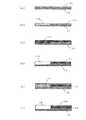
図1〜図5は、本発明の一実施の形態を示し、図1は平面図、図2は図1のA−A線断面図、図3は、図1のB−B線断面図、図4は図1のC−C線断面図である。 1 to 5 show an embodiment of the present invention, FIG. 1 is a plan view, FIG. 2 is a sectional view taken along line AA in FIG. 1, and FIG. 3 is a sectional view taken along line BB in FIG. 4 is a cross-sectional view taken along the line CC of FIG.
図において、10は、ガラエポ基板、ガラス、プラスチック板等からなる支持基板で、その支持基板10上の中央から一辺(図では右辺)に向けて複数のコア11とクラッド12からなるポリマ導波路13が形成され、そのポリマ導波路13を形成するコア材とクラッド材を用いて支持基板10上の中央から他辺(左辺)にかけて凸状の位置合わせ用パターン14が複数本形成され、その位置合わせ用パターン14間で光ファイバガイド溝15が形成される。 In the figure,
この光ファイバガイド溝15に図7、図8に示すように光ファイバ20が実装され、また光ファイバ20とポリマ導波路13を接着剤23により接着して光配線基板30を形成する。 The
この接着は、ポリマ導波路13のコア11の屈折率とファイバコア21の屈折率の間の屈折率を持つ接着剤23を用い、また接着剤23で、光ファイバ20のクラッド22も、光ファイバガイド溝15を形成する支持基板10と位置合わせ用パターン14に接着固定する。 For this bonding, an adhesive 23 having a refractive index between the refractive index of the
図5、図6は、支持基板10上にポリマ導波路13と位置合わせ用パターン14とを同時に形成する工程を示したものである。 FIGS. 5 and 6 show a process of simultaneously forming the
先ず、図5(a)に示すように、支持基板10上にアンダークラッド材(アクリル系紫外線硬化樹脂、屈折率1.51)12uが塗布され、ポリマ導波路と位置合わせ用パターンの形状を形成したマスク(図示せず)にてUV露光されて硬化され、未露光・未硬化部分が現像液(アセトン)で除去されて、図5(b)、図6(b)に示すようにポリマ導波路13のアンダークラッド12bと位置合わせ用パターン14bが形成される。 First, as shown in FIG. 5 (a), an undercladding material (acrylic ultraviolet curable resin, refractive index 1.51) 12u is applied on the
このアンダークラッド12bの厚さは、上述した光ファイバ20のクラッド22の厚さと同じになるように形成する。 The thickness of the under
次に図5(c)に示すように、コア材(アクリル系紫外線硬化樹脂、屈折率1.56)11cが塗布され、ポリマ導波路のコアと位置合わせ用パターンの形状を形成したマスク(図示せず)にてUV露光されて硬化され、未露光・未硬化部分が現像液で除去されて、図5(d)、図6(d)に示すようにポリマ導波路13のコア11と位置合わせ用パターン14dが形成される。 Next, as shown in FIG. 5 (c), a core material (acrylic ultraviolet curable resin, refractive index 1.56) 11c is applied to form a mask having a shape of a pattern for alignment with the core of the polymer waveguide (FIG. 5C). (Not shown) is UV-exposed and cured, and unexposed / uncured portions are removed with a developer, and the
このコア11の厚さと幅は、光ファイバ20のコア径と同じになるよう形成する。 The
さらに、図5(e)に示すようにオーバクラッド材11oが塗布され、ポリマ導波路と位置合わせ用パターンの形状を形成したマスク(図示せず)にてUV露光されて硬化され、未露光・未硬化部分が現像液で除去されて、図5(f)に示すようにオーバークラッド12fが形成されて、図1に示したポリマ導波路13と位置合わせ用パターン14が形成される。 Furthermore, as shown in FIG. 5 (e), an overcladding material 11o is applied, UV-exposed with a mask (not shown) in the shape of the alignment pattern of the polymer waveguide and cured, and unexposed / The uncured portion is removed with a developing solution to form an overclad 12f as shown in FIG. 5F, and the
この支持基板10へのポリマ導波路13と位置合わせ用パターン14は、図示のように予め使用する形状に形成しても、或いは大きな支持基板10を用い、その支持基板10上に、ポリマ導波路13と位置合わせ用パターン14を多数形成した後、ダイシングにより図示した四角形状に切り出して形成するようにしてもよい。 The
以上のように支持基板10へのポリマ導波路13と位置合わせ用パターン14を形成した後、図7、図8で説明したように光ファイバ20を位置合わせ用パターン14間の光ファイバガイド溝15に実装して、光ファイバ20のコア21とポリマ導波路13のコア11とを結合する。この場合、支持基板10からコア11の中心までの高さは、光ファイバ20の半径と同じに形成され、また位置合わせ用パターン14は、マスクを用いて露光・現像して形成するため、精密である、光ファイバガイド溝15に光ファイバ20を嵌め込めば、光ファイバ20のコア21とポリマ導波路13のコア11との調心ができる。 After the
この光ファイバ20は、コア径が数10μmのマルチモードファイバであり、クラッド22の径の誤差は、サブミクロン程度であり、上述のように位置合わせ用パターン14をマスクを用いて露光・現像して形成することで、接続のための調心作業を必要とせず、低コスト化が可能となる。 The
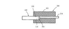
次に、この光配線基板30を用いて、光モジュールを構成する例を図9、図10により説明する。 Next, an example in which an optical module is configured using the
図9に示すように、サブマウントコネクタ32には、光配線基板30のポリマ導波路13を挿入する挿入穴33が形成され、また、ポリマ導波路13のコア11(図示なし)に位置してファイバーアレー34が形成されており、その挿入穴33に光配線基板30を挿入し、接着剤35で固定することで光モジュール36とすることができる。 As shown in FIG. 9, the
図10は、光配線基板と光素子とを結合した光モジュール40の例を示したものである。 FIG. 10 shows an example of an
透明なサブマウントコネクタ41には、光配線基板30のポリマ導波路13を挿入する挿入穴42が形成され、その挿入穴42内に光路を垂直に変換するミラー43が設けられ、サブマウントコネクタ41に、そのミラー43に位置してVCSELアレイやPDアレイなどの光素子44がハンダ45で実装される。 The transparent
このミラー43は、プリズム状をしたガラスで作製されており、反射面に金属コート、または多層膜コートが施されている。 The
サブマウントコネクタ41の挿入穴42内のミラー43と結合するよう光配線基板30のポリマ導波路13を挿入すると共に接着剤46で固定して光モジュール40とする。 The
この光モジュール40においては、VCSELアレイからなる光素子44からの光信号がサブマウントコネクタ41を通し、ミラー43で全反射されて光配線基板30のポリマ導波路13の各コアに入射され、光ファイバ20(図示せず)に送信される。また光素子44がPDアレイの場合、光ファイバ20からの光信号がポリマ導波路13からミラー43に入射され、ミラー43で全反射されて光素子44で受信される。 In this
図11は、光配線基板30の変形例を示したもので、支持基板10上に、ポリマ導波路13と位置合わせ用パターン14(図示なし)を形成する他にクラッド12の部分をやや大きめに形成し、その余剰のクラッド部分12sに他の光部品との位置合わせ用の溝47を形成したもので、これにより光配線基板30を他の光部品に取り付ける際の位置決め精度を向上させることができる。 FIG. 11 shows a modified example of the
なお、上述の実施の形態では、紫外線硬化樹脂を塗布し、これを露光し、現像液で未硬化部分を除去する例で説明したが、位置合わせ用パターン14の形成には、この他にも、支持基板10やクラッド12をエッチングにより形成するようにしてもよい。またこのエッチングは大きめにしてラフでよく、精密なエッチングはコア加工のときに行えばよい。 In the above-described embodiment, an example in which an ultraviolet curable resin is applied, exposed, and uncured portions are removed with a developer has been described. However, the
10 支持基板
11 コア
12 クラッド
13 ポリマ導波路
14 位置合わせ用パターン
15 光ファイバガイド溝
20 光ファイバ
DESCRIPTION OF
Claims (5)
Translated fromJapaneseThe optical wiring board according to any one of claims 1 to 3 is inserted into the insertion hole of the submount connector, and a mirror for vertically converting the optical path is provided in the insertion hole. An optical module in which an element is mounted.
Priority Applications (1)
| Application Number | Priority Date | Filing Date | Title |
|---|---|---|---|
| JP2005379101AJP2007178852A (en) | 2005-12-28 | 2005-12-28 | Optical wiring board and optical module using the same |
Applications Claiming Priority (1)
| Application Number | Priority Date | Filing Date | Title |
|---|---|---|---|
| JP2005379101AJP2007178852A (en) | 2005-12-28 | 2005-12-28 | Optical wiring board and optical module using the same |
Publications (1)
| Publication Number | Publication Date |
|---|---|
| JP2007178852Atrue JP2007178852A (en) | 2007-07-12 |
Family
ID=38304084
Family Applications (1)
| Application Number | Title | Priority Date | Filing Date |
|---|---|---|---|
| JP2005379101APendingJP2007178852A (en) | 2005-12-28 | 2005-12-28 | Optical wiring board and optical module using the same |
Country Status (1)
| Country | Link |
|---|---|
| JP (1) | JP2007178852A (en) |
Cited By (10)
| Publication number | Priority date | Publication date | Assignee | Title |
|---|---|---|---|---|
| JP2009198803A (en)* | 2008-02-21 | 2009-09-03 | Sony Corp | Optical module and optical waveguide |
| JP2012113031A (en)* | 2010-11-22 | 2012-06-14 | Hitachi Chem Co Ltd | Optical fiber connector and method of manufacturing the same |
| JP2012128271A (en)* | 2010-12-16 | 2012-07-05 | Hitachi Chem Co Ltd | Optical fiber connector |
| JP2012133235A (en)* | 2010-12-22 | 2012-07-12 | Hitachi Chem Co Ltd | Optical fiber connector and manufacturing method therefor |
| JP2012155191A (en)* | 2011-01-27 | 2012-08-16 | Hitachi Chem Co Ltd | Optical fiber connector and method for manufacturing the same |
| JP2012155192A (en)* | 2011-01-27 | 2012-08-16 | Hitachi Chem Co Ltd | Optical fiber connector and method for manufacturing the same |
| JP2012163714A (en)* | 2011-02-04 | 2012-08-30 | Hitachi Chem Co Ltd | Optical fiber connector and manufacturing method therefor |
| JP2016071256A (en)* | 2014-09-30 | 2016-05-09 | 住友大阪セメント株式会社 | Optical modulator |
| WO2016180071A1 (en)* | 2015-05-08 | 2016-11-17 | 中兴通讯股份有限公司 | Coupled connecting method for optical wave guide plate and optical fibers, optical wave guide plate and telecommunication transmission system |
| US11415753B2 (en) | 2020-04-30 | 2022-08-16 | Corning Research & Development Corporation | High-density FAUs and optical interconnection devices and related methods |
- 2005
- 2005-12-28JPJP2005379101Apatent/JP2007178852A/enactivePending
Cited By (15)
| Publication number | Priority date | Publication date | Assignee | Title |
|---|---|---|---|---|
| JP2009198803A (en)* | 2008-02-21 | 2009-09-03 | Sony Corp | Optical module and optical waveguide |
| US8180189B2 (en) | 2008-02-21 | 2012-05-15 | Sony Corporation | Optical module and optical waveguide |
| JP2012113031A (en)* | 2010-11-22 | 2012-06-14 | Hitachi Chem Co Ltd | Optical fiber connector and method of manufacturing the same |
| JP2012128271A (en)* | 2010-12-16 | 2012-07-05 | Hitachi Chem Co Ltd | Optical fiber connector |
| JP2012133235A (en)* | 2010-12-22 | 2012-07-12 | Hitachi Chem Co Ltd | Optical fiber connector and manufacturing method therefor |
| JP2012155191A (en)* | 2011-01-27 | 2012-08-16 | Hitachi Chem Co Ltd | Optical fiber connector and method for manufacturing the same |
| JP2012155192A (en)* | 2011-01-27 | 2012-08-16 | Hitachi Chem Co Ltd | Optical fiber connector and method for manufacturing the same |
| JP2012163714A (en)* | 2011-02-04 | 2012-08-30 | Hitachi Chem Co Ltd | Optical fiber connector and manufacturing method therefor |
| JP2016071256A (en)* | 2014-09-30 | 2016-05-09 | 住友大阪セメント株式会社 | Optical modulator |
| WO2016180071A1 (en)* | 2015-05-08 | 2016-11-17 | 中兴通讯股份有限公司 | Coupled connecting method for optical wave guide plate and optical fibers, optical wave guide plate and telecommunication transmission system |
| US11415753B2 (en) | 2020-04-30 | 2022-08-16 | Corning Research & Development Corporation | High-density FAUs and optical interconnection devices and related methods |
| US11567285B2 (en) | 2020-04-30 | 2023-01-31 | Corning Research & Development Corporation | High-density FAUs and optical interconnection devices including optimized arrays and related methods |
| US11586000B2 (en) | 2020-04-30 | 2023-02-21 | Corning Research & Development Corporation | High-density FAUs and optical interconnection devices and related methods |
| US11828998B2 (en) | 2020-04-30 | 2023-11-28 | Corning Research & Development Corporation | High-density FAUs and optical interconnection devices and related methods |
| US11934025B2 (en) | 2020-04-30 | 2024-03-19 | Corning Research & Development Corporation | FAUs including passive alignment adhesive profiles and related methods |
Similar Documents
| Publication | Publication Date | Title |
|---|---|---|
| US10684419B2 (en) | Waveguide connector elements and optical assemblies incorporating the same | |
| JP4577376B2 (en) | Manufacturing method of optical waveguide | |
| US7362934B2 (en) | Optical connecting device and connector | |
| JP4730274B2 (en) | Optical coupler, optical connector, and receptacle type optical transmission module | |
| JP4910788B2 (en) | Optical module and optical waveguide manufacturing method | |
| US20080138007A1 (en) | Optical waveguide and optical module using the same | |
| JP2009198804A (en) | Optical module and optical waveguide | |
| US20190121030A1 (en) | Optical coupler for coupling light in/out of an optical receiving/emitting structure | |
| CN112305678B (en) | Optical connector | |
| JP2016071137A (en) | Waveguide connector and alignment method | |
| JP2007178852A (en) | Optical wiring board and optical module using the same | |
| JP4349372B2 (en) | Optical module and optical module manufacturing method | |
| JP4752092B2 (en) | Optical waveguide connection structure and optical element mounting structure | |
| JP2014029386A (en) | Method for producing polymer waveguide array assembly of single mode | |
| JP2007072007A (en) | Optical waveguide module | |
| Palen | Low cost optical interconnects | |
| JP2007183467A (en) | Optical waveguide with mirror and manufacturing method thereof | |
| JP2010066474A (en) | Optical connection structure | |
| WO2007080740A1 (en) | Optical waveguide device and device for producing optical waveguide device | |
| EP2031427B1 (en) | Optical terminal | |
| JP4692424B2 (en) | Waveguide array for multicore bidirectional communication, method for manufacturing the same, and bidirectional communication module | |
| JP4565076B2 (en) | Optical path conversion device, optical transmission device manufacturing method, and manufacturing tool therefor | |
| JP4524390B2 (en) | Manufacturing method of optical connection device | |
| JP5686015B2 (en) | Optical connector and optical connector manufacturing method | |
| JP2010286549A (en) | Light signal processing circuit, semiconductor device with the light signal processing circuit, and method of manufacturing the light signal processing circuit |