JP2007165431A - Field effect transistor and manufacturing method thereof - Google Patents
Field effect transistor and manufacturing method thereofDownload PDFInfo
- Publication number
- JP2007165431A JP2007165431AJP2005357240AJP2005357240AJP2007165431AJP 2007165431 AJP2007165431 AJP 2007165431AJP 2005357240 AJP2005357240 AJP 2005357240AJP 2005357240 AJP2005357240 AJP 2005357240AJP 2007165431 AJP2007165431 AJP 2007165431A
- Authority
- JP
- Japan
- Prior art keywords
- layer
- forming
- barrier layer
- gan
- insulating film
- Prior art date
- Legal status (The legal status is an assumption and is not a legal conclusion. Google has not performed a legal analysis and makes no representation as to the accuracy of the status listed.)
- Pending
Links
Images


Landscapes
- Junction Field-Effect Transistors (AREA)
- Thin Film Transistor (AREA)
Abstract
Description
Translated fromJapanese本発明は窒化物半導体から構成されたヘテロ構造を用いた電界効果型トランジスタおよびその製造方法に関するものである。 The present invention relates to a field effect transistor using a heterostructure composed of a nitride semiconductor and a method for manufacturing the same.
GaNをはじめとした窒化物半導体は、高い絶縁破壊電界強度、高い熱伝導率および高い電子飽和速度等の特性を有しており、高周波のハイパワーデバイス向けの材料として優れている。例えば、サファイア基板上にGaNからなる電子走行層(バッファ層)およびAlGaNからなるバリア層を有するヘテロ接合構造においては、ヘテロ接合界面近傍に電子が高濃度に蓄積され、いわゆる2次元電子ガス(2DEG)を形成する。この2次元電子ガスは散乱要因となる導電性不純物が存在しないアンドープGaNからなる電子走行層内を走行できるために高い電子移動度を示し、いわゆる高電子移動度トランジスタ(HEMT)として動作させることが可能である。 Nitride semiconductors such as GaN have characteristics such as high breakdown field strength, high thermal conductivity, and high electron saturation speed, and are excellent materials for high-frequency high-power devices. For example, in a heterojunction structure having an electron transit layer (buffer layer) made of GaN and a barrier layer made of AlGaN on a sapphire substrate, electrons are accumulated at a high concentration near the heterojunction interface, so-called two-dimensional electron gas (2DEG ). Since this two-dimensional electron gas can travel in an electron transit layer made of undoped GaN free of conductive impurities that cause scattering, it exhibits high electron mobility and can be operated as a so-called high electron mobility transistor (HEMT). Is possible.
上に述べた例をはじめ、窒化物半導体から構成される高電子移動度トランジスタでは、AlGaN層をバリア層として用いることが多い。これは、AlGaN層の形成が比較的容易であること、AlGaN層のAl組成、層厚を変化させることにより、2次元電子ガスのシートキャリア濃度を制御できることなど、デバイス製造上、設計上のフレキシビリティがあるためである。 In the high electron mobility transistor including a nitride semiconductor including the example described above, an AlGaN layer is often used as a barrier layer. This is because it is relatively easy to form an AlGaN layer, and the sheet carrier concentration of the two-dimensional electron gas can be controlled by changing the Al composition and thickness of the AlGaN layer. This is because there is a possibility.
しかし、AlGaNからなるバリア層を有する高電子移動度トランジスタでは、AlGaNとGaNとの格子不整合により、特にAl組成が高くなるにつれて形成できるAlGaN層厚範囲が狭くなり、2次元電子ガスのシートキャリア濃度について十分広範囲な設計余裕を確保できない、という難点もあった。こうした難点を解決するために、バリア層の材料としてInAlNを用いた高電子移動度トランジスタが提案されている。 However, in a high electron mobility transistor having a barrier layer made of AlGaN, the AlGaN layer thickness range that can be formed becomes narrower as the Al composition becomes higher due to lattice mismatch between AlGaN and GaN, and the sheet carrier of the two-dimensional electron gas. There was also a problem that a sufficiently wide design margin could not be secured for the concentration. In order to solve these difficulties, a high electron mobility transistor using InAlN as a material for the barrier layer has been proposed.
InAlNはIn組成0.17においてGaNと格子整合するため、InAlNをバリア層に用いると、バリア層厚に対する制限がAlGaNをバリア層に用いた場合よりも格段に緩和される。また、In組成0.17におけるInAlNのエネルギー禁制帯幅はおよそ4.9eVで、AlGaNからなるバリア層を有する高電子移動度トランジスタで通常用いられるAl組成範囲(典型的には0.1〜0.3)でのAlGaNのエネルギー禁制帯幅(3.7〜4.2eV)より大きい。また、In組成0.17であるInAlNとGaNとのヘテロ接合界面に存在する伝導電子帯におけるエネルギー障壁△Ecは0.7eV程度あり、AlGaNからなるバリア層を有する高電子移動度トランジスタにおけるAlGaNとGaNとのヘテロ界面に存在するエネルギー障壁△Ec(0.1〜0.3eV程度)よりも大きい。さらに、InAlNはAlGaNに比べて自発分極効果が大きい。これらの特徴から、InAlNをバリア層とする高電子移動度トランジスタではAlGaNをバリア層とする高電子移動度トランジスタよりも2次元電子ガスのシートキャリア濃度を高くすることができるという優れた特性を有する。 Since InAlN lattice matches with GaN with an In composition of 0.17, when InAlN is used for the barrier layer, the restriction on the barrier layer thickness is remarkably relaxed than when AlGaN is used for the barrier layer. InAlN having an In composition of 0.17 has an energy forbidden band width of about 4.9 eV, and is an Al composition range (typically 0.1 to 0 typically used in a high electron mobility transistor having a barrier layer made of AlGaN. .3) larger than the energy forbidden band width of AlGaN (3.7 to 4.2 eV). Further, the energy barrier ΔEc in the conduction electron band existing at the heterojunction interface between InAlN and GaN having an In composition of 0.17 is about 0.7 eV, and AlGaN in a high electron mobility transistor having a barrier layer made of AlGaN It is larger than the energy barrier ΔEc (about 0.1 to 0.3 eV) existing at the heterointerface with GaN. Furthermore, InAlN has a greater spontaneous polarization effect than AlGaN. From these characteristics, the high electron mobility transistor using InAlN as a barrier layer has an excellent characteristic that the sheet carrier concentration of the two-dimensional electron gas can be made higher than the high electron mobility transistor using AlGaN as a barrier layer. .
加えて、InAlNのエネルギー禁制帯幅が大きく、かつ伝導電子帯におけるエネルギー障壁が高いという特徴は、バリア層上にゲート電極を形成した場合にゲートリーク電流を低減させ、かつゲート耐圧を向上させることを可能とする。 In addition, InAlN has a large energy forbidden band width and a high energy barrier in the conduction electron band. When the gate electrode is formed on the barrier layer, the gate leakage current is reduced and the gate breakdown voltage is improved. Is possible.
図9はInAlNをバリア層とするInAlN/GaNヘテロ構造を用いた従来の電界効果型トランジスタ(高電子移動度トランジスタ)を示す断面図である。図に示すように、基板1上にGaNからなる電子走行層2が形成され、電子走行層2上にInAlNからなるバリア層3が形成され、バリア層3の上面にはゲート電極4が形成され、ゲート電極4の両側にソース電極5およびドレイン電極6が形成されている。 FIG. 9 is a sectional view showing a conventional field effect transistor (high electron mobility transistor) using an InAlN / GaN heterostructure having InAlN as a barrier layer. As shown in the figure, an
この電界効果型トランジスタにおいては、電子走行層2とバリア層3とのヘテロ界面近傍に高濃度の2次元電子ガス7が形成され、ゲート電極4に印加する電圧によって2次元電子ガスのシートキャリア濃度を制御することによりトランジスタとしての動作が実現される。このため、窒化物半導体を用いた電界効果型トランジスタでは、バリア層3の厚さが非常に薄く(典型的には数nm〜数十nm)、2次元電子ガス7とゲート電極4とは空間的に近接する構造となる。したがって、バリア層3が2次元電子ガス7とゲート電極4との間に対して十分なエネルギー障壁を持たない場合には、ゲートリーク電流が発生して十分なゲート耐圧が得られず、良好な素子特性が得られなくなってしまうが、エネルギー禁制帯幅が大きく、かつ伝導電子帯におけるエネルギー障壁が高いInAlNをバリア層3に用いることで、バリア層3の厚さが極薄であってもゲートリーク電流を抑制しゲート耐圧を向上させることが可能となる。 In this field effect transistor, a high-concentration two-
上述したように、バリア層3をInAlNで構成することは、ゲートリーク電流の低減、ゲート耐圧の向上という観点では有利であるが、ソースおよびドレインのコンタクト抵抗の低減という観点からは不利となる。すなわち、図9に示した従来の電界効果型トランジスタにおいては、ソース電極5およびドレイン電極6もバリア層3上に形成しているから、ソース電極5とドレイン電極6との間に高いエネルギー障壁が存在することになり、ソースおよびドレインのコンタクト抵抗を増大させてしまう。 As described above, configuring the
本発明は上述の課題を解決するためになされたもので、良好なゲート耐圧特性を有し、かつソースおよびドレインのコンタクト抵抗が小さい電界効果型トランジスタ、その製造方法を提供することを目的とする。 The present invention has been made to solve the above-described problems, and an object of the present invention is to provide a field effect transistor having good gate breakdown voltage characteristics and low source and drain contact resistance, and a method for manufacturing the same. .
この目的を達成するため、本発明においては、基板上に形成されたGaNからなる電子走行層と、前記電子走行層上に形成されたInAlNからなるバリア層と、前記バリア層上に形成されたゲート電極と、前記ゲート電極の両側に形成されたソース電極およびドレイン電極とを有する電界効果型トランジスタにおいて、前記ソース電極および前記ドレイン電極と前記バリア層との間にInGaN、InN、GaNの少なくとも1つからなるキャップ層を形成する。 In order to achieve this object, in the present invention, an electron transit layer made of GaN formed on a substrate, a barrier layer made of InAlN formed on the electron transit layer, and formed on the barrier layer. In a field effect transistor having a gate electrode and a source electrode and a drain electrode formed on both sides of the gate electrode, at least one of InGaN, InN, and GaN is provided between the source electrode and the drain electrode and the barrier layer. A cap layer made of one is formed.
また、基板上に形成されたGaNからなる電子走行層と、前記電子走行層上に形成されたInAlNからなるバリア層と、前記バリア層上に形成されたゲート電極と、前記ゲート電極の両側に形成されたソース電極およびドレイン電極とを有する電界効果型トランジスタにおいて、前記ソース電極および前記ドレイン電極と前記電子走行層との間にn型のInGaN、InN、GaNの少なくとも1つからなるキャップ層を形成する。 Further, an electron transit layer made of GaN formed on the substrate, a barrier layer made of InAlN formed on the electron transit layer, a gate electrode formed on the barrier layer, and on both sides of the gate electrode In the field effect transistor having the formed source electrode and drain electrode, a cap layer made of at least one of n-type InGaN, InN, and GaN is provided between the source and drain electrodes and the electron transit layer. Form.
これらの場合、前記バリア層と前記ゲート電極との間に絶縁膜を形成してもよい。 In these cases, an insulating film may be formed between the barrier layer and the gate electrode.
これらの場合、前記電子走行層と前記バリア層との間にAlN層を形成してもよい。 In these cases, an AlN layer may be formed between the electron transit layer and the barrier layer.
これらの場合、前記電子走行層と前記バリア層との間に、InGaN層、InGaN層およびAlN層またはInGaN層およびGaN層を形成してもよい。 In these cases, an InGaN layer, an InGaN layer and an AlN layer, or an InGaN layer and a GaN layer may be formed between the electron transit layer and the barrier layer.
また、電界効果型トランジスタの製造方法において、基板上にGaNからなる電子走行層を形成する工程と、前記電子走行層上にInAlNからなるバリア層を形成する工程と、前記バリア層上にInGaN、InN、GaNの少なくとも1つからなるキャップ層を形成する工程と、前記キャップ層のゲート電極を形成する領域を除去する工程と、前記バリア層上に前記ゲート電極を形成する工程と、前記キャップ層上にソース電極およびドレイン電極を形成する工程とを行なう。 Further, in the method of manufacturing a field effect transistor, a step of forming an electron transit layer made of GaN on a substrate, a step of forming a barrier layer made of InAlN on the electron transit layer, InGaN on the barrier layer, A step of forming a cap layer made of at least one of InN and GaN, a step of removing a region for forming a gate electrode of the cap layer, a step of forming the gate electrode on the barrier layer, and the cap layer Forming a source electrode and a drain electrode thereon.
また、電界効果型トランジスタの製造方法において、基板上にGaNからなる電子走行層を形成する工程と、前記電子走行層上にInAlNからなるバリア層を形成する工程と、前記バリア層上にInGaN、InN、GaNの少なくとも1つからなるキャップ層を形成する工程と、前記キャップ層のゲート電極を形成する領域を除去する工程と、前記キャップ層を除去した領域に絶縁膜を形成する工程と、前記絶縁膜上に前記ゲート電極を形成する工程と、前記キャップ層上にソース電極およびドレイン電極を形成する工程とを行なう。 Further, in the method of manufacturing a field effect transistor, a step of forming an electron transit layer made of GaN on a substrate, a step of forming a barrier layer made of InAlN on the electron transit layer, InGaN on the barrier layer, A step of forming a cap layer made of at least one of InN and GaN, a step of removing a region where the gate electrode of the cap layer is formed, a step of forming an insulating film in the region where the cap layer is removed, A step of forming the gate electrode on the insulating film and a step of forming a source electrode and a drain electrode on the cap layer are performed.
また、電界効果型トランジスタの製造方法において、基板上にGaNからなる電子走行層を形成する工程と、前記電子走行層上にInAlNからなるバリア層を形成する工程と、前記バリア層上に絶縁膜を形成する工程と、前記絶縁膜のソース電極およびドレイン電極を形成する領域を除去する工程と、前記絶縁膜を除去した領域にInGaN、InN、GaNの少なくとも1つからなるキャップ層を形成する工程と、前記絶縁膜を除去する工程と、前記バリア層上に前記ゲート電極を形成する工程と、前記キャップ層上に前記ソース電極および前記ドレイン電極を形成する工程とを行なう。 Further, in the method of manufacturing a field effect transistor, a step of forming an electron transit layer made of GaN on a substrate, a step of forming a barrier layer made of InAlN on the electron transit layer, and an insulating film on the barrier layer A step of forming a source electrode and a drain electrode of the insulating film, and a step of forming a cap layer made of at least one of InGaN, InN, and GaN in the region from which the insulating film has been removed. And a step of removing the insulating film, a step of forming the gate electrode on the barrier layer, and a step of forming the source electrode and the drain electrode on the cap layer.
また、電界効果型トランジスタの製造方法において、基板上にGaNからなる電子走行層を形成する工程と、前記電子走行層上にInAlNからなるバリア層を形成する工程と、前記バリア層上に絶縁膜を形成する工程と、前記絶縁膜のソース電極およびドレイン電極を形成する領域を除去する工程と、前記絶縁膜を除去した領域にInGaN、InN、GaNの少なくとも1つからなるキャップ層を形成する工程と、前記絶縁膜上に前記ゲート電極を形成する工程と、前記キャップ層上に前記ソース電極および前記ドレイン電極を形成する工程とを行なう。 Further, in the method of manufacturing a field effect transistor, a step of forming an electron transit layer made of GaN on a substrate, a step of forming a barrier layer made of InAlN on the electron transit layer, and an insulating film on the barrier layer A step of forming a source electrode and a drain electrode of the insulating film, and a step of forming a cap layer made of at least one of InGaN, InN, and GaN in the region from which the insulating film has been removed. And a step of forming the gate electrode on the insulating film and a step of forming the source electrode and the drain electrode on the cap layer.
また、電界効果型トランジスタの製造方法において、基板上にGaNからなる電子走行層を形成する工程と、前記電子走行層上にInAlNからなるバリア層を形成する工程と、前記バリア層上に絶縁膜を形成する工程と、前記絶縁膜のソース電極およびドレイン電極を形成する領域を除去する工程と、前記絶縁膜を除去した領域の前記バリア層を除去する工程と、前記バリア層を除去した領域の前記電子走行層の一部を除去する工程と、前記電子走行層の一部を除去した領域にn型のInGaN、InN、GaNの少なくとも1つからなるキャップ層を形成する工程と、前記絶縁膜を除去する工程と、前記バリア層上にゲート電極を形成する工程と、前記キャップ層上に前記ソース電極および前記ドレイン電極を形成する工程とを行なう。 Further, in the method of manufacturing a field effect transistor, a step of forming an electron transit layer made of GaN on a substrate, a step of forming a barrier layer made of InAlN on the electron transit layer, and an insulating film on the barrier layer Forming a source electrode and a drain electrode in the insulating film, removing the barrier layer in the region from which the insulating film has been removed, and removing the barrier layer in the region from which the barrier layer has been removed. Removing a part of the electron transit layer, forming a cap layer made of at least one of n-type InGaN, InN, and GaN in a region from which a part of the electron transit layer is removed, and the insulating film A step of forming a gate electrode on the barrier layer, and a step of forming the source electrode and the drain electrode on the cap layer.
また、電界効果型トランジスタの製造方法において、基板上にGaNからなる電子走行層を形成する工程と、前記電子走行層上にInAlNからなるバリア層を形成する工程と、前記バリア層上に絶縁膜を形成する工程と、前記絶縁膜のソース電極およびドレイン電極を形成する領域を除去する工程と、前記絶縁膜を除去した領域の前記バリア層を除去する工程と、前記バリア層を除去した領域の前記電子走行層の一部を除去する工程と、前記電子走行層の一部を除去した領域にn型のInGaN、InN、GaNの少なくとも1つからなるキャップ層を形成する工程と、前記絶縁膜上にゲート電極を形成する工程と、前記キャップ層上に前記ソース電極および前記ドレイン電極を形成する工程とを行なう。 Further, in the method of manufacturing a field effect transistor, a step of forming an electron transit layer made of GaN on a substrate, a step of forming a barrier layer made of InAlN on the electron transit layer, and an insulating film on the barrier layer Forming a source electrode and a drain electrode in the insulating film, removing the barrier layer in the region from which the insulating film has been removed, and removing the barrier layer in the region from which the barrier layer has been removed. Removing a part of the electron transit layer, forming a cap layer made of at least one of n-type InGaN, InN, and GaN in a region from which a part of the electron transit layer is removed, and the insulating film A step of forming a gate electrode thereon and a step of forming the source electrode and the drain electrode on the cap layer are performed.
本発明に係る電界効果型トランジスタ、その製造方法においては、InAlNからなるバリア層を形成しているから、エネルギー障壁を高くすることができるので、ゲート耐圧特性を良好にすることができ、またソース電極およびドレイン電極とInAlNからなるバリア層との間にInGaN、InN、GaNの少なくとも1つからなるキャップ層を形成しているから、ソースおよびドレインのコンタクト抵抗を小さくすることができる。 In the field effect transistor and the manufacturing method thereof according to the present invention, since the barrier layer made of InAlN is formed, the energy barrier can be increased, so that the gate breakdown voltage characteristic can be improved, and the source Since the cap layer made of at least one of InGaN, InN, and GaN is formed between the electrode and drain electrode and the barrier layer made of InAlN, the contact resistance of the source and drain can be reduced.
また、本発明に係る他の電界効果型トランジスタ、その製造方法においては、InAlNからなるバリア層を形成しているから、エネルギー障壁を高くすることができるので、ゲート耐圧特性を良好にすることができ、またソース電極およびドレイン電極と電子走行層との間にn型のInGaN、InN、GaNの少なくとも1つからなるキャップ層を形成しているから、ソース電極およびドレイン電極を形成する領域にはバリア層が存在しないので、ソースおよびドレインのコンタクト抵抗を低減することができるとともに、ソースおよびドレインの寄生抵抗成分も低減することができる。 In addition, in another field effect transistor according to the present invention and its manufacturing method, since the barrier layer made of InAlN is formed, the energy barrier can be increased, so that the gate breakdown voltage characteristics can be improved. In addition, since a cap layer made of at least one of n-type InGaN, InN, and GaN is formed between the source and drain electrodes and the electron transit layer, the region where the source and drain electrodes are formed Since the barrier layer is not present, the source and drain contact resistance can be reduced, and the parasitic resistance components of the source and drain can be reduced.
また、バリア層とゲート電極との間に絶縁膜を形成したときには、ゲートリーク電流を確実に低減することができる。 Further, when an insulating film is formed between the barrier layer and the gate electrode, the gate leakage current can be reliably reduced.
また、電子走行層とバリア層との間にAlN層を形成したときには、ゲートリーク電流を確実に低減することができ、また電子移動度およびシートキャリア濃度を高くすることができる。 Further, when an AlN layer is formed between the electron transit layer and the barrier layer, the gate leakage current can be reliably reduced, and the electron mobility and the sheet carrier concentration can be increased.
また、電子走行層とバリア層との間に、InGaN層、InGaN層およびAlN層またはInGaN層およびGaN層を形成したときには、電子移動度を高くすることができる。 Further, when an InGaN layer, an InGaN layer, and an AlN layer or an InGaN layer and a GaN layer are formed between the electron transit layer and the barrier layer, the electron mobility can be increased.
(第1の実施の形態)
図1は本発明における第1の実施の形態の電界効果型トランジスタを示す断面図である。図に示すように、サファイアからなる基板11上にGaNからなる電子走行層12が形成され、電子走行層12上にInAlNからなるバリア層13が形成され、バリア層13上にゲート電極15が形成され、バリア層13のゲート電極15の両側の領域上にInGaN、InN、GaNの少なくとも1つからなるキャップ層14が形成され、キャップ層14上にソース電極16およびドレイン電極17が形成されている。すなわち、ゲート電極15の両側にソース電極16およびドレイン電極17が形成され、ソース電極16およびドレイン電極17とバリア層13との間にキャップ層14が形成されている。(First embodiment)
FIG. 1 is a sectional view showing a field effect transistor according to a first embodiment of the present invention. As shown in the figure, an
この電界効果型トランジスタにおいては、InAlNからなるバリア層13を有しているから、エネルギー障壁を高くすることができるので、ゲートリーク電流を低減することができ、ゲート耐圧を向上することができる。さらに、ソース電極16およびドレイン電極17とInAlNからなるバリア層13との間にInGaN、InN、GaNの少なくとも1つからなるキャップ層14が形成されているから、ソースおよびドレインのコンタクト抵抗を小さくすることができる。すなわち、オーミック電極と半導体材料との間のエネルギー障壁の高さは、オーミック電極を形成する金属材料の仕事関数と半導体材料の電子親和力とによって決まるが、本質的にエネルギー禁制帯幅の小さい半導体材料ほど電子親和力が大きくなり、結果的にエネルギー障壁を小さくすることができる。したがって、InAlNよりもエネルギー禁制帯幅を小さくできるInGaN、InN、GaNの少なくとも1つからなるキャップ層14をソース電極16およびドレイン電極17と接する部分に形成することによって、ソース電極16およびドレイン電極17を構成する金属材料とのエネルギー障壁を小さくすることができるから、ソースおよびドレインのコンタクト抵抗を小さくすることができる。 Since this field effect transistor has the
なお、バリア層13とゲート電極15との間にGaN、InAlN、InGaN、InNよりも大きいエネルギー禁制帯幅を有する絶縁膜(AlNを含む)を形成してもよい。この場合、ゲートリーク電流を確実に低減することができる。 Note that an insulating film (including AlN) having a larger energy forbidden band than GaN, InAlN, InGaN, and InN may be formed between the
また、電子走行層12とバリア層13との間にAlN層を形成してもよい。この場合、ゲートリーク電流を確実に低減することができ、また電子移動度およびシートキャリア濃度を高くすることができる。 Further, an AlN layer may be formed between the
また、電子走行層12とバリア層13との間に、InGaN層、InGaN層およびAlN層またはInGaN層およびGaN層を形成してもよい。この場合、電子移動度を高くすることができる。 Further, an InGaN layer, an InGaN layer and an AlN layer, or an InGaN layer and a GaN layer may be formed between the
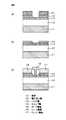
つぎに、図2、図3により図1に示した電界効果型トランジスタの製造方法、すなわち本発明に係る電界効果型トランジスタの製造方法を説明する。まず、図2(a)、(b)に示すように、サファイアからなる基板11上にノンドープGaNからなる電子走行層12を層厚2μm程度成長形成し、つぎにIn組成0.17程度のノンドープInAlNからなるバリア層13を層厚30nm程度成長形成し、さらにノンドープGaNからなるキャップ層14を2nm程度成長形成する。この電子走行層12、バリア層13、キャップ層14の成長形成工程には、例えば有機金属化学気相成長(MOCVD)法を用いる。また、N原料としてNH3ガスを高圧ガスボンベより供給し、Ga原料、Al原料およびIn原料としてそれぞれトリメチルガリウム(TMGa)、トリメチルアルミニウム(TMAl)およびトリメチルインジウム(TMIn)という有機金属材料をバブリングにより供給する。また、成長圧力は全成長形成工程において1.33×10⁴Pa(100Torr)とした。また、電子走行層12の形成条件は、成長温度1050℃、V/III比1500、成長速度8nm/sec、バリア層13の形成条件は、成長温度850℃、TMIn/TMAl供給比13、V/III比300、成長速度0.2nm/sec、キャップ層14の形成条件は、成長温度850℃、V/III比300、成長速度0.2nm/secとする。Next, a method of manufacturing the field effect transistor shown in FIG. 1 with reference to FIGS. 2 and 3, that is, a method of manufacturing the field effect transistor according to the present invention will be described. First, as shown in FIGS. 2A and 2B, an
上記成長形成工程終了後、図2(c)に示すように、得られたエピ基板上にフォトレジスト21を塗布し、通常のフォトリソグラフ技術を用いて、ゲート電極15を形成する領域からフォトレジスト21を除去して、キャップ層14を露出させる。つぎに、図3(a)に示すように、露出したキャップ層14をエッチング工程により除去する。このエッチング工程には、例えば塩素系ガスを用いたドライエッチング技術を用いる。例えば、Cl2+CH2Cl2混合ガスを用いたICP−RIE(Inductive Coupled Plasma Reactive Ion Etching)装置を用いる。また、エッチング条件は、プラズマ出力100W、試料バイアス50V、Cl2/CH2Cl2比0.3、エッチング速度0.1nm/secとする。After completion of the growth formation step, as shown in FIG. 2 (c), a
また、エッチング工程終了後、図3(b)に示すように、フォトレジスト21を除去する。つぎに、図3(c)に示すように、通常工程にてバリア層13上にゲート電極15を形成し、キャップ層14上にソース電極16およびドレイン電極17を形成する。 Further, after the etching process is completed, the
なお、図2、図3により説明した電界効果型トランジスタの製造方法においては、ゲート電極15の形成領域のキャップ層14のエッチング工程後、ただちにフォトレジスト21を除去しているが、フォトレジスト21の除去前に、例えばSiO2など、GaN、InAlN、InGaN、InNよりも大きいエネルギー禁制帯幅を有する絶縁膜(AlNを含む)を数nm堆積する工程を加えることにより、バリア層13とゲート電極15との間に絶縁膜が形成された電界効果型トランジスタを製作することができ、この場合にはゲート電極15の領域を絶縁膜で保護することができ、ゲートリーク電流を確実に低減することができる。In the field effect transistor manufacturing method described with reference to FIGS. 2 and 3, the
つぎに、図4、図5により図1に示した電界効果型トランジスタの他の製造方法、すなわち本発明に係る他の電界効果型トランジスタの製造方法を説明する。まず、図4(a)、(b)に示すように、サファイアからなる基板11上にノンドープGaNからなる電子走行層12を層厚2μm程度成長形成し、In組成0.17程度のノンドープInAlNからなるバリア層13を30nm程度成長形成する。 Next, another method for manufacturing the field effect transistor shown in FIG. 1 with reference to FIGS. 4 and 5, that is, another method for manufacturing the field effect transistor according to the present invention will be described. First, as shown in FIGS. 4A and 4B, an
上記成長形成工程終了後、図4(c)に示すように、得られたエピ基板上に、GaN、InAlN、InGaN、InNよりも大きいエネルギー禁制帯幅を有する絶縁膜(AlNを含む)31、例えばSiO2を10nm程度堆積する。この場合、絶縁膜31の堆積には例えば光CVD装置やスパッタ装置を用いる。具体的には、ECR(Electron Cycrotron Resonance)プラズマを用いたスパッタ装置を用いてSiO2を堆積する。つぎに、絶縁膜31上にフォトレジスト32を塗布する。つぎに、図5(a)に示すように、通常のフォトリソグラフ技術を用いてゲート電極15を形成する領域を残してフォトレジスト32を除去して、絶縁膜31を露出させ、ついで露出した絶縁膜31をエッチング工程により除去する。すなわち、絶縁膜31のソース電極16およびドレイン電極17を形成する領域を除去する。このエッチング工程には、例えば塩素系ガスを用いたドライエッチング技術あるいはフッ酸系エッチング溶液によるウェットエッチング技術を用いる。具体的には、HF+NH4F+H2O混合溶液を用いたウェットエッチングにより絶縁膜31を除去し、バリア層13の一部を露出させる。After completion of the growth formation step, as shown in FIG. 4C, an insulating film (including AlN) 31 having an energy forbidden band width larger than that of GaN, InAlN, InGaN, and InN is formed on the obtained epitaxial substrate. For example, about 10 nm of SiO2 is deposited. In this case, for example, a photo CVD apparatus or a sputtering apparatus is used for depositing the insulating
つぎに、図5(b)に示すように、フォトレジスト32を除去し、ついで再度MOCVD装置に装填して、In組成0.1程度のノンドープInGaNからなるキャップ層14を5nm程度成長形成する。この際、ゲート電極15の形成領域に残っている絶縁膜31がマスクとなって、バリア層13が露出した領域にのみ選択的にキャップ層14が成長形成される。 Next, as shown in FIG. 5B, the
上記キャップ層14の選択成長形成工程終了後、図5(c)に示すように、再度エッチング工程によりゲート電極15の形成領域に残っている絶縁膜31を除去し、ついで通常工程にてバリア層13上にゲート電極15を形成し、キャップ層14上にソース電極16およびドレイン電極17を形成する。 After completion of the selective growth formation process of the
なお、図4、図5により説明した電界効果型トランジスタの製造方法においては、キャップ層14を選択的に成長形成する工程後に、ゲート電極15を形成する領域に残っている絶縁膜31をエッチング工程により除去しているが、このエッチング工程を省くことにより、バリア層13とゲート電極15との間に絶縁膜31が形成された電界効果型トランジスタを製作することができ、この場合にはゲート電極15の領域を絶縁膜31で保護することができ、ゲートリーク電流を確実に低減することができる。 4 and 5, the insulating
(第2の実施の形態)
図6は本発明における第2の実施の形態の電界効果型トランジスタを示す断面図である。図に示すように、サファイアからなる基板41上にGaNからなる電子走行層42が形成され、電子走行層42上にInAlNからなるバリア層43が形成され、バリア層43上にゲート電極45が形成され、電子走行層42のゲート電極45の両側の領域上に高濃度にドーピングされた低抵抗のn型のInGaN、InN、GaNの少なくとも1つからなるキャップ層(コンタクト層)44が形成され、キャップ層44上にソース電極46およびドレイン電極47が形成されている。すなわち、ゲート電極45の両側にソース電極46およびドレイン電極47が形成され、ソース電極46およびドレイン電極47と電子走行層42との間にキャップ層44が形成されている。(Second Embodiment)
FIG. 6 is a sectional view showing a field effect transistor according to a second embodiment of the present invention. As shown in the figure, an
この電界効果型トランジスタにおいては、InAlNからなるバリア層43を有しているから、エネルギー障壁を高くすることができるので、ゲートリーク電流を低減することができ、ゲート耐圧を向上することができる。さらに、ソース電極46およびドレイン電極47と電子走行層42との間にキャップ層44が形成されているから、ソース電極46およびドレイン電極47を形成する領域にはInAlNからなるバリア層43が存在せず、低抵抗のn型のInGaN、InN、GaNの少なくとも1つからなるキャップ層44が直接2次元電子ガス48と接するから、ソース電極46、ドレイン電極47(オーミック電極)と2次元電子ガス48との間にはもはや電子の移動を妨げるようなエネルギー禁制帯幅の大きい層は存在しないので、ソースおよびドレインのコンタクト抵抗を低減することができるとともに、ソースおよびドレインの寄生抵抗成分も低減することができる。 Since this field effect transistor has the
なお、バリア層43とゲート電極45との間にGaN、InAlN、InGaN、InNよりも大きいエネルギー禁制帯幅を有する絶縁膜(AlNを含む)を形成してもよい。また、電子走行層42とバリア層43との間にAlN層を形成してもよい。また、電子走行層42とバリア層43との間に、InGaN層、InGaN層およびAlN層またはInGaN層およびGaN層を形成してもよい。 Note that an insulating film (including AlN) having an energy forbidden band larger than that of GaN, InAlN, InGaN, or InN may be formed between the
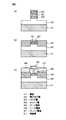
つぎに、図7、図8により図6に示した電界効果型トランジスタの製造方法、すなわち本発明に係る他の電界効果型トランジスタの製造方法を説明する。まず、図7(a)、(b)に示すように、サファイアからなる基板41上にノンドープGaNからなる電子走行層42を層厚2μm程度成長形成し、つぎにIn組成0.17程度のノンドープInAlNからなるバリア層43を層厚30nm程度成長形成する。この電子走行層42、バリア層43の成長形成工程には、例えば有機金属化学気相成長法を用いる。 Next, a method of manufacturing the field effect transistor shown in FIG. 6 with reference to FIGS. 7 and 8, that is, a method of manufacturing another field effect transistor according to the present invention will be described. First, as shown in FIGS. 7A and 7B, an
上記成長形成工程終了後、図7(c)に示すように、得られたエピ基板上に、GaN、InAlN、InGaN、InNよりも大きいエネルギー禁制帯幅を有する絶縁膜(AlNを含む)51、例えばSiO2を10nm程度堆積する。絶縁膜51の堆積には例えば光CVD装置やスパッタ装置を用いる。具体的には、ECRプラズマを用いたスパッタ装置を用いてSiO2を堆積する。つぎに、絶縁膜51を堆積した後、フォトレジスト52を塗布する。つぎに、図8(a)に示すように、通常のフォトリソグラフ技術を用いてゲート電極45を形成する領域を残してフォトレジスト52を除去して、絶縁膜51を露出させ、ついで露出した絶縁膜51をエッチング工程により除去する。すなわち、絶縁膜51のソース電極46およびドレイン電極47を形成する領域を除去する。このエッチング工程には、例えば塩素系ガスを用いたドライエッチング技術あるいはフッ酸系エッチング溶液によるウェットエッチング技術を用いる。具体的には、Cl2+CH2Cl2混合ガスを用いたICP−RIE装置を用いる。このエッチング条件は、プラズマ出力100W、試料バイアス50V、Cl2/CH2Cl2比0.3、エッチング速度0.1nm/secとする。また、このドライエッチング条件では、絶縁膜51のみならず、バリア層43、電子走行層42もエッチングできる。そこで、絶縁膜51を除去したあとそのままエッチング工程を継続し、電子走行層42の部分までエッチングする。エッチング深さはトータルで50nm程度とするが、このエッチング深さは電子走行層42の一部まで達していれば十分であるため、バリア層43の厚さ以上の深さであればよい。After the growth formation step, as shown in FIG. 7C, an insulating film (including AlN) 51 having an energy forbidden band width larger than that of GaN, InAlN, InGaN, and InN on the obtained epitaxial substrate, For example, about 10 nm of SiO2 is deposited. For the deposition of the insulating
上記エッチング工程終了後、図8(b)に示すように、フォトレジスト52を除去し、ついで再度MOCVD装置に装填してIn組成0.1程度のn型InGaNからなるキャップ層44を50nm程度成長形成する。この際、n型の導電性を持たせるために、SiH4を同時に供給することでSiをドーピングする。また、ゲート電極45の形成領域に残っている絶縁膜51がマスクとなって、電子走行層42が露出した領域にのみ選択的にSiドープのInGaNからなるキャップ層44が成長形成される。After completion of the etching process, as shown in FIG. 8B, the
キャップ層44の選択成長形成工程終了後、図8(c)に示すように、再度エッチング工程によりゲート電極45の形成領域に残っている絶縁膜51を除去し、ついで通常工程にてバリア層43上にゲート電極45を形成し、キャップ層44上にソース電極46およびドレイン電極47を形成する。 After the selective growth formation process of the
なお、図7、図8により説明した電界効果型トランジスタの製造方法においては、キャップ層44を選択的に成長形成する工程後に、ゲート電極45を形成する領域に残っている絶縁膜51をエッチング工程により除去しているが、このエッチング工程を省くことにより、バリア層43とゲート電極45との間に絶縁膜51が形成された電界効果型トランジスタを製作することができ、この場合にはゲート電極45の領域を絶縁膜51で保護することができ、ゲートリーク電流を確実に低減することができる。 7 and 8, after the step of selectively growing and forming the
また、上述実施の形態においては、窒化物半導体層の成長形成工程にMOCVD法を用いているが、他の成長法(例えば、分子線エピタキシ)法やハイドライド気相成長法およびこれらから派生した類似の成長法であってもよい。また、上述実施の形態においては、サファイアからなる基板11、41上に電子走行層12、42、バリア層13、43を形成したが、基板として他の半導体基板(例えば、SiC基板やSi基板)や絶縁体基板(例えば、ZnOなどの酸化物基板)を用いてもよい。また、上述実施の形態においては、各層の層厚を記したが、これは上述実施の形態を説明する際の具体例の一つとしてあげたものであり、他の膜厚であってもよい。 In the above-described embodiment, the MOCVD method is used in the growth formation process of the nitride semiconductor layer. However, other growth methods (for example, molecular beam epitaxy), hydride vapor phase growth methods, and similar derivatives derived therefrom are used. This growth method may be used. In the above-described embodiment, the electron transit layers 12 and 42 and the barrier layers 13 and 43 are formed on the
11…基板
12…電子走行層
13…バリア層
14…キャップ層
15…ゲート電極
16…ソース電極
17…ドレイン電極
31…絶縁膜
41…基板
42…電子走行層
43…バリア層
44…キャップ層
45…ゲート電極
46…ソース電極
47…ドレイン電極
51…絶縁膜DESCRIPTION OF
Claims (11)
Translated fromJapanesePriority Applications (1)
| Application Number | Priority Date | Filing Date | Title |
|---|---|---|---|
| JP2005357240AJP2007165431A (en) | 2005-12-12 | 2005-12-12 | Field effect transistor and manufacturing method thereof |
Applications Claiming Priority (1)
| Application Number | Priority Date | Filing Date | Title |
|---|---|---|---|
| JP2005357240AJP2007165431A (en) | 2005-12-12 | 2005-12-12 | Field effect transistor and manufacturing method thereof |
Publications (1)
| Publication Number | Publication Date |
|---|---|
| JP2007165431Atrue JP2007165431A (en) | 2007-06-28 |
Family
ID=38248035
Family Applications (1)
| Application Number | Title | Priority Date | Filing Date |
|---|---|---|---|
| JP2005357240APendingJP2007165431A (en) | 2005-12-12 | 2005-12-12 | Field effect transistor and manufacturing method thereof |
Country Status (1)
| Country | Link |
|---|---|
| JP (1) | JP2007165431A (en) |
Cited By (30)
| Publication number | Priority date | Publication date | Assignee | Title |
|---|---|---|---|---|
| JP2009099691A (en)* | 2007-10-15 | 2009-05-07 | Sanken Electric Co Ltd | Method of manufacturing field-effect semiconductor device |
| WO2009066434A1 (en)* | 2007-11-19 | 2009-05-28 | Nec Corporation | Field effect transistor and method for manufacturing the same |
| JP2009267379A (en)* | 2008-03-31 | 2009-11-12 | Ngk Insulators Ltd | Method for manufacturing epitaxial substrate and vapor deposition equipment |
| US20120315742A1 (en)* | 2011-06-08 | 2012-12-13 | Sumitomo Electric Industries, Ltd. | Method for forming nitride semiconductor device |
| JP2012256705A (en)* | 2011-06-08 | 2012-12-27 | Sumitomo Electric Ind Ltd | Manufacturing method of semiconductor device |
| JP2012256704A (en)* | 2011-06-08 | 2012-12-27 | Sumitomo Electric Ind Ltd | Semiconductor device and manufacturing method thereof |
| JP2013026410A (en)* | 2011-07-20 | 2013-02-04 | Sumitomo Electric Ind Ltd | Manufacturing method of semiconductor device |
| JP2013125918A (en)* | 2011-12-16 | 2013-06-24 | Sumitomo Electric Ind Ltd | Semiconductor device |
| CN103617950A (en)* | 2013-12-04 | 2014-03-05 | 中国电子科技集团公司第十三研究所 | Method for implementing InA1N device low-temperature ohmic contact on InGaN cap layer |
| JP2014053639A (en)* | 2008-03-24 | 2014-03-20 | Ngk Insulators Ltd | Manufacturing method of epitaxial substrate for semiconductor element |
| WO2014097526A1 (en)* | 2012-12-20 | 2014-06-26 | パナソニック株式会社 | Field effect transistor and method for producing same |
| JP2014197644A (en)* | 2013-03-29 | 2014-10-16 | トランスフォーム・ジャパン株式会社 | Compound semiconductor device and method of manufacturing the same |
| US8872226B2 (en) | 2008-03-24 | 2014-10-28 | Ngk Insulators, Ltd. | Group III nitride epitaxial substrate for semiconductor device, semiconductor device, and process for producing group III nitride epitaxial substrate for semiconductor device |
| JP2017059671A (en)* | 2015-09-16 | 2017-03-23 | 住友電気工業株式会社 | High electron mobility transistor and method of manufacturing high electron mobility transistor |
| JP2017069565A (en)* | 2015-09-30 | 2017-04-06 | 住友電気工業株式会社 | High electron mobility transistor, and manufacturing method of high electron mobility transistor |
| KR20170041692A (en)* | 2014-08-13 | 2017-04-17 | 인텔 코포레이션 | Self-aligned gate last iii-n transistors |
| JPWO2016051935A1 (en)* | 2014-10-03 | 2017-04-27 | 日本碍子株式会社 | Epitaxial substrate for semiconductor device and method of manufacturing the same |
| JP2017152467A (en)* | 2016-02-23 | 2017-08-31 | 日本電信電話株式会社 | Field effect transistor and manufacturing method thereof |
| JP2017539073A (en)* | 2014-10-30 | 2017-12-28 | インテル・コーポレーション | Source / drain regrowth for low contact resistance to 2D electron gas in gallium nitride transistors |
| US10388777B2 (en) | 2015-06-26 | 2019-08-20 | Intel Corporation | Heteroepitaxial structures with high temperature stable substrate interface material |
| US10573647B2 (en) | 2014-11-18 | 2020-02-25 | Intel Corporation | CMOS circuits using n-channel and p-channel gallium nitride transistors |
| US10658471B2 (en) | 2015-12-24 | 2020-05-19 | Intel Corporation | Transition metal dichalcogenides (TMDCS) over III-nitride heteroepitaxial layers |
| US10665708B2 (en) | 2015-05-19 | 2020-05-26 | Intel Corporation | Semiconductor devices with raised doped crystalline structures |
| US10756183B2 (en) | 2014-12-18 | 2020-08-25 | Intel Corporation | N-channel gallium nitride transistors |
| JPWO2019106843A1 (en)* | 2017-12-01 | 2020-10-08 | 三菱電機株式会社 | Manufacturing method of semiconductor devices, semiconductor devices |
| US10930500B2 (en) | 2014-09-18 | 2021-02-23 | Intel Corporation | Wurtzite heteroepitaxial structures with inclined sidewall facets for defect propagation control in silicon CMOS-compatible semiconductor devices |
| JP2021118198A (en)* | 2020-01-22 | 2021-08-10 | 富士通株式会社 | Semiconductor device |
| US11177376B2 (en) | 2014-09-25 | 2021-11-16 | Intel Corporation | III-N epitaxial device structures on free standing silicon mesas |
| US11233053B2 (en) | 2017-09-29 | 2022-01-25 | Intel Corporation | Group III-nitride (III-N) devices with reduced contact resistance and their methods of fabrication |
| US12125888B2 (en) | 2017-09-29 | 2024-10-22 | Intel Corporation | Group III-nitride (III-N) devices with reduced contact resistance and their methods of fabrication |
- 2005
- 2005-12-12JPJP2005357240Apatent/JP2007165431A/enactivePending
Cited By (44)
| Publication number | Priority date | Publication date | Assignee | Title |
|---|---|---|---|---|
| JP2009099691A (en)* | 2007-10-15 | 2009-05-07 | Sanken Electric Co Ltd | Method of manufacturing field-effect semiconductor device |
| US8680580B2 (en) | 2007-11-19 | 2014-03-25 | Renesas Electronics Corporation | Field effect transistor and process for manufacturing same |
| WO2009066434A1 (en)* | 2007-11-19 | 2009-05-28 | Nec Corporation | Field effect transistor and method for manufacturing the same |
| JP5906004B2 (en)* | 2007-11-19 | 2016-04-20 | ルネサスエレクトロニクス株式会社 | Field effect transistor and manufacturing method thereof |
| US8872226B2 (en) | 2008-03-24 | 2014-10-28 | Ngk Insulators, Ltd. | Group III nitride epitaxial substrate for semiconductor device, semiconductor device, and process for producing group III nitride epitaxial substrate for semiconductor device |
| JP2014053639A (en)* | 2008-03-24 | 2014-03-20 | Ngk Insulators Ltd | Manufacturing method of epitaxial substrate for semiconductor element |
| US8890208B2 (en) | 2008-03-24 | 2014-11-18 | Ngk Insulators, Ltd. | Group III nitride epitaxial substrate for semiconductor device, semiconductor device, and process for producing group III nitride epitaxial substrate for semiconductor device |
| JP2009267379A (en)* | 2008-03-31 | 2009-11-12 | Ngk Insulators Ltd | Method for manufacturing epitaxial substrate and vapor deposition equipment |
| JP2014123767A (en)* | 2008-03-31 | 2014-07-03 | Ngk Insulators Ltd | Epitaxial substrate for semiconductor device, and method for manufacturing epitaxial substrate for semiconductor device |
| JP2013129597A (en)* | 2008-03-31 | 2013-07-04 | Ngk Insulators Ltd | Method for manufacturing epitaxial substrate |
| JP2012256704A (en)* | 2011-06-08 | 2012-12-27 | Sumitomo Electric Ind Ltd | Semiconductor device and manufacturing method thereof |
| JP2012256705A (en)* | 2011-06-08 | 2012-12-27 | Sumitomo Electric Ind Ltd | Manufacturing method of semiconductor device |
| US20120315742A1 (en)* | 2011-06-08 | 2012-12-13 | Sumitomo Electric Industries, Ltd. | Method for forming nitride semiconductor device |
| US20160111274A1 (en)* | 2011-06-08 | 2016-04-21 | Sumitomo Electric Industries, Ltd. | Method for forming nitride semiconductor device |
| JP2013026410A (en)* | 2011-07-20 | 2013-02-04 | Sumitomo Electric Ind Ltd | Manufacturing method of semiconductor device |
| JP2013125918A (en)* | 2011-12-16 | 2013-06-24 | Sumitomo Electric Ind Ltd | Semiconductor device |
| WO2014097526A1 (en)* | 2012-12-20 | 2014-06-26 | パナソニック株式会社 | Field effect transistor and method for producing same |
| JPWO2014097526A1 (en)* | 2012-12-20 | 2017-01-12 | パナソニックIpマネジメント株式会社 | Field effect transistor and manufacturing method thereof |
| US10128363B2 (en) | 2012-12-20 | 2018-11-13 | Panasonic Intellectual Property Management Co., Ltd. | Field effect transistor |
| JP2014197644A (en)* | 2013-03-29 | 2014-10-16 | トランスフォーム・ジャパン株式会社 | Compound semiconductor device and method of manufacturing the same |
| CN103617950A (en)* | 2013-12-04 | 2014-03-05 | 中国电子科技集团公司第十三研究所 | Method for implementing InA1N device low-temperature ohmic contact on InGaN cap layer |
| KR20170041692A (en)* | 2014-08-13 | 2017-04-17 | 인텔 코포레이션 | Self-aligned gate last iii-n transistors |
| CN107078157A (en)* | 2014-08-13 | 2017-08-18 | 英特尔公司 | Self-aligned gate-last III‑N transistors |
| JP2017527988A (en)* | 2014-08-13 | 2017-09-21 | インテル・コーポレーション | Self-aligned gate last III-N transistor |
| KR102257570B1 (en)* | 2014-08-13 | 2021-05-31 | 인텔 코포레이션 | Self-aligned gate last iii-n transistors |
| US10930500B2 (en) | 2014-09-18 | 2021-02-23 | Intel Corporation | Wurtzite heteroepitaxial structures with inclined sidewall facets for defect propagation control in silicon CMOS-compatible semiconductor devices |
| US11177376B2 (en) | 2014-09-25 | 2021-11-16 | Intel Corporation | III-N epitaxial device structures on free standing silicon mesas |
| US10332975B2 (en) | 2014-10-03 | 2019-06-25 | Ngk Insulators, Ltd. | Epitaxial substrate for semiconductor device and method for manufacturing same |
| JPWO2016051935A1 (en)* | 2014-10-03 | 2017-04-27 | 日本碍子株式会社 | Epitaxial substrate for semiconductor device and method of manufacturing the same |
| JP2017539073A (en)* | 2014-10-30 | 2017-12-28 | インテル・コーポレーション | Source / drain regrowth for low contact resistance to 2D electron gas in gallium nitride transistors |
| US10573647B2 (en) | 2014-11-18 | 2020-02-25 | Intel Corporation | CMOS circuits using n-channel and p-channel gallium nitride transistors |
| US10756183B2 (en) | 2014-12-18 | 2020-08-25 | Intel Corporation | N-channel gallium nitride transistors |
| US10665708B2 (en) | 2015-05-19 | 2020-05-26 | Intel Corporation | Semiconductor devices with raised doped crystalline structures |
| US10388777B2 (en) | 2015-06-26 | 2019-08-20 | Intel Corporation | Heteroepitaxial structures with high temperature stable substrate interface material |
| JP2017059671A (en)* | 2015-09-16 | 2017-03-23 | 住友電気工業株式会社 | High electron mobility transistor and method of manufacturing high electron mobility transistor |
| JP2017069565A (en)* | 2015-09-30 | 2017-04-06 | 住友電気工業株式会社 | High electron mobility transistor, and manufacturing method of high electron mobility transistor |
| US10658471B2 (en) | 2015-12-24 | 2020-05-19 | Intel Corporation | Transition metal dichalcogenides (TMDCS) over III-nitride heteroepitaxial layers |
| JP2017152467A (en)* | 2016-02-23 | 2017-08-31 | 日本電信電話株式会社 | Field effect transistor and manufacturing method thereof |
| US11233053B2 (en) | 2017-09-29 | 2022-01-25 | Intel Corporation | Group III-nitride (III-N) devices with reduced contact resistance and their methods of fabrication |
| US11728346B2 (en) | 2017-09-29 | 2023-08-15 | Intel Corporation | Group III-nitride (III-N) devices with reduced contact resistance and their methods of fabrication |
| US12125888B2 (en) | 2017-09-29 | 2024-10-22 | Intel Corporation | Group III-nitride (III-N) devices with reduced contact resistance and their methods of fabrication |
| JPWO2019106843A1 (en)* | 2017-12-01 | 2020-10-08 | 三菱電機株式会社 | Manufacturing method of semiconductor devices, semiconductor devices |
| JP2021118198A (en)* | 2020-01-22 | 2021-08-10 | 富士通株式会社 | Semiconductor device |
| JP7543650B2 (en) | 2020-01-22 | 2024-09-03 | 富士通株式会社 | Semiconductor Device |
Similar Documents
| Publication | Publication Date | Title |
|---|---|---|
| US11699748B2 (en) | Normally-off HEMT transistor with selective generation of 2DEG channel, and manufacturing method thereof | |
| JP2007165431A (en) | Field effect transistor and manufacturing method thereof | |
| US10020361B2 (en) | Circuit structure having islands between source and drain and circuit formed | |
| US8569800B2 (en) | Field effect transistor | |
| US7709859B2 (en) | Cap layers including aluminum nitride for nitride-based transistors | |
| US9147743B2 (en) | High electron mobility transistor structure with improved breakdown voltage performance | |
| US7456443B2 (en) | Transistors having buried n-type and p-type regions beneath the source region | |
| JP5810293B2 (en) | Nitride semiconductor device | |
| JP5323527B2 (en) | Manufacturing method of GaN-based field effect transistor | |
| JP7013710B2 (en) | Manufacturing method of nitride semiconductor transistor | |
| CN101211969A (en) | High-speed and high-power nitride semiconductor device and manufacturing method thereof | |
| US20100301393A1 (en) | Field effect transistor and manufacturing method therefor | |
| JP2011238931A (en) | Enhancement mode field effect device and method of manufacturing the same | |
| US20100148184A1 (en) | Gan-based field effect transistor | |
| US12154864B2 (en) | III-nitride-based semiconductor devices on patterned substrates and method of making the same | |
| TW202145579A (en) | Depletion mode high electron mobility field effect transistor (hemt) semiconductor device having beryllium doped schottky contact layers | |
| JP4474292B2 (en) | Semiconductor device | |
| US20240030329A1 (en) | Semiconductor device and method for manufacturing the same | |
| JP4748501B2 (en) | High electron mobility transistor | |
| CN106910770B (en) | Gallium nitride-based phase inverter chip and forming method thereof | |
| CN117199124A (en) | Epitaxial structure of power device, preparation method of epitaxial structure and power device | |
| JP2009246307A (en) | Semiconductor device and method of manufacturing the same | |
| KR20220083619A (en) | High electron mobility transistor and fabricating method thereof | |
| US12432996B2 (en) | Power semiconductor device and manufacturing method thereof | |
| CN113826212B (en) | Preparation method of semiconductor structure |