JP2007157844A - Semiconductor device and manufacturing method of semiconductor device - Google Patents
Semiconductor device and manufacturing method of semiconductor deviceDownload PDFInfo
- Publication number
- JP2007157844A JP2007157844AJP2005348216AJP2005348216AJP2007157844AJP 2007157844 AJP2007157844 AJP 2007157844AJP 2005348216 AJP2005348216 AJP 2005348216AJP 2005348216 AJP2005348216 AJP 2005348216AJP 2007157844 AJP2007157844 AJP 2007157844A
- Authority
- JP
- Japan
- Prior art keywords
- semiconductor device
- electrode terminal
- hole
- semiconductor wafer
- semiconductor
- Prior art date
- Legal status (The legal status is an assumption and is not a legal conclusion. Google has not performed a legal analysis and makes no representation as to the accuracy of the status listed.)
- Pending
Links
Images


Classifications
- H—ELECTRICITY
- H01—ELECTRIC ELEMENTS
- H01L—SEMICONDUCTOR DEVICES NOT COVERED BY CLASS H10
- H01L2224/00—Indexing scheme for arrangements for connecting or disconnecting semiconductor or solid-state bodies and methods related thereto as covered by H01L24/00
- H01L2224/01—Means for bonding being attached to, or being formed on, the surface to be connected, e.g. chip-to-package, die-attach, "first-level" interconnects; Manufacturing methods related thereto
- H01L2224/42—Wire connectors; Manufacturing methods related thereto
- H01L2224/47—Structure, shape, material or disposition of the wire connectors after the connecting process
- H01L2224/48—Structure, shape, material or disposition of the wire connectors after the connecting process of an individual wire connector
- H01L2224/484—Connecting portions
- H01L2224/48463—Connecting portions the connecting portion on the bonding area of the semiconductor or solid-state body being a ball bond
Landscapes
- Internal Circuitry In Semiconductor Integrated Circuit Devices (AREA)
- Semiconductor Integrated Circuits (AREA)
Abstract
Translated fromJapaneseDescription
Translated fromJapanese本発明は、半導体装置、および斯かる半導体装置の製造方法に関し、特に、半導体装置の配線・電極形成工程後に斯かる半導体装置を組み立てる組立工程における電極端子の形成・接続方法に関する。 The present invention relates to a semiconductor device and a method for manufacturing such a semiconductor device, and more particularly, to a method for forming and connecting electrode terminals in an assembly process for assembling such a semiconductor device after a wiring / electrode forming process for the semiconductor device.
従来からの半導体製造工程では、完成した半導体ウエハから個々のチップを切り出した後に外部要因によるこれらチップ損傷からの保護、水分混入等による腐食防止を目的とした上で取り扱いを考慮した電気的な接続端子を形成するために、各種のパッケージ形状による半導体組立工程を実施している。 In the conventional semiconductor manufacturing process, after cutting individual chips from a completed semiconductor wafer, electrical connections are taken into account in order to protect these chips from damage caused by external factors and to prevent corrosion due to moisture contamination. In order to form terminals, semiconductor assembly processes using various package shapes are performed.
また、薄層、分割化された斯かるチップに対しての半導体組立工程においても、その方法はさまざまであり、とりわけ電極端子形成方法では、ワイヤボンディング、フリップチップボンディングと大きく二つの方法がある。 Also, there are various methods in the semiconductor assembling process for such thin-layered and divided chips, and there are mainly two methods in the electrode terminal forming method: wire bonding and flip chip bonding.
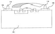
ワイヤボンディングによる電極端子形成方法では、図8に示すように、チップの電極取出端子106とリードフレーム(図示せず)のリード間に直径数十μm程度の細いAuまたはAl線118を使用して接続する方法であり、フリップチップボンディングによる電極端子形成方法では、図9に示すように、チップの電極端子106にバンプ119と呼ばれる柱状電極を形成してから、矢印で示す半導体装置の実装方向に移動させて一括して実装用基板(図示せず)と斯かるバンプ119を直接的に接続する方法であり、半導体電極部とこれを実装する基板とを最短距離で実装接続を行うことができる方法である。 In the electrode terminal forming method by wire bonding, as shown in FIG. 8, a thin Au or
しかしながら、従来のワイヤボンディングによる電極端子形成方法では、各ワイヤボンディング用電極端子とリードフレーム側での対応する端子間でそれぞれ個別にワイヤボンディングを行うために、高機能、多機能化によるLSIの高集積化に伴って、電極端子の多数化が進むため、一つのチップに対するワイヤボンディングの本数が増加してしまう。このため、ワイヤボンディング用電極端子の寸法およびワイヤボンディング用電極端子の数、ワイヤボンディング用電極端子とワイヤボンディング用電極端子同士の間隔が考慮される結果、これら要因が半導体チップの外周寸法を決定してしまうことより、LSIの高集積化に伴い、これらを実装する半導体装置のサイズの小型化が困難になる。 However, in the conventional electrode terminal forming method by wire bonding, since wire bonding is individually performed between each wire bonding electrode terminal and the corresponding terminal on the lead frame side, the high performance and multi-functionalization of the LSI can be improved. As integration increases, the number of electrode terminals increases, and the number of wire bondings for one chip increases. For this reason, the dimensions of the wire bonding electrode terminals, the number of wire bonding electrode terminals, and the distance between the wire bonding electrode terminals and the wire bonding electrode terminals are taken into consideration. As a result, it is difficult to reduce the size of a semiconductor device on which these LSIs are mounted as LSIs are highly integrated.
また、フリップチップボンディングによる電極端子形成方法では、接続対象物との熱膨張などによる接続部の応力的問題を解消するために、特殊材料を使用したバンプや接着材の開発が不可欠となることと、フリップチップボンディングによる実装後のバンプやパッドの状態の接続部分を確認することが困難となることが課題となっている。 Also, in the method of forming electrode terminals by flip-chip bonding, it is essential to develop bumps and adhesives using special materials in order to eliminate stress problems at the connection due to thermal expansion with the connection object. The problem is that it becomes difficult to confirm the connection portions of bumps and pads after mounting by flip chip bonding.
上記の課題を解決する従来技術として、半導体装置の電極端子の形成をするに際し、配線層間のコンタクトを簡便な工程で歩留まり良く良好に形成する方法として、特許文献1には、半導体基板上に第1の配線構体を構成し、この第1の配線構体上に絶縁層を介して第2の配線構体を構成し、第1の配線構体と第2の配線構体とを接続する第3の配線構体が凹部を有する金属と、斯かる凹部に埋め込まれた絶縁物とから構成されることを特徴とする配線構体が開示されている。これによって、配線の多層化、配線容量の低減、配線間干渉の低減を図り、高性能かつ小形な通信用混成IC等の半導体アナログ集積回路及びデジタル集積回路等を提供することができる。
しかしながら、上述の配線構体を備える半導体装置は、層間絶縁膜の厚さが大きくなっても配線層間のコンタクトを簡便な工程で歩留まり良く良好に形成することによって、高性能かつ小型な半導体アナログ集積回路等を提供できるものの、半導体装置が高性能かつ小型化するに伴って、斯かる半導体装置の動作時の発熱が小型化した半導体装置にかかる負荷が大きくなる。斯かる熱が半導体装置に滞留することによって、半導体装置がヒートアップして、上記回路の機能が低下することが問題となる。 However, a semiconductor device provided with the above-described wiring structure has a high-performance and small-sized semiconductor analog integrated circuit by forming a contact between wiring layers in a simple process with good yield even when the thickness of the interlayer insulating film is increased. However, as the performance of the semiconductor device is reduced and the size of the semiconductor device is increased, the load applied to the semiconductor device in which the heat generated during operation of the semiconductor device is reduced is increased. When such heat stays in the semiconductor device, the semiconductor device heats up and the function of the circuit is deteriorated.
本発明は、従来の半導体装置が有する上記問題点に鑑みてなされたものであり、本発明の目的は、半導体装置の小型化を実現すると同時に、半導体装置の動作時の発熱を廃棄することの可能な、新規かつ改良された半導体装置および斯かる半導体装置の製造方法を提供することである。 The present invention has been made in view of the above-mentioned problems of conventional semiconductor devices, and an object of the present invention is to realize miniaturization of the semiconductor device and at the same time to discard the heat generated during operation of the semiconductor device. It is possible to provide a new and improved semiconductor device and a method for manufacturing such a semiconductor device.
上記課題を解決するために、本発明のある観点によれば、接地面に設けられ、半導体ウエハ上に配線および電極端子パターンが形成されている半導体装置において、かかる電極端子パターンのうち、接地面と接続する電極端子パターンが形成されている部位には、かかる部位に設けられた電極端子パターンを貫通するようにして半導体ウエハに導通孔が形成され、半導体ウエハには、この半導体ウエハの配線および電極端子パターンが形成されている面と反対側の面から導通孔の底部に達するまで、径が導通孔の各底部を包含可能な大きさである孔部が形成され、かかる孔部には各底部および接地面を電気的に接続する一の導電体が設けられていることを特徴とする、半導体装置が提供される。 In order to solve the above problems, according to an aspect of the present invention, in a semiconductor device provided on a ground plane and having wiring and electrode terminal patterns formed on a semiconductor wafer, the ground plane of the electrode terminal patterns is provided. A conductive hole is formed in the semiconductor wafer so as to penetrate the electrode terminal pattern provided in the part at a part where the electrode terminal pattern to be connected to the semiconductor terminal is formed. A hole having a diameter that can include each bottom of the conduction hole is formed from the surface opposite to the surface on which the electrode terminal pattern is formed to reach the bottom of the conduction hole. A semiconductor device is provided, wherein one conductor for electrically connecting the bottom and the ground plane is provided.
このとき、一の導電体は、成膜加工により形成されている導電性のめっきであることとしてもよい。 At this time, the one conductor may be conductive plating formed by film formation.
このような構成とすることにより、接地面に対応する電極端子と半導体装置の裏面側から接地面に有するリードフレームへ一の導電体を介して直接的に接続することが可能となるので、半導体装置組立工程でのワイヤボンディングにおけるワイヤーの本数およびワイヤボンディング用電極端子数が低減できる。このため、電極端子の外周寸法が縮小可能となるので、半導体装置の小型化に伴う高密度化・高性能化が実現される。 By adopting such a configuration, it becomes possible to directly connect the electrode terminal corresponding to the ground plane and the lead frame on the ground plane from the back side of the semiconductor device via one conductor. It is possible to reduce the number of wires and the number of electrode terminals for wire bonding in wire bonding in the apparatus assembly process. For this reason, since the outer periphery dimension of an electrode terminal can be reduced, the high density and high performance accompanying the miniaturization of a semiconductor device are implement | achieved.
また、半導体装置の接地面と対応させる電極端子は、接地面と接する半導体装置の裏面側に設けた金属系のほうが半導体ウエハを構成する半導体材料に比べて熱伝導率が高い金属製の一の導電体からなる大口径な電極端子を介して接地される。このように、ウエハの表面側に設けられた電極等より表面積の大きい大口径な電極端子をウエハの裏面側から設けるので、半導体装置の動作時に接地面に接続される電極端子が発熱する場合でも、斯かる熱が接地面との接続媒体となる半導体装置の裏面側に設けた大口径な電極端子により多くの熱エネルギーが吸収されることによって分散される。このため、半導体装置動作中に発生する熱エネルギーが大口径な裏面側電極端子を通じてリードフレーム等の実装用基板側に伝わり半導体装置そのものに熱がこもりにくくなる。すなわち、半導体装置の動作時の廃熱効果を高めることができ、半導体装置のヒートアップにより、かかる半導体装置を備えた半導体アナログ集積回路等の機能の低下を防ぐことができる。 In addition, the electrode terminal corresponding to the ground plane of the semiconductor device is made of a metal having a higher thermal conductivity than the semiconductor material constituting the semiconductor wafer in the metal system provided on the back side of the semiconductor device in contact with the ground plane. It is grounded through a large-diameter electrode terminal made of a conductor. As described above, since a large-diameter electrode terminal having a larger surface area than the electrode provided on the front surface side of the wafer is provided from the back surface side of the wafer, even when the electrode terminal connected to the ground plane generates heat during operation of the semiconductor device. Such heat is dispersed by absorbing a large amount of heat energy by the large-diameter electrode terminal provided on the back surface side of the semiconductor device serving as a connection medium with the ground plane. For this reason, the heat energy generated during the operation of the semiconductor device is transmitted to the mounting substrate side such as the lead frame through the large-diameter back surface side electrode terminal, so that it is difficult for the semiconductor device itself to accumulate heat. That is, the waste heat effect during the operation of the semiconductor device can be enhanced, and the deterioration of the functions of the semiconductor analog integrated circuit and the like provided with the semiconductor device can be prevented by the heat-up of the semiconductor device.
上記課題を解決するために、本発明の別の観点によれば、接地面に設けられた半導体装置の半導体ウエハ上に配線および電極端子パターンを形成する工程後に、半導体装置を組み立てる工程を含む半導体装置の製造方法において、電極端子パターンが形成される面のうち、接地面と接続する電極端子パターン以外の部分を一のレジストで被膜する工程と、一のレジストで被膜されていない電極端子パターンを貫通するようにして半導体ウエハに導通孔を形成する工程と、電極端子パターンが形成される面の反対側の面に導通孔の各底部を包含可能な大きさの孔部を形成する部位以外に他のレジストを被膜する工程と、半導体ウエハの他のレジストで被膜されていない部位を半導体ウエハの反対側の面から導通孔の底部に届くまでエッチング処理をする工程と、かかるエッチング処理により形成された孔部に導通孔の各底部および接地面を導通可能にするための一の導電体を設ける工程と、これら一のおよび他のレジストを除去して、形成された半導体装置の薄層化を行う工程と、を含むことを特徴とする、半導体装置の製造方法が提供される。 In order to solve the above problems, according to another aspect of the present invention, a semiconductor including a step of assembling a semiconductor device after a step of forming wiring and electrode terminal patterns on a semiconductor wafer of the semiconductor device provided on the ground plane In the manufacturing method of the apparatus, a step of coating a portion other than the electrode terminal pattern connected to the ground surface with a single resist among surfaces on which the electrode terminal pattern is formed, and an electrode terminal pattern not coated with the one resist In addition to the step of forming a through hole in the semiconductor wafer so as to penetrate, and a portion where a hole having a size capable of including each bottom of the through hole is formed on the surface opposite to the surface on which the electrode terminal pattern is formed. Etch the process of coating another resist and the part not coated with another resist of the semiconductor wafer until it reaches the bottom of the conduction hole from the opposite surface of the semiconductor wafer. Removing the one and other resists, and a step of providing one conductor for enabling conduction between each bottom portion of the conduction hole and the ground plane in the hole formed by the etching process. And a step of thinning the formed semiconductor device. A method for manufacturing a semiconductor device is provided.
このとき、一の導電体は、導電性のめっきを所望の厚さになるまで成膜することにより形成されることとしてもよい。 At this time, the one conductor may be formed by depositing conductive plating until a desired thickness is reached.
このような構成とすることにより、半導体装置に設けられる接地面に接続する電極端子と接地面とを電気的に直接接続する導電体を設けることが容易にできるので、従来使用されていた半導体装置組立工程でのワイヤボンディングにおけるワイヤーの本数およびワイヤボンディング用電極端子数が低減され、半導体装置の小型化に伴う高密度化・高性能化が実現される。とりわけ、上記導電体を導電性のめっきを所望の厚さになるまで成膜する方法を使用することにより、かかる導電体を容易に形成できる。 By adopting such a configuration, it is possible to easily provide a conductor for electrically directly connecting the electrode terminal connected to the ground plane provided in the semiconductor device and the ground plane. The number of wires and the number of electrode terminals for wire bonding in wire bonding in the assembly process are reduced, and high density and high performance are realized along with miniaturization of semiconductor devices. In particular, such a conductor can be easily formed by using a method in which the conductor is deposited to have a desired thickness by conductive plating.
以上説明したように本発明によれば、半導体装置組立工程でのワイヤボンディングにおけるワイヤー本数を低減することができる。また、ワイヤボンディング用電極端子数の低減により、電極端子の外周寸法の縮小によって、半導体装置の寸法を縮小し、小型化することができる。さらに、半導体装置の動作時における発熱を廃棄する廃熱効果が高まる。 As described above, according to the present invention, the number of wires in wire bonding in the semiconductor device assembly process can be reduced. Further, by reducing the number of electrode terminals for wire bonding, the size of the semiconductor device can be reduced and the size can be reduced by reducing the outer peripheral dimensions of the electrode terminals. Furthermore, the waste heat effect of discarding heat generated during operation of the semiconductor device is enhanced.
以下に添付図面を参照しながら、本発明の好適な実施の形態について詳細に説明する。なお、本明細書および図面において、実質的に同一の機能構成を有する構成要素については、同一の符号を付することにより重複説明を省略する。 Exemplary embodiments of the present invention will be described below in detail with reference to the accompanying drawings. In the present specification and drawings, components having substantially the same functional configuration are denoted by the same reference numerals, and redundant description is omitted.
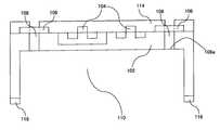
まず、本発明の半導体装置の構成について、図面を使用しながら説明する。図1は、本発明の半導体装置の一実施形態の模式的な断面図である。本実施形態の半導体装置100は、GaAsやSi等からなる半導体ウエハ102の上に、CuやAl等からなる配線パターン104および電極端子パターン106がスパッタ法や蒸着法等により形成されている。電極端子パターン106のうち、リードフレーム等の電気信号をやり取りする際の基準電位(0V)とみなされる接地面(以下、GNDと称する)と接続する電極端子パターン106が形成されている部位には、かかる部位に設けられた電極端子パターン106を貫通するようにして半導体ウエハ102に導通孔となるVIAホール108がエッチング等により形成されている。 First, the structure of the semiconductor device of the present invention will be described with reference to the drawings. FIG. 1 is a schematic cross-sectional view of an embodiment of a semiconductor device of the present invention. In the
半導体ウエハ102の配線パターン104および電極端子パターン106が形成されている面102aと反対側の面となる裏面102bには、VIAホール108の各底部108aを包含可能な大きさの径を有する孔部である大口径ホール110が設けられ、この大口径ホール110は、半導体ウエハ102の裏面102bからVIAホール108の底部108aに達するまでの深さを有する。この大口径ホール110には、VIAホール108の各底部108aおよびGNDを電気的に接続するための一の導電体として裏面側電極端子用メタル112が設けられている。この裏面側電極端子用メタル112は、本実施形態では、後述するように金(Au)等の導電性の大きい金属からなる導電性のめっきの成膜加工により形成されている。 On the
このように、GNDに対応する電極端子106と半導体装置100の裏面側からGNDとなるリードフレーム(図示せず)へ裏面側電極端子用メタル112を介して直接的に接続できるので、半導体装置組立工程でのワイヤボンディングにおけるワイヤーの本数およびワイヤボンディング用電極端子数が低減可能となる。このため、電極端子の外周寸法が縮小可能となるので、半導体装置100の小型化に伴う高密度化が実現される。 As described above, since the
また、半導体装置100のGNDと対応させる電極端子106は、GNDと接する大口径な電極端子となる裏面側電極端子用メタル112を介して接地されることにより、半導体装置100の動作時にGNDに接続される電極端子106の発熱を裏面側電極端子用メタル112で分散されるので、前述の半導体装置100の動作時の発熱の廃熱効果が高まる。このため、半導体装置100のヒートアップによって、かかる半導体装置100を備えた半導体アナログ集積回路等の機能の低下を防ぐことができる。 Further, the
さらに、GNDと接する上述の大口径な電極端子を半導体材料からなる半導体ウエハ102に比べて熱伝導率が高い金(Au)等の金属系材質で表面積を大きく形成することによって、より多くの熱エネルギーを吸収できる。このため、結果的に半導体装置100の動作中に発生する熱エネルギーが大口径な裏面側電極端子用メタル112を通じてリードフレーム等の実装用基板側に伝わり、半導体装置100そのものに熱がこもりにくくなり、かかる廃熱効果の向上が実現される。 Further, by forming the large-diameter electrode terminal in contact with GND with a metal-based material such as gold (Au) having a higher thermal conductivity than that of the
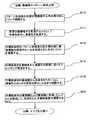
次に、本実施形態の半導体装置100の製造方法について、図面を使用しながら説明する。図2は、本実施形態の半導体装置100の製造方法を説明するためのフローチャートであり、図3〜7は、図2で示すフローチャートの工程S10〜S18までの各工程における本実施形態の半導体装置100の模式的な断面図である。 Next, a method for manufacturing the
本発明の半導体装置の製造方法は、半導体装置の配線・電極形成工程後に斯かる半導体装置を組み立てる各種のパッケージ形状による組立工程に特徴を有する。本実施形態の半導体装置100の製造方法において、図2で示す半導体装置100の組立工程では、半導体ウエハ102上に配線パターン104および電極端子パターン106を形成する工程後に、まず、電極端子パターン106が形成される面102aのうち、GNDに対応する電極端子パターン106以外の部分を図3に示すように第1のレジストとなるフォトレジスト114で被膜する(図2で示す工程S10)。 The method for manufacturing a semiconductor device according to the present invention is characterized by an assembling process using various package shapes for assembling the semiconductor device after the wiring / electrode forming process of the semiconductor device. In the manufacturing method of the
その後、図4に示すように、GNDに対応している電極端子パターン106、換言すると、フォトレジスト114で被膜されていない電極端子パターン106を貫通するようにして半導体ウエハ102にVIAホール108をエッチング処理等により形成する(図2で示す工程S12)。なお、このときのVIAホール108の深さは、100um以上の深さを確保することが製造過程において加工精度上厳しいため、100um以下を想定するものとする。 Thereafter, as shown in FIG. 4, the
半導体ウエハ102にVIAホール108を形成後、電極端子パターン106が形成される面102aの反対側の面となる裏側面102bに工程S12で形成したVIAホール108の各底部108aを包含可能な大きさの孔部である大口径ホール110を形成するために、図5で示すように、大口径ホール110を形成する部位以外に、第2のレジストとなるフォトレジスト116を被膜する(図2で示す工程S14)。 After forming the
その後、工程S14で半導体ウエハ102のフォトレジスト116で被膜されていない部位に対し、図6で示すように、半導体ウエハ102の反対側の面となる裏面102bからVIAホール108の底部となる底面108aが確認できる深さまでエッチング処理をすることにより、上記の大口径ホール110を形成する(図2で示す工程S16)。これにより、各電極端子上から形成された各電極端子用VIAホール108と大口径ホール110の接続が可能となる。なお、大口径ホール110は、製造条件の許容範囲内でなるべく大きく、かつ深く形成される程、上述した本発明の効果がより発揮されるので好ましい。 After that, as shown in FIG. 6, the
次に、形成された大口径ホール110に対し、図7で示すように、VIAホール108の各底部108aとGNDとを電気的に接続するための一の導電体として、導電性のめっきを所望の厚さになるまで成膜することによって裏面側電極端子用メタル112が形成される(図2で示す工程S18)。このときの導電性めっきの好適な材質としては、電気伝導や熱伝導に非常に優れ、かつ酸化しにくいことによる経時変化が少ない点からして、金等が好ましいが、銅等の他の金属でも代用可能である。なお、このとき形成される裏面側電極端子用メタル112の厚さは、次の工程S20での薄層化における目標基板厚よりもやや厚めになるような厚さとすることが好ましい。 Next, with respect to the formed large-
その後、オゾン溶解法等によりフォトレジスト114、116を除去してから、形成された半導体装置100を所望の厚さになるまでの薄層化を行い(図2で示す工程S20)、図1に示す装置の形態をもって半導体装置100の完成とし、かかる工程S20以降は、チップ化工程等を行うこととする。 Thereafter, the
以上説明したように、本発明の半導体装置100の製造方法は、半導体ウエハ102の裏面側102bに半導体ウエハ102の表面側102aから形成した各VIAホール108を包含可能な大きさの大口径ホール110を形成してから、半導体装置100に設けられるGNDに接続する電極端子106とGNDとを電気的に直接接続する導電体となる裏面側電極端子用メタル112を導電性めっきの成膜加工で設けることにより、ウエハ102の表面側に設けた電極端子106とGNDが導通するので、従来のように半導体装置組立工程でのワイヤボンディングにおけるワイヤーの本数やワイヤボンディング用電極端子数が低減できる。 As described above, the manufacturing method of the
また、半導体装置100のGNDと対応させる電極端子106が大口径な電極端子である裏面側電極端子用メタル112を介して接地されることによって、半導体装置100の動作時にGNDに接続される電極端子106の発熱を裏面側電極端子用メタル112で分散できる。このため、半導体装置の小型化に伴う高密度化を実現した上で前述の半導体装置100の動作時の発熱の廃熱効果を高めることができる。 Further, the
以上、添付図面を参照しながら本発明の好適な実施形態について説明したが、本発明は係る例に限定されないことは言うまでもない。当業者であれば、特許請求の範囲に記載された範疇内において、各種の変更例または修正例に想到し得ることは明らかであり、それらについても当然に本発明の技術的範囲に属するものと了解される。 As mentioned above, although preferred embodiment of this invention was described referring an accompanying drawing, it cannot be overemphasized that this invention is not limited to the example which concerns. It will be apparent to those skilled in the art that various changes and modifications can be made within the scope of the claims, and these are naturally within the technical scope of the present invention. Understood.
例えば、上述の実施形態では、半導体ウエハ102の裏面側から形成した大口径ホール110にVIAホール108の各底部108aとGNDを電気的に接続するために導電性めっきの成膜加工により形成された裏面側電極端子用メタル112が設けられているが、VIAホール108の各底部108aとGNDを電気的に接続できれば、成膜加工によって形成された裏面側電極端子用メタル112に限定されず、他の製造方法で形成された金属板等の一の導電体で代用することも可能である。 For example, in the above-described embodiment, it is formed by conductive plating film forming processing in order to electrically connect each
本発明は、半導体装置、および斯かる半導体装置の製造方法に適用可能であり、特に、ワイヤボンディング方法を用いずにリードフレームGND部への実装接地が可能な半導体装置に適用可能である。 The present invention can be applied to a semiconductor device and a method for manufacturing such a semiconductor device, and in particular, can be applied to a semiconductor device that can be mounted and grounded to a lead frame GND portion without using a wire bonding method.
100 半導体装置
102 半導体ウエハ
102a 配線および電極端子パターンが形成されている面
102b 配線および電極端子パターンが形成されている面と反対側の面(裏側面)
104 配線パターン
106 電極端子パターン
108 導通孔(VIAホール)
108a (VIAホールの)底部
110 孔部(大口径ホール)
112 一の導電体(裏面電極端子用メタル)
114 一のレジスト(フォトレジスト)
116 他のレジスト(フォトレジスト)100
104
108a (VIA hole) bottom 110 hole (large-diameter hole)
112 One conductor (metal for back electrode terminal)
114 One resist (photoresist)
116 Other resists (photoresists)
Claims (4)
Translated fromJapanese前記電極端子パターンのうち、前記接地面と接続する電極端子パターンが形成されている部位には、該部位に設けられた前記電極端子パターンを貫通するようにして前記半導体ウエハに導通孔が形成され、
前記半導体ウエハには、該半導体ウエハの前記配線および電極端子パターンが形成されている面と反対側の面から前記導通孔の底部に達するまで、径が前記導通孔の各底部を包含可能な大きさである孔部が形成され、該孔部には前記各底部および前記接地面を電気的に接続する一の導電体が設けられていることを特徴とする、半導体装置。In the semiconductor device provided on the ground plane and formed with wiring and electrode terminal patterns on the semiconductor wafer,
Of the electrode terminal pattern, a conductive hole is formed in the semiconductor wafer at a portion where the electrode terminal pattern connected to the ground plane is formed so as to penetrate the electrode terminal pattern provided in the portion. ,
The diameter of the semiconductor wafer is such that the diameter of the semiconductor wafer can include each bottom portion of the conduction hole until it reaches the bottom portion of the conduction hole from the surface opposite to the surface on which the wiring and electrode terminal patterns are formed. The semiconductor device is characterized in that a hole is formed, and the hole is provided with one conductor for electrically connecting the bottom and the ground plane.
前記電極端子パターンが形成される面のうち、前記接地面と接続する電極端子パターン以外の部分を一のレジストで被膜する工程と、
前記一のレジストで被膜されていない前記電極端子パターンを貫通するようにして前記半導体ウエハに導通孔を形成する工程と、
前記電極端子パターンが形成される面の反対側の面に前記導通孔の各底部を包含可能な大きさの孔部を形成する部位以外に他のレジストを被膜する工程と、
前記半導体ウエハの前記他のレジストで被膜されていない部位を前記反対側の面から前記導通孔の底部に届くまでエッチング処理をする工程と、
前記エッチング処理により形成された前記孔部に前記導通孔の各底部および前記接地面を導通可能にするための一の導電体を設ける工程と、
前記一のおよび他のレジストを除去して、形成された半導体装置の薄層化を行う工程と、
を含むことを特徴とする、半導体装置の製造方法。In a method of manufacturing a semiconductor device including a step of assembling the semiconductor device after the step of forming wiring and electrode terminal patterns on the semiconductor wafer of the semiconductor device provided on the ground plane,
Of the surface on which the electrode terminal pattern is formed, a step of coating a portion other than the electrode terminal pattern connected to the ground plane with a single resist,
Forming a conduction hole in the semiconductor wafer so as to penetrate the electrode terminal pattern not coated with the one resist;
Coating a resist other than a portion for forming a hole having a size capable of including each bottom of the conduction hole on the surface opposite to the surface on which the electrode terminal pattern is formed;
Etching the semiconductor wafer until the part not coated with the other resist reaches the bottom of the conduction hole from the opposite surface; and
A step of providing one conductor for enabling conduction between each bottom of the conduction hole and the ground plane in the hole formed by the etching process;
Removing the one and other resists and thinning the formed semiconductor device; and
A method for manufacturing a semiconductor device, comprising:
Priority Applications (1)
| Application Number | Priority Date | Filing Date | Title |
|---|---|---|---|
| JP2005348216AJP2007157844A (en) | 2005-12-01 | 2005-12-01 | Semiconductor device and manufacturing method of semiconductor device |
Applications Claiming Priority (1)
| Application Number | Priority Date | Filing Date | Title |
|---|---|---|---|
| JP2005348216AJP2007157844A (en) | 2005-12-01 | 2005-12-01 | Semiconductor device and manufacturing method of semiconductor device |
Publications (1)
| Publication Number | Publication Date |
|---|---|
| JP2007157844Atrue JP2007157844A (en) | 2007-06-21 |
Family
ID=38241853
Family Applications (1)
| Application Number | Title | Priority Date | Filing Date |
|---|---|---|---|
| JP2005348216APendingJP2007157844A (en) | 2005-12-01 | 2005-12-01 | Semiconductor device and manufacturing method of semiconductor device |
Country Status (1)
| Country | Link |
|---|---|
| JP (1) | JP2007157844A (en) |
Cited By (14)
| Publication number | Priority date | Publication date | Assignee | Title |
|---|---|---|---|---|
| EP2183770A4 (en)* | 2007-07-31 | 2010-08-04 | Tessera Inc | Semiconductor packaging process using through silicon vias |
| US8310036B2 (en) | 2007-03-05 | 2012-11-13 | DigitalOptics Corporation Europe Limited | Chips having rear contacts connected by through vias to front contacts |
| US8432045B2 (en) | 2010-11-15 | 2013-04-30 | Tessera, Inc. | Conductive pads defined by embedded traces |
| US8587126B2 (en) | 2010-12-02 | 2013-11-19 | Tessera, Inc. | Stacked microelectronic assembly with TSVs formed in stages with plural active chips |
| US8610264B2 (en) | 2010-12-08 | 2013-12-17 | Tessera, Inc. | Compliant interconnects in wafers |
| US8610259B2 (en) | 2010-09-17 | 2013-12-17 | Tessera, Inc. | Multi-function and shielded 3D interconnects |
| US8637968B2 (en) | 2010-12-02 | 2014-01-28 | Tessera, Inc. | Stacked microelectronic assembly having interposer connecting active chips |
| US8653644B2 (en) | 2006-11-22 | 2014-02-18 | Tessera, Inc. | Packaged semiconductor chips with array |
| US8704347B2 (en) | 2006-11-22 | 2014-04-22 | Tessera, Inc. | Packaged semiconductor chips |
| US8736066B2 (en) | 2010-12-02 | 2014-05-27 | Tessera, Inc. | Stacked microelectronic assemby with TSVS formed in stages and carrier above chip |
| US8791575B2 (en) | 2010-07-23 | 2014-07-29 | Tessera, Inc. | Microelectronic elements having metallic pads overlying vias |
| US8796135B2 (en) | 2010-07-23 | 2014-08-05 | Tessera, Inc. | Microelectronic elements with rear contacts connected with via first or via middle structures |
| US8847380B2 (en) | 2010-09-17 | 2014-09-30 | Tessera, Inc. | Staged via formation from both sides of chip |
| US9640437B2 (en) | 2010-07-23 | 2017-05-02 | Tessera, Inc. | Methods of forming semiconductor elements using micro-abrasive particle stream |
Citations (4)
| Publication number | Priority date | Publication date | Assignee | Title |
|---|---|---|---|---|
| JPH0399470A (en)* | 1989-09-12 | 1991-04-24 | Mitsubishi Electric Corp | Manufacturing method of semiconductor device |
| JPH03278539A (en)* | 1990-03-28 | 1991-12-10 | Nec Corp | Semiconductor device |
| JPH0969593A (en)* | 1995-08-31 | 1997-03-11 | Mitsubishi Electric Corp | Semiconductor device and its package |
| JP2004152810A (en)* | 2002-10-28 | 2004-05-27 | Sharp Corp | Semiconductor device and stacked semiconductor device |
- 2005
- 2005-12-01JPJP2005348216Apatent/JP2007157844A/enactivePending
Patent Citations (4)
| Publication number | Priority date | Publication date | Assignee | Title |
|---|---|---|---|---|
| JPH0399470A (en)* | 1989-09-12 | 1991-04-24 | Mitsubishi Electric Corp | Manufacturing method of semiconductor device |
| JPH03278539A (en)* | 1990-03-28 | 1991-12-10 | Nec Corp | Semiconductor device |
| JPH0969593A (en)* | 1995-08-31 | 1997-03-11 | Mitsubishi Electric Corp | Semiconductor device and its package |
| JP2004152810A (en)* | 2002-10-28 | 2004-05-27 | Sharp Corp | Semiconductor device and stacked semiconductor device |
Cited By (32)
| Publication number | Priority date | Publication date | Assignee | Title |
|---|---|---|---|---|
| US9548254B2 (en) | 2006-11-22 | 2017-01-17 | Tessera, Inc. | Packaged semiconductor chips with array |
| US8704347B2 (en) | 2006-11-22 | 2014-04-22 | Tessera, Inc. | Packaged semiconductor chips |
| US8653644B2 (en) | 2006-11-22 | 2014-02-18 | Tessera, Inc. | Packaged semiconductor chips with array |
| US9070678B2 (en) | 2006-11-22 | 2015-06-30 | Tessera, Inc. | Packaged semiconductor chips with array |
| US8405196B2 (en) | 2007-03-05 | 2013-03-26 | DigitalOptics Corporation Europe Limited | Chips having rear contacts connected by through vias to front contacts |
| US8310036B2 (en) | 2007-03-05 | 2012-11-13 | DigitalOptics Corporation Europe Limited | Chips having rear contacts connected by through vias to front contacts |
| US8735205B2 (en) | 2007-03-05 | 2014-05-27 | Invensas Corporation | Chips having rear contacts connected by through vias to front contacts |
| EP2183770A4 (en)* | 2007-07-31 | 2010-08-04 | Tessera Inc | Semiconductor packaging process using through silicon vias |
| US8193615B2 (en) | 2007-07-31 | 2012-06-05 | DigitalOptics Corporation Europe Limited | Semiconductor packaging process using through silicon vias |
| US8735287B2 (en) | 2007-07-31 | 2014-05-27 | Invensas Corp. | Semiconductor packaging process using through silicon vias |
| US9640437B2 (en) | 2010-07-23 | 2017-05-02 | Tessera, Inc. | Methods of forming semiconductor elements using micro-abrasive particle stream |
| US8791575B2 (en) | 2010-07-23 | 2014-07-29 | Tessera, Inc. | Microelectronic elements having metallic pads overlying vias |
| US8796135B2 (en) | 2010-07-23 | 2014-08-05 | Tessera, Inc. | Microelectronic elements with rear contacts connected with via first or via middle structures |
| US9355948B2 (en) | 2010-09-17 | 2016-05-31 | Tessera, Inc. | Multi-function and shielded 3D interconnects |
| US9362203B2 (en) | 2010-09-17 | 2016-06-07 | Tessera, Inc. | Staged via formation from both sides of chip |
| US10354942B2 (en) | 2010-09-17 | 2019-07-16 | Tessera, Inc. | Staged via formation from both sides of chip |
| US9847277B2 (en) | 2010-09-17 | 2017-12-19 | Tessera, Inc. | Staged via formation from both sides of chip |
| US8809190B2 (en) | 2010-09-17 | 2014-08-19 | Tessera, Inc. | Multi-function and shielded 3D interconnects |
| US8847380B2 (en) | 2010-09-17 | 2014-09-30 | Tessera, Inc. | Staged via formation from both sides of chip |
| US8610259B2 (en) | 2010-09-17 | 2013-12-17 | Tessera, Inc. | Multi-function and shielded 3D interconnects |
| US8432045B2 (en) | 2010-11-15 | 2013-04-30 | Tessera, Inc. | Conductive pads defined by embedded traces |
| US8772908B2 (en) | 2010-11-15 | 2014-07-08 | Tessera, Inc. | Conductive pads defined by embedded traces |
| US9368476B2 (en) | 2010-12-02 | 2016-06-14 | Tessera, Inc. | Stacked microelectronic assembly with TSVs formed in stages with plural active chips |
| US9269692B2 (en) | 2010-12-02 | 2016-02-23 | Tessera, Inc. | Stacked microelectronic assembly with TSVS formed in stages and carrier above chip |
| US9099296B2 (en) | 2010-12-02 | 2015-08-04 | Tessera, Inc. | Stacked microelectronic assembly with TSVS formed in stages with plural active chips |
| US8587126B2 (en) | 2010-12-02 | 2013-11-19 | Tessera, Inc. | Stacked microelectronic assembly with TSVs formed in stages with plural active chips |
| US9620437B2 (en) | 2010-12-02 | 2017-04-11 | Tessera, Inc. | Stacked microelectronic assembly with TSVS formed in stages and carrier above chip |
| US8637968B2 (en) | 2010-12-02 | 2014-01-28 | Tessera, Inc. | Stacked microelectronic assembly having interposer connecting active chips |
| US8736066B2 (en) | 2010-12-02 | 2014-05-27 | Tessera, Inc. | Stacked microelectronic assemby with TSVS formed in stages and carrier above chip |
| US8610264B2 (en) | 2010-12-08 | 2013-12-17 | Tessera, Inc. | Compliant interconnects in wafers |
| US9224649B2 (en) | 2010-12-08 | 2015-12-29 | Tessera, Inc. | Compliant interconnects in wafers |
| US8796828B2 (en) | 2010-12-08 | 2014-08-05 | Tessera, Inc. | Compliant interconnects in wafers |
Similar Documents
| Publication | Publication Date | Title |
|---|---|---|
| KR100709662B1 (en) | Semiconductor device and manufacturing method thereof | |
| JP4400802B2 (en) | Lead frame, manufacturing method thereof, and semiconductor device | |
| JP4307284B2 (en) | Manufacturing method of semiconductor device | |
| US7271466B2 (en) | Semiconductor device with sidewall wiring | |
| KR100917745B1 (en) | Semiconductor device and manufacturing method thereof | |
| JP3684978B2 (en) | SEMICONDUCTOR DEVICE, ITS MANUFACTURING METHOD, AND ELECTRONIC DEVICE | |
| JP4775007B2 (en) | Semiconductor device and manufacturing method thereof | |
| US20070269931A1 (en) | Wafer level package and method of fabricating the same | |
| JP6100480B2 (en) | Semiconductor device and manufacturing method thereof | |
| US20070035020A1 (en) | Semiconductor Apparatus and Semiconductor Module | |
| JP2008532292A (en) | Structure and method for forming flip chip devices | |
| JP2002184904A (en) | Semiconductor device manufacturing method and semiconductor device | |
| JP3651346B2 (en) | Semiconductor device and manufacturing method thereof | |
| JP2007157844A (en) | Semiconductor device and manufacturing method of semiconductor device | |
| KR20080090826A (en) | Manufacturing method of semiconductor device for multi chip stack package | |
| JP2009295676A (en) | Semiconductor device and production method thereof | |
| US20220344300A1 (en) | Electronic device and manufacturing method thereof | |
| TW202131472A (en) | Semiconductor device and method of fabricating the same | |
| CN105470144B (en) | Coreless layer packaging substrate and manufacturing method thereof | |
| EP1478021A1 (en) | Semiconductor device and manufacturing method thereof | |
| JP2007036060A (en) | Semiconductor device and manufacturing method thereof | |
| US6908845B2 (en) | Integrated circuit die and an electronic assembly having a three-dimensional interconnection scheme | |
| JP2008053430A (en) | Semiconductor device and manufacturing method thereof | |
| JP3970211B2 (en) | Semiconductor device and manufacturing method thereof | |
| JP4678720B2 (en) | Circuit board and manufacturing method thereof, semiconductor device and manufacturing method thereof |
Legal Events
| Date | Code | Title | Description |
|---|---|---|---|
| A621 | Written request for application examination | Free format text:JAPANESE INTERMEDIATE CODE: A621 Effective date:20080220 | |
| A977 | Report on retrieval | Free format text:JAPANESE INTERMEDIATE CODE: A971007 Effective date:20091217 | |
| A131 | Notification of reasons for refusal | Effective date:20100106 Free format text:JAPANESE INTERMEDIATE CODE: A131 | |
| A02 | Decision of refusal | Effective date:20100427 Free format text:JAPANESE INTERMEDIATE CODE: A02 |