JP2007157314A - Write-once optical disc and optical recording method - Google Patents
Write-once optical disc and optical recording methodDownload PDFInfo
- Publication number
- JP2007157314A JP2007157314AJP2006279961AJP2006279961AJP2007157314AJP 2007157314 AJP2007157314 AJP 2007157314AJP 2006279961 AJP2006279961 AJP 2006279961AJP 2006279961 AJP2006279961 AJP 2006279961AJP 2007157314 AJP2007157314 AJP 2007157314A
- Authority
- JP
- Japan
- Prior art keywords
- layer
- recording
- write
- optical disc
- reaction
- Prior art date
- Legal status (The legal status is an assumption and is not a legal conclusion. Google has not performed a legal analysis and makes no representation as to the accuracy of the status listed.)
- Withdrawn
Links
Images


Classifications
- G—PHYSICS
- G11—INFORMATION STORAGE
- G11B—INFORMATION STORAGE BASED ON RELATIVE MOVEMENT BETWEEN RECORD CARRIER AND TRANSDUCER
- G11B7/00—Recording or reproducing by optical means, e.g. recording using a thermal beam of optical radiation by modifying optical properties or the physical structure, reproducing using an optical beam at lower power by sensing optical properties; Record carriers therefor
- G11B7/24—Record carriers characterised by shape, structure or physical properties, or by the selection of the material
- G11B7/2403—Layers; Shape, structure or physical properties thereof
- G11B7/24067—Combinations of two or more layers with specific interrelation
- G—PHYSICS
- G11—INFORMATION STORAGE
- G11B—INFORMATION STORAGE BASED ON RELATIVE MOVEMENT BETWEEN RECORD CARRIER AND TRANSDUCER
- G11B7/00—Recording or reproducing by optical means, e.g. recording using a thermal beam of optical radiation by modifying optical properties or the physical structure, reproducing using an optical beam at lower power by sensing optical properties; Record carriers therefor
- G11B7/24—Record carriers characterised by shape, structure or physical properties, or by the selection of the material
- G11B7/241—Record carriers characterised by shape, structure or physical properties, or by the selection of the material characterised by the selection of the material
- G11B7/242—Record carriers characterised by shape, structure or physical properties, or by the selection of the material characterised by the selection of the material of recording layers
- G11B7/243—Record carriers characterised by shape, structure or physical properties, or by the selection of the material characterised by the selection of the material of recording layers comprising inorganic materials only, e.g. ablative layers
- G11B7/2433—Metals or elements of Groups 13, 14, 15 or 16 of the Periodic Table, e.g. B, Si, Ge, As, Sb, Bi, Se or Te
- G—PHYSICS
- G11—INFORMATION STORAGE
- G11B—INFORMATION STORAGE BASED ON RELATIVE MOVEMENT BETWEEN RECORD CARRIER AND TRANSDUCER
- G11B7/00—Recording or reproducing by optical means, e.g. recording using a thermal beam of optical radiation by modifying optical properties or the physical structure, reproducing using an optical beam at lower power by sensing optical properties; Record carriers therefor
- G11B7/24—Record carriers characterised by shape, structure or physical properties, or by the selection of the material
- G11B7/241—Record carriers characterised by shape, structure or physical properties, or by the selection of the material characterised by the selection of the material
- G11B7/242—Record carriers characterised by shape, structure or physical properties, or by the selection of the material characterised by the selection of the material of recording layers
- G11B7/243—Record carriers characterised by shape, structure or physical properties, or by the selection of the material characterised by the selection of the material of recording layers comprising inorganic materials only, e.g. ablative layers
- G11B7/2437—Non-metallic elements
- G—PHYSICS
- G11—INFORMATION STORAGE
- G11B—INFORMATION STORAGE BASED ON RELATIVE MOVEMENT BETWEEN RECORD CARRIER AND TRANSDUCER
- G11B7/00—Recording or reproducing by optical means, e.g. recording using a thermal beam of optical radiation by modifying optical properties or the physical structure, reproducing using an optical beam at lower power by sensing optical properties; Record carriers therefor
- G11B7/24—Record carriers characterised by shape, structure or physical properties, or by the selection of the material
- G11B7/241—Record carriers characterised by shape, structure or physical properties, or by the selection of the material characterised by the selection of the material
- G11B7/242—Record carriers characterised by shape, structure or physical properties, or by the selection of the material characterised by the selection of the material of recording layers
- G11B7/243—Record carriers characterised by shape, structure or physical properties, or by the selection of the material characterised by the selection of the material of recording layers comprising inorganic materials only, e.g. ablative layers
- G11B2007/24302—Metals or metalloids
- G11B2007/24306—Metals or metalloids transition metal elements of groups 3-10
- G—PHYSICS
- G11—INFORMATION STORAGE
- G11B—INFORMATION STORAGE BASED ON RELATIVE MOVEMENT BETWEEN RECORD CARRIER AND TRANSDUCER
- G11B7/00—Recording or reproducing by optical means, e.g. recording using a thermal beam of optical radiation by modifying optical properties or the physical structure, reproducing using an optical beam at lower power by sensing optical properties; Record carriers therefor
- G11B7/24—Record carriers characterised by shape, structure or physical properties, or by the selection of the material
- G11B7/241—Record carriers characterised by shape, structure or physical properties, or by the selection of the material characterised by the selection of the material
- G11B7/242—Record carriers characterised by shape, structure or physical properties, or by the selection of the material characterised by the selection of the material of recording layers
- G11B7/243—Record carriers characterised by shape, structure or physical properties, or by the selection of the material characterised by the selection of the material of recording layers comprising inorganic materials only, e.g. ablative layers
- G11B2007/24302—Metals or metalloids
- G11B2007/24312—Metals or metalloids group 14 elements (e.g. Si, Ge, Sn)
- G—PHYSICS
- G11—INFORMATION STORAGE
- G11B—INFORMATION STORAGE BASED ON RELATIVE MOVEMENT BETWEEN RECORD CARRIER AND TRANSDUCER
- G11B7/00—Recording or reproducing by optical means, e.g. recording using a thermal beam of optical radiation by modifying optical properties or the physical structure, reproducing using an optical beam at lower power by sensing optical properties; Record carriers therefor
- G11B7/24—Record carriers characterised by shape, structure or physical properties, or by the selection of the material
- G11B7/241—Record carriers characterised by shape, structure or physical properties, or by the selection of the material characterised by the selection of the material
- G11B7/242—Record carriers characterised by shape, structure or physical properties, or by the selection of the material characterised by the selection of the material of recording layers
- G11B7/243—Record carriers characterised by shape, structure or physical properties, or by the selection of the material characterised by the selection of the material of recording layers comprising inorganic materials only, e.g. ablative layers
- G11B2007/24318—Non-metallic elements
- G11B2007/2432—Oxygen
- G—PHYSICS
- G11—INFORMATION STORAGE
- G11B—INFORMATION STORAGE BASED ON RELATIVE MOVEMENT BETWEEN RECORD CARRIER AND TRANSDUCER
- G11B7/00—Recording or reproducing by optical means, e.g. recording using a thermal beam of optical radiation by modifying optical properties or the physical structure, reproducing using an optical beam at lower power by sensing optical properties; Record carriers therefor
- G11B7/24—Record carriers characterised by shape, structure or physical properties, or by the selection of the material
- G11B7/241—Record carriers characterised by shape, structure or physical properties, or by the selection of the material characterised by the selection of the material
- G11B7/242—Record carriers characterised by shape, structure or physical properties, or by the selection of the material characterised by the selection of the material of recording layers
- G11B7/243—Record carriers characterised by shape, structure or physical properties, or by the selection of the material characterised by the selection of the material of recording layers comprising inorganic materials only, e.g. ablative layers
- G11B2007/24318—Non-metallic elements
- G11B2007/24322—Nitrogen
- G—PHYSICS
- G11—INFORMATION STORAGE
- G11B—INFORMATION STORAGE BASED ON RELATIVE MOVEMENT BETWEEN RECORD CARRIER AND TRANSDUCER
- G11B7/00—Recording or reproducing by optical means, e.g. recording using a thermal beam of optical radiation by modifying optical properties or the physical structure, reproducing using an optical beam at lower power by sensing optical properties; Record carriers therefor
- G11B7/24—Record carriers characterised by shape, structure or physical properties, or by the selection of the material
- G11B7/241—Record carriers characterised by shape, structure or physical properties, or by the selection of the material characterised by the selection of the material
- G11B7/242—Record carriers characterised by shape, structure or physical properties, or by the selection of the material characterised by the selection of the material of recording layers
- G11B7/243—Record carriers characterised by shape, structure or physical properties, or by the selection of the material characterised by the selection of the material of recording layers comprising inorganic materials only, e.g. ablative layers
- G11B2007/24318—Non-metallic elements
- G11B2007/24328—Carbon
- G—PHYSICS
- G11—INFORMATION STORAGE
- G11B—INFORMATION STORAGE BASED ON RELATIVE MOVEMENT BETWEEN RECORD CARRIER AND TRANSDUCER
- G11B7/00—Recording or reproducing by optical means, e.g. recording using a thermal beam of optical radiation by modifying optical properties or the physical structure, reproducing using an optical beam at lower power by sensing optical properties; Record carriers therefor
- G11B7/24—Record carriers characterised by shape, structure or physical properties, or by the selection of the material
- G11B7/241—Record carriers characterised by shape, structure or physical properties, or by the selection of the material characterised by the selection of the material
- G11B7/252—Record carriers characterised by shape, structure or physical properties, or by the selection of the material characterised by the selection of the material of layers other than recording layers
- G11B7/258—Record carriers characterised by shape, structure or physical properties, or by the selection of the material characterised by the selection of the material of layers other than recording layers of reflective layers
- G11B7/259—Record carriers characterised by shape, structure or physical properties, or by the selection of the material characterised by the selection of the material of layers other than recording layers of reflective layers based on silver
- Y—GENERAL TAGGING OF NEW TECHNOLOGICAL DEVELOPMENTS; GENERAL TAGGING OF CROSS-SECTIONAL TECHNOLOGIES SPANNING OVER SEVERAL SECTIONS OF THE IPC; TECHNICAL SUBJECTS COVERED BY FORMER USPC CROSS-REFERENCE ART COLLECTIONS [XRACs] AND DIGESTS
- Y10—TECHNICAL SUBJECTS COVERED BY FORMER USPC
- Y10S—TECHNICAL SUBJECTS COVERED BY FORMER USPC CROSS-REFERENCE ART COLLECTIONS [XRACs] AND DIGESTS
- Y10S430/00—Radiation imagery chemistry: process, composition, or product thereof
- Y10S430/146—Laser beam
Landscapes
- Chemical & Material Sciences (AREA)
- Inorganic Chemistry (AREA)
- Optical Record Carriers And Manufacture Thereof (AREA)
Abstract
Translated fromJapaneseDescription
Translated fromJapanese本発明は、光の照射、加熱により情報の記録及び再生を行うことが可能な追記型光ディスク及びこれを用いた光記録方法に関する。 The present invention relates to a write-once optical disc capable of recording and reproducing information by light irradiation and heating, and an optical recording method using the same.
近年、動画像のデジタル化の動きとあいまって、記録媒体の記録密度を高めて、さらに大容量の記録媒体とする要求が高まるにつれ、従来用いられてきた磁気記録媒体に代わって、非接触で記録密度を大きく取れる光記録媒体の研究開発が盛んにされてきている。この光記録媒体にはいくつかの種類があるが、大きく分けて、情報の読み出しだけが可能な再生専用型、記録・再生だけが可能な追記型及び記録・再生・消去が可能な書換え型などがある。 In recent years, coupled with the movement of digitization of moving images, as the demand for higher recording density by increasing the recording density of recording media has increased, the conventional magnetic recording medium has been replaced by a non-contact method. Research and development of optical recording media that can provide a large recording density have been actively pursued. There are several types of optical recording media, but it can be broadly divided into a read-only type that can only read information, a write-once type that can only record and reproduce, and a rewritable type that can record, reproduce and erase. There is.
このうちユーザー自らが情報の記録を行うことのできる光記録媒体は、追記型と書換え型である。書換え型光記録媒体は、情報の記録及び再生のみならず消去して再記録することも可能であることから繰り返し情報を書き換える用途に適している。 Among these, the optical recording media on which the user can record information are the write-once type and the rewritable type. The rewritable optical recording medium is suitable not only for recording and reproducing information but also for erasing and re-recording, so that it can be rewritten repeatedly.
一方、追記型光記録媒体は、必要に応じて情報の記録・再生は可能であるが、消去・再記録はできない。このことは、一見短所としてとられるが、逆に「データが改ざんされない」という特徴となることから、配布用、長期保管用、バックアップ用、或いは公文書の保存ファイル用としてその有用性が認められている。この追記型(Write−Once)光記録媒体として、例えば、CD−R、DVD−R、PhotoCD等の種類がある。記録層として、有機色素材料を主成分として構成されたものと、金属元素(又は非金属元素)を主成分として構成されたものとが知られており、現在主流となっているのは前者である。 On the other hand, the write-once type optical recording medium can record / reproduce information as necessary, but cannot erase / re-record. This is a shortcoming at first glance, but on the contrary, it has the feature that "data is not tampered with", so its usefulness is recognized for distribution, long-term storage, backup, or for archive files of official documents. ing. Examples of the write-once optical recording medium include CD-R, DVD-R, and PhotoCD. As the recording layer, there are known a recording layer composed mainly of an organic dye material and a recording layer composed mainly of a metal element (or non-metallic element), and the former is the mainstream at present. is there.
ところが、記録情報の高密度化の要求に伴うレーザの短波長化に対して、青色レーザ波長に対する光学的性質が従来並みの値を有する有機材料は未だ見出されていない。これは、青色レーザ波長近傍に吸収帯を持つ有機材料を得るためには、分子骨格を小さくするか又は共役系を短くする必要があるが、そうすると吸収係数の低下、即ち屈折率の低下を招くためである。つまり、青色レーザ波長近傍に吸収帯を持つ有機材料は多数存在し、吸収係数を制御することは可能であるが、大きな屈折率を持たないため、大きな変調度を得ることができないためである。このため、金属元素を主成分として構成された記録層を有する追記型光記録媒体について、記録層及びその周囲に配置される他の層を含めた内部構造のデザインの検討及びそれを用いる記録方式の面から種々の検討がなされている。 However, an organic material having an optical property equivalent to that of the conventional blue laser wavelength has not yet been found in response to the shortening of the laser wavelength accompanying the demand for higher recording information density. In order to obtain an organic material having an absorption band in the vicinity of the blue laser wavelength, it is necessary to reduce the molecular skeleton or shorten the conjugated system, but this leads to a decrease in absorption coefficient, that is, a decrease in refractive index. Because. That is, there are many organic materials having an absorption band in the vicinity of the blue laser wavelength, and the absorption coefficient can be controlled, but a large degree of modulation cannot be obtained because it does not have a large refractive index. Therefore, for a write-once optical recording medium having a recording layer composed mainly of a metal element, the design of the internal structure including the recording layer and other layers arranged around the recording layer and the recording method using the same Various studies have been made from this aspect.
例えば、レーザ照射により媒体にピット(穴)を開ける方法や、相変化や合金化等による構造変化を生じさせて反射率を変化させることにより情報を記録する方法などが知られている。例えば、ピット方式の場合、Te膜を用いた研究が進み、その中で、耐環境特性を改善する為、Te膜表面に酸化膜を形成する方法が開示されている(例えば、特許文献1参照。)。同じく、耐環境特性の改善の為に、TeにSeやCを添加する提案や、CS2−Te膜の検討も進められた(例えば、非特許文献1参照。)。また、Te膜の記録感度を向上させる為、Bi、Zn、Cd、In、Sb、Pb、Snとの合金化により低融点化を図る方法も提案されている(例えば、特許文献2参照。)。 For example, a method of making a pit (hole) in a medium by laser irradiation, a method of recording information by changing a reflectance by causing a structural change due to phase change or alloying, and the like are known. For example, in the case of the pit method, research using a Te film has progressed, and a method of forming an oxide film on the surface of the Te film is disclosed in order to improve environmental resistance characteristics (see, for example, Patent Document 1). .) Similarly, in order to improve the environmental resistance characteristics, proposals for adding Se or C to Te and studies on CS2-Te films have been made (for example, see Non-Patent Document 1). In order to improve the recording sensitivity of the Te film, a method of lowering the melting point by alloying with Bi, Zn, Cd, In, Sb, Pb, and Sn has also been proposed (see, for example, Patent Document 2). .
一方、相変化方式の代表的なものとしては、TeOx膜,TeOx−Pd膜や(例えば、非特許文献2参照。)、Bi2Te3を反射層、Sb2Se3を相変化記録層とする二層タイプのものが提案されている(例えば、非特許文献3参照。)。 On the other hand, typical examples of the phase change method include a TeOx film, a TeOx-Pd film (for example, see Non-Patent Document 2), and a two-layer type in which Bi2Te3 is a reflective layer and Sb2Se3 is a phase change recording layer. Has been proposed (see, for example, Non-Patent Document 3).
また、合金化方式としては、(Ge、Si、Sn)の元素群から選択された少なくとも一種の元素から成る層と、(Au、Ag、Al、Cu)の元素群から選択された少なくとも一種の元素から成る層の少なくとも2層からなる記録層を有するものが提案されている。このような合金化方式の光記録媒体においては、記録層にレーザ光を照射して、この二層を合金化させて記録する(例えば、特許文献3参照。)。更に二層間の合金化による方法としては、基板上にInを主成分とした第一の記録層と、その上に設けられた周期表の5B族又は6B族から選ばれた元素より成る第二の記録層から構成される光記録媒体も提案されている(例えば、特許文献4参照。)。 Further, as an alloying method, a layer composed of at least one element selected from the element group of (Ge, Si, Sn) and at least one element selected from the element group of (Au, Ag, Al, Cu) are used. One having a recording layer composed of at least two layers composed of elements has been proposed. In such an alloying type optical recording medium, the recording layer is irradiated with a laser beam, and the two layers are alloyed and recorded (see, for example, Patent Document 3). Further, as a method by alloying between two layers, a second recording layer comprising a first recording layer mainly composed of In on a substrate and an element selected from Group 5B or Group 6B of the periodic table provided thereon. An optical recording medium composed of these recording layers has also been proposed (see, for example, Patent Document 4).
しかしながら、上記したピット方式の場合、記録密度の向上に伴い均一なピットを得る事が困難となる。また、相変化方式の場合、結晶と非晶の間の相転移を利用するものであるため、場合によっては記録マークが消去される危険がある。また、合金化方式の場合、記録マークの再生信号のコントラストが小さいという問題があった。更には、金属元素を主成分とする記録層を用いた合金化方式の場合、その透過率の低さゆえ多層化による高密度化の手段を取るのが困難であるといった問題があった。 However, in the case of the pit method described above, it becomes difficult to obtain uniform pits as the recording density increases. In the case of the phase change method, since the phase transition between the crystal and the amorphous is used, there is a risk that the recording mark may be erased depending on the case. Further, in the case of the alloying method, there is a problem that the contrast of the reproduction signal of the recording mark is small. Furthermore, in the case of an alloying method using a recording layer containing a metal element as a main component, there is a problem that it is difficult to take a means for increasing the density by multilayering because of its low transmittance.
本発明は、このような従来技術の現状に鑑みてなされたものであり、記録密度が高く、記録情報の保存安定性、ジッタ特性に優れ、多層化に好適な光ディスク及びこれを用いた光記録方法を提供することを目的とする。 The present invention has been made in view of the current state of the prior art, and has a high recording density, excellent recording information storage stability and jitter characteristics, and an optical disc suitable for multilayering and optical recording using the same. It aims to provide a method.
上記課題を解決した本発明の追記型光ディスクは、少なくとも基板上に、保護層と記録層とを有し、該記録層は前記基板と前記保護層との間に配置され、記録時に前記基板又は前記保護層側から入射されるレーザ光により前記記録層の所定領域に記録マークを形成して記録を行う追記型光ディスクにおいて、前記記録層が第1の反応層と第2の反応層との少なくとも2層から成り、且つ、該第1の反応層が水素を含有する材料からなり、該第2の反応層が前記第1の反応層より消衰係数が大である材料からなることを特徴とする。 The write-once optical disc of the present invention that has solved the above problems has a protective layer and a recording layer at least on a substrate, and the recording layer is disposed between the substrate and the protective layer, and the In a write-once optical disc in which recording is performed by forming a recording mark in a predetermined area of the recording layer by laser light incident from the protective layer side, the recording layer includes at least a first reaction layer and a second reaction layer. The first reaction layer is made of a material containing hydrogen, and the second reaction layer is made of a material having an extinction coefficient larger than that of the first reaction layer. To do.
又、上記課題を解決した本発明の光記録方法は、上記追記型光ディスクに対して、所定の出力を有するレーザ光を基板又は保護層側から記録層に照射して前記第1の反応層の前記レーザ光の照射領域に含有する水素量を減少させることで光学的変化を生じる記録マークを形成することにより情報の記録を行うことを特徴とする。 Also, the optical recording method of the present invention that has solved the above-described problems is directed to irradiating the recording layer with a laser beam having a predetermined output from the substrate or the protective layer side to the write-once optical disc. Information is recorded by forming a recording mark that causes an optical change by reducing the amount of hydrogen contained in the laser light irradiation region.
本発明によれば、記録密度が高く、記録情報の保存安定性、ジッタ特性に優れ、多層化に好適な追記型光ディスクおよびこれを用いた光記録方法を提供することができる。 According to the present invention, it is possible to provide a write-once optical disc having a high recording density, excellent storage stability of recorded information, jitter characteristics, and suitable for multilayering, and an optical recording method using the same.
(第1の実施形態)
以下、本発明の実施形態について図を参照しながら説明する。
本発明の追記型光ディスクは、少なくとも基板上に、保護層と記録層とを有している。該記録層は前記基板と前記保護層との間に配置され、記録時に該基板又は該保護層側から入射されるレーザ光により該記録層の前記レーザ光の照射領域に記録マークを形成して記録を行う。本発明の追記型光ディスクは、記録層が第1の反応層と第2の反応層の少なくとも2層から成り、且つ、該第1の反応層が水素を含有する材料からなり、該第2の反応層が前記第1の反応層より消衰係数が大である材料からなることを特徴とする。(First embodiment)
Hereinafter, embodiments of the present invention will be described with reference to the drawings.
The write-once optical disc of the present invention has a protective layer and a recording layer at least on a substrate. The recording layer is disposed between the substrate and the protective layer, and a recording mark is formed in the laser light irradiation area of the recording layer by laser light incident from the substrate or the protective layer side during recording. Make a record. In the write-once optical disc of the present invention, the recording layer is composed of at least two layers of a first reaction layer and a second reaction layer, and the first reaction layer is composed of a material containing hydrogen, The reaction layer is made of a material having an extinction coefficient larger than that of the first reaction layer.
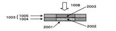
図1は、本発明の追記型光ディスクの実施形態の一例を示す模式的断面図である。図1に示した実施形態においては、基板1001の一主面上に、第1誘電体層1002、第1の反応層1004、第2の反応層1005、第2誘電体層1006及び保護層1007が順次積層されている。記録層1003は、第1の反応層1004と第2の反応層1005から成る。また、レーザ光1008は保護層1007の側から入射される場合を示している。 FIG. 1 is a schematic cross-sectional view showing an example of an embodiment of a write-once optical disc according to the present invention. In the embodiment shown in FIG. 1, a first
この基板1001の各層(第1誘電体層1002から保護層1007)が形成される側の一主面には、通常、情報の記録再生を行う際に光学スポットを導くための案内溝となる凹凸部(図示せず)が形成されている。この基板1001の厚さは、0.3mm〜1.2mmから選ばれることが好ましく、例えば、1.1mmに選ばれる。基板1001の材料としては、例えばポリカーボネート系樹脂、ポリオレフィン系樹脂及びアクリル系樹脂などのプラスチック材料や、ガラスなどが用いられる。 On one main surface of the
第1誘電体層1002及び第2誘電体層1006は、記録時において記録層1003が所定の出力を有するレーザ光で照射されたときに記録層1003で発生する熱が記録層1003の外部に放散されることを防止する。またこれらの層は、記録層1003がレーザ光で照射され加熱されたときに、記録層1003の熱変形を防止する。 The first
第1誘電体層1002及び第2誘電体層1006の構成材料は、透明な誘電体であれば特に限定されないが、記録再生用のレーザ光に対して、吸収能が低い材料から選ばれる。例えば、酸化物、硫化物、窒化物又はこれらを組み合わせたものを主成分として用いることができる。具体的には、例えば、Al2O3、AlN、ZnO、ZnS、GeN、GeCrN、CeO、SiO、SiO2、SiN及びSiC等から選択することが好ましい。モル比率が約4:1のZnS−SiO2混合体を主成分とすることがより好ましい。なお、第1誘電体層1002と第2誘電体層1006は、互いに同じ構成材料で構成されてもよいが、異なる構成材料で構成されてもよい。また、第1誘電体層1002及び第2誘電体層1006の層厚は光学設計により所望の値に設定されればよいため特に限定はされないが、5〜100nmであることが好ましい。この層厚を5nm以上にすれば、均一な厚さを有する誘電体層を形成することが容易になる。一方、層厚を100nm以下とすると、成膜時間が短くなり生産性が向上する。 The constituent material of the first
保護層1007は、追記型光ディスクを使用又は保存する際に、第2誘電体層1006又は記録層1003が損傷を受けないようにするための層である。また、記録時に記録層1003にレーザ光を照射する必要があるため、保護層1007は、光透過性を有する。従って、保護層1007の構成材料は光透過性を有していれば特に限定されない。例えば、保護層1007は、平面円環形状を有する光透過性シート(フィルム)と、この光透過性シートを第2誘電体層1006に貼り合わせるための接着層(共に図示せず)からなる光透過性カバーを用いて形成することができる。接着層は、例えば、紫外線硬化樹脂又は感圧性粘着剤からなる。光透過性シートは、記録/再生に用いられるレーザ光に対して、吸収能が低い材料からなることが好ましく、具体的には、光透過性シートの透過率を90%以上とすることのできる材料からなることが好ましい。具体的には、光透過性シートは、例えば、ポリカーボネート樹脂やポリオレフィン系樹脂からなる。光透過性シートは、例えば、ポリカーボネート樹脂やポリオレフィン系樹脂などの材料を押出機に投入し250〜300℃の押出温度で溶融して押し出し複数個の冷却ロールを用いてシート状に成形し、基板1001に合わせた形状に裁断することにより形成される。また、この光透過性シートの厚さは、3μm〜177μmの範囲内から選ばれることが好ましく、接着層との合計の厚さが例えば100μmになるように選ばれる。このような薄い保護層1007と、0.85程度の開口数(NAと表すことがある)を有する対物レンズとを組み合わせることによって、高密度記録を実現することができる。 The
また、保護層1007は、表面にゴミが付着したり、キズがついたりすることを防止する目的で、有機系あるいは無機系の材料からなる保護層をさらに有する光透過性カバーを用いて形成してもよい。この場合に使用する有機系又は無機系の材料も記録再生を行うレーザの波長に対して吸収能を殆ど有しないことが望ましい。 The
記録層1003は、第1の反応層1004と、これに隣接して配置された第2の反応層1005とを有している。この記録層1003は、記録時に所定の出力を有するレーザ光が基板又は保護層から入射され照射されたときに熱的影響により第1の反応層に含まれる水素量が減少し、その部分の光学的性質が変化することにより記録マークが形成される。この第1の反応層1004と、これに接触する第2の反応層1005とから成る記録層1003は、基板1001と保護層1007との間に配置されている。第1の反応層1004は、基板1001の側に配置され、第2の反応層1005は、保護層1007の側に配置されている。ここで、第1の反応層1004は、SiN、SiC又はSiO2を主成分とし、水素を含有する誘電体からなることが好ましい。また、第2の反応層1005は、第1の反応層より消衰係数が大きい材料からなる。消衰係数は大きいほど入射されたレーザ光を熱に変換しやすいことを意味する。従って、第2の反応層1005の主たる役割は、第1の反応層1004で起こる反応を助けるための熱の供与である。第2の反応層1005の消衰係数は、0.5以上であることが好ましく、Tb又はLaを主成分とする希土類金属や、Si又はAlを主成分とする金属、酸化物、窒化物、及び酸窒化物からなることが好ましい。この消衰係数は、使用する金属材料に大きく依存するが、その酸化物、窒化物、及び酸窒化物においては、成膜時の酸素ガス及び窒素ガスの導入量によって変更させることが可能である。また、光ディスクの多層化を考慮し高透過率な記録層1003を得る観点では、第2の反応層の消衰係数は3.3以下であることがより好ましい。 The
また、上記第1の反応層1004の主成分と、第2の反応層1005の主成分が、SiNとTb又はSiとの組み合わせとなるようにすることがさらに好ましい。更に、第2の反応層1005に希土類金属を用いた場合は、記録時以外における酸化或いは硫化に対する安定性を向上させる観点から、上述の主成分となる元素の他に、Mg、Ti、Cr、Ni、Al、Si、Ga、Ge等が添加されていてもよい。記録層1003の層厚は、記録時にレーザ光の照射を受けた第1の反応層1004の部分が速やかに水素の減少により光学的変化が生じた記録マーク2001(図2参照)を形成することができる厚さであれば特に限定されない。但し、記録層1003の層厚を薄くすることで、記録マークの形成がより短時間で進行し、高速記録を行うことがより容易に可能となる。また、第1の反応層1004と第2の反応層1005との層厚比率も特に限定はされないが、第2の反応層1005としてTb、La、Si、Alの金属元素を主成分とする層で構成した場合、多層化する際には透過率の観点を考慮して5〜10nmとすることが好ましい。 More preferably, the main component of the
次に、上記追記型光ディスクの製造方法の一例について説明する。
基板1001上に配置される第1誘電体層1002から第2誘電体層1006までの各層は、夫々の層の構成元素を含む化学種を用いた気相成長法により形成することができる。このような気相成長法としては、例えば、真空蒸着法、スパッタリング法、プラズマCVD法等が挙げられる。そして、第2誘電体層1006上に保護層1007を形成する。保護層1007は、上述した光透過性カバーを張り合わせる方法により形成することができる。またこれ以外にも、例えば、アクリル系又はエポキシ系の紫外線硬化性樹脂を溶剤に溶解して樹脂溶液を作製し、スピンコート法等により塗布・乾燥し、硬化して形成することができる。こうして追記型光ディスクを製造することができる。Next, an example of a method for manufacturing the write-once optical disc will be described.
Each layer from the
なお、上記追記型光ディスクの製造方法は、上記製造方法に特に限定されるものではなく、公知の光ディスクの製造に採用されている製造技術を用いることができる。 Note that the method for manufacturing the write-once optical disc is not particularly limited to the above-described manufacturing method, and a manufacturing technique employed for manufacturing a known optical disc can be used.
次に、本発明の光記録方法について説明する。
本発明の光記録方法は、上述した追記型光ディスクに対して、所定の出力を有するレーザ光を基板又は保護層側から記録層に照射して該記録層を構成する第1の反応層の前記レーザ光が照射された領域において水素量の減少による光学的特性の変化を生じせしめることにより記録マークを形成するものである。Next, the optical recording method of the present invention will be described.
In the optical recording method of the present invention, the above-mentioned write-once optical disc is irradiated with laser light having a predetermined output from the substrate or the protective layer side to the recording layer, and the first reaction layer constituting the recording layer A recording mark is formed by causing a change in optical characteristics due to a decrease in the amount of hydrogen in a region irradiated with laser light.
本発明の光記録方法の実施形態として、上記本発明の追記型光ディスクを用い、所定の出力を有するレーザ光を保護層側から入射し該保護層に照射する光記録方法を例にして説明する。図1は、本発明における追記型光ディスクの第1の実施形態を示す模式的断面図である。図1に示すように、この追記型光ディスクに対して、所定の出力を有するレーザ光1008を保護層1007側から入射し記録層1003に照射する。すると、第2の反応層1005においては、照射された領域でレーザ光が吸収され、これによりこの領域の温度が300乃至700℃まで上昇し、図2に示すように、水素の解離/離脱が生じ含有水素が減少した第1の反応層の領域2002が形成される。この領域において、第1の反応層は、水素をほとんど含有していない誘電体層へと変化する。これにより、光学的変化が生じた記録マーク2001が形成されることとなる。他方、第2の反応層1005は、第1の反応層1004から離脱した水素を含む領域2003が形成されることとなる。特に、第2の反応層1005として、TbやLaの希土類金属を用いた場合、水素化物を形成し消衰係数が減少する。 As an embodiment of the optical recording method of the present invention, an optical recording method using the write-once optical disc of the present invention as described above and irradiating the protective layer with a laser beam having a predetermined output will be described as an example. . FIG. 1 is a schematic cross-sectional view showing a first embodiment of a write-once optical disc according to the present invention. As shown in FIG. 1, a
この記録前後における光学特性の変化を調べるために、ガラス基板上に第1の反応層1004と同条件にて作製したサンプルを、加熱炉で250℃、1h熱処理した。第1の反応層サンプルの熱処理前後の屈折率はガラス基板上に成膜したサンプルの反射率から算出した。1枚のサンプルについて任意の10ケ所の反射率を測定し、それから算出した屈折率の平均値をそのサンプルの屈折率とした。反射率の測定には、日本分光社製の分光光度計を用いた。得られた結果を表1に示す。 In order to examine the change in optical characteristics before and after recording, a sample prepared on the glass substrate under the same conditions as the

表1に示されているように、上記の条件で熱処理すると、第1の反応層サンプルの屈折率に増加が見られ、これにより記録未記録領域間で反射率差が充分に高く取れ、再生時に高い再生信号(C/N比)が得られることが分かる。 As shown in Table 1, when the heat treatment is performed under the above conditions, the refractive index of the first reaction layer sample is increased, and thus the difference in reflectance between recorded and unrecorded areas is sufficiently high, and reproduction is performed. It can be seen that sometimes a high reproduction signal (C / N ratio) is obtained.
一方、第2の反応層1005においてもレーザ光の照射部位において光学的特性の変化が生じる可能性がある。例えば、第2の反応層1005を希土類金属を主成分とする材料で構成した場合、第1の反応層1004から離脱した水素との反応で希土類金属の水素化物を形成し、その部分が略透明になる。このため、記録層の多層化においては、記録未記録領域間での透過率差が懸念される。しかし、第2の反応層の膜厚を5〜10nmとすれば、厚さが薄いため変化の割合は小さく、充分に無視出来うるものとなる。 On the other hand, also in the
記録マーク2001は、水素が解離/離脱して形成された化学量論組成近傍の誘電体膜から形成される。このため、記録マークの熱的安定性が高く、広範囲の再生パワーに適用が可能で、再生信号のC/N比の経時的な劣化が充分に防止される。従って、光記録後は、長期間にわたって記録情報の劣化が効果的に防止される。すなわち、記録時に得られる良好な初期の再生信号のC/N比が長期間にわたって維持され、再生信号の経時的劣化が十分に防止される。 The
(第2の実施形態)
図3は、本発明における追記型光ディスクの第2の実施形態を示す模式的断面図である。図3に示した第2の実施形態においては、基板1001と第1誘電体層1002との間に、レーザ光に対する反射率が記録層1003よりも高い反射層3001が更に配置されている以外は、図1に示した追記型光ディスクと同様の構成を有している。(Second Embodiment)
FIG. 3 is a schematic cross-sectional view showing a second embodiment of a write-once optical disc according to the present invention. In the second embodiment shown in FIG. 3, a
反射層3001を設けると、記録層1003への光記録後に再生光を入射する場合に、多重干渉効果により高い再生信号(C/N比)が得られやすくなる。この反射層3001の構成材料は、レーザ光に対する反射層3001の反射率を記録層1003よりも大きくすることができる限り特に制限されない。例えば、好ましい構成材料として、Mg、Al、Ti、Cr、Fe、Co、Ni、Cu、Zn、Ge、Ag、Pt、Au等を挙げることができる。これらのうち、高い反射率を有することから、Al、Au、Ag、Cu又はこれらの合金(例えば、AlとTa、Ti、Cr、Siとの合金等)などの金属材料がより好ましく用いられる。また、反射層3001の厚さは、通常、80nm以上140nm以下に選ばれることが好ましく、例えば100nmに選ばれる。反射層3001の厚さを80nm以上にすると、記録層1003において生じる熱がすみやかに拡散され、容易に冷却することができるようになり、再生時に再生パワーによりジッター特性が低下するのを抑えることができる。他方、反射層3001の厚さを140nm以下とすると、熱特性や光学的な特性に厚みの差に依存する差異が生じず、実用上好ましい。 When the
反射層3001は、例えば第1の実施形態における他の層と同様に、反射層3001の構成元素を含む化学種を用いた気相成長法により形成することができる。 The
また、この第2の実施形態の追記型光ディスクを用いる光記録方法は、第1の実施形態と同様にして行うことができる。但し、この追記型光ディスクは、反射層3001を備えるため、光記録後に再生光を入射する場合に、多重干渉効果により高い再生信号(C/N比)が得られやすくなる。 In addition, the optical recording method using the write-once optical disc of the second embodiment can be performed in the same manner as in the first embodiment. However, since this write-once optical disc includes the
(第3の実施形態)
図4は、本発明の追記型光ディスクの第3の実施形態を示す模式的断面図である。
図4に示した実施形態の追記型光ディスクは、第2誘電体層1006と保護層1007との間に、もう1層の記録層(第2記録層4004)を有するデュアルレイヤー構成の光ディスクである。第2記録層4004は、第3の反応層4005と第4の反応層4006からなる。ここで、基板1001から第2誘電体層1006までは、第2の実施形態と同構成のものである。この第2誘電体層1006上に中間層4001を設ける。中間層4001は、アクリル系又はエポキシ系の紫外線硬化性樹脂を溶剤に溶解して樹脂溶液を作製し、スピンコート法等により形成することができる。この中間層4001の各層(第2反射層4002から第4誘電体層4007)が形成される側の一主面には、情報の記録再生を行う際に光学スポットを導くための案内溝となる凹凸部(図示せず)が形成されている。この凹凸部は、例えば紫外線硬化樹脂による樹脂層を形成し、これに2P法(Photo-Polymerization法)によって形成することができる。(Third embodiment)
FIG. 4 is a schematic cross-sectional view showing a third embodiment of a write-once optical disc according to the present invention.
The write-once optical disk of the embodiment shown in FIG. 4 is an optical disk having a dual layer structure in which another recording layer (second recording layer 4004) is provided between the
この中間層4001の厚さは、記録層の総数により所望の値に決定されればよく、特に限定されないが、本実施形態のデュアルレイヤー構成の追記型光ディスクの場合、通常10μm以上40μm以下に選ばれることが好ましく、例えば25μmに選ばれる。また、中間層4001の上に形成される第2反射層4002、第3誘電体層4003、第2記録層4004及び第4誘電体層4007は、第2の実施形態に記載の反射層3001から第2誘電体層1006と同じ材料で構成されてよい。また、各々の層の厚さは光学設計によって所望の値が選ばれるため、特に限定されない。 The thickness of the
以上、本発明について好適な実施形態を例として挙げ説明したが、本発明は上記第1〜第3の実施形態に限定されるものではない。例えば、上記第1〜第3の実施形態においては、記録層1003において、第1の反応層1004が基板1001側に配置され、第2の反応層1005が保護層1007側に配置されている。これらの実施形態における配置を変えて、例えば、第1の反応層1004と第2の反応層1005の位置を入れ替えた構成としてもよい。また、記録再生時のレーザ光1008は、保護層1007側から入射し記録層1003(及び第2記録層4004)に照射する場合を示したが、基板1001側から入射し記録層1003(及び第2記録層4004)に照射する構成であってもよい。この場合、基板1001は光透過性を有していればよく、特に限定はされない。また、第1誘電体層と第2誘電体層(及び第3誘電体層と第4誘電体層)の間に記録層を配置する構成を有する追記型光ディスクについて説明したが、これら誘電体層を有しない構成を有する追記型光ディスクであってもよい。また、1つの誘電体層のみを、例えば、保護層と記録層との間に、又は、基板と記録層との間に配置した構成を有する追記型光ディスクであってもよい。 As mentioned above, although preferred embodiment was mentioned and demonstrated about this invention as an example, this invention is not limited to the said 1st-3rd embodiment. For example, in the first to third embodiments, in the
また、記録層が2層構造の追記型光ディスクについて説明したが、少なくとも1つの第1の反応層とこれに接触する少なくとも1つの第2の反応層を有するものであれば、2層以上の層から構成された記録層を有するものであってもよい。例えば、2つの第1の反応層と、2つの第1の反応層間に配置された第2の反応層とからなる3層構造の記録層を有するものであってもよい。 Further, the write-once type optical disk having a two-layer structure has been described. However, if the recording layer has at least one first reaction layer and at least one second reaction layer in contact with it, two or more layers are used. It may have a recording layer composed of For example, the recording layer may have a three-layer structure including two first reaction layers and a second reaction layer disposed between the two first reaction layers.
また、第3の実施形態として、デュアルレイヤー構成の追記型光ディスクを説明したが、3層以上の記録層を有する多層化構成の追記型光ディスクであってもよい。 Further, the write-once optical disc having the dual layer configuration has been described as the third embodiment, but a write-once optical disc having a multi-layer configuration having three or more recording layers may be used.
以下に実施例を示し、本発明を更に詳細に説明するが、本発明はその主旨を逸脱しない限り、以下の実施例に限定されるものではない。 EXAMPLES Hereinafter, the present invention will be described in more detail with reference to examples. However, the present invention is not limited to the following examples without departing from the gist thereof.
(実施例1)
直流、RF、及びマイクロ波電源を有するプラズマCVDとマグネトロンスパッタリングの混合装置を用いて、基板上に、第1誘電体層、第1の反応層、第2の反応層、第2誘電体層および保護層を有する追記型光ディスクを作製した。基板としては、直径120mm、厚さ1.1mmのポリカーボネート基板を用いた。この基板の記録層を形成する側の一主面には、トラックピッチ(凹凸の繰り返し幅)が0.32μmのトラッキング用の案内溝(グルーブ、ランド)が形成されている。Example 1
Using a plasma CVD and magnetron sputtering mixing apparatus having direct current, RF, and microwave power sources, a first dielectric layer, a first reaction layer, a second reaction layer, a second dielectric layer, and A write-once optical disc having a protective layer was produced. As the substrate, a polycarbonate substrate having a diameter of 120 mm and a thickness of 1.1 mm was used. On one main surface of the substrate on the side where the recording layer is formed, a tracking guide groove (groove, land) having a track pitch (repetitive width of unevenness) of 0.32 μm is formed.
上記基板を基板ホルダーに固定した後、2×10⁻⁵Pa以下の高真空になるまでチャンバー内をクライオポンプで真空排気した。その後、真空排気したまま、まず、ArガスとO2ガスをチャンバー内に流しコンダクタンス調整により圧力を0.3Paに調節した。基板回転数100rpm、ターゲットへの投入パワー密度1.59W/cm2、Arガス100sccm、O2ガス1sccmの条件の下で、スパッタリング法で基板上に50nmの膜厚の第1誘電体層を成膜した。第1誘電体層は、SiO2を20mol%含有するZnS−SiO2混合体からなる層であった。ターゲットとして、SiO2を20mol%含有するZnSターゲットを用いた。After fixing the substrate to the substrate holder, the inside of the chamber was evacuated by a cryopump until a high vacuum of 2 × 10⁻⁵ Pa or less was reached. Thereafter, with the vacuum evacuated, first, Ar gas and O2 gas were flowed into the chamber, and the pressure was adjusted to 0.3 Pa by conductance adjustment. A first dielectric layer having a thickness of 50 nm is formed on the substrate by sputtering under the conditions of a substrate rotational speed of 100 rpm, a target power density of 1.59 W / cm2 , an Ar gas of 100 sccm, and an O2 gas of 1 sccm. Filmed. The first dielectric layer was a layer made of ZnS-SiO2 mixture containing SiO2 20 mol%. As a target, a ZnS target containing 20 mol% of SiO2 was used.
次いで、別のチャンバーに基板を搬送し、SiH4ガス、N2ガスを導入し、マイクロ波プラズマCVD法を用いて第1の反応層1004の形成を行った。SiH4ガス、及びN2ガスをチャンバー内に流し、コンダクタンス調整により圧力を4Paに調整した。基板を回転しながら、第1の反応層1004として水素含有SiN層を25nm成膜した。第1の反応層1004の水素含有量は上記と同様の成膜条件でガラス基板上に成膜した水素含有SiN層サンプルの水素含有量を2次イオン質量分析装置(SIMS)により測定することにより求めた。第1の反応層1004の水素含有量は2.1×10²²atoms/cm3であった。また、膜応力は、応力測定用の直径30mm、厚さ1.0mmのガラス円板上に上記と全く同様の成膜条件で水素含有SiN層を成膜し、この基板の変形を干渉計を用いてニュートンリングの本数として検出し測定した。Next, the substrate was transferred to another chamber, SiH4 gas and N2 gas were introduced, and the
ここでニュートンリングの本数をmとすると、基板の曲率半径γは下式(1)で求めることができる。
γ=a2/mλ (1)
a:基板の半径
λ:干渉計使用光源の波長
ここでγの値を下式(2)に代入すると水素含有SiN膜の応力σが求められる。
σ=Eb2/6(1−ν)γd (2)
E:基板のヤング率
ν:基板のポアッソン比
γ:基板の曲率半径
d:SiN膜の厚さ
b:基板の厚さ
測定された第2の反応層の膜応力は−1.0kg/mm2(圧縮応力状態)であった。Here, when the number of Newton rings is m, the curvature radius γ of the substrate can be obtained by the following equation (1).
γ = a2 / mλ (1)
a: Radius of substrate λ: Wavelength of light source using interferometer Here, when the value of γ is substituted into the following equation (2), the stress σ of the hydrogen-containing SiN film is obtained.
σ = Eb 2/6 (1 -ν) γd (2)
E: Young's modulus of substrate ν: Poisson's ratio of substrate γ: radius of curvature of substrate d: thickness of SiN film b: thickness of substrate The measured film stress of the second reaction layer is −1.0 kg / mm2. (Compressive stress state).
プラズマCVDの成膜条件は次の通りである。
(1)ガス種類 SiH4、N2
(2)ガス圧力 4〜13 Pa
(3)流量
SiH4 200 sccm
N2 500 sccm
(4)投入パワー 1.5kw
なお、上記「sccm」は「standard cc/min」を表し、「1sccm」は、毎分1cm3の割合で、圧力1013hPa、温度0℃のガスが流れること示している。The film formation conditions for plasma CVD are as follows.
(1) Gas type SiH4 , N2
(2) Gas pressure 4-13 Pa
(3) Flow rate SiH4 200 sccm
N2 500 sccm
(4) Input power 1.5 kW
The “sccm” represents “standard cc / min”, and “1 sccm” indicates that a gas having a pressure of 1013 hPa and a temperature of 0 ° C. flows at a rate of 1 cm3 per minute.
その後、別のチャンバーに基板を搬送しArガスを導入し、コンダクタンス調整により圧力を0.6Paに調整した。基板回転数50rpm、ターゲットへの投入パワー密度3.79W/cm2の条件の下で、第2の反応層1005としてTb層を5nmスパッタリング法で基板上に成膜した。第2の反応層の成膜時にO2ガス及びN2ガスが混入すると酸や窒化などを起こし易く水素化特性に影響を与えるため、第2の反応層は、このように、その他の層を形成するチャンバーとは別のチャンバーにて成膜を行った。また、第2の反応層に用いたTb層の消衰係数は、上記と同様の成膜条件でシリコンウエハ上に成膜したTb膜を分光エリプソメーターを用いて測定し求めた。その結果、本実施例に用いた第2の反応層Tb膜の消衰係数は、3.0であった。Thereafter, the substrate was transported to another chamber, Ar gas was introduced, and the pressure was adjusted to 0.6 Pa by conductance adjustment. A Tb layer was formed as a
その後、別のチャンバーに基板を搬送して、ArガスとO2ガスをチャンバー内に流しコンダクタンス調整により圧力を0.3Paに調整した。基板回転数100rpm、ターゲットへの投入パワー密度1.59W/cm2、Arガス100sccm、O2ガス1sccmの条件の下で、スパッタリング法で基板上に45nmの層厚を有する第2誘電体層を成膜した。第2誘電体層は、SiO2を20mol%含有するZnS−SiO2混合体からなる層であった。ターゲットとして、SiO2を20mol%含有するZnSターゲットを用いた。Thereafter, the substrate was transported to another chamber, Ar gas and O2 gas were allowed to flow into the chamber, and the pressure was adjusted to 0.3 Pa by conductance adjustment. A second dielectric layer having a layer thickness of 45 nm is formed on the substrate by sputtering under the conditions of a substrate rotation speed of 100 rpm, a target power density of 1.59 W / cm2 , an Ar gas of 100 sccm, and an O2 gas of 1 sccm. A film was formed. Second dielectric layer was a layer made of ZnS-SiO2 mixture containing SiO2 20 mol%. As a target, a ZnS target containing 20 mol% of SiO2 was used.
上記のようにして、各層を形成した後、直流、RF及びマイクロ波電源を有するプラズマCVDとマグネトロンスパッタリングの混合装置から取り出し、最後に保護層として、光透過性カバーを第2誘電体層上に積層し追記型光ディスクを得た。光透過性カバーは、径22mmの中心孔を有する外形120mmの平面円環形状を有する厚さ80μmの光透過性シートの一主面に予め均一に感圧性粘着剤(PSA)からなる接着層を20μmの厚さに塗布して作製した。 After each layer is formed as described above, it is taken out from a plasma CVD and magnetron sputtering mixing apparatus having direct current, RF and microwave power sources, and finally a light-transmitting cover is formed on the second dielectric layer as a protective layer. A laminated write-once optical disk was obtained. The light-transmitting cover has an adhesive layer made of a pressure-sensitive adhesive (PSA) uniformly in advance on one main surface of a light-transmitting sheet having a planar annular shape with an outer diameter of 120 mm having a center hole with a diameter of 22 mm and a thickness of 80 μm. It was prepared by coating to a thickness of 20 μm.
次に、シバソク社製LM330A(商品名)を用い、このようにして作製した、上記本実施例の追記型光ディスクに対して、光透過性カバー側から、照射光を対物レンズによって集光させ、記録層を照射して、一般的な条件で、記録情報の記録及び再生を行った。ここで、照射光の波長λは、405nmとし、対物レンズのNAは、0.85、線速度は4.917m/s、記録信号は(1−7)RLL変調におけるビット長111.75nmのランダム信号とした。 Next, using the LM330A (trade name) manufactured by Shiba-Sok, the irradiation light was condensed from the light-transmitting cover side by the objective lens on the write-once optical disc of the above-described example, Recording information was recorded and reproduced under general conditions by irradiating the recording layer. Here, the wavelength λ of the irradiation light is 405 nm, the NA of the objective lens is 0.85, the linear velocity is 4.917 m / s, and the recording signal is random with a bit length of 111.75 nm in (1-7) RLL modulation. Signal.
その結果、ジッタ(σ/T)で8.0%と良好な値が得られた。また、H/H環境(80℃/90%)で、1,000時間の耐久試験を行ったところ、ジッタ(σ/T)で8.5%であり、特に大きなジッタ値の悪化は見られなかった。 As a result, a good value of 8.0% in jitter (σ / T) was obtained. In addition, when a durability test for 1,000 hours was performed in an H / H environment (80 ° C./90%), the jitter (σ / T) was 8.5%, and a particularly large deterioration in jitter value was observed. There wasn't.
(実施例2)
第1の反応層1004として、水素含有SiC層を下記条件で成膜した以外は実施例1と同様にして追記型光ディスクを作製し、実施例1と同様にして評価した。(Example 2)
As a
第1の反応層の水素含有量は3.0×10²²atoms/cm3、膜応力は−1.5kg/mm2(圧縮応力状態)であった。The hydrogen content of the first reaction layer was 3.0 × 10²² atoms / cm3 , and the film stress was −1.5 kg / mm2 (compressive stress state).
また、プラズマCVDの製膜条件は次の通りである。
(1)ガス種類 SiH4、C2H2
(2)ガス圧力 4〜13 Pa
(3)流量
SiH4 200 sccm
C2H2 200 sccm
(4)投入パワー 1.5kw
本実施例の追記型光ディスクにおいては、ジッタ(σ/T)で9.0%と、良好な値が得られた。また、H/H環境(80℃/90%)で、1,000時間の耐久試験では、ジッタ(σ/T)で9.8%であり、特に大きなジッタ値の悪化は見られなかった。The film formation conditions for plasma CVD are as follows.
(1) Gas type SiH4 , C2 H2
(2) Gas pressure 4-13 Pa
(3) Flow rate SiH4 200 sccm
C2 H2 200 sccm
(4) Input power 1.5 kW
In the write-once optical disc of this example, a good value of 9.0% was obtained in jitter (σ / T). Further, in an endurance test for 1,000 hours in an H / H environment (80 ° C./90%), the jitter (σ / T) was 9.8%, and no significant deterioration of the jitter value was observed.
(実施例3)
第1の反応層1004として、水素含有SiO2層を下記条件で成膜した以外は実施例1と同様にして追記型光ディスクを作製し、実施例1と同様にして評価した。(Example 3)
As a
第1の反応層1004の水素含有量は2.6×10²²atoms/cm3、膜応力は−0.5kg/mm2(圧縮応力状態)であった。The hydrogen content of the
また、プラズマCVDの製膜条件は次の通りである。
(1)ガス種類 SiH4、O2
(2)ガス圧力 4〜13 Pa
(3)流量
SiH4 200 sccm
O2 500 sccm
(4)投入パワー 1.5kwThe film formation conditions for plasma CVD are as follows.
(1) Gas type SiH4 , O2
(2) Gas pressure 4-13 Pa
(3) Flow rate SiH4 200 sccm
O2 500 sccm
(4) Input power 1.5 kW
本実施例の光ディスクにおいては、ジッタ(σ/T)で8.5%と、良好な値が得られた。また、H/H環境(80℃/90%)で、1,000時間の耐久試験では、ジッタ(σ/T)で9.1%であり、特に大きなジッタ値の悪化は見られなかった。 In the optical disk of this example, a good value of 8.5% was obtained in jitter (σ / T). Further, in a 1000 hours endurance test in an H / H environment (80 ° C./90%), the jitter (σ / T) was 9.1%, and no significant deterioration of the jitter value was observed.
(実施例4)
基板と第1誘電体層の間に80nmの厚さを有するAg合金(Au、Pt、Pd、In、Nd、Yが1mol%未満含有されたAg合金)からなる反射層をスパッタリング法により設けた。そして、第1誘電体層の厚さを10nmとした以外は実施例1と同様にして追記型光ディスクを作製し、実施例1と同様にして評価した。
本実施例の追記型光ディスクにおいては、ジッタ(σ/T)で7.0%と、良好な値が得られた。また、H/H環境(80℃/90%)で、1,000時間の耐久試験では、ジッタ(σ/T)で7.7%であり、特に大きなジッタ値の悪化は見られなかった。Example 4
A reflective layer made of an Ag alloy (Ag alloy containing less than 1 mol% of Au, Pt, Pd, In, Nd, and Y) having a thickness of 80 nm is provided between the substrate and the first dielectric layer by a sputtering method. . A write-once optical disc was produced in the same manner as in Example 1 except that the thickness of the first dielectric layer was set to 10 nm, and evaluated in the same manner as in Example 1.
In the write-once optical disc of this example, a good value of 7.0% was obtained in jitter (σ / T). Further, in an endurance test for 1,000 hours in an H / H environment (80 ° C./90%), the jitter (σ / T) was 7.7%, and no significant deterioration of the jitter value was observed.
(実施例5)
第2の反応層1005をLa層とした以外は実施例4と同様にして追記型光ディスクを作製し、評価した。第2の反応層の成膜は、Arガスを導入し、コンダクタンス調整により圧力を0.6Paに調整した。基板回転数50rpm、ターゲットへの投入パワー密度3.79W/cm2の条件の下で行った。また、本実施例の第2の反応層に用いたLa層の消衰係数は、3.3であった。
本実施例の追記型光ディスクにおいては、ジッタ(σ/T)で7.0%と、良好な値が得られた。また、H/H環境(80℃/90%)で、1,000時間の耐久試験では、ジッタ(σ/T)で7.8%であり、特に大きなジッタ値の悪化は見られなかった。(Example 5)
A write-once optical disc was fabricated and evaluated in the same manner as in Example 4 except that the
In the write-once optical disc of this example, a good value of 7.0% was obtained in jitter (σ / T). Further, in an endurance test for 1,000 hours in an H / H environment (80 ° C./90%), the jitter (σ / T) was 7.8%, and no significant deterioration of the jitter value was observed.
(実施例6)
第2の反応層1005として、Si層を形成した以外は実施例1と同様にして追記型光ディスクを作製し、実施例1と同様にして評価した。第2の反応層の成膜は、Arガスを導入し、コンダクタンス調整により圧力を0.25Paに調整した。基板回転数50rpm、ターゲットへの投入パワー密度3.28W/cm2の条件の下で行った。また、第2の反応層に用いたSi層の消衰係数は、1.9であった。
本実施例の追記型光ディスクにおいては、ジッタ(σ/T)で6.8%と、良好な値が得られた。また、H/H環境(80℃/90%)で、1,000時間の耐久試験では、ジッタ(σ/T)で7.5%であり、特に大きなジッタ値の悪化は見られなかった。(Example 6)
A write-once optical disc was produced in the same manner as in Example 1 except that an Si layer was formed as the
In the write-once optical disc of this example, a good value of 6.8% in jitter (σ / T) was obtained. Further, in an endurance test for 1,000 hours in an H / H environment (80 ° C./90%), the jitter (σ / T) was 7.5%, and no significant deterioration of the jitter value was observed.
(実施例7)
第2の反応層1005として、SiON層を形成した以外は実施例1と同様にして追記型光ディスクを作製し、実施例1と同様にして評価した。第2の反応層の成膜は、Arガス、N2ガス、及びO2ガスを導入し、コンダクタンス調整により圧力を0.25Paに調整した。基板回転数50rpm、ターゲットへの投入パワー密度3.28W/cm2の条件の下で行った。また、第2の反応層に用いたSiON層の消衰係数は、0.5であった。
本実施例の追記型光ディスクにおいては、ジッタ(σ/T)で7.0%と、良好な値が得られた。また、H/H環境(80℃/90%)で、1,000時間の耐久試験では、ジッタ(σ/T)で7.9%であり、特に大きなジッタ値の悪化は見られなかった。(Example 7)
A write-once optical disc was produced in the same manner as in Example 1 except that a SiON layer was formed as the
In the write-once optical disc of this example, a good value of 7.0% was obtained in jitter (σ / T). Further, in an endurance test for 1,000 hours in an H / H environment (80 ° C./90%), the jitter (σ / T) was 7.9%, and no significant deterioration of the jitter value was observed.
(実施例8)
第2誘電体層と保護層との間に、中間層、第2反射層、第3誘電体層、第3の反応層と第4の反応層からなる第2記録層及び第4誘電体層の順で各層を更に設けた以外は、実施例5と同様にして追記型光ディスクを作製し、評価した。(Example 8)
Between the second dielectric layer and the protective layer, an intermediate layer, a second reflective layer, a third dielectric layer, a second recording layer comprising a third reaction layer and a fourth reaction layer, and a fourth dielectric layer A write-once optical disc was produced and evaluated in the same manner as in Example 5 except that each layer was further provided in this order.
上記各層は次のようにして作製した。
中間層は、エポキシ系の紫外線硬化性樹脂を溶剤に溶解して樹脂溶液を調製し、これをスピンコート法等によりコートし25μmの膜厚を有するものを形成した。中間層4001の第2反射層側一主面上には、紫外線硬化性樹脂を用いて2P法(Photo-Polymerization法)により、トラックピッチが320μmのトラッキング用の案内溝を形成した。Each of the above layers was produced as follows.
The intermediate layer was prepared by dissolving an epoxy-based ultraviolet curable resin in a solvent to prepare a resin solution, which was coated by a spin coating method or the like and having a film thickness of 25 μm. On one main surface of the
上記中間層の形成後、ディスクを再度、成膜装置内に戻し、2×10⁻⁵Pa以下の高真空になるまでチャンバー内をクライオポンプで真空排気した。その後、中間層上に、第2反射層として10nmの厚さのAg合金(Au、Pt、Pd、In、Nd、Yが1mol%未満含有されたAg合金)層をディスクを回転しながらスパッタリング法により成膜した。After the formation of the intermediate layer, the disk was returned to the film forming apparatus again, and the inside of the chamber was evacuated with a cryopump until a high vacuum of 2 × 10⁻⁵ Pa or less was reached. Then, a 10 nm thick Ag alloy (Ag alloy containing less than 1 mol% of Au, Pt, Pd, In, Nd, and Y) as a second reflective layer on the intermediate layer is sputtered while rotating the disk. Was formed.
次いで、ArガスとO2ガスをチャンバー内に流しコンダクタンス調整により圧力を0.3Paに調整した。基板回転数100rpm、ターゲットへの投入パワー密度1.59W/cm2、Arガス100sccm、O2ガス1sccmの条件の下で、スパッタリング法で第2反射層上に、30nmの層厚を有する第3誘電体層を成膜した。第3誘電体層は、SiO2を20mol%含有するZnS−SiO2混合体からなる層であった。ターゲットとして、SiO2を20mol%含有するZnSターゲットを用いた。Next, Ar gas and O2 gas were flowed into the chamber, and the pressure was adjusted to 0.3 Pa by conductance adjustment. A third layer having a layer thickness of 30 nm is formed on the second reflective layer by sputtering under the conditions of a substrate rotational speed of 100 rpm, a target power density of 1.59 W / cm2 , an Ar gas of 100 sccm, and an O2 gas of 1 sccm. A dielectric layer was formed. The third dielectric layer was a layer made of ZnS-SiO2 mixture containing SiO2 20 mol%. As a target, a ZnS target containing 20 mol% of SiO2 was used.
次いで、別のチャンバーにディスクを搬送して、SiH4ガス、N2ガスをチャンバー内に流しコンダクタンス調整により圧力を4Paに調整した。ディスクを回転しながら、プラズマCVD法を用いて、第3の反応層として水素含有SiN層を25nm成膜した。得られた第3の反応層の水素含有量を実施例1に記載の方法で測定した。第3の反応層の水素含有量は2.1×10²²atoms/cm3であった。プラズマCVDの成膜条件は次の通りであった。
(1)ガス種類 SiH4、N2
(2)ガス圧力 4〜13 Pa
(3)流量
SiH4 200 sccm
N2 500 sccm
(4)投入パワー 1.5kwNext, the disk was transported to another chamber, SiH4 gas and N2 gas were allowed to flow into the chamber, and the pressure was adjusted to 4 Pa by conductance adjustment. While rotating the disk, a hydrogen-containing SiN layer having a thickness of 25 nm was formed as a third reaction layer by plasma CVD. The hydrogen content of the obtained third reaction layer was measured by the method described in Example 1. The hydrogen content of the third reaction layer was 2.1 × 10²² atoms / cm3 . The plasma CVD film forming conditions were as follows.
(1) Gas type SiH4 , N2
(2) Gas pressure 4-13 Pa
(3) Flow rate SiH4 200 sccm
N2 500 sccm
(4) Input power 1.5 kW
その後、別のチャンバーに基板を搬送しArガスを導入し、コンダクタンス調整により圧力を0.6Paに調整した。基板回転数50rpm、ターゲットへの投入パワー密度3.79W/cm2の条件の下で、第4の反応層としてTb層を5nmスパッタリング法で第3の反応層上に成膜した。この層の消衰係数は実施例1同様、3.0であった。Thereafter, the substrate was transported to another chamber, Ar gas was introduced, and the pressure was adjusted to 0.6 Pa by conductance adjustment. A Tb layer was formed as a fourth reaction layer on the third reaction layer by a 5 nm sputtering method under the conditions of a substrate rotation speed of 50 rpm and an input power density of 3.79 W / cm2 to the target. The extinction coefficient of this layer was 3.0 as in Example 1.
その後、別のチャンバーにディスクを搬送して、ArガスとO2ガスをチャンバー内に流しコンダクタンス調整により圧力を0.3Paに調整した。基板回転数100rpm、ターゲットへの投入パワー密度1.59W/cm2、Arガス100sccm、O2ガス1sccmの条件の下で、スパッタリング法で45nmの厚さを有する第4誘電体層を第4の反応層上に成膜した。第4誘電体層は、SiO2を20mol%含有するZnS−SiO2混合体からなる層であった。Thereafter, the disk was transported to another chamber, Ar gas and O2 gas were allowed to flow into the chamber, and the pressure was adjusted to 0.3 Pa by conductance adjustment. A fourth dielectric layer having a thickness of 45 nm is formed by a sputtering method under conditions of a substrate rotation speed of 100 rpm, a target power density of 1.59 W / cm2 , an Ar gas of 100 sccm, and an O2 gas of 1 sccm. A film was formed on the reaction layer. The fourth dielectric layer was a layer made of ZnS-SiO2 mixture containing SiO2 20 mol%.
本実施例の追記型光ディスクにおいては、基板側に配置された記録層では、ジッタ(σ/T)で7.0%、保護層側に配置された第2記録層では、ジッタ(σ/T)で8.5%と良好な結果が得られた。また、H/H環境(80℃/90%)で、1,000時間の耐久試験では、基板側に配置された記録層で、ジッタ(σ/T)で7.8%、保護層側に配置された第2記録層で、ジッタ(σ/T)で9.4%であった。このように何れの記録層においても特に大きなジッタ値の悪化は見られなかった。 In the write-once optical disc of this example, the recording layer arranged on the substrate side has 7.0% jitter (σ / T), and the second recording layer arranged on the protective layer side has jitter (σ / T). ) Gave a good result of 8.5%. Further, in an endurance test of 1,000 hours in an H / H environment (80 ° C./90%), the recording layer disposed on the substrate side has a jitter (σ / T) of 7.8% and the protective layer side. In the second recording layer, the jitter (σ / T) was 9.4%. Thus, no significant deterioration of the jitter value was observed in any recording layer.
(比較例1)
比較例1では、第2の反応層1005として、成膜条件を変えてSiON層を形成した以外は実施例7と同様にして追記型光ディスクを作製し、実施例1と同様にして評価した。第2の反応層の成膜は、Arガス、N2ガス、及びO2ガスを導入し、コンダクタンス調整により圧力を0.25Paに調整した。その際、導入したN2ガス及びO2ガスは、Arガス、N2ガス、及びO2ガスのトータルガス流量に対する比率を変更(増加)して成膜を行った。また、基板の回転数は50rpm、ターゲットへの投入パワー密度は3.28W/cm2の条件の下で行った。
本比較例の第2の反応層に用いたSiON層の消衰係数は、0.3であった。
本比較例の追記型光ディスクにおいては、記録パワーに対する感度が悪く、ピークパワー15.0mWの記録でもジッタ(σ/T)が飽和せず16.7%と悪かった。よって、H/H環境(80℃/90%)における1,000時間の耐久試験は行わなかった。(Comparative Example 1)
In Comparative Example 1, a write-once optical disc was produced in the same manner as in Example 7 except that the SiON layer was formed by changing the film formation conditions as the
The extinction coefficient of the SiON layer used for the second reaction layer of this comparative example was 0.3.
In the write-once optical disc of this comparative example, the sensitivity to the recording power was poor, and the jitter (σ / T) did not saturate even when recording at a peak power of 15.0 mW, which was 16.7%. Therefore, the durability test for 1,000 hours in the H / H environment (80 ° C./90%) was not performed.
(比較例2)
比較例2では、第4の記録層4006として、NiCr層を3nm形成した以外は実施例8と同様にして追記型光ディスクを作製し、評価した。第4の記録層4006の成膜は、NiとCrの二種類のターゲットを用いた二元同時スパッタリングにて、夫々のターゲットへの投入パワーを制御することにより組成の調整を行った。本比較例では、Ni及びCrターゲットへの投入パワー密度は、夫々2.17W/cm2及び3.28W/cm2の条件の下で行った。その結果、本比較例の第4の記録層における組成はNi40Cr60at%であった。
また、圧力はArガスを導入しコンダクタンスの調整により0.5Paに調整し、基板の回転数は50rpmで行った。
本比較例の第4の記録層4006に用いたNiCr層の消衰係数は、3.5であった。(Comparative Example 2)
In Comparative Example 2, a write-once optical disc was manufactured and evaluated in the same manner as in Example 8 except that a 3 nm NiCr layer was formed as the
The pressure was adjusted to 0.5 Pa by introducing Ar gas and adjusting the conductance, and the rotation speed of the substrate was 50 rpm.
The extinction coefficient of the NiCr layer used for the
また、第4の記録層4006の膜厚を3nmと実施例8における5nmに対して薄くすることで、消衰係数増加による透過率の低下分を補償し、2層媒体用の記録層とした。このときの保護層側に配置される第2記録層側の膜の透過率は50%であった。 Further, by reducing the thickness of the
本比較例の追記型光ディスクにおいては、基板側に配置された記録層では、ジッタ(σ/T)で7.0%の値が得られたが、保護層側に配置された第2記録層では記録パワーに対する感度が悪く、ピークパワー15.0mWの記録でもジッタ(σ/T)が飽和せず18.4%と悪かった。よって、H/H環境(80℃/90%)における1,000時間の耐久試験は行わなかった。 In the write-once optical disc of this comparative example, the recording layer disposed on the substrate side obtained a value of 7.0% in jitter (σ / T), but the second recording layer disposed on the protective layer side. However, the sensitivity to the recording power was poor, and the jitter (σ / T) did not saturate even when recording with a peak power of 15.0 mW, which was 18.4%. Therefore, a 1,000 hour endurance test in an H / H environment (80 ° C./90%) was not performed.
本発明によれば、記録密度が高く、記録情報の保存安定性、並びに、ジッタ特性に優れ、多層化に好適な新規構成の追記型光ディスクの提供が可能である。 According to the present invention, it is possible to provide a write-once optical disc having a new configuration that has a high recording density, excellent recording information storage stability, jitter characteristics, and is suitable for multilayering.
1001 基板
1002 第1誘電体層
1003 記録層
1004 第1の反応層
1005 第2の反応層
1006 第2誘電体層
1007 保護層
1008 レーザ光
2001 記録マーク
2002 含有水素が減少した第1の反応層の領域
2003 水素を含む第2の反応層の領域
3001 反射層
4001 中間層
4002 第2反射層
4003 第3誘電体層
4004 第2記録層
4005 第3の反応層
4006 第4の反応層
4007 第4誘電体層1001
Claims (6)
Translated fromJapanese間に配置され、記録時に前記基板又は前記保護層側から入射されるレーザ光により前記記
録層の所定領域に記録マークを形成して記録を行う追記型光ディスクにおいて、
前記記録層が第1の反応層と第2の反応層との少なくとも2層から成り、且つ、該第1の反応層が水素を含有する材料からなり、該第2の反応層が前記第1の反応層より消衰係数が大である材料からなることを特徴とする追記型光ディスク。At least a substrate has a protective layer and a recording layer, the recording layer is disposed between the substrate and the protective layer, and the recording is performed by laser light incident from the substrate or the protective layer side during recording. In a write-once optical disc for recording by forming a recording mark in a predetermined area of a layer,
The recording layer is composed of at least two layers of a first reaction layer and a second reaction layer, the first reaction layer is composed of a material containing hydrogen, and the second reaction layer is the first reaction layer. A write-once optical disc comprising a material having an extinction coefficient larger than that of the reaction layer.
の間に設けられる第1誘電体層とが更に備えられていることを特徴とする請求項1乃至3のいずれかに記載の追記型光ディスク。2. The apparatus according to claim 1, further comprising: a second dielectric layer provided between the protective layer and the recording layer; and a first dielectric layer provided between the substrate and the recording layer. The write-once optical disc according to any one of items 1 to 3.
Priority Applications (2)
| Application Number | Priority Date | Filing Date | Title |
|---|---|---|---|
| JP2006279961AJP2007157314A (en) | 2005-11-10 | 2006-10-13 | Write-once optical disc and optical recording method |
| US11/557,831US7615333B2 (en) | 2005-11-10 | 2006-11-08 | Write-once optical disk and optical recording method |
Applications Claiming Priority (2)
| Application Number | Priority Date | Filing Date | Title |
|---|---|---|---|
| JP2005326172 | 2005-11-10 | ||
| JP2006279961AJP2007157314A (en) | 2005-11-10 | 2006-10-13 | Write-once optical disc and optical recording method |
Publications (1)
| Publication Number | Publication Date |
|---|---|
| JP2007157314Atrue JP2007157314A (en) | 2007-06-21 |
Family
ID=38004087
Family Applications (1)
| Application Number | Title | Priority Date | Filing Date |
|---|---|---|---|
| JP2006279961AWithdrawnJP2007157314A (en) | 2005-11-10 | 2006-10-13 | Write-once optical disc and optical recording method |
Country Status (2)
| Country | Link |
|---|---|
| US (1) | US7615333B2 (en) |
| JP (1) | JP2007157314A (en) |
Cited By (2)
| Publication number | Priority date | Publication date | Assignee | Title |
|---|---|---|---|---|
| WO2010106946A1 (en) | 2009-03-17 | 2010-09-23 | ソニー株式会社 | Process for producing optical recording medium and optical recording medium |
| WO2010106945A1 (en) | 2009-03-17 | 2010-09-23 | ソニー株式会社 | Optical recording medium and process for producing same |
Families Citing this family (2)
| Publication number | Priority date | Publication date | Assignee | Title |
|---|---|---|---|---|
| JP2003317315A (en)* | 2002-04-19 | 2003-11-07 | Tdk Corp | Optical recording medium |
| CZ2010666A3 (en) | 2010-09-07 | 2012-01-04 | Northern Star Spol. S R. O. | Optical data recording medium |
Family Cites Families (20)
| Publication number | Priority date | Publication date | Assignee | Title |
|---|---|---|---|---|
| JPS5764596A (en)* | 1980-10-06 | 1982-04-19 | Fuji Photo Film Co Ltd | Heat mode recording material |
| JPS5933320B2 (en)* | 1981-04-03 | 1984-08-15 | 株式会社東芝 | optical information recording medium |
| US4379299A (en)* | 1981-04-06 | 1983-04-05 | North American Philips Corporation | Recording structure for direct read after write recording |
| DE3364607D1 (en)* | 1982-03-15 | 1986-08-28 | Toshiba Kk | Optical type information recording medium |
| EP0107913B1 (en)* | 1982-09-29 | 1988-06-22 | Kabushiki Kaisha Toshiba | Radiation-sensitive carrier body utilized as stamper structure |
| JP2815977B2 (en)* | 1990-05-25 | 1998-10-27 | 日本電信電話株式会社 | Protective film for optical recording media |
| JPH0495246A (en)* | 1990-08-10 | 1992-03-27 | Nippon Telegr & Teleph Corp <Ntt> | Magneto-optical recording medium and production thereof |
| JPH04134653A (en)* | 1990-09-26 | 1992-05-08 | Shin Etsu Chem Co Ltd | Magneto-optical recording medium |
| JPH0660458A (en)* | 1992-05-22 | 1994-03-04 | Nec Corp | Single plate optical disk and recording and reproducing method for the same |
| WO1996038758A1 (en)* | 1995-05-30 | 1996-12-05 | Philips Electronics N.V. | Switching device and the use thereof |
| WO1996038759A1 (en)* | 1995-05-30 | 1996-12-05 | Philips Electronics N.V. | Switching device and use thereof |
| WO1998028660A1 (en)* | 1996-12-20 | 1998-07-02 | Koninklijke Philips Electronics N.V. | Furnace for rapid thermal processing |
| US5843553A (en)* | 1997-07-29 | 1998-12-01 | Eastman Kodak Company | High performance media for optical recording |
| JP3697896B2 (en)* | 1998-01-23 | 2005-09-21 | 株式会社デンソー | Optical information recording medium and manufacturing method thereof |
| JP2000298875A (en)* | 1999-02-13 | 2000-10-24 | Sony Corp | Optical recording medium |
| JP2002542513A (en)* | 1999-04-20 | 2002-12-10 | コーニンクレッカ フィリップス エレクトロニクス エヌ ヴィ | Transmission / reflection switchable display device |
| US6802073B1 (en)* | 1999-06-11 | 2004-10-05 | Tosoh Corporation | Magneto-optical recording medium |
| TW497098B (en)* | 2000-11-04 | 2002-08-01 | Li-Shin Jou | Optical recording medium and recording method |
| US20040038080A1 (en)* | 2002-07-01 | 2004-02-26 | Tdk Corporation | Optical recording medium and method for recording data in the same |
| FR2884032B1 (en)* | 2005-03-29 | 2007-06-08 | Commissariat Energie Atomique | IRREVERSIBLE OPTICAL RECORDING MEDIUM BY FORMING BUBBLES HAVING LIMITED HEIGHT BY THE GENERANT GAS SOURCE |
- 2006
- 2006-10-13JPJP2006279961Apatent/JP2007157314A/ennot_activeWithdrawn
- 2006-11-08USUS11/557,831patent/US7615333B2/ennot_activeExpired - Fee Related
Cited By (3)
| Publication number | Priority date | Publication date | Assignee | Title |
|---|---|---|---|---|
| WO2010106946A1 (en) | 2009-03-17 | 2010-09-23 | ソニー株式会社 | Process for producing optical recording medium and optical recording medium |
| WO2010106945A1 (en) | 2009-03-17 | 2010-09-23 | ソニー株式会社 | Optical recording medium and process for producing same |
| US8557362B2 (en) | 2009-03-17 | 2013-10-15 | Sony Corporation | Optical recording medium and method for manufacturing the same |
Also Published As
| Publication number | Publication date |
|---|---|
| US20070104919A1 (en) | 2007-05-10 |
| US7615333B2 (en) | 2009-11-10 |
Similar Documents
| Publication | Publication Date | Title |
|---|---|---|
| KR100709931B1 (en) | Information recording medium and its manufacturing method | |
| US20020076646A1 (en) | Optical information medium and its use | |
| JP4136980B2 (en) | Multi-layer phase change information recording medium and recording / reproducing method thereof | |
| KR20040035564A (en) | Optical recording medium and method for manufacturing the same | |
| US20040105182A1 (en) | Optical information recording medium | |
| US20040027966A1 (en) | Optical recording/reproducing method and optical recording medium | |
| JP2007157314A (en) | Write-once optical disc and optical recording method | |
| JP5386374B2 (en) | Optical information recording medium and manufacturing method thereof | |
| US20030235134A1 (en) | Optical recording/reproducing method and optical recording medium | |
| JPWO2004032130A1 (en) | Optical information recording medium and manufacturing method thereof | |
| JP2003203383A (en) | Write-once/read-many type optical recording medium and optically recording method | |
| JP3908571B2 (en) | Optical information recording medium, manufacturing method thereof, and recording / reproducing method thereof | |
| KR101017004B1 (en) | Optical recording medium and its manufacturing method | |
| JP5298623B2 (en) | Write-once optical recording medium | |
| US20070076579A1 (en) | Optical storage medium | |
| US20070271576A1 (en) | Phase-change optical storage medium | |
| JP4397838B2 (en) | Multilayer phase change optical recording medium | |
| JP4086689B2 (en) | Optical information recording medium and manufacturing method thereof | |
| KR20050059098A (en) | Rewritable optical data storage medium and use of such a medium | |
| JP2006095821A (en) | Photorecording medium | |
| JPWO2010032348A1 (en) | Information recording medium and manufacturing method thereof | |
| JP2005302264A (en) | Phase change optical information recording medium and two-layer phase change optical information recording medium | |
| JP2007287291A (en) | Multilayer optical recording medium and initialization method of multilayer optical recording medium | |
| JP3608934B2 (en) | Optical recording medium and protective film for optical recording medium | |
| JP4322719B2 (en) | Optical information recording medium, method for producing the same, and sputtering target |
Legal Events
| Date | Code | Title | Description |
|---|---|---|---|
| A621 | Written request for application examination | Free format text:JAPANESE INTERMEDIATE CODE: A621 Effective date:20091013 | |
| A761 | Written withdrawal of application | Free format text:JAPANESE INTERMEDIATE CODE: A761 Effective date:20100201 |