JP2007149870A - Circuit board and manufacturing method therefor - Google Patents
Circuit board and manufacturing method thereforDownload PDFInfo
- Publication number
- JP2007149870A JP2007149870AJP2005340773AJP2005340773AJP2007149870AJP 2007149870 AJP2007149870 AJP 2007149870AJP 2005340773 AJP2005340773 AJP 2005340773AJP 2005340773 AJP2005340773 AJP 2005340773AJP 2007149870 AJP2007149870 AJP 2007149870A
- Authority
- JP
- Japan
- Prior art keywords
- insulating
- wiring pattern
- substrate
- circuit board
- resin
- Prior art date
- Legal status (The legal status is an assumption and is not a legal conclusion. Google has not performed a legal analysis and makes no representation as to the accuracy of the status listed.)
- Pending
Links
Images


Classifications
- H—ELECTRICITY
- H01—ELECTRIC ELEMENTS
- H01L—SEMICONDUCTOR DEVICES NOT COVERED BY CLASS H10
- H01L23/00—Details of semiconductor or other solid state devices
- H01L23/48—Arrangements for conducting electric current to or from the solid state body in operation, e.g. leads, terminal arrangements ; Selection of materials therefor
- H01L23/488—Arrangements for conducting electric current to or from the solid state body in operation, e.g. leads, terminal arrangements ; Selection of materials therefor consisting of soldered or bonded constructions
- H01L23/498—Leads, i.e. metallisations or lead-frames on insulating substrates, e.g. chip carriers
- H01L23/49822—Multilayer substrates
- H—ELECTRICITY
- H05—ELECTRIC TECHNIQUES NOT OTHERWISE PROVIDED FOR
- H05K—PRINTED CIRCUITS; CASINGS OR CONSTRUCTIONAL DETAILS OF ELECTRIC APPARATUS; MANUFACTURE OF ASSEMBLAGES OF ELECTRICAL COMPONENTS
- H05K1/00—Printed circuits
- H05K1/02—Details
- H05K1/0271—Arrangements for reducing stress or warp in rigid printed circuit boards, e.g. caused by loads, vibrations or differences in thermal expansion
- H—ELECTRICITY
- H05—ELECTRIC TECHNIQUES NOT OTHERWISE PROVIDED FOR
- H05K—PRINTED CIRCUITS; CASINGS OR CONSTRUCTIONAL DETAILS OF ELECTRIC APPARATUS; MANUFACTURE OF ASSEMBLAGES OF ELECTRICAL COMPONENTS
- H05K3/00—Apparatus or processes for manufacturing printed circuits
- H05K3/46—Manufacturing multilayer circuits
- H05K3/4688—Composite multilayer circuits, i.e. comprising insulating layers having different properties
- H—ELECTRICITY
- H01—ELECTRIC ELEMENTS
- H01L—SEMICONDUCTOR DEVICES NOT COVERED BY CLASS H10
- H01L23/00—Details of semiconductor or other solid state devices
- H01L23/48—Arrangements for conducting electric current to or from the solid state body in operation, e.g. leads, terminal arrangements ; Selection of materials therefor
- H01L23/488—Arrangements for conducting electric current to or from the solid state body in operation, e.g. leads, terminal arrangements ; Selection of materials therefor consisting of soldered or bonded constructions
- H01L23/498—Leads, i.e. metallisations or lead-frames on insulating substrates, e.g. chip carriers
- H01L23/49827—Via connections through the substrates, e.g. pins going through the substrate, coaxial cables
- H—ELECTRICITY
- H01—ELECTRIC ELEMENTS
- H01L—SEMICONDUCTOR DEVICES NOT COVERED BY CLASS H10
- H01L23/00—Details of semiconductor or other solid state devices
- H01L23/48—Arrangements for conducting electric current to or from the solid state body in operation, e.g. leads, terminal arrangements ; Selection of materials therefor
- H01L23/488—Arrangements for conducting electric current to or from the solid state body in operation, e.g. leads, terminal arrangements ; Selection of materials therefor consisting of soldered or bonded constructions
- H01L23/498—Leads, i.e. metallisations or lead-frames on insulating substrates, e.g. chip carriers
- H01L23/49866—Leads, i.e. metallisations or lead-frames on insulating substrates, e.g. chip carriers characterised by the materials
- H01L23/49894—Materials of the insulating layers or coatings
- H—ELECTRICITY
- H01—ELECTRIC ELEMENTS
- H01L—SEMICONDUCTOR DEVICES NOT COVERED BY CLASS H10
- H01L2924/00—Indexing scheme for arrangements or methods for connecting or disconnecting semiconductor or solid-state bodies as covered by H01L24/00
- H01L2924/0001—Technical content checked by a classifier
- H01L2924/0002—Not covered by any one of groups H01L24/00, H01L24/00 and H01L2224/00
- H—ELECTRICITY
- H05—ELECTRIC TECHNIQUES NOT OTHERWISE PROVIDED FOR
- H05K—PRINTED CIRCUITS; CASINGS OR CONSTRUCTIONAL DETAILS OF ELECTRIC APPARATUS; MANUFACTURE OF ASSEMBLAGES OF ELECTRICAL COMPONENTS
- H05K1/00—Printed circuits
- H05K1/02—Details
- H05K1/03—Use of materials for the substrate
- H05K1/0313—Organic insulating material
- H05K1/0353—Organic insulating material consisting of two or more materials, e.g. two or more polymers, polymer + filler, + reinforcement
- H05K1/0366—Organic insulating material consisting of two or more materials, e.g. two or more polymers, polymer + filler, + reinforcement reinforced, e.g. by fibres, fabrics
- H—ELECTRICITY
- H05—ELECTRIC TECHNIQUES NOT OTHERWISE PROVIDED FOR
- H05K—PRINTED CIRCUITS; CASINGS OR CONSTRUCTIONAL DETAILS OF ELECTRIC APPARATUS; MANUFACTURE OF ASSEMBLAGES OF ELECTRICAL COMPONENTS
- H05K2201/00—Indexing scheme relating to printed circuits covered by H05K1/00
- H05K2201/01—Dielectrics
- H05K2201/0183—Dielectric layers
- H05K2201/0191—Dielectric layers wherein the thickness of the dielectric plays an important role
- H—ELECTRICITY
- H05—ELECTRIC TECHNIQUES NOT OTHERWISE PROVIDED FOR
- H05K—PRINTED CIRCUITS; CASINGS OR CONSTRUCTIONAL DETAILS OF ELECTRIC APPARATUS; MANUFACTURE OF ASSEMBLAGES OF ELECTRICAL COMPONENTS
- H05K2201/00—Indexing scheme relating to printed circuits covered by H05K1/00
- H05K2201/02—Fillers; Particles; Fibers; Reinforcement materials
- H05K2201/0275—Fibers and reinforcement materials
- H05K2201/029—Woven fibrous reinforcement or textile
- Y—GENERAL TAGGING OF NEW TECHNOLOGICAL DEVELOPMENTS; GENERAL TAGGING OF CROSS-SECTIONAL TECHNOLOGIES SPANNING OVER SEVERAL SECTIONS OF THE IPC; TECHNICAL SUBJECTS COVERED BY FORMER USPC CROSS-REFERENCE ART COLLECTIONS [XRACs] AND DIGESTS
- Y10—TECHNICAL SUBJECTS COVERED BY FORMER USPC
- Y10T—TECHNICAL SUBJECTS COVERED BY FORMER US CLASSIFICATION
- Y10T428/00—Stock material or miscellaneous articles
- Y10T428/24—Structurally defined web or sheet [e.g., overall dimension, etc.]
- Y10T428/24802—Discontinuous or differential coating, impregnation or bond [e.g., artwork, printing, retouched photograph, etc.]
- Y10T428/24917—Discontinuous or differential coating, impregnation or bond [e.g., artwork, printing, retouched photograph, etc.] including metal layer
Landscapes
- Engineering & Computer Science (AREA)
- Microelectronics & Electronic Packaging (AREA)
- Manufacturing & Machinery (AREA)
- Physics & Mathematics (AREA)
- Condensed Matter Physics & Semiconductors (AREA)
- General Physics & Mathematics (AREA)
- Computer Hardware Design (AREA)
- Power Engineering (AREA)
- Production Of Multi-Layered Print Wiring Board (AREA)
- Structure Of Printed Boards (AREA)
Abstract
Description
Translated fromJapanese本発明は、絶縁部材を介して積層され、互いに電気的に接続される複数の配線パターンを備える回路基板及びこの回路基板の製造方法に関するものである。 The present invention relates to a circuit board including a plurality of wiring patterns that are stacked via an insulating member and are electrically connected to each other, and a method for manufacturing the circuit board.
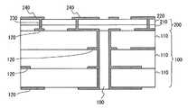
従来、実装される電子部品との熱膨張率差に起因して発生する応力の影響を低減する回路基板として特許文献1に示すものがあった。図5は、特許文献1に示す回路基板の概略構成を示す断面図である。 Conventionally, Patent Document 1 discloses a circuit board that reduces the influence of stress generated due to a difference in thermal expansion coefficient with a mounted electronic component. FIG. 5 is a cross-sectional view showing a schematic configuration of the circuit board shown in Patent Document 1. As shown in FIG.
特許文献1に示す回路基板は、本体部基板100とフィルム状基板200とを備える。本体部基板100は、絶縁性樹脂からなる絶縁層110と本体部配線パターン120とが積層されている。フィルム状基板200は、本体部基板100の一面側に接合されるものであり、ポリイミドなどの樹脂からなるフィルム220、フィルム220の一面側に形成された電子部品が実装される実装配線パターン240、本体部配線パターン120と実装配線パターン240とを電気的に接続するヴィア230、及び本体部基板100と実装配線パターン240との間に形成されるものであり、本体部基板100の絶縁層110よりも低弾性のNBRゴム分散型熱硬化性変性エポキシ樹脂シートなどの低弾性樹脂によって形成された低弾性樹脂層210を備える。 The circuit board shown in Patent Document 1 includes a
そして、特許文献1に示す回路基板は、低弾性樹脂層210が実装された電子部品と回路基板との熱膨張率に起因して発生する応力に対して容易に変形することによって、電子部品との熱膨張率差に起因して発生する応力を吸収又は緩和するものである。
しかしながら、特許文献1に示す回路基板においては、実装配線パターン240と本体部配線パターン120との間が樹脂シートなどで形成されているため、冷熱ストレスなどによって回路基板の表面にクラックが生じた場合、実装配線パターン240と本体部配線パターン120とが電気的に接続されフィルム状基板200における絶縁性が低下したり、本体部配線パターン120の断線が生じたりする可能性がある。 However, in the circuit board shown in Patent Document 1, since the space between the
また、特許文献1に示す回路基板においては、ビルドアップ法でしか製造できないため、微細加工が要求されない回路基板であっても製造工程が複雑になってしまう。 Moreover, since the circuit board shown in Patent Document 1 can be manufactured only by the build-up method, the manufacturing process becomes complicated even if the circuit board does not require fine processing.
本発明は、上記問題点に鑑みなされたものであり、絶縁部材における絶縁性の低下や配線パターンの断線などを防止しつつ実装される電子部品との熱膨張率差に起因して発生する応力の影響を低減する回路基板を提供することを第1の目的とし、回路基板を容易に製造することができる回路基板の製造方法を提供することを第2の目的とする。 The present invention has been made in view of the above problems, and stress generated due to a difference in thermal expansion coefficient from an electronic component to be mounted while preventing deterioration of insulation in an insulating member or disconnection of a wiring pattern. It is a first object to provide a circuit board that reduces the influence of the above, and a second object is to provide a circuit board manufacturing method that can easily manufacture a circuit board.
上記目的を達成するために請求項1に記載の回路基板は、補強基材及び絶縁性樹脂を有する絶縁部材を介して積層され、互いに電気的に接続される複数の配線パターンを備える回路基板であって、複数の配線パターンは、電気的接続部材を介して電子部品が実装される実装配線パターンと、実装配線パターンに対向する対向配線パターンとを備え、絶縁部材における実装配線パターンと対向配線パターンとの間の実装部絶縁部材は、回路基板の厚み方向において対向配線パターン側に偏った状態で補強基材が配置されることを特徴とするものである。 In order to achieve the above object, a circuit board according to claim 1 is a circuit board comprising a plurality of wiring patterns that are laminated via an insulating member having a reinforcing base and an insulating resin and are electrically connected to each other. The plurality of wiring patterns include a mounting wiring pattern on which an electronic component is mounted via an electrical connection member and a counter wiring pattern facing the mounting wiring pattern, and the mounting wiring pattern and the counter wiring pattern in the insulating member are provided. The mounting portion insulating member between the reinforcing substrate and the reinforcing portion is arranged in a state of being biased toward the opposing wiring pattern in the thickness direction of the circuit board.
このように、絶縁部材における実装配線パターンと対向配線パターンとの間の実装部絶縁部材は、回路基板の厚み方向において対向配線パターン側に偏った状態で補強基材を配置することによって、実装配線パターン側に樹脂のみの部分が存在し、対向配線パターン側に補強基材及び絶縁性樹脂を有する部分が存在するようにすることができる。 In this way, the mounting part insulating member between the mounting wiring pattern and the opposing wiring pattern in the insulating member is mounted on the mounting wiring by disposing the reinforcing substrate in a state of being biased toward the opposing wiring pattern in the thickness direction of the circuit board. It is possible to have a resin-only portion on the pattern side and a portion having a reinforcing base material and an insulating resin on the counter wiring pattern side.
この実装部絶縁部材の樹脂のみの部分は、補強基材と絶縁性樹脂からなる絶縁部材に比べて弾性率を低くすることができる。したがって、回路基板と電子部品との熱膨張率差に起因して応力が発生した場合であっても、この応力は、実装部絶縁部材の樹脂のみの部分が変形することによって緩和することができる。 The resin-only portion of the mounting portion insulating member can have a lower elastic modulus than an insulating member made of a reinforcing base material and an insulating resin. Therefore, even when stress is generated due to the difference in thermal expansion coefficient between the circuit board and the electronic component, this stress can be relaxed by deformation of the resin-only portion of the mounting portion insulating member. .
さらに、実装部絶縁部材の対向配線パターン側に補強基材を配置することによって、回路基板の表面にクラックが生じた場合であっても、対向配線パターン側に配置された補強基材によってクラックが対向配線パターンに達することを抑制することができる。したがって、実装部絶縁部材における絶縁性の低下や対向配線パターンの断線などを防止することができる。 Furthermore, even if a crack is generated on the surface of the circuit board by arranging the reinforcing base material on the opposing wiring pattern side of the mounting portion insulating member, the crack is caused by the reinforcing base material arranged on the opposing wiring pattern side. Reaching the counter wiring pattern can be suppressed. Therefore, it is possible to prevent a decrease in insulation in the mounting portion insulating member, disconnection of the opposing wiring pattern, and the like.
また、請求項2に記載の回路基板では、実装部絶縁部材における絶縁性樹脂と、絶縁部材における他の絶縁性樹脂とは同一材料からなることを特徴とするものである。 The circuit board according to claim 2 is characterized in that the insulating resin in the mounting portion insulating member and the other insulating resin in the insulating member are made of the same material.
このように、実装部絶縁部材における絶縁性樹脂と、絶縁部材における他の絶縁性樹脂とを同一材料とすることによって、絶縁部材における線膨張係数を同等にすることができるため、配線パターンへの応力を低減することができる。 In this way, by using the same material for the insulating resin in the mounting portion insulating member and the other insulating resin in the insulating member, the linear expansion coefficient in the insulating member can be made equal. Stress can be reduced.
また、請求項3に示すように、実装部絶縁部材における絶縁性樹脂は、絶縁部材における他の絶縁性樹脂に比べて弾性率を低くしてもよい。このように、実装部絶縁部材における絶縁性樹脂の弾性率を絶縁部材における他の絶縁性樹脂に比べて低くすることによって、回路基板と電子部品との熱膨張率差に起因して発生する応力による変形度合いを大きくすることができるため好適である。また、請求項4に示すように、実装部絶縁部材の樹脂部の絶縁性樹脂のみを他の絶縁性樹脂に比べて弾性率を低くするようにしてもよい。 According to a third aspect of the present invention, the insulating resin in the mounting portion insulating member may have a lower elastic modulus than other insulating resins in the insulating member. In this way, the stress generated due to the difference in thermal expansion coefficient between the circuit board and the electronic component by lowering the elastic modulus of the insulating resin in the mounting portion insulating member as compared with other insulating resins in the insulating member. It is preferable because the degree of deformation due to can be increased. According to a fourth aspect of the present invention, only the insulating resin of the resin portion of the mounting portion insulating member may have a lower elastic modulus than other insulating resins.
また、補強基材としては、請求項5及び請求項6に示すように、ガラスクロス、不繊布を用いることができる。 Moreover, as a reinforcement base material, as shown in Claim 5 and Claim 6, a glass cloth and a non-woven cloth can be used.
また、請求項7に記載の回路基板の製造方法では、補強基材及び絶縁性樹脂からなり配線パターンを有する絶縁性基板を含む複数の絶縁性基板と、補強基材及び絶縁性樹脂からなる補強基板と、絶縁性樹脂からなり電子部品が実装される実装配線パターンを有する樹脂基板とを備える回路基板の製造方法であって、絶縁性基板上に補強基板を積層し、樹脂基板を実装配線パターンの反対面が補強基板に対向した状態で補強基板上に積層する積層工程と、積層工程にて積層した絶縁性基板、補強基板、樹脂基板を一括で接着する接着工程と、接着工程後に、絶縁性基板、補強基板、樹脂基板に一括でスルーホールを形成し、実配線パターンと配線パターン、及び配線パターン間を電気的に接続する接続部材を一括でスルーホールに形成する接続部材形成工程とを備えることを特徴とするものである。 In the method for manufacturing a circuit board according to claim 7, a plurality of insulating substrates including an insulating substrate made of a reinforcing base material and an insulating resin and having a wiring pattern, and a reinforcement made of the reinforcing base material and the insulating resin. A circuit board manufacturing method comprising a substrate and a resin substrate having a mounting wiring pattern made of an insulating resin and on which an electronic component is mounted, the reinforcing substrate being laminated on the insulating substrate, and the resin substrate being mounted on the mounting wiring pattern Laminating process of laminating on the reinforcing substrate with the opposite surface facing the reinforcing substrate, Insulating substrate, reinforcing substrate, resin substrate laminated in the laminating process A through hole is formed in a batch on a conductive substrate, a reinforcing substrate, and a resin substrate, and an actual wiring pattern, a wiring pattern, and a connection member that electrically connects the wiring patterns are formed in the through hole in a lump. It is characterized in further comprising a timber forming process.
このように、絶縁性基板上に補強基板を積層し、樹脂基板を実装配線パターンの反対面が補強基板に対向した状態で補強基板上に積層する。そして、積層工程にて積層した絶縁性基板、補強基板、樹脂基板を一括で接着し、絶縁性基板、補強基板、樹脂基板に一括でスルーホールを形成し、実配線パターンと配線パターン、及び配線パターン間を電気的に接続する接続部材を一括で形成することによって、実装配線パターン側に樹脂のみの部分が存在し、実装配線パターンに対向する配線パターン側に補強基材及び絶縁性樹脂を有する部分が存在する回路基板を容易に製造することができる。 In this way, the reinforcing substrate is laminated on the insulating substrate, and the resin substrate is laminated on the reinforcing substrate with the opposite surface of the mounting wiring pattern facing the reinforcing substrate. Then, the insulating substrate, the reinforcing substrate, and the resin substrate laminated in the laminating process are bonded together, and through holes are formed in the insulating substrate, the reinforcing substrate, and the resin substrate at once, the actual wiring pattern, the wiring pattern, and the wiring By forming the connection members that electrically connect the patterns together, there is a resin-only portion on the mounting wiring pattern side, and the reinforcing substrate and the insulating resin are provided on the wiring pattern side facing the mounting wiring pattern. A circuit board having a portion can be easily manufactured.
また、請求項8に記載の回路基板の製造方法では、補強基材及び絶縁性樹脂からなり配線パターンを有する絶縁性基板を含む複数の絶縁性基板からなるベース基板上に補強基材及び絶縁性樹脂からなる補強基板を接着する第1の接着工程と、第1の接着工程後に補強基板に第1のヴィアホールを形成し、この第1のヴィアホールに配線パターンに電気的に接続する第1の接続部材を形成する第1の接続部材形成工程と、補強基板上に絶縁性樹脂からなり電子部品が実装される実装配線パターンを有する樹脂基板を実装配線パターンの反対面が補強基板と対向するように接着する第2の接着工程と、第2の接着工程後に樹脂基板に第2のヴィアホールを形成し、この第2のヴィアホールに第1の接続部と実装配線パターンとを電気的に接続する第2の接続部材を形成する第2の接続部材形成工程とを備えることを特徴とするものである。 In the method for manufacturing a circuit board according to claim 8, the reinforcing base material and the insulating material are formed on a base substrate made of a plurality of insulating substrates including an insulating substrate made of a reinforcing base material and an insulating resin and having a wiring pattern. A first bonding step for bonding a reinforcing substrate made of resin, and a first via hole formed in the reinforcing substrate after the first bonding step and electrically connected to the wiring pattern in the first via hole A first connecting member forming step for forming the connecting member, and a resin substrate having a mounting wiring pattern made of an insulating resin on which the electronic component is mounted on the reinforcing substrate, the opposite surface of the mounting wiring pattern faces the reinforcing substrate A second bonding step in which the second via hole is formed in the resin substrate after the second bonding step, and the first connection portion and the mounting wiring pattern are electrically connected to the second via hole. Connecting It is characterized in further comprising a second connecting member forming step of forming a second connecting member.
このように、補強基板及び樹脂基板ごとにヴィアホール及び接続部材を形成することによって、実装配線パターン側に樹脂のみの部分が存在し、実装配線パターンに対向する配線パターン側に補強基材及び絶縁性樹脂を有する部分が存在する回路基板を製造する際に微細加工が可能となる。したがって、回路基板に対する要求、すなわち微細加工が必要とされる回路基板であっても製造することができる。 In this way, by forming a via hole and a connection member for each of the reinforcing substrate and the resin substrate, there is a resin-only portion on the mounting wiring pattern side, and the reinforcing base material and insulation on the wiring pattern side facing the mounting wiring pattern. Microfabrication is possible when manufacturing a circuit board having a portion having a conductive resin. Therefore, even a circuit board that requires a circuit board, that is, a circuit board that requires fine processing can be manufactured.
また、請求項9に記載の回路基板の製造方法では、補強基材及び絶縁性樹脂からなり配線パターンを有する絶縁性基板を含む複数の絶縁性基板と、補強基材及び絶縁性樹脂からなり電子部品が実装される実装配線パターンを有するものであり補強基材が厚み方向において実装配線パターンとは反対側に偏って配置される実装部絶縁性基板とを備える回路基板の製造方法であって、実装配線パターンとは反対側が絶縁性基板に対向するように実装部絶縁性基板を絶縁性基板上に積層する積層工程と、積層工程にて積層した絶縁性基板、実装部絶縁性基板を接着する接着工程と、接着工程後に、絶縁性基板、実装部絶縁性基板にスルーホールを形成し、実装配線パターンと配線パターン、及び配線パターン間を電気的に接続する接続部材をスルーホールに形成する接続部材形成工程とを備えることを特徴とするものである。 In the method of manufacturing a circuit board according to claim 9, a plurality of insulating substrates including an insulating substrate made of a reinforcing base material and an insulating resin and having a wiring pattern, and an electronic device made of the reinforcing base material and the insulating resin. A method for producing a circuit board comprising a mounting part insulating board having a mounting wiring pattern on which a component is mounted and a reinforcing base material disposed in a direction opposite to the mounting wiring pattern in the thickness direction, Laminating step of laminating the mounting part insulating substrate on the insulating substrate so that the opposite side of the mounting wiring pattern faces the insulating substrate, and bonding the insulating substrate laminated in the laminating process and the mounting unit insulating substrate After the bonding process and after the bonding process, through holes are formed in the insulating substrate and the mounting part insulating substrate, and the mounting wiring pattern, the wiring pattern, and the connection member that electrically connects the wiring patterns are passed through. It is characterized in further comprising a connecting member forming step of forming Lumpur.
このように、補強基材が厚み方向において実装配線パターンとは反対側に偏って配置される実装部絶縁性基板を実装配線パターンとは反対側が絶縁性基板に対向するように絶縁性基板上に積層する。そして、積層工程にて積層した絶縁性基板、実装部絶縁性基板を接着した後、絶縁性基板、実装部絶縁性基板にスルーホールを形成し、実装配線パターンと配線パターン、及び配線パターン間を電気的に接続する接続部材をスルーホールに形成することによって、実装配線パターン側に樹脂のみの部分が存在し、実装配線パターンに対向する配線パターン側に補強基材及び絶縁性樹脂を有する部分が存在する回路基板をより一層容易に製造することができる。 In this way, the mounting part insulating substrate in which the reinforcing base material is arranged in the thickness direction in a direction opposite to the mounting wiring pattern is arranged on the insulating substrate so that the opposite side of the mounting wiring pattern faces the insulating substrate. Laminate. Then, after bonding the insulating substrate and the mounting portion insulating substrate stacked in the stacking process, through holes are formed in the insulating substrate and the mounting portion insulating substrate, and the mounting wiring pattern and the wiring pattern, and between the wiring patterns are formed. By forming the connecting member to be electrically connected to the through hole, there is a resin-only portion on the mounting wiring pattern side, and a portion having the reinforcing base material and the insulating resin on the wiring pattern side facing the mounting wiring pattern. An existing circuit board can be more easily manufactured.
以下、本発明の実施の形態を図に基づいて説明する。図1は、本発明の実施の形態における回路基板の概略構成を示す断面図である。図2は、本発明の実施の形態における回路基板のFEM解析結果を示すグラフである。図3(a)〜(c)は、本発明の実施の形態における回路基板の製造方法を示す工程別断面図である。 Hereinafter, embodiments of the present invention will be described with reference to the drawings. FIG. 1 is a cross-sectional view showing a schematic configuration of a circuit board according to an embodiment of the present invention. FIG. 2 is a graph showing the FEM analysis result of the circuit board in the embodiment of the present invention. 3 (a) to 3 (c) are cross-sectional views for each process showing a method for manufacturing a circuit board in the embodiment of the present invention.
図1に示すように、本実施の形態における回路基板10は、半田30(本発明の電気的接続部材に相当する)を介して電子部品20が実装されるものである。この回路基板10は、配線パターン11、絶縁部材(以下、絶縁性基板とも称する)12、スルーホール13、接続部材14などを備える。 As shown in FIG. 1, the
配線パターン11は、実装配線パターン11a及び対向配線パターン11bなどからなる。実装配線パターン11aは、回路基板10の表面に形成され、半田30を介して電子部品20が実装される配線パターン11である。対向配線パターン11bは、実装配線パターン11aに対向する配線パターン11である。すなわち、対向配線パターン11bは、絶縁部材12を介して積層される配線パターン11において、回路基板10の厚み方向における実装配線パターン11aに最も近い配線パターン11である。 The
この配線パターン11は、ガラスクロス12a(本発明の補強基材に相当する)及び絶縁性樹脂12bを有する絶縁部材12を介して積層される。そして、各層の配線パターン11は、スルーホール13に形成される接続部材14にて互いに電気的に接続される。なお、図1においては、電子部品20は、回路基板10の一面のみ実装させた図面を示しているが、裏面の実装配線パターン11aに電子部品20を実装させてもよい。 The
絶縁部材12は、実装配線パターン11aと対向配線パターン11bとに挟まれた状態である実装部絶縁部材(以下、実装部絶縁性基板とも称する)Aと回路基板10の本体部をなす本体部絶縁部材Bとを備える。 The insulating
実装部絶縁部材Aは、樹脂部(以下、樹脂基板とも称する)121と補強部(以下、補強基板とも称する)122とからなる。樹脂部121は、エポキシ系樹脂などの絶縁性樹脂12bのみからなる絶縁部材である。すなわち、絶縁性樹脂12bのみからなる絶縁部材とは、ガラスクロスなどの補強基材を含まない絶縁部材である。補強部122は、回路基板10の強度を保つためにガラスクロス12aにエポキシ樹脂などの絶縁性樹脂12bを含浸させた絶縁部材であり、所謂プリプレグである。このように、回路基板10における実装部絶縁部材Aは、回路基板10の厚み方向において対向配線パターン11b側に偏った状態でガラスクロス12aが配置されることになる。 The mounting portion insulating member A includes a resin portion (hereinafter also referred to as a resin substrate) 121 and a reinforcement portion (hereinafter also referred to as a reinforcement substrate) 122. The
本体部絶縁部材Bは、上述の補強部122と同様に回路基板10の強度を保つためにガラスクロス12aにエポキシ樹脂などの絶縁性樹脂12bを含浸させた絶縁部材である。 The main body insulating member B is an insulating member obtained by impregnating a
また、絶縁部材12、すなわち実装部絶縁部材Aの樹脂部121、補強部122、及び本体部絶縁部材Bを構成する絶縁性樹脂12bは、同一の材料からなるものである。このように、実装部絶縁部材A及び本体部絶縁部材Bを構成する絶縁性樹脂12bを同一の材料とすることによって、各絶縁部材12間、すなわち各絶縁部材12と配線パターン11とが接する領域などでの剥離などを防止することができる。 The insulating
この回路基板10に実装する電子部品20は、電子素子21と電極22とからなる。この電子部品20は、回路基板10に実装可能な電子部品であれば特に限定されるものではない。 The
なお、本実施の形態では、補強基材としてガラスクロス12aを用いて説明するが、本発明はこれに限定されるものではなく、アラミドなどの不織布などであってもよい。 In the present embodiment, the
ここで、上述のように、実装部絶縁部材Aのガラスクロス12aを回路基板10の厚み方向において対向配線パターン11b側に偏った状態で配置した回路基板10の一例をFEM(有限要素法)解析したシミュレーション結果を示す。 Here, as described above, an example of the
本FEM解析には、補強部122及び本体部絶縁部材Bが線膨張係数x=16ppm、y=14ppm、z=65ppm、ヤング率21000MPa、樹脂部121が線膨張係数x=y=50ppm、ヤング率2100MPa、回路基板10全体の厚みが1.2mmであり、3126チップ抵抗(電子部品20)を鉛フリー半田30で実装した回路基板10を使用した。そして、本FEM解析では、このような回路基板10に対して−30℃/110℃の冷熱サイクルを数回繰り返すことによって回路基板10に熱ストレスを与えた場合の半田30の累積歪振幅を計算した。 In this FEM analysis, the reinforcing
図2に示すように、半田30の累積歪は、樹脂部121の厚みが25μm以上で低減することが顕著にわかる。本FEM解析においては、半田30の累積歪は樹脂部121の厚みが25μm以上で半分にまで低減できることが示されている。 As shown in FIG. 2, it can be clearly seen that the cumulative strain of the
すなわち、実装部絶縁部材Aのガラスクロス12aを回路基板10の厚み方向において対向配線パターン11b側に偏った状態で配置した回路基板10は、樹脂部121の厚みが0μmである場合、すなわち絶縁部材12としてガラスクロス12aに絶縁性樹脂12bを含浸させた絶縁性部材12のみを用いた回路基板に比べて半田30の累積歪を低減できることがわかる。 That is, in the
このように、実装部絶縁部材Aは、ガラスクロス12aを回路基板10の厚み方向において対向配線パターン11b側に偏った状態で配置、すなわち、対向配線パターン11b側に補強部122を配置し実装配線パターン11a側に樹脂のみからなる樹脂部121を配置することによって、実装配線パターン11a側の部分を補強部122及び本体部絶縁部材Bに比べて弾性率を低くすることができる。したがって、回路基板10と電子部品20との熱膨張率差に起因して応力が発生した場合であっても、この応力は、樹脂部121のみの部分が変形することによって緩和することができる。また、この応力を樹脂部121にて緩和することによって、半田30へ加えられる応力を低減でき、半田30の接続寿命を延ばすことができる。 As described above, the mounting portion insulating member A is disposed in a state where the
また、回路基板10は、冷熱サイクルなどによって回路基板10の表面にクラックが生じる場合がある。しかしながら、本実施の形態における回路基板10は、実装部絶縁部材Aの対向配線パターン11b側に補強部122を配置することによって、回路基板10の表面にクラックが生じた場合であっても、対向配線パターン11b側に配置されたガラスクロス12aによってクラックが対向配線パターン11bに達することを抑制することができる。したがって、実装部絶縁部材Aにおける絶縁性の低下や対向配線パターン11bの断線などを防止することができる。 Further, the
ここで、本実施の形態における回路基板10の製造方法に関して図3を用いて説明する。なお、本実施の形態においては、回路基板10の両面に電子部品20を実装する両面実装基板を例として説明するが、本発明はこれに限定されるものではなく、片面実装基板であってもよい。 Here, the manufacturing method of the
まず、図3(a)に示すように、ガラスクロス12aなどの補強基材を含まない絶縁性樹脂12bのみからなり表面に銅などの導電性部材が形成された樹脂基板121、ガラスクロス12aにエポキシ樹脂などの絶縁性樹脂12bを含浸させた補強基板122、ガラスクロス12aにエポキシ樹脂などの絶縁性樹脂12bを含浸させて表面に配線パターン11をなす銅などの導電性部材が形成された絶縁性基板12、ガラスクロス12aにエポキシ樹脂などの絶縁性樹脂12bを含浸させた絶縁性基板12を用意する。 First, as shown in FIG. 3 (a), a
なお、図3(a)に示すように、回路基板10の内部に配置される絶縁性基板12は、表面に形成された導電性部材をエッチングなどによってパターンニングして配線パターン11を形成しておく。また、回路基板10の内部に配置される絶縁性基板12は、全ての絶縁性基板12に配線パターン11を形成してもよいし、配線パターン11を形成する絶縁性基板12と配線パターン11を形成しない絶縁性基板12との両方を用いても良い。 As shown in FIG. 3A, the insulating
次に、図3(b)に示すように、樹脂基板121、補強基板122、絶縁性基板12、補強基板122、樹脂基板121を積層する。そして、積層した樹脂基板121、補強基板122、絶縁性基板12、補強基板122、樹脂基板121を真空状態で加熱しながら圧縮することによって接着する。なお、本実施の形態においては、絶縁性基板12、すなわち実装部絶縁部材Aの樹脂部121、補強部122、及び本体部絶縁部材Bを構成する絶縁性樹脂12bは、同一の材料であるため、接着する際に各絶縁部材の線膨張係数を調整することなく一括して接着することができるので製造工数を少なくすることができる。 Next, as shown in FIG. 3B, a
次に、図3(c)に示すように、積層して接着した絶縁性基板12にスルーホール13を形成する。そして、このスルーホール13に銅鍍金を施すことによって接続部材14を形成し、各配線パターン11間を電気的に接続する。さらに、樹脂基板121に形成された導電性部材をエッチングなどによってパターンニングして実装配線パターン11aを形成する。 Next, as shown in FIG. 3C, the through
このように、樹脂基板121、補強基板122などを一括で積層及び接着し、積層して接着した樹脂基板121、補強基板122などに一括でスルーホール13を形成して鍍金を施すことによって各配線パターン11間を電気的に接続することによって、実装部絶縁部材Aのガラスクロス12aを回路基板10の厚み方向において対向配線パターン11b側に偏った状態で配置した回路基板10を容易に製造することができる。 In this way, the
(変形例)
また、変形例として、本実施の形態における回路基板10をビルドアップ法にて形成してもよい。図4(a)〜(d)は、本発明の変形例における回路基板の製造方法を示す工程別断面図である。(Modification)
As a modification, the
まず、図4(a)に示すように、ガラスクロス12aにエポキシ樹脂などの絶縁性樹脂12bを含浸させて表面に層間接続パターン17が形成された補強基板122、ガラスクロス12aにエポキシ樹脂などの絶縁性樹脂12bを含浸させて配線パターン11が4層積層されてなるコア123を用意する。なお、コア123は、ドリルなどにより穿孔した後に銅鍍金を施しスルーホールを形成することによりコア123の各配線パターン11間が電気的に接続されている。また、このスルーホールに導電ペースト16を充填することもある。 First, as shown in FIG. 4A, a reinforcing
次に、図4(b)に示すように、コア123と補強基板122とを真空状態で加熱しながら圧縮することによって接着する。 Next, as shown in FIG. 4B, the
次に、図4(c)に示すように、補強基板122のヴィア位置の導電性部材を除去するためにパターン形成、エッチングを行い、導電性部材の除去されたヴィア位置に対しレーザーによってヴィアホールを形成して銅鍍金を施す。さらに、本ヴィアホール部以外の導電性部材をパターン形成およびエッチングにより除去する。各のごとく形成したレーザーヴィアの上に次工程においてさらにレーザーヴィアを形成するために、銅鍍金のみでヴィアの凹みが平坦にならない場合は、そのヴィアホールに導電ペーストなどの接続部材15を充填する場合もある。 Next, as shown in FIG. 4C, pattern formation and etching are performed to remove the conductive member at the via position of the reinforcing
さらに、ガラスクロス12aなどの補強基材を含まない絶縁性樹脂12bのみからなり表面に銅などの導電性部材が形成された樹脂基板121を用意する。 Furthermore, a
次に、図4(d)に示すように、樹脂基板121を補強基板122上に積層し、樹脂基板121と補強基板122とを真空状態で加熱しながら圧縮することによって接着する。そして、樹脂基板121における接続部材15に対応する位置にレーザーにてヴィアホールを形成し、銅鍍金を施す。銅鍍金のみでヴィアの凹みが平坦にならない場合はそのヴィアホールに導電性ペーストなどからなる接続部材15を充填してもよい。さらに、樹脂基板121の表面に形成された導電性部材をパターン形成、エッチングによりパターンニングすることによって実装配線パターン11aを形成する。 Next, as shown in FIG. 4D, the
このように、本実施の回路基板10は、ビルドアップ法によっても製造することができる。したがって、実装配線パターン11aと対向配線パターン11bをレーザー穿孔した微細ヴィアホールで電気的接続をとることができるので、微細ランド形成でき狭ピッチのBGAなどの電子部品を効率良く配置実装することが可能となる。 Thus, the
また、本実施の回路基板10は、微細加工が必要な回路基板が要求される場合はビルドアップ法で製造し、微細加工が要求されない回路基板である場合は絶縁性基板12を一括で積層する方法で製造することができ、要求に応じて適正な製造方法にて製造することができる。 The
なお、本実施の形態においては、実装部絶縁部材Aを製造する場合、樹脂基板121と補強基板122とを接着させることによって製造したが、本発明はこれに限定されるものではない。ガラスクロス12a及び絶縁性樹脂12bからなりガラスクロス12aが厚み方向において実装配線パターン11aとは反対側に偏って配置される実装部絶縁性基板Aを用いるようにしてもよい。 In addition, in this Embodiment, when manufacturing the mounting part insulating member A, it manufactured by making the
この場合、コア123に実装部絶縁性基板Aを積層及び接着し、実装部絶縁性基板Aにレーザーにてヴィアホールを形成し、銅鍍金を施す。(そのヴィアホールに導電性ペーストなどからなる接続部材15を充填しても良い)。したがって、樹脂基板121と補強基板122とを積層及び接着する工程が必要ないため、回路基板10をより一層容易に製造することができる。 In this case, the mounting part insulating substrate A is laminated and bonded to the
なお、本実施の形態においては、絶縁部材12の絶縁性樹脂12bを同一材料で形成する例を用いて説明したが本発明はこれに限定されるものではない。例えば、実装部絶縁部材Aにおける絶縁性樹脂12bは、絶縁部材12における他の絶縁性樹脂12bに比べて弾性率を低くしてもよい。このように、実装部絶縁部材Aにおける絶縁性樹脂12bの弾性率を絶縁部材12における他の絶縁性樹脂12bに比べて低くすることによって、回路基板10と電子部品20との熱膨張率差に起因して発生する応力による変形度合いを大きくすることができるため好適である。また、実装部絶縁部材Aの樹脂部121の絶縁性樹脂12bのみを他の絶縁性樹脂12bに比べて弾性率を低くするようにしてもよい。 In the present embodiment, the example in which the insulating
10 回路基板、11 配線パターン、11a 実装配線パターン、11b 対向配線パターン、12 絶縁部材(絶縁性基板)、121 樹脂部(樹脂基板)、122 補強部(補強基板)、123 コア、12a ガラスクロス(補強基材)、12b 絶縁性樹脂、13 スルーホール、14 接続部材、15 接続部材、16 導電ペースト、17 層間接続パターン、20 電子部品、21 電子素子、22 電極、30 半田(電気的接続部材)、A 実装部絶縁部材(実装部絶縁性基板)、B 本体部絶縁部材DESCRIPTION OF
Claims (9)
Translated fromJapanese前記複数の配線パターンは、電気的接続部材を介して電子部品が実装される実装配線パターンと、当該実装配線パターンに対向する対向配線パターンとを備え、
前記絶縁部材における前記実装配線パターンと前記対向配線パターンとの間の実装部絶縁部材は、前記回路基板の厚み方向において前記対向配線パターン側に偏った状態で前記補強基材が配置されることを特徴とする回路基板。A circuit board comprising a plurality of wiring patterns laminated via an insulating member having a reinforcing base and an insulating resin and electrically connected to each other,
The plurality of wiring patterns include a mounting wiring pattern on which an electronic component is mounted via an electrical connection member, and an opposing wiring pattern facing the mounting wiring pattern,
The mounting base insulating member between the mounting wiring pattern and the counter wiring pattern in the insulating member is arranged such that the reinforcing base material is arranged in a state of being biased toward the counter wiring pattern in the thickness direction of the circuit board. Feature circuit board.
前記絶縁性基板上に前記補強基板を積層し、前記樹脂基板を前記実装配線パターンの反対面が前記補強基板に対向した状態で前記補強基板上に積層する積層工程と、
前記積層工程にて積層した前記絶縁性基板、前記補強基板、前記樹脂基板を一括で接着する接着工程と、
前記接着工程後に、前記絶縁性基板、前記補強基板、前記樹脂基板に一括でスルーホールを形成し、前記実装配線パターンと前記配線パターン、及び前記配線パターン間を電気的に接続する接続部材を一括で当該スルーホールに形成する接続部材形成工程と、
を備えることを特徴とする回路基板の製造方法。A plurality of insulating substrates including an insulating substrate made of a reinforcing base material and an insulating resin and having a wiring pattern, a reinforcing substrate made of a reinforcing base material and an insulating resin, and mounting on which an electronic component is mounted made of an insulating resin A method of manufacturing a circuit board comprising a resin substrate having a wiring pattern,
Laminating the reinforcing substrate on the insulating substrate, and laminating the resin substrate on the reinforcing substrate with the opposite surface of the mounting wiring pattern facing the reinforcing substrate;
An adhesion step of bonding the insulating substrate, the reinforcing substrate, and the resin substrate laminated in the lamination step together;
After the bonding step, through holes are collectively formed in the insulating substrate, the reinforcing substrate, and the resin substrate, and the mounting wiring pattern, the wiring pattern, and the connection member that electrically connects the wiring patterns are collectively. And a connecting member forming step for forming in the through hole,
A method of manufacturing a circuit board, comprising:
前記第1の接着工程後に前記補強基板に第1のヴィアホールを形成し、当該第1のヴィアホールに前記配線パターンに電気的に接続する第1の接続部材を形成する第1の接続部材形成工程と、
前記補強基板上に絶縁性樹脂からなり電子部品が実装される実装配線パターンを有する樹脂基板を当該実装配線パターンの反対面が当該補強基板と対向するように接着する第2の接着工程と、
前記第2の接着工程後に前記樹脂基板に第2のヴィアホールを形成し、当該第2のヴィアホールに前記第1の接続部と前記実装配線パターンとを電気的に接続する第2の接続部材を形成する第2の接続部材形成工程と、
を備えることを特徴とする回路基板の製造方法。A first bonding step of bonding a reinforcing substrate made of a reinforcing base material and an insulating resin on a base substrate made of a plurality of insulating substrates including an insulating substrate made of a reinforcing base material and an insulating resin and having a wiring pattern;
First connection member formation for forming a first via hole in the reinforcing substrate after the first bonding step and forming a first connection member electrically connected to the wiring pattern in the first via hole. Process,
A second bonding step of bonding a resin substrate having a mounting wiring pattern made of an insulating resin on the reinforcing substrate and mounting an electronic component so that the opposite surface of the mounting wiring pattern faces the reinforcing substrate;
A second connection member that forms a second via hole in the resin substrate after the second bonding step and electrically connects the first connection portion and the mounting wiring pattern to the second via hole. A second connecting member forming step for forming
A method of manufacturing a circuit board, comprising:
前記実装配線パターンとは反対側が前記絶縁性基板に対向するように前記実装部絶縁性基板を当該絶縁性基板上に積層する積層工程と、
前記積層工程にて積層した前記絶縁性基板、前記実装部絶縁性基板を接着する接着工程と、
前記接着工程後に、前記絶縁性基板、前記実装部絶縁性基板にスルーホールを形成し、前記実装配線パターンと前記配線パターン、及び前記配線パターン間を電気的に接続する接続部材を当該スルーホールに形成する接続部材形成工程と、
を備えることを特徴とする回路基板の製造方法。A plurality of insulating substrates including an insulating substrate made of a reinforcing base material and an insulating resin and having a wiring pattern, and a mounting wiring pattern made of a reinforcing base material and an insulating resin on which an electronic component is mounted. A method of manufacturing a circuit board comprising a mounting part insulating substrate in which a base material is disposed in a direction opposite to the mounting wiring pattern in the thickness direction,
A laminating step of laminating the mounting part insulating substrate on the insulating substrate such that the side opposite to the mounting wiring pattern faces the insulating substrate;
The insulating substrate laminated in the laminating step, the bonding step of bonding the mounting portion insulating substrate;
After the bonding step, a through hole is formed in the insulating substrate and the mounting portion insulating substrate, and the mounting wiring pattern, the wiring pattern, and a connection member that electrically connects the wiring patterns are formed in the through hole. A connecting member forming step to be formed;
A method of manufacturing a circuit board, comprising:
Priority Applications (2)
| Application Number | Priority Date | Filing Date | Title |
|---|---|---|---|
| JP2005340773AJP2007149870A (en) | 2005-11-25 | 2005-11-25 | Circuit board and manufacturing method therefor |
| US11/602,230US7514781B2 (en) | 2005-11-25 | 2006-11-21 | Circuit substrate and manufacturing method thereof |
Applications Claiming Priority (1)
| Application Number | Priority Date | Filing Date | Title |
|---|---|---|---|
| JP2005340773AJP2007149870A (en) | 2005-11-25 | 2005-11-25 | Circuit board and manufacturing method therefor |
Publications (1)
| Publication Number | Publication Date |
|---|---|
| JP2007149870Atrue JP2007149870A (en) | 2007-06-14 |
Family
ID=38086647
Family Applications (1)
| Application Number | Title | Priority Date | Filing Date |
|---|---|---|---|
| JP2005340773APendingJP2007149870A (en) | 2005-11-25 | 2005-11-25 | Circuit board and manufacturing method therefor |
Country Status (2)
| Country | Link |
|---|---|
| US (1) | US7514781B2 (en) |
| JP (1) | JP2007149870A (en) |
Cited By (9)
| Publication number | Priority date | Publication date | Assignee | Title |
|---|---|---|---|---|
| JP2009152281A (en)* | 2007-12-19 | 2009-07-09 | Denso Corp | Through substrate |
| WO2009122680A1 (en)* | 2008-03-31 | 2009-10-08 | 住友ベークライト株式会社 | Multilayer circuit board, insulating sheet, and semiconductor package using multilayer circuit board |
| JP2011155083A (en)* | 2010-01-26 | 2011-08-11 | Panasonic Electric Works Co Ltd | Onboard printed circuit board |
| US8344260B2 (en) | 2009-05-19 | 2013-01-01 | Panasonic Corporation | Multilayer wiring board |
| JP2013084852A (en)* | 2011-10-12 | 2013-05-09 | Shinko Electric Ind Co Ltd | Wiring board, semiconductor device, and manufacturing method of wiring board |
| WO2014174827A1 (en)* | 2013-04-26 | 2014-10-30 | 株式会社デンソー | Multi-layer substrate, electronic device using multi-layer substrate, manufacturing method for multi-layer substrate, substrate, and electronic device using substrate |
| JP2015002216A (en)* | 2013-06-13 | 2015-01-05 | 株式会社デンソー | Board and electronic device including the same |
| DE102015214552A1 (en) | 2014-07-30 | 2016-02-04 | Cmk Corporation | Printed circuit board and electronic device |
| DE102016205938A1 (en) | 2015-04-10 | 2016-10-13 | Denso Corporation | Electronic device |
Families Citing this family (6)
| Publication number | Priority date | Publication date | Assignee | Title |
|---|---|---|---|---|
| WO2009022461A1 (en)* | 2007-08-10 | 2009-02-19 | Sanyo Electric Co., Ltd. | Circuit device, circuit device manufacturing method and portable device |
| JP2010034197A (en)* | 2008-07-28 | 2010-02-12 | Fujitsu Ltd | Buildup board |
| CN103596359A (en)* | 2012-08-13 | 2014-02-19 | 广达电脑股份有限公司 | Printed circuit board structure |
| JP2014154594A (en)* | 2013-02-05 | 2014-08-25 | Ibiden Co Ltd | Electronic component built-in wiring board |
| US11538753B2 (en)* | 2016-12-30 | 2022-12-27 | Intel Corporation | Electronic chip with under-side power block |
| CN115735415A (en)* | 2021-07-01 | 2023-03-03 | 华为技术有限公司 | A printed circuit board and electronic equipment |
Citations (5)
| Publication number | Priority date | Publication date | Assignee | Title |
|---|---|---|---|---|
| JPH02181997A (en)* | 1989-01-07 | 1990-07-16 | Fujitsu Ltd | multilayer printed wiring board |
| JPH07232405A (en)* | 1993-12-28 | 1995-09-05 | Shin Kobe Electric Mach Co Ltd | Manufacturing method of metal foil clad laminate |
| JPH1140950A (en)* | 1997-07-18 | 1999-02-12 | Hitachi Chem Co Ltd | Multilayered wiring board |
| JP2002100879A (en)* | 2000-09-25 | 2002-04-05 | Kyocera Corp | Multilayer wiring board |
| JP2002111226A (en)* | 2000-09-26 | 2002-04-12 | Tdk Corp | Composite multilayer board and module using it |
Family Cites Families (11)
| Publication number | Priority date | Publication date | Assignee | Title |
|---|---|---|---|---|
| TW383435B (en)* | 1996-11-01 | 2000-03-01 | Hitachi Chemical Co Ltd | Electronic device |
| KR19980081191A (en)* | 1997-04-08 | 1998-11-25 | 모리시다요이치 | Conductive paste, manufacturing method thereof and printed wiring board using the same |
| JPH10303556A (en) | 1997-04-28 | 1998-11-13 | Matsushita Electric Works Ltd | Manufacture of printed wiring board |
| JPH118459A (en) | 1997-06-16 | 1999-01-12 | Pfu Ltd | Structure for mounting surface mount components on printed wiring boards |
| JP2001036253A (en) | 1999-07-26 | 2001-02-09 | Shinko Electric Ind Co Ltd | Multi-layered wiring circuit board and its manufacture |
| JP2001217514A (en) | 2000-02-03 | 2001-08-10 | Denso Corp | Multi-layered wiring board |
| JP3905325B2 (en)* | 2001-04-23 | 2007-04-18 | 富士通株式会社 | Multilayer printed wiring board |
| JP2003110237A (en) | 2001-09-28 | 2003-04-11 | Shinko Electric Ind Co Ltd | Multilayer interconnection board and multilayer semiconductor device |
| JP4119205B2 (en)* | 2002-08-27 | 2008-07-16 | 富士通株式会社 | Multilayer wiring board |
| JP3822549B2 (en)* | 2002-09-26 | 2006-09-20 | 富士通株式会社 | Wiring board |
| JP4387231B2 (en)* | 2004-03-31 | 2009-12-16 | 新光電気工業株式会社 | Capacitor-mounted wiring board and manufacturing method thereof |
- 2005
- 2005-11-25JPJP2005340773Apatent/JP2007149870A/enactivePending
- 2006
- 2006-11-21USUS11/602,230patent/US7514781B2/ennot_activeExpired - Fee Related
Patent Citations (5)
| Publication number | Priority date | Publication date | Assignee | Title |
|---|---|---|---|---|
| JPH02181997A (en)* | 1989-01-07 | 1990-07-16 | Fujitsu Ltd | multilayer printed wiring board |
| JPH07232405A (en)* | 1993-12-28 | 1995-09-05 | Shin Kobe Electric Mach Co Ltd | Manufacturing method of metal foil clad laminate |
| JPH1140950A (en)* | 1997-07-18 | 1999-02-12 | Hitachi Chem Co Ltd | Multilayered wiring board |
| JP2002100879A (en)* | 2000-09-25 | 2002-04-05 | Kyocera Corp | Multilayer wiring board |
| JP2002111226A (en)* | 2000-09-26 | 2002-04-12 | Tdk Corp | Composite multilayer board and module using it |
Cited By (14)
| Publication number | Priority date | Publication date | Assignee | Title |
|---|---|---|---|---|
| JP2009152281A (en)* | 2007-12-19 | 2009-07-09 | Denso Corp | Through substrate |
| JP5771987B2 (en)* | 2008-03-31 | 2015-09-02 | 住友ベークライト株式会社 | Multilayer circuit board, insulating sheet, and semiconductor package using multilayer circuit board |
| WO2009122680A1 (en)* | 2008-03-31 | 2009-10-08 | 住友ベークライト株式会社 | Multilayer circuit board, insulating sheet, and semiconductor package using multilayer circuit board |
| US8604352B2 (en) | 2008-03-31 | 2013-12-10 | Sumitomo Bakelite Co., Ltd. | Multilayer circuit board, insulating sheet, and semiconductor package using multilayer circuit board |
| US8344260B2 (en) | 2009-05-19 | 2013-01-01 | Panasonic Corporation | Multilayer wiring board |
| JP2011155083A (en)* | 2010-01-26 | 2011-08-11 | Panasonic Electric Works Co Ltd | Onboard printed circuit board |
| JP2013084852A (en)* | 2011-10-12 | 2013-05-09 | Shinko Electric Ind Co Ltd | Wiring board, semiconductor device, and manufacturing method of wiring board |
| WO2014174827A1 (en)* | 2013-04-26 | 2014-10-30 | 株式会社デンソー | Multi-layer substrate, electronic device using multi-layer substrate, manufacturing method for multi-layer substrate, substrate, and electronic device using substrate |
| CN105247972A (en)* | 2013-04-26 | 2016-01-13 | 株式会社电装 | Multi-layer substrate, electronic device using multi-layer substrate, manufacturing method for multi-layer substrate, substrate, and electronic device using substrate |
| JP2015002216A (en)* | 2013-06-13 | 2015-01-05 | 株式会社デンソー | Board and electronic device including the same |
| DE102015214552A1 (en) | 2014-07-30 | 2016-02-04 | Cmk Corporation | Printed circuit board and electronic device |
| JP2016032080A (en)* | 2014-07-30 | 2016-03-07 | 株式会社デンソー | Circuit board and electronic device |
| DE102016205938A1 (en) | 2015-04-10 | 2016-10-13 | Denso Corporation | Electronic device |
| JP2016201475A (en)* | 2015-04-10 | 2016-12-01 | 株式会社デンソー | Electronic device |
Also Published As
| Publication number | Publication date |
|---|---|
| US7514781B2 (en) | 2009-04-07 |
| US20070120249A1 (en) | 2007-05-31 |
Similar Documents
| Publication | Publication Date | Title |
|---|---|---|
| US7514781B2 (en) | Circuit substrate and manufacturing method thereof | |
| CN100483694C (en) | Packaging for semiconductor devices | |
| KR102032171B1 (en) | Electronic component built-in substrate and method of manufacturing the same | |
| WO2010013366A1 (en) | Flex-rigid wiring board and method for manufacturing the same | |
| JP5093353B2 (en) | Manufacturing method of component built-in module and component built-in module | |
| US7956293B2 (en) | Multilayer printed wiring board and manufacturing method thereof | |
| US20170006699A1 (en) | Multilayer circuit board, semiconductor apparatus, and method of manufacturing multilayer circuit board | |
| JP4689375B2 (en) | Laminated substrate and electronic device having the laminated substrate | |
| JP2010157664A (en) | Circuit substrate with electric and electronic component incorporated therein, and method of manufacturing the same | |
| KR101905879B1 (en) | The printed circuit board and the method for manufacturing the same | |
| JP5057653B2 (en) | Flex-rigid wiring board and manufacturing method thereof | |
| JP2008118155A (en) | Package for semiconductor device | |
| JP5293692B2 (en) | Flex-rigid wiring board and manufacturing method thereof | |
| KR20140123273A (en) | Printed circuit board and manufacturing method thereof | |
| JP5185622B2 (en) | Multilayer wiring board | |
| JP2009289789A (en) | Printed wiring board with built-in component and its manufacturing method | |
| KR100699240B1 (en) | Element-embedded printed circuit board and its manufacturing method | |
| JP5221682B2 (en) | Printed circuit board and manufacturing method thereof | |
| JP2000277917A (en) | Multilayer printed wiring board and method of manufacturing the same | |
| JP4779668B2 (en) | Manufacturing method of laminated substrate | |
| JP2007280996A (en) | Multilayer printed circuit board | |
| JP4892924B2 (en) | Multilayer printed wiring board and manufacturing method thereof | |
| JP2007115952A (en) | Interposer substrate and manufacturing method thereof | |
| WO2012164720A1 (en) | Substrate with built-in component, and method for producing said substrate | |
| JP2007335487A5 (en) |
Legal Events
| Date | Code | Title | Description |
|---|---|---|---|
| A621 | Written request for application examination | Free format text:JAPANESE INTERMEDIATE CODE: A621 Effective date:20071212 | |
| A977 | Report on retrieval | Free format text:JAPANESE INTERMEDIATE CODE: A971007 Effective date:20100628 | |
| A131 | Notification of reasons for refusal | Free format text:JAPANESE INTERMEDIATE CODE: A131 Effective date:20100706 | |
| A521 | Request for written amendment filed | Free format text:JAPANESE INTERMEDIATE CODE: A523 Effective date:20100902 | |
| A131 | Notification of reasons for refusal | Free format text:JAPANESE INTERMEDIATE CODE: A131 Effective date:20110118 | |
| A02 | Decision of refusal | Free format text:JAPANESE INTERMEDIATE CODE: A02 Effective date:20110628 |