JP2007149640A - Emission system incorporating pixel structure of organic light emitting diode - Google Patents
Emission system incorporating pixel structure of organic light emitting diodeDownload PDFInfo
- Publication number
- JP2007149640A JP2007149640AJP2006213001AJP2006213001AJP2007149640AJP 2007149640 AJP2007149640 AJP 2007149640AJP 2006213001 AJP2006213001 AJP 2006213001AJP 2006213001 AJP2006213001 AJP 2006213001AJP 2007149640 AJP2007149640 AJP 2007149640A
- Authority
- JP
- Japan
- Prior art keywords
- oled
- light emitting
- organic light
- emitting diode
- sub
- Prior art date
- Legal status (The legal status is an assumption and is not a legal conclusion. Google has not performed a legal analysis and makes no representation as to the accuracy of the status listed.)
- Pending
Links
- 239000003990capacitorSubstances0.000claimsdescription13
- 229910021417amorphous siliconInorganic materials0.000description2
- 239000000463materialSubstances0.000description2
- 150000002894organic compoundsChemical class0.000description2
- 229910021420polycrystalline siliconInorganic materials0.000description2
- 229920005591polysiliconPolymers0.000description2
- 239000010409thin filmSubstances0.000description2
- 238000010586diagramMethods0.000description1
- 230000004048modificationEffects0.000description1
- 238000012986modificationMethods0.000description1
- 229910021421monocrystalline siliconInorganic materials0.000description1
Images


Classifications
- G—PHYSICS
- G09—EDUCATION; CRYPTOGRAPHY; DISPLAY; ADVERTISING; SEALS
- G09G—ARRANGEMENTS OR CIRCUITS FOR CONTROL OF INDICATING DEVICES USING STATIC MEANS TO PRESENT VARIABLE INFORMATION
- G09G3/00—Control arrangements or circuits, of interest only in connection with visual indicators other than cathode-ray tubes
- G09G3/20—Control arrangements or circuits, of interest only in connection with visual indicators other than cathode-ray tubes for presentation of an assembly of a number of characters, e.g. a page, by composing the assembly by combination of individual elements arranged in a matrix no fixed position being assigned to or needed to be assigned to the individual characters or partial characters
- G09G3/22—Control arrangements or circuits, of interest only in connection with visual indicators other than cathode-ray tubes for presentation of an assembly of a number of characters, e.g. a page, by composing the assembly by combination of individual elements arranged in a matrix no fixed position being assigned to or needed to be assigned to the individual characters or partial characters using controlled light sources
- G09G3/30—Control arrangements or circuits, of interest only in connection with visual indicators other than cathode-ray tubes for presentation of an assembly of a number of characters, e.g. a page, by composing the assembly by combination of individual elements arranged in a matrix no fixed position being assigned to or needed to be assigned to the individual characters or partial characters using controlled light sources using electroluminescent panels
- G09G3/32—Control arrangements or circuits, of interest only in connection with visual indicators other than cathode-ray tubes for presentation of an assembly of a number of characters, e.g. a page, by composing the assembly by combination of individual elements arranged in a matrix no fixed position being assigned to or needed to be assigned to the individual characters or partial characters using controlled light sources using electroluminescent panels semiconductive, e.g. using light-emitting diodes [LED]
- G09G3/3208—Control arrangements or circuits, of interest only in connection with visual indicators other than cathode-ray tubes for presentation of an assembly of a number of characters, e.g. a page, by composing the assembly by combination of individual elements arranged in a matrix no fixed position being assigned to or needed to be assigned to the individual characters or partial characters using controlled light sources using electroluminescent panels semiconductive, e.g. using light-emitting diodes [LED] organic, e.g. using organic light-emitting diodes [OLED]
- G09G3/3225—Control arrangements or circuits, of interest only in connection with visual indicators other than cathode-ray tubes for presentation of an assembly of a number of characters, e.g. a page, by composing the assembly by combination of individual elements arranged in a matrix no fixed position being assigned to or needed to be assigned to the individual characters or partial characters using controlled light sources using electroluminescent panels semiconductive, e.g. using light-emitting diodes [LED] organic, e.g. using organic light-emitting diodes [OLED] using an active matrix
- H—ELECTRICITY
- H10—SEMICONDUCTOR DEVICES; ELECTRIC SOLID-STATE DEVICES NOT OTHERWISE PROVIDED FOR
- H10K—ORGANIC ELECTRIC SOLID-STATE DEVICES
- H10K59/00—Integrated devices, or assemblies of multiple devices, comprising at least one organic light-emitting element covered by group H10K50/00
- H10K59/10—OLED displays
- H10K59/12—Active-matrix OLED [AMOLED] displays
- H10K59/121—Active-matrix OLED [AMOLED] displays characterised by the geometry or disposition of pixel elements
- H—ELECTRICITY
- H10—SEMICONDUCTOR DEVICES; ELECTRIC SOLID-STATE DEVICES NOT OTHERWISE PROVIDED FOR
- H10K—ORGANIC ELECTRIC SOLID-STATE DEVICES
- H10K59/00—Integrated devices, or assemblies of multiple devices, comprising at least one organic light-emitting element covered by group H10K50/00
- H10K59/30—Devices specially adapted for multicolour light emission
- H10K59/35—Devices specially adapted for multicolour light emission comprising red-green-blue [RGB] subpixels
- H10K59/351—Devices specially adapted for multicolour light emission comprising red-green-blue [RGB] subpixels comprising more than three subpixels, e.g. red-green-blue-white [RGBW]
- G—PHYSICS
- G09—EDUCATION; CRYPTOGRAPHY; DISPLAY; ADVERTISING; SEALS
- G09G—ARRANGEMENTS OR CIRCUITS FOR CONTROL OF INDICATING DEVICES USING STATIC MEANS TO PRESENT VARIABLE INFORMATION
- G09G2300/00—Aspects of the constitution of display devices
- G09G2300/04—Structural and physical details of display devices
- G09G2300/0439—Pixel structures
- G09G2300/0452—Details of colour pixel setup, e.g. pixel composed of a red, a blue and two green components
- G—PHYSICS
- G09—EDUCATION; CRYPTOGRAPHY; DISPLAY; ADVERTISING; SEALS
- G09G—ARRANGEMENTS OR CIRCUITS FOR CONTROL OF INDICATING DEVICES USING STATIC MEANS TO PRESENT VARIABLE INFORMATION
- G09G2300/00—Aspects of the constitution of display devices
- G09G2300/04—Structural and physical details of display devices
- G09G2300/0439—Pixel structures
- G09G2300/0465—Improved aperture ratio, e.g. by size reduction of the pixel circuit, e.g. for improving the pixel density or the maximum displayable luminance or brightness
- G—PHYSICS
- G09—EDUCATION; CRYPTOGRAPHY; DISPLAY; ADVERTISING; SEALS
- G09G—ARRANGEMENTS OR CIRCUITS FOR CONTROL OF INDICATING DEVICES USING STATIC MEANS TO PRESENT VARIABLE INFORMATION
- G09G2300/00—Aspects of the constitution of display devices
- G09G2300/08—Active matrix structure, i.e. with use of active elements, inclusive of non-linear two terminal elements, in the pixels together with light emitting or modulating elements
- G09G2300/0809—Several active elements per pixel in active matrix panels
- G09G2300/0842—Several active elements per pixel in active matrix panels forming a memory circuit, e.g. a dynamic memory with one capacitor
Landscapes
- Engineering & Computer Science (AREA)
- Physics & Mathematics (AREA)
- Computer Hardware Design (AREA)
- General Physics & Mathematics (AREA)
- Theoretical Computer Science (AREA)
- Geometry (AREA)
- Microelectronics & Electronic Packaging (AREA)
- Electroluminescent Light Sources (AREA)
- Control Of Indicators Other Than Cathode Ray Tubes (AREA)
- Control Of El Displays (AREA)
Abstract
Description
Translated fromJapanese本発明は、有機発光ダイオード(OLED)に関するものである。 The present invention relates to an organic light emitting diode (OLED).
OLEDディスプレイは、有機化合物が発光材料として用いられた、光を発光することができるフラットディスプレイである。OLEDディスプレイは、コンパクトさ、軽量さ、高視野角、高コントラストと、高反応速度などの利点を提供することができる。 An OLED display is a flat display in which an organic compound is used as a light emitting material and can emit light. OLED displays can provide advantages such as compactness, light weight, high viewing angle, high contrast, and high response speed.
図1を参照すると、従来のOLEDディスプレイのサブピクセルが概略的に表されている。OLEDディスプレイは、複数の画素を含み、それぞれの画素は複数のサブピクセル域11を含む。電力線12、データライン13と、スキャンライン14が表されている。サブピクセル域11は、発光域15と非発光域16を含む。 Referring to FIG. 1, a subpixel of a conventional OLED display is schematically represented. The OLED display includes a plurality of pixels, and each pixel includes a plurality of sub-pixel areas 11. A
発光域15は、電気エネルギー(電力線によって提供された)を光エネルギーに変換できるOLEDを含む。このOLEDは、有機化合物の薄膜より構成される。非発光域16は、発光域15のOLEDを制御する制御回路を有する。 The
制御回路は、通常、ダイオード、トランジスタ、コンデンサと、その他の電子部品を含む。非発光域16が光を全く発しないことから、より小さい面積を有することが好ましい。サブピクセル域11の面積に対する発光域15の面積の比率は、開口率と言われ、開口率が高いほど、輝度も高くなる。 The control circuit usually includes a diode, a transistor, a capacitor, and other electronic components. Since the
図2Aを参照すると、従来のフルカラーOLEDディスプレイの画素構造が概略的に表わされている。フルカラーのOLEDディスプレイでは、各画素は、赤色サブピクセル域17、緑色サブピクセル域18と、青色サブピクセル域19を含む。赤色サブピクセル域17では、発光域20は、R−OLEDを有し、非発光域21は、R−OLEDの制御回路を有する。緑色と青色サブピクセル域18、19では、赤色サブピクセル域17に記載の類似の構造が提供される。 Referring to FIG. 2A, the pixel structure of a conventional full color OLED display is schematically represented. In a full color OLED display, each pixel includes a
サブピクセル域17、18、19の制御回路により、OLEDの輝度が制御され、フルカラーの画像表示を達成することができる。現在利用されている赤色、緑色と、青色OLEDの発光効率が同じでなく、それに対応する発光域がほぼ同じであることから、発光効率が比較的乏しいOLEDは、その他のOLEDと同じ輝度を有するために、比較的大きな電気エネルギーが供給されなければならない。 The brightness of the OLED is controlled by the control circuit of the
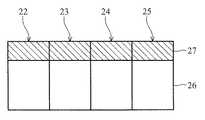
図2Bを参照すると、もう1つの従来のフルカラーOLEDディスプレイの画素構造が概略的に表されている。このフルカラーのOLEDディスプレイでは、各画素は、赤色サブピクセル域22、緑色サブピクセル域23、青色サブピクセル域24と、白色サブピクセル域25を含む。白色サブピクセル域25では、発光域26は、W−OLEDを有し、非発光域27は、W−OLEDの制御回路を有する。 Referring to FIG. 2B, the pixel structure of another conventional full color OLED display is schematically represented. In this full color OLED display, each pixel includes a
図2Aでは、白色画像を表示したい場合、赤色、緑色、青色サブピクセル域17、18と、19が組み合わされなければならない。しかし、図2Bでは、白色画像を表示したい場合、白色サブピクセル域25のみが発光を求められ、赤色、緑色、青色サブピクセル域22、23と、24は、発光をする必要がない。よって、白色画像が表示されている時、図2BのRGBW OLEDディスプレイは、通常、図2AのRGB OLEDディスプレイより少ない消費電力が求められる。しかし、非発光域の制御回路が固定された面積でなければならないことから、図2BのRGBW OLEDディスプレイは、より小さい発光域を有することになり、即ち、図2AのRGB OLEDディスプレイの開口率より低い開口率を有する。 In FIG. 2A, if a white image is to be displayed, the red, green and
発光システムを提供する。 Provide a light emitting system.
発光システムの実施例は、OLEDの画素構造を含む。画素構造は、第1OLEDを含む第1サブピクセル域と、第2OLEDと第1と第2OLEDを制御する電子部品を含む第2制御回路を含む第2サブピクセル域を含む。 An example of a light emitting system includes an OLED pixel structure. The pixel structure includes a first sub-pixel region including a first OLED and a second sub-pixel region including a second control circuit including electronic components that control the second OLED and the first and second OLEDs.
発光システムのもう1つの実施例では、OLEDの画素構造は、青色OLEDを含む青色サブピクセル域と、白色OLEDを含む白色サブピクセル域と、第2制御回路を含む。第2制御回路は、青色と白色OLEDを制御する電子部品を含む。青色サブピクセル域は、電子部品を含まないことができる。 In another embodiment of the light emitting system, the pixel structure of the OLED includes a blue subpixel region including a blue OLED, a white subpixel region including a white OLED, and a second control circuit. The second control circuit includes electronic components that control the blue and white OLEDs. The blue subpixel area may not include electronic components.
本発明の実施例では、B−OLEDを制御する電子部品をWサブピクセル域に配置することで、低い発光効率を有するB−OLEDの面積が増加され、よって、Bサブピクセル域のB−OLEDの全発光効率が向上されることができる。 In an embodiment of the present invention, the electronic component for controlling the B-OLED is disposed in the W sub-pixel region, thereby increasing the area of the B-OLED having a low luminous efficiency, and thus the B-OLED in the B sub-pixel region. The total luminous efficiency can be improved.
本発明についての目的、特徴、長所が一層明確に理解されるよう、以下に実施形態を例示し、図面を参照にしながら、詳細に説明する。 In order that the objects, features, and advantages of the present invention will be more clearly understood, embodiments will be described below in detail with reference to the drawings.
図3を参照すると、OLEDディスプレイの画素構造の実施例1が概略的に表されている。OLEDディスプレイの画素構造3は、第1サブピクセル域31と、第2サブピクセル域32を含む。第1サブピクセル域31は、第1OLED33を含むが制御回路を含まない。第2サブピクセル域32は、第2OLED34と制御回路35を含む。制御回路35は、第1制御回路部35aと、第2制御回路部35bを含む。第1制御回路部35aは、第1OLED33を制御する電子部品を含み、第2制御回路部35bは、第2OLED34を制御する電子部品を含む。 Referring to FIG. 3, Example 1 of the pixel structure of the OLED display is schematically represented. The
この実施例では、第1OLED33の発光効率は、第2OLED34の発光効率より低いことができる。例えば、第1OLED33は、青色OLEDであることができ、第2OLED34は、赤色、緑色、または白色OLEDであることができる。第1OLED33を制御する第1制御回路部35aが第1サブピクセル域31でなく、第2サブピクセル域32に配置されることから、第1OLED33の面積は、従来技術で用いられたのに比べ、増加されることができる。これは、第1サブピクセル域31の第1OLED33の輝度と寿命を増加することができる。 In this embodiment, the luminous efficiency of the
図4を参照すると、OLEDディスプレイの画素3の制御回路35の実施例1を概略的に表している。上述のように、制御回路部35aと35bの両方は、第2サブピクセル域32に配置される。第1制御回路部35aは、第1スイッチトランジスタ41、第1コンデンサ43と、第1OLED33を制御するように用いられる第1駆動トランジスタ45を含む。第2制御回路部35bは、第2スイッチトランジスタ42、第2コンデンサ44と、第2OLED34を制御するように用いられる第2駆動トランジスタ46を含む。 Referring to FIG. 4, a first embodiment of the
スキャンライン上の信号Vscan1が第1スイッチトランジスタ41のゲートに伝送された時、データライン上の信号Vdata1は、第1スイッチトランジスタ41によって第1コンデンサ43に伝送されて保存され、第1駆動トランジスタ45をオンにする。第1駆動トランジスタ45は、電圧レベルVdd1を有する電力線と第1OLED33を有し、よって、駆動回路を第1OLED33に提供する。第1OLED33は、電圧レベルVss1にも接続され、駆動電流を受ける。第1OLED33が駆動電流を受けた時、電力線より提供された電気エネルギーは、光エネルギーに変換される。上述のトランジスタでは、アモルファスシリコン(a−Si)薄膜トランジスタ(TFTs)、高温ポリシリコンTFTs、低温ポリシリコンTFTsと、単結晶シリコンTFTsを用いることができる。第1スイッチトランジスタ41、第1コンデンサ43及び第1駆動トランジスタ45が第2サブピクセル域32に配置されることで、従来技術に比べ、第1OLED33の面積を増加することができる。 When the signal Vscan1 on the scan line is transmitted to the gate of the
図5を参照すると、OLEDディスプレイの画素構造の実施例2が概略的に表されている。OLEDディスプレイの画素構造5は、第1サブピクセル域51と、第2サブピクセル域52を含む。第1サブピクセル域51は、第1OLED53と、第1OLED53を制御する電子部品を有する第1制御回路55を含む。第2サブピクセル域52は、第2OLED54と第2制御回路56を含む。第2制御回路56は、第1OLED53を制御する少なくとも1つの電子部品と、第2OLED54を制御する少なくとも1つの電子部品を含む。例えば、第2サブピクセル域52に配置された第2制御回路56は、第1OLED53を制御する第1制御回路部56aと、第2OLED54を制御する第2制御回路部56bを含む。この実施例では、第1OLED53の発光効率は、第2OLED54の発光効率より低いことができる。例えば、第1OLED53は、青色OLEDであることができ、第2OLED54は、赤色、緑色、または白色OLEDであることができる。第1OLED53を制御する少なくとも1つの電子部品は、第2サブピクセル域52に配置される。よって、第1OLED53の面積は、従来のOLEDに比べ、増加されることができる。よって、第1OLED53の輝度と寿命は、改善されることができる。 Referring to FIG. 5, Example 2 of the pixel structure of the OLED display is schematically represented. The
図6を参照すると、OLEDディスプレイの画素5の制御回路が概略的に表されている。第1制御回路55は、第1スイッチトランジスタ61を含む。第2制御回路56は、第1コンデンサ63と、第1駆動トランジスタ65を含む第1制御回路部56aと、第2スイッチトランジスタ62、第2コンデンサ64と、第2駆動トランジスタ66を含む第2制御回路部56bを含む。第1制御回路55と第1制御回路部56aは、第1OLED53を制御するように用いられる。第2制御回路部56bは、第2OLED54を制御するように用いられる。 Referring to FIG. 6, the control circuit of the
図7を参照すると、OLEDディスプレイの画素構造の実施例3が表されている。OLEDディスプレイの画素構造7は、Rサブピクセル域71と、Gサブピクセル域72、Bサブピクセル域73と、Wサブピクセル域74を含む。Rサブピクセル域71は、R−OLED711と、制御回路712を含む。Gサブピクセル域72は、G−OLED721と、制御回路722を含む。Bサブピクセル域73は、B−OLED731と、制御回路732を含む。Wサブピクセル域74は、W−OLED741と、制御回路742を含む。 Referring to FIG. 7, Example 3 of the pixel structure of the OLED display is shown. The
この実施例に基づいて、制御回路712は、スイッチトランジスタ、駆動トランジスタと、コンデンサを含む全電子部品を含み、R−OLED711を制御する。制御回路722は、スイッチトランジスタ、駆動トランジスタと、コンデンサを含む全電子部品を含み、G−OLED721を制御する。しかし、制御回路732は、一部の電子部品のみを含んでB−OLED731を制御する。B−OLED731を制御するその他の電子部品は、Wサブピクセル域74に配置される。例えば、図7に示すように、B−OLED731を制御する1つのトランジスタのみがBサブピクセル域73に配置され、B−OLED731を制御するトランジスタとコンデンサは、Wサブピクセル域74に配置される。よって、Wサブピクセル域74は、B−OLED731とW−OLED741の両方を制御する制御回路742を含む。 Based on this embodiment, the
よって、4色のサブピクセル域の中で、Bサブピクセル域73に配置された制御回路732は、面積が最も小さく、Wサブピクセル域74に配置された制御回路742は、面積が最も大きい。一般的に、4色のOLED材料の中で、白色OLEDが最も高い発光効率を有し、青色が最も低い発光効率を有する。よって、B−OLEDを制御する電子部品を再配置(e.g.B−OLEDを制御する電子部品を白色サブピクセル域に配置)することで、B−OLEDの面積が増加され、W−OLEDの面積が減少される。よって、Bサブピクセル域のB−OLEDの全発光効率と、Wサブピクセル域のW−OLEDの全発光効率が最適に調整されることができる。 Therefore, the
図8は、ディスプレイ装置80として実施されるシステムの実施例を表している。ディスプレイ装置80は、図7に示す画素構造7のような画素構造を組み込んだディスプレイパネル81を含む。ディスプレイパネル81は、コントローラ82に接続することができる。コントローラ82は、ソースとゲート駆動回路(未表示)を含むことができ、ディスプレイパネル81を制御してディスプレイ装置80を操作する。 FIG. 8 illustrates an example of a system implemented as the
図9は、電子装置90として実施されるシステムの実施例を表している概略図である。電子装置90は、図8に示すディスプレイ装置80のようなディスプレイ装置を組み込む。入力装置91は、ディスプレイ装置80のコントローラ82に接続される。入力装置91は、画像データをコントローラ82に入力して画像を表示するプロセッサ、または同種のものを含むことができる。電子装置90は、PDA、ノート型パソコン、携帯用コンピュータ、携帯電話、またはディスプレイモニタ装置、または例えばデスクトップ型コンピュータなどの携帯できない装置であることができる。 FIG. 9 is a schematic diagram illustrating an example of a system implemented as the electronic device 90. Electronic device 90 incorporates a display device, such as
以上、本発明の好適な実施例を例示したが、これは本発明を限定するものではなく、本発明の精神及び範囲を逸脱しない限りにおいては、当業者であれば行い得る少々の変更や修飾を付加することは可能である。従って、本発明が保護を請求する範囲は、特許請求の範囲を基準とする。 The preferred embodiments of the present invention have been described above, but this does not limit the present invention, and a few changes and modifications that can be made by those skilled in the art without departing from the spirit and scope of the present invention. It is possible to add. Accordingly, the scope of the protection claimed by the present invention is based on the scope of the claims.
3 画素
5、7画素構造
11 サブピクセル
12 電力線
13 データライン
14 スキャンライン
15、20、26 発光域
16、21、27 非発光域
17、22、71 赤色サブピクセル
18、23、72 緑色サブピクセル
19、24、73 青色サブピクセル
25、74 白色サブピクセル
31 第1サブピクセル
32 第2サブピクセル
33、53 第1OLED
34、54 第1OLED
35 制御回路
35a 第1制御回路部
35b 第2制御回路部
41、61 第1スイッチトランジスタ
42、62 第2スイッチトランジスタ
43、63 第1コンデンサ
44、64 第2コンデンサ
45、65 第1駆動トランジスタ
46、66 第2駆動トランジスタ
51 第1サブピクセル域
52 第2サブピクセル域
55 第1制御回路
56 第2制御回路
56a 第1制御回路部
56b 第2制御回路部
80 ディスプレイ装置
81 ディスプレイパネル
82 コントローラ
90 電子装置
91 入力装置
711 赤色OLED
712、722、732、742 制御回路
721 緑色OLED
731 青色OLED
741 白色OLED
Vscan1、Vscan2、Vdata1、Vdata2 信号
Vdd1、Vdd2、Vss1、Vss2 電源
3
34, 54 1st OLED
35
712, 722, 732, 742
731 Blue OLED
741 White OLED
Vscan1, Vscan2, Vdata1, Vdata2 Signals Vdd1, Vdd2, Vss1, Vss2 Power supply
Claims (19)
Translated fromJapanese前記画素構造は、
第1の有機発光ダイオード(第1OLED)を含む第1サブピクセル域、および
第2の有機発光ダイオード(第2OLED)と、前記第1の有機発光ダイオード(第1OLED)と前記第2の有機発光ダイオード(第2OLED)を制御する電子部品を含む第2制御回路を含む第2サブピクセル域
を含む発光システム。A light emitting system including a pixel structure of an organic light emitting diode (OLED),
The pixel structure is
A first sub-pixel region including a first organic light emitting diode (first OLED); a second organic light emitting diode (second OLED); the first organic light emitting diode (first OLED); and the second organic light emitting diode. A light emitting system including a second sub-pixel region including a second control circuit including an electronic component for controlling the (second OLED).
第1の有機発光ダイオード(第1OLED)を含む第1サブピクセル域、
第2の有機発光ダイオード(第2OLED)と第2制御回路を含み、前記第2制御回路は、前記第2の有機発光ダイオード(第2OLED)を制御する電子部品と、前記第1の有機発光ダイオード(第1OLED)、第3の有機発光ダイオード(第3OLED)、第4の有機発光ダイオード(第4OLED)の任意の1つ、または前記第1、第3と第4の有機発光ダイオード(第1、第3及び第4OLED)の組み合わせを制御する電子部品を含む第2サブピクセル域、
第3の有機発光ダイオード(第3OLED)を含む第3サブピクセル域、および
第4の有機発光ダイオード(第4OLED)を含む第4サブピクセル域を含む発光システム。A light emitting system including a device having an OLED pixel structure,
A first sub-pixel region comprising a first organic light emitting diode (first OLED);
A second organic light emitting diode (second OLED); and a second control circuit, wherein the second control circuit controls the second organic light emitting diode (second OLED) and the first organic light emitting diode. (First OLED), any one of a third organic light emitting diode (third OLED), a fourth organic light emitting diode (fourth OLED), or the first, third and fourth organic light emitting diodes (first, A second sub-pixel area comprising electronic components that control the combination of the third and fourth OLEDs);
A light emitting system including a third subpixel region including a third organic light emitting diode (third OLED) and a fourth subpixel region including a fourth organic light emitting diode (fourth OLED).
第1の有機発光ダイオード(第1OLED)と前記第1の有機発光ダイオード(第1OLED)を制御する第1制御回路を含む第1サブピクセル域、
第2の有機発光ダイオード(第2OLED)と第2制御回路を含み、前記第2制御回路は、前記第2の有機発光ダイオード(第2OLED)を制御する電子部品と、前記第1の有機発光ダイオード(第1OLED)、第3の有機発光ダイオード(第3OLED)、第4の有機発光ダイオード(第4OLED)の任意の1つ、または前記第1、第3と第4の有機発光ダイオード(第1、第3及び第4OLED)の組み合わせを制御する電子部品を含む第2サブピクセル域、
第3の有機発光ダイオード(第3OLED)と前記第3の有機発光ダイオード(第3OLED)を制御する第3制御回路を含む第3サブピクセル域、および
第4の有機発光ダイオード(第4OLED)と前記第4の有機発光ダイオード(第4OLED)を制御する第4制御回路を含む第4サブピクセル域を含む請求項3に記載のシステム。A light emitting system including a device having an OLED pixel structure,
A first sub-pixel region including a first organic light emitting diode (first OLED) and a first control circuit for controlling the first organic light emitting diode (first OLED);
A second organic light emitting diode (second OLED); and a second control circuit, wherein the second control circuit controls the second organic light emitting diode (second OLED) and the first organic light emitting diode. (First OLED), any one of a third organic light emitting diode (third OLED), a fourth organic light emitting diode (fourth OLED), or the first, third and fourth organic light emitting diodes (first, A second sub-pixel area comprising electronic components that control the combination of the third and fourth OLEDs);
A third sub-pixel region including a third organic light emitting diode (third OLED) and a third control circuit for controlling the third organic light emitting diode (third OLED); and a fourth organic light emitting diode (fourth OLED) and the 4. The system according to claim 3, comprising a fourth sub-pixel area comprising a fourth control circuit for controlling a fourth organic light emitting diode (fourth OLED).
前記画素構造は前記ディスプレイ装置の一部を形成する請求項1に記載のシステム。The system further includes a display device; and
The system of claim 1, wherein the pixel structure forms part of the display device.
The system of claim 16, further comprising a device for displaying an image displayed by the display device.
Applications Claiming Priority (1)
| Application Number | Priority Date | Filing Date | Title |
|---|---|---|---|
| US11/230,432US20070063192A1 (en) | 2005-09-20 | 2005-09-20 | Systems for emitting light incorporating pixel structures of organic light-emitting diodes |
Publications (1)
| Publication Number | Publication Date |
|---|---|
| JP2007149640Atrue JP2007149640A (en) | 2007-06-14 |
Family
ID=37883176
Family Applications (1)
| Application Number | Title | Priority Date | Filing Date |
|---|---|---|---|
| JP2006213001APendingJP2007149640A (en) | 2005-09-20 | 2006-08-04 | Emission system incorporating pixel structure of organic light emitting diode |
Country Status (4)
| Country | Link |
|---|---|
| US (1) | US20070063192A1 (en) |
| JP (1) | JP2007149640A (en) |
| CN (1) | CN100474989C (en) |
| TW (1) | TW200713168A (en) |
Cited By (5)
| Publication number | Priority date | Publication date | Assignee | Title |
|---|---|---|---|---|
| KR20100069337A (en)* | 2008-12-16 | 2010-06-24 | 엘지디스플레이 주식회사 | Top emission white organic light emitting display device |
| JP2013250555A (en)* | 2012-05-31 | 2013-12-12 | Samsung Display Co Ltd | Display panel |
| JP2015161945A (en)* | 2014-02-25 | 2015-09-07 | 三星ディスプレイ株式會社Samsung Display Co.,Ltd. | Display device |
| JP2016090595A (en)* | 2014-10-29 | 2016-05-23 | 株式会社ジャパンディスプレイ | Display device |
| WO2023106049A1 (en)* | 2021-12-10 | 2023-06-15 | ソニーグループ株式会社 | Display device and electronic apparatus |
Families Citing this family (13)
| Publication number | Priority date | Publication date | Assignee | Title |
|---|---|---|---|---|
| US7700471B2 (en)* | 2005-12-13 | 2010-04-20 | Versatilis | Methods of making semiconductor-based electronic devices on a wire and articles that can be made thereby |
| US7638416B2 (en)* | 2005-12-13 | 2009-12-29 | Versatilis Llc | Methods of making semiconductor-based electronic devices on a wire and articles that can be made using such devices |
| TWI275052B (en)* | 2006-04-07 | 2007-03-01 | Ind Tech Res Inst | OLED pixel structure and method of manufacturing the same |
| US7499116B2 (en)* | 2006-04-11 | 2009-03-03 | Tpo Displays Corp. | Systems for displaying images having micro-reflective transmission liquid crystal display with particular storage capacitor arrangement |
| JP4807366B2 (en)* | 2008-03-11 | 2011-11-02 | ソニー株式会社 | Display device |
| KR101113345B1 (en)* | 2010-03-24 | 2012-02-29 | 삼성모바일디스플레이주식회사 | Plate panel display device and making method for the same |
| GB2495107A (en)* | 2011-09-28 | 2013-04-03 | Cambridge Display Tech Ltd | Organic light emitting diode display device with further small-area sacrificial diodes |
| GB2495117A (en)* | 2011-09-29 | 2013-04-03 | Cambridge Display Tech Ltd | Display driver circuits for OLED displays |
| TWI518657B (en)* | 2014-03-31 | 2016-01-21 | 友達光電股份有限公司 | Pixel unit of organic electroluminescent display |
| KR20160087022A (en)* | 2015-01-12 | 2016-07-21 | 삼성디스플레이 주식회사 | Display panel |
| KR102636147B1 (en)* | 2015-12-31 | 2024-02-08 | 엘지디스플레이 주식회사 | Transparent display device |
| WO2018120314A1 (en)* | 2016-12-27 | 2018-07-05 | 武汉华星光电技术有限公司 | Display panel and array substrate thereof |
| KR102741338B1 (en)* | 2020-07-07 | 2024-12-13 | 삼성디스플레이 주식회사 | Display device |
Citations (4)
| Publication number | Priority date | Publication date | Assignee | Title |
|---|---|---|---|---|
| JP2002244617A (en)* | 2001-02-15 | 2002-08-30 | Sanyo Electric Co Ltd | Organic el pixel circuit |
| JP2004184530A (en)* | 2002-11-29 | 2004-07-02 | Seiko Epson Corp | Electro-optical device, active matrix substrate and electronic equipment |
| JP2005129505A (en)* | 2003-09-30 | 2005-05-19 | Sanyo Electric Co Ltd | Luminescent display device and its pixel layout formation method |
| JP2006244892A (en)* | 2005-03-04 | 2006-09-14 | Chunghwa Picture Tubes Ltd | Active-matrix organic el device array |
Family Cites Families (20)
| Publication number | Priority date | Publication date | Assignee | Title |
|---|---|---|---|---|
| US5773130A (en)* | 1996-06-06 | 1998-06-30 | Motorola, Inc. | Multi-color organic electroluminescent device |
| TW587239B (en)* | 1999-11-30 | 2004-05-11 | Semiconductor Energy Lab | Electric device |
| JP3989718B2 (en)* | 2001-01-18 | 2007-10-10 | シャープ株式会社 | Memory integrated display element |
| US6693385B2 (en)* | 2001-03-22 | 2004-02-17 | Semiconductor Energy Laboratory Co., Ltd. | Method of driving a display device |
| US7317205B2 (en)* | 2001-09-10 | 2008-01-08 | Semiconductor Energy Laboratory Co., Ltd. | Light emitting device and method of manufacturing a semiconductor device |
| US6872472B2 (en)* | 2002-02-15 | 2005-03-29 | Eastman Kodak Company | Providing an organic electroluminescent device having stacked electroluminescent units |
| KR100902244B1 (en)* | 2002-12-31 | 2009-06-11 | 엘지디스플레이 주식회사 | Thin film transistor type liquid crystal display device |
| EP1471494A1 (en)* | 2003-04-24 | 2004-10-27 | Barco N.V. | Organic light-emitting diode drive circuit for a display application |
| US6771028B1 (en)* | 2003-04-30 | 2004-08-03 | Eastman Kodak Company | Drive circuitry for four-color organic light-emitting device |
| US7030553B2 (en)* | 2003-08-19 | 2006-04-18 | Eastman Kodak Company | OLED device having microcavity gamut subpixels and a within gamut subpixel |
| TWI263184B (en)* | 2003-09-30 | 2006-10-01 | Sanyo Electric Co | Electroluminescence display device |
| US8144100B2 (en)* | 2003-12-17 | 2012-03-27 | Samsung Electronics Co., Ltd. | Shared buffer display panel drive methods and systems |
| KR101066411B1 (en)* | 2004-03-31 | 2011-09-21 | 삼성전자주식회사 | Display device and manufacturing method thereof |
| JP4143569B2 (en)* | 2004-05-14 | 2008-09-03 | キヤノン株式会社 | Color display device |
| KR100600350B1 (en)* | 2004-05-15 | 2006-07-14 | 삼성에스디아이 주식회사 | Demultiplexing and organic electroluminescent display device having same |
| JP4737587B2 (en)* | 2004-06-18 | 2011-08-03 | 奇美電子股▲ふん▼有限公司 | Driving method of display device |
| US20060001914A1 (en)* | 2004-06-30 | 2006-01-05 | Mesmer Ralph M | Color scanner display |
| CN1774147A (en)* | 2004-11-08 | 2006-05-17 | 中华映管股份有限公司 | Active OLED Array |
| US7646367B2 (en)* | 2005-01-21 | 2010-01-12 | Semiconductor Energy Laboratory Co., Ltd. | Semiconductor device, display device and electronic apparatus |
| TWI339835B (en)* | 2005-02-03 | 2011-04-01 | Chimei Innolux Corp | Pixel structure for a color display device, organic light emitting device module, electronic device and method of rendering color of a pixel in a display device |
- 2005
- 2005-09-20USUS11/230,432patent/US20070063192A1/ennot_activeAbandoned
- 2006
- 2006-05-16TWTW095117246Apatent/TW200713168A/enunknown
- 2006-08-04JPJP2006213001Apatent/JP2007149640A/enactivePending
- 2006-08-25CNCNB2006101117427Apatent/CN100474989C/enactiveActive
Patent Citations (4)
| Publication number | Priority date | Publication date | Assignee | Title |
|---|---|---|---|---|
| JP2002244617A (en)* | 2001-02-15 | 2002-08-30 | Sanyo Electric Co Ltd | Organic el pixel circuit |
| JP2004184530A (en)* | 2002-11-29 | 2004-07-02 | Seiko Epson Corp | Electro-optical device, active matrix substrate and electronic equipment |
| JP2005129505A (en)* | 2003-09-30 | 2005-05-19 | Sanyo Electric Co Ltd | Luminescent display device and its pixel layout formation method |
| JP2006244892A (en)* | 2005-03-04 | 2006-09-14 | Chunghwa Picture Tubes Ltd | Active-matrix organic el device array |
Cited By (12)
| Publication number | Priority date | Publication date | Assignee | Title |
|---|---|---|---|---|
| KR20100069337A (en)* | 2008-12-16 | 2010-06-24 | 엘지디스플레이 주식회사 | Top emission white organic light emitting display device |
| KR101649224B1 (en)* | 2008-12-16 | 2016-08-18 | 엘지디스플레이 주식회사 | Top Emission White Organic Light Emitting Display Device |
| JP2013250555A (en)* | 2012-05-31 | 2013-12-12 | Samsung Display Co Ltd | Display panel |
| US20160307517A1 (en) | 2012-05-31 | 2016-10-20 | Samsung Display Co., Ltd. | Display panel |
| JP2018106184A (en)* | 2012-05-31 | 2018-07-05 | 三星ディスプレイ株式會社Samsung Display Co.,Ltd. | Display panel |
| JP2019174810A (en)* | 2012-05-31 | 2019-10-10 | 三星ディスプレイ株式會社Samsung Display Co.,Ltd. | Display panel |
| US10783833B2 (en) | 2012-05-31 | 2020-09-22 | Samsung Display Co., Ltd. | Display panel |
| US11282464B2 (en) | 2012-05-31 | 2022-03-22 | Samsung Display Co., Ltd. | Display panel |
| JP2015161945A (en)* | 2014-02-25 | 2015-09-07 | 三星ディスプレイ株式會社Samsung Display Co.,Ltd. | Display device |
| JP2016090595A (en)* | 2014-10-29 | 2016-05-23 | 株式会社ジャパンディスプレイ | Display device |
| WO2023106049A1 (en)* | 2021-12-10 | 2023-06-15 | ソニーグループ株式会社 | Display device and electronic apparatus |
| US12417732B2 (en) | 2021-12-10 | 2025-09-16 | Sony Group Corporation | Display apparatus and electronic equipment |
Also Published As
| Publication number | Publication date |
|---|---|
| CN100474989C (en) | 2009-04-01 |
| CN1937869A (en) | 2007-03-28 |
| US20070063192A1 (en) | 2007-03-22 |
| TW200713168A (en) | 2007-04-01 |
Similar Documents
| Publication | Publication Date | Title |
|---|---|---|
| JP2007149640A (en) | Emission system incorporating pixel structure of organic light emitting diode | |
| JP4295768B2 (en) | Organic light emitting display device and method for displaying image thereof | |
| US8031140B2 (en) | Display device and driving method thereof | |
| TWI389077B (en) | Organic light emitting diode display device and driving method thereof | |
| US8605127B2 (en) | Method for driving active matrix organic light emitting diode display panel | |
| US9305487B2 (en) | Organic light emitting diode display and method for driving display panel thereof | |
| TWI433110B (en) | Electroluminescent display and method of driving same | |
| JP2010170070A (en) | Organic electroluminescent display device, and method of driving the same | |
| JP2003168561A (en) | Self-luminous display | |
| KR20190069666A (en) | Display device and driving method of the same | |
| TWI881562B (en) | Display panel and display apparatus | |
| JP4999390B2 (en) | Display device | |
| CN107886899A (en) | Organic electroluminescence display panel and the organic light-emitting display device for including it | |
| US10475384B2 (en) | Display device comprising a lighting part | |
| US20080117196A1 (en) | Display device and driving method thereof | |
| JP2002287664A (en) | Display panel and its driving method | |
| US7916112B2 (en) | Systems for controlling pixels | |
| JP2005235566A (en) | Electro-optical device and electronic apparatus | |
| WO2023178520A1 (en) | Light emitting substrate, display panel, display apparatus, and display method | |
| US20250182680A1 (en) | Display Apparatus | |
| US20250218347A1 (en) | Pixel circuit | |
| KR20250133546A (en) | Display apparatus | |
| KR20250132316A (en) | Display module and display apparatus having the same | |
| KR20250148324A (en) | Display module and display apparatus having the same | |
| KR20250132869A (en) | Display apparatus |
Legal Events
| Date | Code | Title | Description |
|---|---|---|---|
| A131 | Notification of reasons for refusal | Free format text:JAPANESE INTERMEDIATE CODE: A131 Effective date:20091110 | |
| A521 | Request for written amendment filed | Free format text:JAPANESE INTERMEDIATE CODE: A523 Effective date:20100208 | |
| A131 | Notification of reasons for refusal | Free format text:JAPANESE INTERMEDIATE CODE: A131 Effective date:20100302 | |
| A601 | Written request for extension of time | Free format text:JAPANESE INTERMEDIATE CODE: A601 Effective date:20100602 | |
| A602 | Written permission of extension of time | Free format text:JAPANESE INTERMEDIATE CODE: A602 Effective date:20100607 | |
| A02 | Decision of refusal | Free format text:JAPANESE INTERMEDIATE CODE: A02 Effective date:20100907 |