JP2007133026A - Method of manufacturing optical waveguide with v-groove - Google Patents
Method of manufacturing optical waveguide with v-grooveDownload PDFInfo
- Publication number
- JP2007133026A JP2007133026AJP2005323937AJP2005323937AJP2007133026AJP 2007133026 AJP2007133026 AJP 2007133026AJP 2005323937 AJP2005323937 AJP 2005323937AJP 2005323937 AJP2005323937 AJP 2005323937AJP 2007133026 AJP2007133026 AJP 2007133026A
- Authority
- JP
- Japan
- Prior art keywords
- resin
- optical waveguide
- groove
- layer
- fluorinated
- Prior art date
- Legal status (The legal status is an assumption and is not a legal conclusion. Google has not performed a legal analysis and makes no representation as to the accuracy of the status listed.)
- Pending
Links
- 230000003287optical effectEffects0.000titleclaimsabstractdescription74
- 238000004519manufacturing processMethods0.000titleclaimsabstractdescription27
- 239000011347resinSubstances0.000claimsabstractdescription64
- 229920005989resinPolymers0.000claimsabstractdescription64
- 239000000758substrateSubstances0.000claimsabstractdescription43
- 239000000463materialSubstances0.000claimsabstractdescription39
- XUIMIQQOPSSXEZ-UHFFFAOYSA-NSiliconChemical compound[Si]XUIMIQQOPSSXEZ-UHFFFAOYSA-N0.000claimsabstractdescription27
- 239000010703siliconSubstances0.000claimsabstractdescription27
- 229910052710siliconInorganic materials0.000claimsabstractdescription27
- 229920001721polyimidePolymers0.000claimsabstractdescription21
- 238000000034methodMethods0.000claimsabstractdescription17
- 239000009719polyimide resinSubstances0.000claimsabstractdescription9
- 239000013307optical fiberSubstances0.000claimsabstractdescription8
- -1polysiloxanePolymers0.000claimsabstractdescription5
- 239000004925Acrylic resinSubstances0.000claimsabstractdescription4
- 229920000178Acrylic resinPolymers0.000claimsabstractdescription4
- NIXOWILDQLNWCW-UHFFFAOYSA-Nacrylic acid groupChemical groupC(C=C)(=O)ONIXOWILDQLNWCW-UHFFFAOYSA-N0.000claimsabstractdescription4
- 125000002723alicyclic groupChemical group0.000claimsabstractdescription4
- 239000003822epoxy resinSubstances0.000claimsabstractdescription4
- 229920000647polyepoxidePolymers0.000claimsabstractdescription4
- 229920001296polysiloxanePolymers0.000claimsabstractdescription4
- 150000003376siliconChemical class0.000claimsabstractdescription3
- 229920000642polymerPolymers0.000abstractdescription10
- 239000012790adhesive layerSubstances0.000abstractdescription3
- 239000010410layerSubstances0.000description65
- YCKRFDGAMUMZLT-UHFFFAOYSA-NFluorine atomChemical compound[F]YCKRFDGAMUMZLT-UHFFFAOYSA-N0.000description12
- 239000004642PolyimideSubstances0.000description12
- 229910052731fluorineInorganic materials0.000description12
- 239000011737fluorineSubstances0.000description12
- VYPSYNLAJGMNEJ-UHFFFAOYSA-NSilicium dioxideChemical compoundO=[Si]=OVYPSYNLAJGMNEJ-UHFFFAOYSA-N0.000description10
- 239000012792core layerSubstances0.000description8
- 238000005253claddingMethods0.000description7
- 238000001020plasma etchingMethods0.000description7
- 239000002699waste materialSubstances0.000description7
- 238000001039wet etchingMethods0.000description7
- KRHYYFGTRYWZRS-UHFFFAOYSA-NFluoraneChemical compoundFKRHYYFGTRYWZRS-UHFFFAOYSA-N0.000description6
- 150000001875compoundsChemical class0.000description6
- 238000011161developmentMethods0.000description6
- 238000000206photolithographyMethods0.000description6
- 235000012239silicon dioxideNutrition0.000description5
- 239000000377silicon dioxideSubstances0.000description5
- 150000002902organometallic compoundsChemical class0.000description4
- 230000005540biological transmissionEffects0.000description3
- 238000004891communicationMethods0.000description3
- 238000004528spin coatingMethods0.000description3
- 230000015572biosynthetic processEffects0.000description2
- 238000005516engineering processMethods0.000description2
- 238000005530etchingMethods0.000description2
- 238000001755magnetron sputter depositionMethods0.000description2
- 229920005575poly(amic acid)Polymers0.000description2
- 238000012545processingMethods0.000description2
- 239000002966varnishSubstances0.000description2
- 230000000052comparative effectEffects0.000description1
- 238000007796conventional methodMethods0.000description1
- 238000013036cure processMethods0.000description1
- 238000005520cutting processMethods0.000description1
- 238000000354decomposition reactionMethods0.000description1
- 230000002950deficientEffects0.000description1
- 238000010586diagramMethods0.000description1
- 238000001312dry etchingMethods0.000description1
- 238000010304firingMethods0.000description1
- 238000010438heat treatmentMethods0.000description1
- 238000000059patterningMethods0.000description1
Images

Landscapes
- Optical Integrated Circuits (AREA)
- Optical Couplings Of Light Guides (AREA)
Abstract
Description
Translated fromJapanese本発明は、V溝付き光導波路の製造方法に関する。 The present invention relates to a method for manufacturing a V-grooved optical waveguide.
情報通信システムの基盤技術として光通信技術が浸透していくにつれて光導波路は、光ネットワーク用キーデバイスとして益々その重要性が高まると同時に、電子回路配線基板等の分野への応用に向けて開発が進められている。また、インターネットの普及により、情報伝送量が増大し、その伝送速度の高速化が望まれている。 As optical communication technology has permeated as a basic technology for information communication systems, optical waveguides are becoming increasingly important as key devices for optical networks, and at the same time, they are being developed for applications in fields such as electronic circuit wiring boards. It is being advanced. Further, with the spread of the Internet, the amount of information transmission increases, and it is desired to increase the transmission speed.
光導波路の応用として、光導波路、光導波路に光を入射する光ファイバ、あるいは光導波路から出射した光を受光する光ファイバを固定するためのV溝を同一基板上に備えたデバイスの高性能化、安価な製造方法の開発が切望されている。 As an application of an optical waveguide, high performance of a device having a V-groove on the same substrate for fixing an optical waveguide, an optical fiber that enters light into the optical waveguide, or an optical fiber that receives light emitted from the optical waveguide. Therefore, development of an inexpensive manufacturing method is eagerly desired.
また、光導波路デバイスの普及には低価格化と量産化が要望されており、樹脂製光導波路がその有力な候補として開発されている。 導波路用の樹脂材料としては、フッ素化ポリイミド樹脂、フッ素化アクリル樹脂、重水素化ポリシロキサン樹脂、フッ素化エポキシ樹脂、全フッ素化脂環式樹脂、シリコン樹脂等が用いられ、近赤外の光通信波長帯域である1.3〜1.5ミクロン帯での透明性を確保するために、C−H結合をC−D結合やC−F結合に置換した樹脂材料が用いられている。なかでも、フッ素化ポリイミド樹脂は近赤外領域での透過特性がすぐれており、そのうえ、最も耐熱性が高く、強度も確保できるところから、樹脂光導波路用の材料としては最も適している。 Further, the spread of optical waveguide devices is demanded to reduce the price and mass production, and resin optical waveguides have been developed as promising candidates. As the resin material for the waveguide, fluorinated polyimide resin, fluorinated acrylic resin, deuterated polysiloxane resin, fluorinated epoxy resin, perfluorinated alicyclic resin, silicon resin, etc. are used. In order to ensure transparency in the 1.3 to 1.5 micron band which is an optical communication wavelength band, a resin material in which a C—H bond is replaced with a C—D bond or a C—F bond is used. Among these, fluorinated polyimide resins are most suitable as materials for resin optical waveguides because of their excellent transmission characteristics in the near-infrared region and the highest heat resistance and sufficient strength.
このようなフッ素含有樹脂材料を用い、同一基板上に光導波路、V溝を有したデバイスの製造方法としては、例えば、基板上にV溝を形成し、樹脂材料と基板との密着性向上のための密着層、下部クラッド層、コア層を成膜し、フォトリソグラフィと反応性イオンエッチング(RIE、Reactive Ion Etching)の技法によりリッジ型コアパターンを形成し、さらに上部クラッドを形成して導波路を埋め込み、その後、V溝上に形成された導波路を除去する方法が考えられる。しかしこの方法では、V溝内にポリマー屑が残る可能性がある。 As a method of manufacturing a device having such an optical waveguide and V-groove on the same substrate using such a fluorine-containing resin material, for example, a V-groove is formed on the substrate to improve the adhesion between the resin material and the substrate. For this purpose, an adhesion layer, a lower cladding layer, and a core layer are formed, a ridge-type core pattern is formed by photolithography and reactive ion etching (RIE), and an upper cladding is formed to form a waveguide. Then, a method of removing the waveguide formed on the V-groove is conceivable. However, this method may leave polymer waste in the V-groove.
また、別の方法として、基板上にV溝を形成する工程、光導波路形成領域に密着層を形成する工程(この際、V溝領域に形成された密着層は下部クラッド形成前に除去しておく)、下部クラッド、コア層を形成する工程、コア上にレジスト層を形成し、レジスト層を光導波路形状にパターニングにしてコアを形成する工程、上部クラッドを形成する工程、V溝形成領域の下部クラッド、コア、上部クラッド層を除去する工程からなる方法が紹介されている(特許文献1参照)。
前述した例えば特開2003−315584号公報に記載の方法は、V溝領域に形成された密着層除去の方法として、基板全面に形成した密着層上にレジスト膜を形成し、フォトリソ工程、現像により、V溝領域のレジスト膜を除去するが、その際、V溝領域に形成されていた密着層、例えばフッ素を含有しないポリイミドを同時にウエットエッチングし、V溝領域の密着層を除去するものである。 For example, the method described in Japanese Patent Application Laid-Open No. 2003-315584 described above is a method for removing the adhesion layer formed in the V-groove region by forming a resist film on the adhesion layer formed on the entire surface of the substrate, and performing photolithography process and development. The resist film in the V-groove region is removed. At this time, the adhesion layer formed in the V-groove region, for example, polyimide not containing fluorine is simultaneously wet-etched to remove the adhesion layer in the V-groove region. .
しかしながら、V溝内の密着層除去具合が不十分であったり、ばらついたりし、ポリマー屑が残る場合があり、歩留まり低下の現象が見られる。これは、使用する密着層、例えばフッ素を含有しないポリイミドは膜形成にあたり、フルキュアを実施しているため、下地基板への密着性が高くなる、レジスト現像液への溶解性が低下していること等が原因と考えられる。 However, the degree of adhesion layer removal in the V-groove may be insufficient or may vary, and polymer waste may remain, resulting in a decrease in yield. This is because the adhesion layer to be used, for example, polyimide not containing fluorine, is subjected to full cure in forming the film, so that the adhesion to the base substrate is increased and the solubility in the resist developer is reduced. This is considered to be the cause.
また、一度形成した密着層を、レジストを使用して除去する工程があり、工程の簡易化も望まれている。 Further, there is a step of removing the adhesive layer once formed using a resist, and simplification of the step is also desired.
本発明は、光導波路、V溝を同一基板上に備えたデバイスの製造において、V溝領域にポリマー屑が残存せず、製造歩留まりを向上できる安易な製造方法を提供することを課題とする。 An object of the present invention is to provide an easy manufacturing method capable of improving the manufacturing yield without producing polymer waste in the V groove region in the manufacture of a device having an optical waveguide and a V groove on the same substrate.
なお、本発明において、V溝領域とは、V溝内およびデバイス作製後においてV溝周辺部の光導波路の必要ない部分のことを意味する。 In the present invention, the V-groove region means an unnecessary portion of the optical waveguide in the V-groove and in the periphery of the V-groove after device fabrication.
本発明は、同一基板上に、樹脂光導波路と光ファイバ固定用のV溝を有する光デバイスにおいて、樹脂光導波路と基板との間の密着層に感光性樹脂材料を使用することを特徴とする光デバイスの製造方法である。 The present invention is characterized in that, in an optical device having a resin optical waveguide and a V-groove for fixing an optical fiber on the same substrate, a photosensitive resin material is used for an adhesion layer between the resin optical waveguide and the substrate. It is a manufacturing method of an optical device.
また光導波路用樹脂材料がフッ素化ポリイミド樹脂、全フッ素化ポリイミド樹脂、フッ素化シリコン樹脂、フッ素化アクリル樹脂、重水素化ポリシロキサン樹脂、フッ素化エポキシ樹脂、全フッ素化脂環式樹脂、シリコン樹脂のいずれかであり、感光性樹脂材料が耐熱性感光性樹脂であることを特徴とする、上記の光デバイスの製造方法である。 Optical waveguide resin materials are fluorinated polyimide resin, perfluorinated polyimide resin, fluorinated silicon resin, fluorinated acrylic resin, deuterated polysiloxane resin, fluorinated epoxy resin, perfluorinated alicyclic resin, silicon resin. Any one of the above, wherein the photosensitive resin material is a heat-resistant photosensitive resin.
また、上記の製造方法により製造したV溝付き光導波路デバイスである。 Moreover, it is an optical waveguide device with a V groove manufactured by said manufacturing method.
本発明によれば、光導波路、V溝を同一基板上に備えたデバイスの製造において、V溝領域にポリマー屑が残存せず、製造歩留まりを向上できる安易な製造方法を提供できる。 ADVANTAGE OF THE INVENTION According to this invention, in manufacture of the device provided with the optical waveguide and V groove | channel on the same board | substrate, polymer waste does not remain in a V groove area | region, but the easy manufacturing method which can improve a manufacturing yield can be provided.
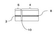
図1、2は本発明に係わるV溝付き光導波路を説明する図である。 1 and 2 are views for explaining a V-grooved optical waveguide according to the present invention.
基板には表面に二酸化珪素膜1を有するシリコン基板2が用いられる。二酸化珪素膜1をフォトリソグラフィとウエットエッチングあるいはドライエッチングにより加工し、その後、シリコンの異方性を利用し、ウエットエッチングによりV溝3を作製する。V溝3の幅および深さは、光ファイバを固定した際、形成する光導波路のコアと光軸高さが一致するよう設計しておく必要がある。 As the substrate, a
樹脂材料、特に光導波路材料として好適なフッ素を含有する樹脂材料は一般的にシリコンや二酸化珪素膜を有するシリコンなどとの密着性が悪い。このため、これら基板上に光導波路を作製する場合には、基板と光導波路材料との密着性向上のため、基板と光導波路下部クラッド層の間に、密着層を設けることが必要である。 Resin materials, particularly resin materials containing fluorine, which are suitable as optical waveguide materials, generally have poor adhesion to silicon or silicon having a silicon dioxide film. For this reason, when an optical waveguide is produced on these substrates, it is necessary to provide an adhesion layer between the substrate and the optical waveguide lower cladding layer in order to improve the adhesion between the substrate and the optical waveguide material.
密着層としては、フッ素を含有していない樹脂材料、例えばフッ素を含有しないポリイミドなどが高耐熱性の観点より好適である。また、シリコンを含有するポリイミドシリコンなどが挙げられる。さらには、有機アルミニウム化合物、有機チタン化合物、有機ジルコニウム化合物などの有機金属化合物も挙げられる。上記樹脂材料、有機金属化合物を単独で用いても良いし、併用しても構わない。また、基板と光導波路材料との密着性が得られればその方法に限定されるものではない。 As the adhesion layer, a resin material that does not contain fluorine, for example, polyimide that does not contain fluorine, is preferable from the viewpoint of high heat resistance. Moreover, the polyimide silicon containing silicon etc. are mentioned. Furthermore, organometallic compounds such as organoaluminum compounds, organotitanium compounds, and organozirconium compounds are also included. The resin material and the organometallic compound may be used alone or in combination. Also, the method is not limited as long as the adhesion between the substrate and the optical waveguide material can be obtained.
しかしながら、さらに鋭意検討した結果、光導波路領域4への密着層形成において、密着層6には感光性樹脂材料を使用することにより、基板と光導波路材料との密着性を確保し、さらに、V溝領域5にポリマー屑を残すことなく、同一基板上に光導波路、V溝を有したデバイスを歩留まり良く、安易に作製できることを見出し、本発明に至った。 However, as a result of further diligent studies, in the formation of the adhesion layer in the
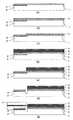
図3は、本発明の作製方法を説明するための図である。以下、密着層に感光性樹脂材料を使用した作製方法を図3を用いて具体的に説明する。 FIG. 3 is a diagram for explaining the manufacturing method of the present invention. Hereinafter, a manufacturing method using a photosensitive resin material for the adhesion layer will be specifically described with reference to FIGS.
なお、密着層6に使用する感光性樹脂材料としては、耐熱性を兼ね備えた感光性樹脂が好ましい。光導波路作製温度において変質、分解しないことが必要であり、耐熱性として、熱分解温度は300℃以上、より好ましくは350℃以上であることが望まれる。このような耐熱性を有した材料として、感光性ポリイミド等が好適である。さらに、密着性を考慮すると、フッ素を含有しない感光性ポリイミド等がより好適である。ポジ型、ネガ型いずれのタイプであっても構わない。 The photosensitive resin material used for the
まず、二酸化珪素膜を有するシリコン基板上にV溝3を形成する(a)。その後、基板上全面に感光性樹脂材料を塗布する(b)。プリベーク後、フォトマスクを使用して露光し、現像を行う。現像後、光導波路領域4にのみ感光性材料が残るように、感光性材料のポジ、ネガタイプにあわせたパターンのフォトマスクを使用する。このことにより、V溝領域5に塗布されていた感光性樹脂材料を選択的に除去することができる。フルキュア工程前の感光性樹脂材料の密着性は弱く、除去がより容易となり、V溝領域5にポリマー屑を残すことなく除去できる(c)。 First, a V-
その後、フルキュアにより光導波路領域4に残された感光性材料を硬化する。密着層6の厚さとしては、作製する光導波路の下部クラッド層7の厚さにもよるが、2μm以下、好ましくは1.5μm以下、より好ましくは1μm以下である。 Thereafter, the photosensitive material left in the
なお、感光性樹脂材料塗布前に、有機アルミニウム化合物、有機チタン化合物、有機ジルコニウム化合物などの有機金属化合物による密着層を形成しておいても良い。V溝領域5に形成された有機金属化合物による密着層は感光性材料をフルキュアにより硬化したのち、反応性イオンエッチングまたはフッ酸を用いたウエットエッチングにより除去できる。 Note that an adhesion layer made of an organometallic compound such as an organoaluminum compound, an organotitanium compound, or an organozirconium compound may be formed before application of the photosensitive resin material. The adhesion layer formed of the organometallic compound formed in the V-
引き続いて、光導波路を作製する。下部クラッド層7、コア層8を成膜し、フォトリソグラフィと反応性イオンエッチングの技法によりリッジ型コアパターンを形成し、さらに上部クラッド9を形成して導波路を埋め込むことにより、光導波路を作製する(d)。 Subsequently, an optical waveguide is manufactured. A
その後、光導波路上にマスクを作製し、V溝領域5に形成された樹脂層(下部クラッド、コア、上部クラッド層)を除去する(e)。マスクとしては、シリコン等の無機膜、有機レジストのいずれも使用できる。有機レジストの場合には、厚さ30μm程度におよぶV溝上に形成された樹脂層をエッチングしても光導波路上にレジストが残るよう厚さ調整することが必要である。マスク作製後、マスクが形成されていないV溝領域5に形成された樹脂層を反応性イオンエッチングにより除去する。この際、少なくともシリコン基板表面まではエッチングを行なう。V溝3内に残存する光導波路材料のポリイミドはフッ素を含んでおり、下地に密着層がないため、容易に除去することができる。さらに、密着層には感光性樹脂材料を使用しており、V溝内に塗布された感光性樹脂材料はフルキュア工程前、すなわち、プリベーク処理を行なったのみの段階の(感光性樹脂材料の密着性が十分発現されていない)、密着性の弱い状態で除去されているため、その除去は良好であり、作製プロセス終了後においても、V溝3内にポリマー屑をばらつきなく残すことなく、同一基板上に光導波路、V溝3を有したデバイスを作製できる。 Thereafter, a mask is formed on the optical waveguide, and the resin layers (lower clad, core, upper clad layer) formed in the V-
V溝領域5と光導波路領域4の境界に、光導波路の端面を切断する切込み溝10をダイシングにより作製し(f)、V溝に固定する光ファイバが光導波路と結合するようにする(g)。 A
この作製プロセスにおいては、従来行なわれてきたような密着層の除去方法、すなわち、フッ素を含有していない樹脂材料を塗布し、フルキュアを行い、その後に、レジストを使用して除去する方法とは異なり、レジストは不要となり、コスト削減にも繋がるとともに工程も簡略できる。 In this manufacturing process, a conventional method for removing an adhesion layer, that is, a method of applying a resin material not containing fluorine, performing a full cure, and then removing using a resist In contrast, no resist is required, leading to cost reduction and simplifying the process.
基板上に作製する光導波路パターンとしては、直線導波路、Y分岐導波路、方向性結合器、フィルタを挿入した波長合分波器などが挙げられるが、これに限定されるものではない。 Examples of the optical waveguide pattern produced on the substrate include, but are not limited to, a linear waveguide, a Y-branch waveguide, a directional coupler, and a wavelength multiplexer / demultiplexer in which a filter is inserted.
また、デバイス基板上に光導波路、V溝のみでなく、発光素子レーザダイオード、受光素子フォトダイオードが搭載できるように電極パターンを有するデバイスにおいても、上記作製方法により同様に作製できる。 A device having an electrode pattern so that not only an optical waveguide and a V-groove but also a light emitting element laser diode and a light receiving element photodiode can be mounted on the device substrate can be similarly manufactured by the above manufacturing method.
以下、実施例により説明する。 Hereinafter, an example explains.
4インチの熱酸化膜付き(1μm)シリコン基板を使用し、V溝付き光導波路を作製する。シリコン基板上の熱酸化膜をフォトリソグラフィとウエットエッチングにより加工した後、シリコンの異方性を利用し、ウエットエッチングによりV溝を作製した。次に、基板全面にフッ素を含まないネガ型感光性ポリイミド塗布し、プリベークを行なった。 Using a silicon substrate with a 4-inch thermal oxide film (1 μm), an optical waveguide with a V-groove is produced. After processing the thermal oxide film on the silicon substrate by photolithography and wet etching, a V groove was formed by wet etching using the anisotropy of silicon. Next, negative photosensitive polyimide not containing fluorine was applied to the entire surface of the substrate and prebaked.
その後、フォトマスクを介して、光導波路を作製する領域(V溝領域以外)に光があたるように露光し、現像を行なった。現像後、V溝領域の感光性ポリイミドは除去されており、その後加熱硬化し、光導波路を作製する領域にのみ1μm厚の密着層を形成した。 After that, exposure was performed through a photomask so that light was applied to a region (other than the V-groove region) for producing the optical waveguide, and development was performed. After development, the photosensitive polyimide in the V-groove region was removed, and then heat-cured to form an adhesion layer having a thickness of 1 μm only in the region for producing the optical waveguide.
続いて光導波路を作製した。光導波路に用いた樹脂はフッ素化ポリイミドである。密着層を形成した上記基板に、クラッド用のフッ素化ポリアミド酸ワニスをスピンコーティング装置により塗布した後、不活性雰囲気に保持したオーブンを用いて焼成して下部クラッド層を15μm成膜し、次にコア用フッ素化ポリアミド酸ワニスをスピンコーティング装置により塗布した後、不活性雰囲気に保持したオーブンを用いて焼成し、コア層を7μm成膜した。使用したコア層は屈折率が(1.51)であり、コア−クラッドの比屈折率差は0.33%とした。 Subsequently, an optical waveguide was produced. The resin used for the optical waveguide is fluorinated polyimide. After applying a fluorinated polyamic acid varnish for cladding to the substrate on which the adhesion layer has been formed using a spin coating apparatus, firing is performed using an oven maintained in an inert atmosphere to form a lower cladding layer of 15 μm, and then The core fluorinated polyamic acid varnish was applied by a spin coating apparatus and then baked using an oven kept in an inert atmosphere to form a core layer having a thickness of 7 μm. The core layer used had a refractive index of (1.51), and the core-clad relative refractive index difference was 0.33%.
このコア層上にマスク層としてシリコンをマグネトロンスパッタにより0.5μm成膜した。このマスク層上にはさらにレジスト層を成膜し、直線導波路のパターンをフォトマスクを用い、アライナによって露光し、パターニングされたレジスト層を形成した。 On the core layer, a silicon film having a thickness of 0.5 μm was formed by magnetron sputtering as a mask layer. A resist layer was further formed on the mask layer, and a linear waveguide pattern was exposed by an aligner using a photomask to form a patterned resist layer.
次にレジスト層に保護されていないマスク層のシリコンをRIE装置を用いて、CF4ガスを流入させながらエッチングした。引き続いてO2ガスを流入させてマスク層のシリコンに保護されていないコア層部分をエッチングにより除去し、次に、基板をフッ酸を含有する剥離液に浸漬し、マスク層を除去した。さらに下部クラッドと同種のフッ素化ポリイミド樹脂をスピンコーティング装置により塗布した後、不活性雰囲気に保持したオーブンを用いて焼成して、厚さ18ミクロンの上部クラッド層を形成した。コアのサイズは7×7μmである。Next, the silicon of the mask layer not protected by the resist layer was etched using a RIE apparatus while injecting CF4 gas. Subsequently, an O2 gas was allowed to flow to remove the core layer portion of the mask layer that was not protected by silicon, and then the substrate was immersed in a stripping solution containing hydrofluoric acid to remove the mask layer. Further, the same kind of fluorinated polyimide resin as that of the lower clad was applied by a spin coating apparatus and then baked using an oven maintained in an inert atmosphere to form an upper clad layer having a thickness of 18 microns. The core size is 7 × 7 μm.
次にV溝領域に形成された樹脂層(下部クラッド、コア、上部クラッド層)を除去した。基板全面にシリコンをマグネトロンスパッタにより0.5μm成膜した。このマスク層上にはさらにレジスト層を成膜し、フォトマスクを用い、アライナによって露光し、パターニングされたレジスト層を形成した。レジスト層はV溝領域以外に形成した。 Next, the resin layer (lower clad, core, upper clad layer) formed in the V-groove region was removed. A silicon film of 0.5 μm was formed on the entire surface of the substrate by magnetron sputtering. A resist layer was further formed on the mask layer, and was exposed by an aligner using a photomask to form a patterned resist layer. The resist layer was formed outside the V-groove region.
次にレジスト層に保護されていないマスク層のシリコンをRIE装置を用いて、CF4ガスを流入させながらエッチングした。引き続いてO2ガスを流入させてマスク層のシリコンに保護されていないV溝領域の樹脂層をエッチングにより除去した。この際、少なくともシリコン基板の表面が露出するまでエッチングを行なった。次に、基板をフッ酸を含有する剥離液に浸漬し、マスク層を除去した。Next, the silicon of the mask layer not protected by the resist layer was etched using a RIE apparatus while injecting CF4 gas. Subsequently, an O2 gas was introduced to remove the resin layer in the V-groove region that was not protected by silicon in the mask layer by etching. At this time, etching was performed until at least the surface of the silicon substrate was exposed. Next, the substrate was immersed in a stripping solution containing hydrofluoric acid to remove the mask layer.
V溝内の樹脂層は密着層が形成されていないため、剥離、除去されており、V溝内およびV溝周辺部の光導波路のない部分、いずれにおいても、ポリマー屑は認められず良好であった。また、バラツキもなかった。
(比較例1)
密着層形成にフッ素を含まない非感光性ポリイミドを使用した以外は、実施例1と同様に行なった。Since the adhesion layer is not formed on the resin layer in the V-groove, it is peeled off and removed, and in both the V-groove and the portion without the optical waveguide in the periphery of the V-groove, polymer debris is not recognized and is good. there were. There was no variation.
(Comparative Example 1)
The same procedure as in Example 1 was performed except that non-photosensitive polyimide containing no fluorine was used for forming the adhesion layer.
4インチの熱酸化膜付き(1μm)シリコン基板を使用し、V溝付き光導波路を作製した。シリコン基板上の熱酸化膜をフォトリソグラフィとウエットエッチングにより加工した後、シリコンの異方性を利用し、ウエットエッチングによりV溝を作製した。次に、基板全面にフッ素を含まない非感光性ポリイミド塗布し、加熱硬化し、基板全面に1μm厚の密着層を形成した。 Using a 4-inch thermal oxide film-attached (1 μm) silicon substrate, a V-grooved optical waveguide was produced. After processing the thermal oxide film on the silicon substrate by photolithography and wet etching, a V groove was formed by wet etching using the anisotropy of silicon. Next, a non-photosensitive polyimide containing no fluorine was applied to the entire surface of the substrate and cured by heating to form an adhesive layer having a thickness of 1 μm on the entire surface of the substrate.
以下、実施例1同様に、光導波路を作製し、V溝領域に形成された樹脂層(下部クラッド、コア、上部クラッド層)を除去した。 Thereafter, in the same manner as in Example 1, an optical waveguide was produced, and the resin layers (lower clad, core, upper clad layer) formed in the V-groove region were removed.
結果、V溝内の樹脂層は十分除去されておらず、V溝内にポリマー屑が認められ、不良であった。 As a result, the resin layer in the V-groove was not sufficiently removed, and polymer debris was observed in the V-groove, which was defective.
1 二酸化珪素膜
2 シリコン基板
3 V溝
4 光導波路領域
5 V溝領域
6 密着層
7 下部クラッド層
8 コア層
9 上部クラッド層
10 切込み溝
11 光ファイバDESCRIPTION OF
Claims (3)
Translated fromJapaneseAn optical waveguide device with a V groove manufactured by the manufacturing method according to claim 1.
Priority Applications (1)
| Application Number | Priority Date | Filing Date | Title |
|---|---|---|---|
| JP2005323937AJP2007133026A (en) | 2005-11-08 | 2005-11-08 | Method of manufacturing optical waveguide with v-groove |
Applications Claiming Priority (1)
| Application Number | Priority Date | Filing Date | Title |
|---|---|---|---|
| JP2005323937AJP2007133026A (en) | 2005-11-08 | 2005-11-08 | Method of manufacturing optical waveguide with v-groove |
Publications (1)
| Publication Number | Publication Date |
|---|---|
| JP2007133026Atrue JP2007133026A (en) | 2007-05-31 |
Family
ID=38154763
Family Applications (1)
| Application Number | Title | Priority Date | Filing Date |
|---|---|---|---|
| JP2005323937APendingJP2007133026A (en) | 2005-11-08 | 2005-11-08 | Method of manufacturing optical waveguide with v-groove |
Country Status (1)
| Country | Link |
|---|---|
| JP (1) | JP2007133026A (en) |
Cited By (2)
| Publication number | Priority date | Publication date | Assignee | Title |
|---|---|---|---|---|
| JP2012168267A (en)* | 2011-02-10 | 2012-09-06 | Hitachi Chem Co Ltd | Optical fiber connector and manufacturing method for the same |
| JP2012181266A (en)* | 2011-02-28 | 2012-09-20 | Hitachi Chem Co Ltd | Optical fiber connector and method of manufacturing the same |
- 2005
- 2005-11-08JPJP2005323937Apatent/JP2007133026A/enactivePending
Cited By (2)
| Publication number | Priority date | Publication date | Assignee | Title |
|---|---|---|---|---|
| JP2012168267A (en)* | 2011-02-10 | 2012-09-06 | Hitachi Chem Co Ltd | Optical fiber connector and manufacturing method for the same |
| JP2012181266A (en)* | 2011-02-28 | 2012-09-20 | Hitachi Chem Co Ltd | Optical fiber connector and method of manufacturing the same |
Similar Documents
| Publication | Publication Date | Title |
|---|---|---|
| KR100976671B1 (en) | Manufacturing method of optical waveguide | |
| CN102369467B (en) | Manufacture the method for optical waveguide core, the method manufacturing optical waveguide, optical waveguide and optoelectronic composite wiring board | |
| KR20040048312A (en) | Methods of forming waveguides and waveguides formed therefrom | |
| EP1662283B1 (en) | Process for producing a film optical waveguide | |
| JPH08286064A (en) | Polymer optical waveguide fabrication method | |
| CN102590943B (en) | The manufacture method of optical waveguide | |
| JP2007133026A (en) | Method of manufacturing optical waveguide with v-groove | |
| KR20000011817A (en) | Optical waveguide and manufacture thereof | |
| JP2002277663A (en) | Method for manufacturing optical waveguide | |
| JP4449075B2 (en) | Optical waveguide and method for manufacturing the same | |
| JP2003172836A (en) | Optical waveguide element with optical path alternation function | |
| JP2002311276A (en) | Method for forming resin optical waveguide | |
| WO2003091776A1 (en) | Resin optical waveguide and method for fabricating the same | |
| KR100322130B1 (en) | Optical Waveguide Forming Method | |
| JP4458328B2 (en) | Optical waveguide manufacturing method | |
| JP2005114746A (en) | Resin optical waveguide | |
| JP2001318257A (en) | Method for producing polymeric optical waveguide | |
| JP2006343516A (en) | Optical waveguide and method of forming the same | |
| JP2004021042A (en) | Opto-electric consolidated wiring board | |
| JP2005208187A (en) | Optical device having waveguide structure and its manufacturing method | |
| KR100491053B1 (en) | Method of manufacturing polymeric optical device | |
| JP2003279777A (en) | Manufacturing method of light guide device | |
| JP2002311278A (en) | Production method for resin optical waveguide | |
| JPWO2004025342A1 (en) | Device manufacturing method | |
| JP2006184864A (en) | Polymer optical waveguide manufacturing method and polymer optical waveguide |