JP2007123902A - Method of manufacturing rigid flexible printed circuit board - Google Patents
Method of manufacturing rigid flexible printed circuit boardDownload PDFInfo
- Publication number
- JP2007123902A JP2007123902AJP2006292679AJP2006292679AJP2007123902AJP 2007123902 AJP2007123902 AJP 2007123902AJP 2006292679 AJP2006292679 AJP 2006292679AJP 2006292679 AJP2006292679 AJP 2006292679AJP 2007123902 AJP2007123902 AJP 2007123902A
- Authority
- JP
- Japan
- Prior art keywords
- flexible
- region
- rigid
- circuit board
- printed circuit
- Prior art date
- Legal status (The legal status is an assumption and is not a legal conclusion. Google has not performed a legal analysis and makes no representation as to the accuracy of the status listed.)
- Pending
Links
- 238000004519manufacturing processMethods0.000titleclaimsabstractdescription64
- 238000000034methodMethods0.000claimsabstractdescription67
- RYGMFSIKBFXOCR-UHFFFAOYSA-NCopperChemical compound[Cu]RYGMFSIKBFXOCR-UHFFFAOYSA-N0.000claimsabstractdescription35
- 239000011889copper foilSubstances0.000claimsabstractdescription28
- 238000010030laminatingMethods0.000claimsabstractdescription8
- 239000000758substrateSubstances0.000claimsdescription16
- 230000001681protective effectEffects0.000claimsdescription12
- 238000005520cutting processMethods0.000claimsdescription9
- 238000003754machiningMethods0.000claimsdescription9
- 229920001721polyimidePolymers0.000claimsdescription8
- 238000000053physical methodMethods0.000claimsdescription7
- 238000004080punchingMethods0.000claimsdescription4
- 229910052802copperInorganic materials0.000abstractdescription7
- 239000010949copperSubstances0.000abstractdescription7
- 230000003247decreasing effectEffects0.000abstract1
- 239000010410layerSubstances0.000description60
- 238000007747platingMethods0.000description12
- 239000004065semiconductorSubstances0.000description11
- 238000003475laminationMethods0.000description4
- 238000005530etchingMethods0.000description3
- 230000010354integrationEffects0.000description3
- 238000011109contaminationMethods0.000description2
- 230000007547defectEffects0.000description2
- 238000010586diagramMethods0.000description2
- 238000007772electroless platingMethods0.000description2
- 238000009713electroplatingMethods0.000description2
- 238000005516engineering processMethods0.000description2
- 238000000206photolithographyMethods0.000description2
- 230000015572biosynthetic processEffects0.000description1
- 230000001413cellular effectEffects0.000description1
- 238000000576coating methodMethods0.000description1
- 238000010276constructionMethods0.000description1
- 238000007796conventional methodMethods0.000description1
- 230000000694effectsEffects0.000description1
- 239000003365glass fiberSubstances0.000description1
- 239000011810insulating materialSubstances0.000description1
- 239000011229interlayerSubstances0.000description1
- 239000000463materialSubstances0.000description1
- 238000012986modificationMethods0.000description1
- 230000004048modificationEffects0.000description1
- 238000000059patterningMethods0.000description1
- 230000000149penetrating effectEffects0.000description1
- 229920000728polyesterPolymers0.000description1
- 229920006267polyester filmPolymers0.000description1
- 230000007261regionalizationEffects0.000description1
- 239000011347resinSubstances0.000description1
- 229920005989resinPolymers0.000description1
- 239000000126substanceSubstances0.000description1
- 229920001187thermosetting polymerPolymers0.000description1
Images


Landscapes
- Engineering & Computer Science (AREA)
- Microelectronics & Electronic Packaging (AREA)
- Manufacturing & Machinery (AREA)
- Production Of Multi-Layered Print Wiring Board (AREA)
- Structure Of Printed Boards (AREA)
- Wire Bonding (AREA)
Abstract
Description
Translated fromJapanese本発明は、リジッドフレキシブルプリント基板の製造方法に係り、特に、外部接続端子用端子部を備えたフレキシブル領域及びリジッド領域を含むリジッドフレキシブルプリント基板の製造方法に関する。 The present invention relates to a method for manufacturing a rigid flexible printed circuit board, and more particularly, to a flexible region having a terminal portion for an external connection terminal and a method for manufacturing a rigid flexible printed circuit board including the rigid region.
最近は、半導体素子の高集積度化に伴い、半導体素子と外部回路とを接続するために半導体素子上に配設される接続端子の数が増大し、また配設密度も高くなっている趨勢にある。また、このような半導体素子が搭載される半導体パッケージなどの半導体装置においては、実装密度の向上などのために小型化、薄型化が求められており、特にノート型PC(personal computer)、PDA、携帯電話などの携帯型情報機器などに対応するための大きな課題は半導体パッケージの小型化、薄型化であるといえる。 Recently, as the degree of integration of semiconductor elements increases, the number of connection terminals provided on the semiconductor elements for connecting the semiconductor elements and external circuits has increased, and the arrangement density has increased. It is in. In addition, in a semiconductor device such as a semiconductor package on which such a semiconductor element is mounted, there is a demand for downsizing and thinning in order to improve the mounting density, and in particular, a notebook PC (personal computer), PDA, It can be said that a major problem in dealing with portable information devices such as cellular phones is the miniaturization and thinning of semiconductor packages.
半導体素子をパッケージングするには、半導体素子を配線基板上に搭載するとともに、半導体素子の接続端子と配線基板上の接続端子とを接続する必要がある。ところが、約10mm角程度の半導体素子の周囲に1000個程度の接続端子を配設する場合、その配設ピッチは約40μm程度と非常に微細なものになる。このような微細なピッチで配設された接続端子を、配線基板に配設された接続端子と接続するためには、配線基板上の配線形成または接続時の位置合わせに非常に高い精度が要求されるから、従来のワイヤボンディング(wire bonding)技術またはTAB(Tape Automated Bonding)技術では対応することが非常に難しいという問題点がある。 In order to package a semiconductor element, it is necessary to mount the semiconductor element on a wiring board and connect the connection terminal of the semiconductor element and the connection terminal on the wiring board. However, when about 1000 connection terminals are arranged around a semiconductor element of about 10 mm square, the arrangement pitch is as very fine as about 40 μm. In order to connect the connection terminals arranged at such a fine pitch to the connection terminals arranged on the wiring board, a very high accuracy is required for alignment on the wiring formation or connection on the wiring board. Therefore, there is a problem that it is very difficult to cope with conventional wire bonding technology or TAB (Tape Automated Bonding) technology.
かかる問題点を解決するための手段として、リジッド基板とフレキシブル基板とが構造的に結合して別途のコネクタの使用なしにリジッド領域とフレキシブル領域とが相互連結された構造を持つリジッドフレキシブルプリント基板(RFPCB;Rigid−Flexible Printed Circuit Board)の使用が益々増加しており、特に前記リジッドフレキシブルプリント基板は、モバイル機器の高機能化に伴う実装部品の高集積化とファインピッチの要求に対応してコネクタの使用による不要な空間を除去し、高集積化を要求する携帯電話などの小型端末機に主に用いられている。 As a means for solving such a problem, a rigid flexible printed circuit board having a structure in which a rigid board and a flexible board are structurally coupled and the rigid area and the flexible area are interconnected without using a separate connector ( The use of Rigid-Flexible Printed Circuit Board (RFPCB) is increasing, and in particular, the above-mentioned rigid flexible printed circuit board is a connector corresponding to the demand for higher integration of mounting parts and fine pitch accompanying the higher functionality of mobile devices. It is mainly used for small terminals such as mobile phones that require high integration by removing unnecessary space.
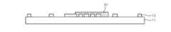
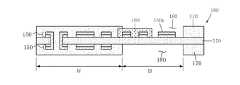
図1A〜図1Dは従来の一例に係るリジッドフレキシブルプリント基板の製造方法を示す工程図である。 1A to 1D are process diagrams showing a method for manufacturing a rigid flexible printed circuit board according to a conventional example.
まず、図1Aに示すように、ポリイミドフィルム11の一面に形成された第1回路パターン12のうちフレキシブル領域(図1Dの領域I参照)に対応する一部分をカバーレイ20で保護する。 First, as shown in FIG. 1A, a portion of the
その後、図1Bに示すように、フレキシブル領域の残りの対応回路パターン12領域にレジストカバー30を塗布してベース基板を形成する。第1回路パターン12のうちレジストカバー30で塗布された領域は、外部端子及び実装パッドのために露出される端子部であって、工程中に外部環境から保護するためにレジストカバー30を用いて保護する。 Thereafter, as shown in FIG. 1B, a
この際、レジストカバー30としては、耐熱テープまたはピーラブルインク(Peelable Ink)が使用できる。 At this time, as the resist cover 30, heat resistant tape or peelable ink can be used.
次いで、図1Cに示すように、ベース基板の両面に、フレキシブル領域に対応する開口部が形成された絶縁層40、及び開口部が形成された片面フレキシブル銅張積層板45、50を所定の加熱及び加圧のもとで積層する。 Next, as shown in FIG. 1C, the
片面フレキシブル銅張積層板45、50は、軟性フィルム45の一面に銅箔層50が形成されたものであり、軟性フィルム45は、ポリイミド系フィルムであることが好ましい。 The single-sided flexible copper-
その後、図1Dに示すように、銅箔層50に第2回路パターン80を形成し、端子部に形成されたレジストカバー30を除去して端子部を備えたフレキシブル領域I及びリジッド領域IIを含むリジッドフレキシブルプリント基板を完成する。 Thereafter, as shown in FIG. 1D, the second circuit pattern 80 is formed on the
この際、第2回路パターン80同士の間、及び第2回路パターン80と第1回路パターン12とを電気的に連結するためにスルーホール60を形成し、スルーホール60の内壁に導電性を与えるメッキ層70を形成する。 At this time, through
ここで、開口部を形成する軟性フィルム45の端部は、積層の際に受ける所定の圧力によって所定の角度をもって下方に垂れてしまう。 Here, the end portion of the
上述したように、従来のリジッドフレキシブルプリント基板の製造方法においては、外部端子及び実装パッドのために露出される端子部を製造工程中に外部環境から保護するためにレジストカバーを用いることにより、レジストカバー塗布工程及びレジストカバー除去工程をさらに行って工程コスト及び工程時間が増加するという問題点があった。 As described above, in the conventional method of manufacturing a rigid flexible printed circuit board, a resist cover is used to protect the terminal portion exposed for the external terminal and the mounting pad from the external environment during the manufacturing process. There is a problem that the process cost and the process time increase by further performing the cover coating process and the resist cover removing process.
また、端子部にレジストカバーを密着塗布し、いろいろの工程を行った後、レジストカバーを除去すると、端子部の表面にレジストカバーの残渣による汚染などの不良が発生するという問題点もあった。 Further, if the resist cover is applied to the terminal portion and various processes are performed and then the resist cover is removed, there is a problem in that a defect such as contamination due to the residue of the resist cover occurs on the surface of the terminal portion.
そこで、本発明はこのような問題点に鑑みてなされたもので、その目的とするところは、別途の保護手段を使用せずに、工程の順序を変更するだけで、外部端子及び実装パッドのために露出される端子部を保護することにより、工程コスト及び工程時間は減少させ且つ製品の信頼性は増加させた、リジッドフレキシブルプリント基板の製造方法を提供することにある。 Therefore, the present invention has been made in view of such problems, and the object of the present invention is to change the order of the external terminals and the mounting pads without using a separate protection means. Accordingly, it is an object of the present invention to provide a method for manufacturing a rigid flexible printed circuit board, in which process cost and process time are reduced and product reliability is increased by protecting the exposed terminal portion.
上記課題を解決するために、本発明のある観点によれば、フレキシブル領域とリジッド領域とを含むリジッドフレキシブルプリント基板の製造方法であって、(A)少なくとも一面に第1回路パターンが形成された第1軟性フィルムにおいてフレキシブル領域に対応する第1回路パターンの少なくとも一部分は保護フィルムで保護し、リジッド領域に対応する第1回路パターンの上面には絶縁層を積層してベース基板を形成する段階と、(B)第2軟性フィルムの一面に銅箔層が形成された片面フレキシブル銅張積層板を前記ベース基板の両面に積層する段階と、(C)フレキシブル領域に対応する銅箔層の部分は除去して第2軟性フィルムを露出させ、リジッド領域に対応する銅箔層の部分は第1回路パターンと連結される第2回路パターンを形成する段階と、(D)フレキシブル領域に対応する第2軟性フィルムの部分を除去する段階とを含むことを特徴とする、リジッドフレキシブルプリント基板の製造方法を提供する。 In order to solve the above problems, according to an aspect of the present invention, there is provided a method for manufacturing a rigid flexible printed board including a flexible region and a rigid region, wherein (A) a first circuit pattern is formed on at least one surface. Forming at least one portion of the first circuit pattern corresponding to the flexible region in the first flexible film with a protective film and laminating an insulating layer on the upper surface of the first circuit pattern corresponding to the rigid region; , (B) a step of laminating a single-sided flexible copper clad laminate having a copper foil layer formed on one surface of the second flexible film on both sides of the base substrate, and (C) a portion of the copper foil layer corresponding to the flexible region, The second circuit pattern is removed by exposing the second flexible film and the portion of the copper foil layer corresponding to the rigid region is connected to the first circuit pattern. Forming a provides (D), characterized in that it comprises a step of removing portions of the second flexible film corresponding to the flexible region, the manufacturing method of the rigid-flexible printed circuit board.
本発明に係るリジッドフレキシブルプリント基板の製造方法において、フレキシブル領域に対応する第1回路パターンにおける、保護フィルムで保護されていない領域は、外部接続端子用端子部であることを特徴とする。 In the method for manufacturing a rigid flexible printed circuit board according to the present invention, the region not protected by the protective film in the first circuit pattern corresponding to the flexible region is a terminal portion for external connection terminals.
また、本発明に係るリジッドフレキシブルプリント基板の製造方法において、(D)段階は、(D−1)第2軟性フィルムから、リジッド領域と接しないフレキシブル領域の端部と対応する領域をレーザ加工によって切断する段階と、(D−2)切断された第2軟性フィルムから、リジッド領域と接するフレキシブル領域の端部と対応する領域を物理的な方法で切断し、フレキシブル領域に対応する第2軟性フィルムを除去する段階とを含むことを特徴とする。 In the method for manufacturing a rigid flexible printed circuit board according to the present invention, in step (D), in step (D-1), from the second flexible film, a region corresponding to the end of the flexible region that does not contact the rigid region is formed by laser processing. A step of cutting, and (D-2) a second flexible film corresponding to the flexible region by cutting the region corresponding to the end of the flexible region in contact with the rigid region from the cut second flexible film by a physical method And a step of removing.
また、本発明に係るリジッドフレキシブルプリント基板の製造方法において、第1回路パターンは、リジッド領域と接しないフレキシブル領域の端部と対応する領域に形成された境界パターンを含んでレーザ加工の際に第1軟性フィルムを保護し、ここで、境界パターンは第1回路パターン内の他のパターンと電気的に連結されないことを特徴とする。 In the method of manufacturing a rigid flexible printed circuit board according to the present invention, the first circuit pattern includes a boundary pattern formed in a region corresponding to an end portion of the flexible region that is not in contact with the rigid region. One flexible film is protected, wherein the boundary pattern is not electrically connected to other patterns in the first circuit pattern.
また、本発明に係るリジッドフレキシブルプリント基板の製造方法において、(D)段階は、レーザ加工によって、フレキシブル領域に対応する第2軟性フィルムの部分を除去することを特徴とする。 In the method for manufacturing a rigid flexible printed circuit board according to the present invention, the step (D) is characterized by removing a portion of the second flexible film corresponding to the flexible region by laser processing.
また、本発明に係るリジッドフレキシブルプリント基板の製造方法において、(D)段階は、(D−1)第2軟性フィルムから、リジッド領域と接しないフレキシブル領域IIIの端部と対応する領域を機械加工によって切断する段階と、(D−2)切断された第2軟性フィルムから、リジッド領域と接するフレキシブル領域の端部と対応する領域を物理的な方法で切断して、フレキシブル領域に対応する第2軟性フィルムを除去する段階とを含むことを特徴とする。 Moreover, in the manufacturing method of the rigid flexible printed circuit board which concerns on this invention, (D) step machined the area | region corresponding to the edge part of the flexible area | region III which does not contact a rigid area | region from (D-1) 2nd flexible film. And (D-2) cutting the second flexible film corresponding to the flexible region by cutting the region corresponding to the end of the flexible region in contact with the rigid region from the cut second flexible film by a physical method. Removing the flexible film.
また、本発明に係るリジッドフレキシブルプリント基板の製造方法において、(D)段階は、フレキシブル領域に対応する第2軟性フィルムの部分を機械加工によって除去することを特徴とする。 In the method for manufacturing a rigid flexible printed circuit board according to the present invention, the step (D) is characterized in that a portion of the second flexible film corresponding to the flexible region is removed by machining.
また、本発明に係るリジッドフレキシブルプリント基板の製造方法において、機械加工はパンチング、ナイフ、ルータービットのいずれか一つを使用した加工であることを特徴とする。 In the method for manufacturing a rigid flexible printed circuit board according to the present invention, the machining is a process using any one of punching, a knife, and a router bit.
また、本発明に係るリジッドフレキシブルプリント基板の製造方法において、第1軟性フィルム及び第2軟性フィルムはポリイミド系フィルムであることを特徴とする。 In the method for manufacturing a rigid flexible printed board according to the present invention, the first flexible film and the second flexible film are polyimide films.
また、本発明に係るリジッドフレキシブルプリント基板の製造方法において、絶縁層は半硬化状態のプリプレグであることを特徴とする。 In the method for manufacturing a rigid flexible printed board according to the present invention, the insulating layer is a semi-cured prepreg.
また、本発明に係るリジッドフレキシブルプリント基板の製造方法において、絶縁層はボンディングシートであることを特徴とする。 In the method for manufacturing a rigid flexible printed board according to the present invention, the insulating layer is a bonding sheet.
また、本発明に係るリジッドフレキシブルプリント基板の製造方法において、(A)段階の後、(E)絶縁層の上面に追加の回路層及び追加の絶縁層を交互に所望の数だけ形成する段階をさらに含むことを特徴とする。 In the method of manufacturing a rigid flexible printed circuit board according to the present invention, after the step (A), (E) a step of alternately forming a desired number of additional circuit layers and additional insulating layers on the upper surface of the insulating layer. It is further characterized by including.
本発明のリジッドフレキシブルプリント基板の製造方法によれば、別途の保護物質を使用せずに、工程の順序を変更するだけで、外部端子及び実装パッドのために露出される端子部を保護することにより、工程コスト及び工程時間は減少させ且つ製品の信頼性は増加させることができる。 According to the method of manufacturing the rigid flexible printed circuit board of the present invention, the external terminal and the terminal portion exposed for the mounting pad can be protected by changing the order of the processes without using a separate protective substance. As a result, the process cost and the process time can be reduced and the reliability of the product can be increased.
以下に添付図面を参照しながら、本発明の好適な実施の形態について詳細に説明する。 Exemplary embodiments of the present invention will be described below in detail with reference to the accompanying drawings.
図2及び図3は本発明に係るリジッドフレキシブルプリント基板の製造方法を示す図であり、図2は本発明に係るリジッドフレキシブルプリント基板の製造方法を示す順序図、図3A〜図3Iは本発明に係るリジッドフレキシブルプリント基板の製造方法を詳細に示す工程断面図である。 2 and 3 are views showing a method for manufacturing a rigid flexible printed circuit board according to the present invention, FIG. 2 is a flow chart showing the method for manufacturing a rigid flexible printed circuit board according to the present invention, and FIGS. It is process sectional drawing which shows the manufacturing method of the rigid flexible printed circuit board concerning this in detail.
図2を参照して本発明に係るリジッドフレキシブルプリント基板の製造方法を説明すると、次の通りである。 A method for manufacturing a rigid flexible printed circuit board according to the present invention will be described with reference to FIG.
まず、少なくとも一面に第1回路パターンが形成された第1軟性フィルムにおいて、フレキシブル領域IIIに対応する第1回路パターンの一部分は保護フィルムで保護し、リジッド領域IVに対応する第1回路パターンの上面には絶縁層を積層してベース基板を形成する(S100)。 First, in the first flexible film having the first circuit pattern formed on at least one surface, a part of the first circuit pattern corresponding to the flexible region III is protected by a protective film, and the upper surface of the first circuit pattern corresponding to the rigid region IV In step S100, an insulating layer is stacked to form a base substrate.
この際、フレキシブル領域IIIに対応する第1回路パターンにおいて、外部接続端子用端子部を除いた第1回路パターンは外部環境から保護するために保護フィルムで保護し、端子部はそのまま露出させる。保護フィルムとしては、例えばポリイミド系フィルムのような柔軟性のあるフィルムを使用することが好ましい。 At this time, in the first circuit pattern corresponding to the flexible region III, the first circuit pattern excluding the terminal portion for external connection terminal is protected with a protective film to protect it from the external environment, and the terminal portion is exposed as it is. As the protective film, it is preferable to use a flexible film such as a polyimide film.
本発明の一実施例に係るリジッドフレキシブルプリント基板の製造方法においては、リジッド領域IVに対応する第1回路パターンの上面に形成された絶縁層に追加の回路層及び絶縁層を交互に所望の数だけ更に積層して多層化したベース基板を形成することができる。 In the method of manufacturing the rigid flexible printed circuit board according to the embodiment of the present invention, a desired number of additional circuit layers and insulating layers are alternately formed on the insulating layer formed on the upper surface of the first circuit pattern corresponding to the rigid region IV. Thus, it is possible to form a base substrate having a multilayer structure.
その後、ベース基板の両面に片面フレキシブル銅張積層板を順次積層する(S200)。 Thereafter, a single-sided flexible copper-clad laminate is sequentially laminated on both sides of the base substrate (S200).
この際、片面フレキシブル銅張積層板は、第2軟性フィルムの一面に銅箔層が形成された形であって、実施例によっては第2軟性フィルムと銅箔層とを分離して積層してもよい。 At this time, the single-sided flexible copper-clad laminate has a shape in which a copper foil layer is formed on one surface of the second flexible film. In some embodiments, the second flexible film and the copper foil layer are separated and laminated. Also good.
次いで、フレキシブル領域IIIに対応する銅箔層の部分は除去して第2軟性フィルムを露出させ、リジッド領域IVに対応する部分は第1回路パターンと連結される第2回路パターンを形成する(S300)。 Next, the portion of the copper foil layer corresponding to the flexible region III is removed to expose the second flexible film, and the portion corresponding to the rigid region IV forms a second circuit pattern connected to the first circuit pattern (S300). ).
すなわち、リジッド領域IVに対応する銅箔層にスルーホールを形成し、無電解銅メッキ及び電解銅メッキを施してスルーホール内に導電性を与えた後、エッチング工程を行い、フレキシブル領域IIIに対応する銅箔層は除去し、リジッド領域IVに対応する銅箔層に第2回路パターンを形成する。この際、第2回路パターンはスルーホールによって第1回路パターンと電気的に連結できる。 In other words, a through hole is formed in the copper foil layer corresponding to the rigid region IV, electroless copper plating and electrolytic copper plating are applied to provide conductivity in the through hole, and then an etching process is performed to cope with the flexible region III. The copper foil layer to be removed is removed, and a second circuit pattern is formed on the copper foil layer corresponding to the rigid region IV. At this time, the second circuit pattern can be electrically connected to the first circuit pattern through a through hole.
最後に、フレキシブル領域IIIに対応する第2軟性フィルムの部分を除去する(S400)。 Finally, the portion of the second flexible film corresponding to the flexible region III is removed (S400).
第2軟性フィルムにレーザ加工または機械加工を行い、フレキシブル領域IIIに対応する部分を一挙に除去することができる。このとき、レーザ加工の際に、第1軟性フィルムに損傷を与えることなく第2軟性フィルムのみを除去し得るように深さを調節することができる。 The second flexible film can be laser-processed or machined to remove portions corresponding to the flexible region III all at once. At this time, the depth can be adjusted so that only the second flexible film can be removed without damaging the first flexible film during laser processing.
または、本発明の他の実施例によって、リジッド領域IVと接しないフレキシブル領域IIIの端部に対応する第2軟性フィルムの領域をレーザ加工または機械加工によって切断し、残りのリジッド領域IVと接するフレキシブル領域IIIの端部に対応する第2軟性フィルムの領域を物理的な方法で除去して、フレキシブル領域IIIに対応する第2軟性フィルムを除去することができる。 Alternatively, according to another embodiment of the present invention, the region of the second flexible film corresponding to the end of the flexible region III that is not in contact with the rigid region IV is cut by laser processing or machining, and the flexible contact with the remaining rigid region IV is performed. The area | region of the 2nd flexible film corresponding to the edge part of the area | region III can be removed by a physical method, and the 2nd flexible film corresponding to the flexible area | region III can be removed.
このとき、レーザ加工の際に、第1軟性フィルムに損傷を与えることなく第2軟性フィルムのみを切断し得るように、第1回路パターンがリジッド領域IVと接しないフレキシブル領域IIIの端部と対応する領域に形成された境界パターンを含み、境界パターンは、第1回路パターン内の他のパターンと電気的に連結されないように形成され得る。 At this time, the first circuit pattern corresponds to the end of the flexible region III that does not contact the rigid region IV so that only the second flexible film can be cut without damaging the first flexible film during laser processing. The boundary pattern may be formed so as not to be electrically connected to other patterns in the first circuit pattern.
上述したように、本発明に係るリジッドフレキシブルプリント基板の製造方法においては、フレキシブル領域III内の端子部を別途の保護手段を用いて保護せず、外層を形成するために積層された第2軟性フィルム及び銅箔層の開口部形成工程の時期を第2回路パターン形成の後に変更して端子部を保護することにより、工程数及び工程コストの増加なしに製品の信頼性を向上させることができる。 As described above, in the method for manufacturing a rigid flexible printed circuit board according to the present invention, the second flexible layer laminated to form the outer layer without protecting the terminal portion in the flexible region III using a separate protection means. By changing the timing of the film and copper foil layer opening forming step after the second circuit pattern formation to protect the terminal portion, the reliability of the product can be improved without increasing the number of steps and the process cost. .
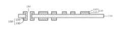
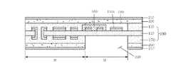
図3A〜図3Iは、本発明の一実施例に係るリジッドフレキシブルプリント基板を製造する方法の一例を示す工程図である。 3A to 3I are process diagrams illustrating an example of a method for manufacturing a rigid flexible printed circuit board according to an embodiment of the present invention.
まず、図3Aに示すように、第1軟性フィルム110の両面に銅箔層120が形成されたフレキシブル銅張積層板(Flexible PCB)100を提供する。 First, as shown in FIG. 3A, a flexible copper clad laminate (Flexible PCB) 100 in which copper foil layers 120 are formed on both surfaces of a first
第1軟性フィルム110としては、例えばポリエステルまたはポリイミドフィルムを使用することができる。 As the 1st
その後、図3Bに示すように、第1軟性フィルム100の両面に、互いに電気的に連結される第1回路パターン150を形成する。 Thereafter, as shown in FIG. 3B,
すなわち、フレキシブル銅張積層板100を貫通する内部ビアホール130を形成し、無電解メッキ及び電解メッキを施してメッキ層140を形成した後、メッキ層140の形成された銅箔層120に例えばフォトリソグラフィー工法を施して第1回路パターン150を形成することができる。この際、両面に形成された第1回路パターン150は、メッキ層140によって導電性が与えられた内部ビアホール130に沿って互いに電気的に連結できる。 That is, an internal via
ここで、第1回路パターン150はフレキシブル領域(図3Eの領域III参照)内の外部接続端子用端子部150aを含み、フレキシブル領域においては、第1軟性フィルム110の一面(図中上面)にのみ第1回路パターン150が形成されていて、他面(図中下面)には第1回路パターンが配置されてない。 Here, the
次に、図3Cに示すように、端子部150aを除いたフレキシブル領域に対応する第1回路パターン150の上面に保護フィルム160を塗布する。 Next, as shown in FIG. 3C, a
端子部150aを除いたフレキシブル領域に対応する第1回路パターン150を外部環境から保護するために、例えばポリイミドフィルムのような柔軟性のあるフィルムを保護フィルムとして用いて第1回路パターン150の上面に密着塗布することにより、第1回路パターン150を保護するようにする。 In order to protect the
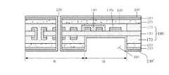
その後、図3Dに示すように、フレキシブル領域に対応する開口部180が形成された絶縁層170を提供する。 Thereafter, as shown in FIG. 3D, an insulating
絶縁層170は、ガラス繊維に熱硬化性樹脂を浸透させて半硬化状態にしたプリプレグまたはボンディングシートを採用し、積層時には層間接着力を高め、積層後にはリジッド領域の物理的強度を高めることができる。 The insulating
開口部180は、木型、金型などを用いたパンチング加工またはルーター加工などで形成することができる。 The
次いで、図3Eに示すように、第1回路パターン150の一部が保護フィルム160によって保護された第1軟性フィルム110の両面に、各々に開口部180が形成された各絶縁層170をそれぞれ積層して、フレキシブル領域III及び予備リジッド領域IVを含むベース基板190を形成する。 Next, as shown in FIG. 3E, the insulating
本発明の他の実施例に係るリジッドフレキシブルプリント基板の製造方法においては、絶縁層170の上面に追加の回路層(図示せず)及び絶縁層を交互に所望の数だけさらに積層して多層化されたベース基板を形成することができる。 In the method of manufacturing a rigid flexible printed circuit board according to another embodiment of the present invention, a desired number of additional circuit layers (not shown) and insulating layers are alternately stacked on the upper surface of the insulating
ここで、第1回路パターン150及び第1軟性フィルム110のうち絶縁層170の開口部180に露出された領域はフレキシブル領域IIIを形成し、絶縁層170が積層されて機械的強度が増加した領域は予備リジッド領域IVを形成する。 Here, a region of the
その後、図3Fに示すように、ベース基板190の両面に片面フレキシブル銅張積層板(200、210)(200’、210’)を積層する。 Thereafter, as shown in FIG. 3F, single-sided flexible copper-clad laminates (200, 210) (200 ', 210') are laminated on both sides of the
ここで、片面フレキシブル銅張積層板(200、210)(200’、210’)は、第2軟性フィルム200、200’の一面に銅箔層210、210’が形成されたものである。 Here, the single-sided flexible copper-clad laminate (200, 210) (200 ', 210') is obtained by forming copper foil layers 210, 210 'on one surface of the second
ベース基板190の一面において、開口部180が形成された絶縁層170によって露出された端子部150aは、開口部のない片面フレキシブル銅張積層板200、210によって、リジッドフレキシブルプリント基板が完成されるまで外部環境から保護できるようにする。即ち、第1回路パターン150のうちフレキシブル領域IIIに存在する部分及び端子部150aは、開口部180の上面を塞ぐように設けられた片面フレキシブル銅張積層板(200、210)によって覆われる。 On one surface of the
この際、ベース基板190の他面において、第1軟性フィルム110の上面(図3Fでは下側に向く面)には、開口部180を有するもう一つの絶縁層170を積層し、更にこの絶縁層170上に、片面フレキシブル銅張積層板(200’、210’)を積層する。前記片面フレキシブル銅張積層板(200’、210’)は、前記開口部180に対応して貫通形成された開口部220を有する。従って、第1軟性フィルム110のフレキシブル領域IIIに位置する前記第1回路パターン150が形成されてない下側の面は、互いに重なり合っている前記開口部180と220とにより露出された状態となっている。第2軟性フィルム200、200’は、第1軟性フィルム110と同様に、例えばポリエステルまたはポリイミドフィルムで形成できる。 At this time, on the other surface of the
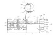
次いで、図3Gに示すように、予備リジッド領域IVの一部において、ベース基板190及びその両面に積層された銅箔層210、210’を貫通するスルーホール230を形成し、スルーホール230の内部及び各銅箔層210、210’の上面にメッキ層240、240’を形成する。なお、メッキ層240’は、開口部220から露出する部分にも形成される。 Next, as shown in FIG. 3G, in a part of the preliminary rigid region IV, a through
銅箔層210に形成される第2回路パターン(図3Hの250参照)を第1回路パターン150と電気的に連結するために形成されたスルーホール230は、内部に第1軟性フィルム110、絶縁層170及び第2軟性フィルム200、200’などの絶縁物質を含んでいるため、無電解メッキ及び電解メッキを施してメッキ層240、240’を形成することにより、スルーホール230の内部に導電性を与えることができる。 The through
この際、スルーホール230は、CNCドリル(Computer Numerical Control Drill)などの機械ドリルを用いて、予め設定された位置に基づいて形成される。 At this time, the through
実施例において、メッキ層240、240’が内壁に形成されたスルーホール230内を埋め込み用インク(図示せず)で充填させることができる。 In the embodiment, the through
その後、図3Hに示すように、メッキ層240が形成された銅箔層210において、フレキシブル領域IIIに対応する部分は除去し、また、予備リジッド領域IVに対応するメッキ層240、240’が形成された銅箔層210、210’に第2回路パターン250、250’を形成してリジッド領域Vを完成する。 Thereafter, as shown in FIG. 3H, a portion corresponding to the flexible region III is removed from the
第2回路パターン250、250’は、例えば、メッキ層240、240’の上面に感光性物質(図示せず)を塗布し、パターンが形成されたアートワークフィルムを密着させた後、露光及び現像工程を行ってエッチングレジストパターンを形成し、エッチング工程を行うフォトリソグラフィー工法を用いて形成することができる。 For example, the
ここで、第2回路パターン250は、スルーホール230によって第1回路パターン150及び他面の第2回路パターン250’と電気的に連結できる。 Here, the
最後に、図3Iに示すように、フレキシブル領域IIIに対応する部分の第2軟性フィルム200を除去することにより、フレキシブル領域III及びリジッド領域Vを含むリジッドフレキシブルプリント基板を形成する。 Finally, as shown in FIG. 3I, a portion of the second
ここで、第2軟性フィルム200を部分的に除去する方法としては、図3Hを平面図で表す図4に示すように、第2軟性フィルム200において、リジッド領域Vと接しないフレキシブル領域IIIの端部に対応する領域Aはレーザ加工または機械加工を行って切断し、リジッド領域Vに接するフレキシブル領域IIIの端部に対応する領域Bは物理的な方法で除去して、フレキシブル領域IIIに対応する第2軟性フィルム200を除去することができる。この物理的除去方法としては、例えば、前記切断により舌片状となっている第2軟性フィルム200の根元の前記領域Bに沿う銅箔層のエッジにおいて、その舌片を斜め上方に引き上げながら切り取るようにして除去する簡単な方法を採用することができる。 Here, as a method of partially removing the second
上述したように、第2軟性フィルム200において、リジッド領域Vと接するフレキシブル領域IIIの端部に対応する領域Bを物理的な方法で除去すると、第2軟性フィルム200の端部は、物理的な方法の使用の際に発生する所定の圧力によって所定の角度を持って上方に向かうので、図1Dに示すように、従来の開口部を形成した後に軟性フィルム45の端部と反対の形状を持つ。 As described above, when the region B corresponding to the end of the flexible region III in contact with the rigid region V is removed by the physical method in the second
また、レーザ加工の際に、第1軟性フィルム110に損傷を与えることなく第2軟性フィルム200のみを切断し得るように、第1回路パターン150にはリジッド領域Vと接しないフレキシブル領域IIIの端部と対応する領域Aに境界パターン(図示せず)をさらに形成することができる。ここで、境界パターンは、第1回路パターン150内の他のパターンと電気的に連結されないように形成しなければならない。前記境界パターンは、第1回路パターン150内の不所望な電気的短絡及び切断時の第1軟性フィルムの損傷を避けるように、例えば、第1回路パターンと共に銅箔層のパターニングによって、電気的にはダミーなパターンとして形成することができる。 In addition, at the time of laser processing, the
または、本発明の他の実施例に係るリジッドフレキシブルプリント基板の製造方法によって、レーザ加工または機械加工を行い、フレキシブル領域IIIに対応する第2軟性フィルム200を一挙に除去することができる。このとき、レーザ加工の際に、第1軟性フィルム110に損傷を与えることなく第2軟性フィルム200のみを除去し得るように、深さを調節することができる。 Alternatively, the second
ここで、機械加工は、パンチング、ナイフ、ルータービットなどを使用する加工であることが好ましい。 Here, the machining is preferably a process using punching, a knife, a router bit, or the like.
従来のリジッドフレキシブルプリント基板の製造方法においては、フレキシブル領域内の外部端子または実装パッドのための端子部を製造工程中に外部環境から保護するために、耐熱テープやピーラブルインクなどを用いて端子部にレジストカバーを形成し、製造工程の後にレジストカバーを除去することにより、残渣による汚染などによって製品の不良をもたらし、レジストカバーの形成及び除去による工程の追加によってコスト及び時間が増加するという問題点があった。 In a conventional rigid flexible printed circuit board manufacturing method, a terminal using heat-resistant tape or peelable ink is used to protect the external terminal in the flexible region or the terminal portion for the mounting pad from the external environment during the manufacturing process. Forming a resist cover on the part and removing the resist cover after the manufacturing process brings about product defects due to contamination by residues, etc., and increases in cost and time due to the addition of the process by forming and removing the resist cover There was a point.
ところが、上述したように、本発明に係るリジッドフレキシブルプリント基板の製造方法においては、別途の保護手段を使用せずに、工程の順序を変更するだけで、外部端子及び実装パッドのために露出される端子部を保護することにより、工程コスト及び工程時間は減少させ且つ製品の信頼性は増加させる効果をもたらすことができる。 However, as described above, in the method of manufacturing the rigid flexible printed circuit board according to the present invention, the external terminals and the mounting pads are exposed only by changing the order of the processes without using a separate protection means. By protecting the terminal portion, the process cost and the process time can be reduced and the reliability of the product can be increased.
すなわち、リジッド領域の第2回路パターン形成のための片面フレキシブル銅張積層板の積層の際に、フレキシブル領域に対応する開口部を、積層の前に形成せず、第2回路パターンの形成後に形成することにより、外部に露出された端子部を製造工程中に別途の保護手段なしに保護することができるので、工程の単純化を実現しながら製品の信頼性を向上させる効果をもたらすことができる。 That is, when laminating the single-sided flexible copper-clad laminate for forming the second circuit pattern in the rigid region, the opening corresponding to the flexible region is not formed before the lamination, but is formed after the second circuit pattern is formed. By doing so, it is possible to protect the terminal portion exposed to the outside without a separate protection means during the manufacturing process, and thus it is possible to bring about an effect of improving the reliability of the product while realizing simplification of the process. .
以上、本発明を特定の実施例によって詳細に説明したが、これら実施例は本発明の範囲を限定するものではなく、本発明の範囲内において、各種変形を加えることができる。本発明の範囲は、特許請求の範囲の解釈によってのみ限定される。 As mentioned above, although this invention was demonstrated in detail by the specific Example, these Examples do not limit the scope of the present invention, Various modifications can be added within the scope of the present invention. The scope of the invention is limited only by the interpretation of the claims.
100 フレキシブル銅張積層板
110 第1軟性フィルム
120、210、210’ 銅箔層
130 内部ビアホール
140、240、240’ メッキ層
150 内部回路パターン
150a 端子部
160 保護フィルム
170 絶縁層
180、220 開口部
190 ベース基板
200、200’ 第2軟性フィルム
230 スルーホール
250、250’ 第2回路パターンDESCRIPTION OF
Claims (12)
Translated fromJapanese(A)少なくとも一面に第1回路パターンが形成された第1軟性フィルムにおいて、前記フレキシブル領域に対応する第1回路パターンの少なくとも一部分は保護フィルムで保護し、前記リジッド領域に対応する第1回路パターンの上面には絶縁層を積層してベース基板を形成する段階と、
(B)第2軟性フィルムの一面に銅箔層が形成された片面フレキシブル銅張積層板を前記ベース基板の両面に積層する段階と、
(C)前記フレキシブル領域に対応する前記銅箔層の部分は除去して前記第2軟性フィルムを露出させ、前記リジッド領域に対応する前記銅箔層の部分には前記第1回路パターンと連結される第2回路パターンを形成する段階と、
(D)前記フレキシブル領域に対応する前記第2軟性フィルムの部分を除去する段階と、を含むことを特徴とする、リジッドフレキシブルプリント基板の製造方法。A method for manufacturing a rigid flexible printed circuit board including a flexible region and a rigid region,
(A) In the first flexible film having a first circuit pattern formed on at least one surface, at least a part of the first circuit pattern corresponding to the flexible region is protected by a protective film, and the first circuit pattern corresponding to the rigid region Forming a base substrate by laminating an insulating layer on the upper surface of the substrate,
(B) Laminating a single-sided flexible copper-clad laminate having a copper foil layer formed on one side of the second flexible film on both sides of the base substrate;
(C) The portion of the copper foil layer corresponding to the flexible region is removed to expose the second flexible film, and the portion of the copper foil layer corresponding to the rigid region is connected to the first circuit pattern. Forming a second circuit pattern comprising:
(D) removing the portion of the second flexible film corresponding to the flexible region, and a method for producing a rigid flexible printed circuit board.
(D−1)前記第2軟性フィルムから、前記リジッド領域と接しない前記フレキシブル領域の端部と対応する領域をレーザ加工によって切断する段階と、
(D−2)前記切断された第2軟性フィルムから、前記リジッド領域と接する前記フレキシブル領域の端部と対応する領域を物理的な方法で切断して、フレキシブル領域に対応する第2軟性フィルムを除去する段階とを含むことを特徴とする、請求項1に記載のリジッドフレキシブルプリント基板の製造方法。In step (D),
(D-1) cutting the region corresponding to the end of the flexible region not in contact with the rigid region by laser processing from the second flexible film;
(D-2) From the cut second flexible film, a region corresponding to the end of the flexible region in contact with the rigid region is cut by a physical method, and a second flexible film corresponding to the flexible region is obtained. The manufacturing method of the rigid flexible printed circuit board of Claim 1 including the step of removing.
(D−1)前記第2軟性フィルムから、前記リジッド領域と接しない前記フレキシブル領域IIIの端部と対応する領域を機械加工によって切断する段階と、
(D−2)前記切断された第2軟性フィルムから、リジッド領域と接するフレキシブル領域の端部と対応する領域を物理的な方法で切断して、前記フレキシブル領域に対応する第2軟性フィルムを除去する段階とを含むことを特徴とする、請求項1に記載のリジッドフレキシブルプリント基板の製造方法。In step (D),
(D-1) cutting the region corresponding to the end of the flexible region III that does not contact the rigid region by machining from the second flexible film;
(D-2) The second flexible film corresponding to the flexible region is removed from the cut second flexible film by cutting the region corresponding to the end of the flexible region in contact with the rigid region by a physical method. The manufacturing method of the rigid flexible printed circuit board of Claim 1 characterized by including the step to perform.
(E)前記絶縁層の上面に追加の回路層及び追加の絶縁層を交互に所望の数だけ形成する段階をさらに含むことを特徴とする、請求項1に記載のリジッドフレキシブルプリント基板の製造方法。After the step (A),
2. The method of manufacturing a rigid flexible printed circuit board according to claim 1, further comprising the step of alternately forming a desired number of additional circuit layers and additional insulating layers on the upper surface of the insulating layer. .
Applications Claiming Priority (1)
| Application Number | Priority Date | Filing Date | Title |
|---|---|---|---|
| KR1020050102464AKR100722621B1 (en) | 2005-10-28 | 2005-10-28 | Manufacturing method of flexible printed circuit board |
Publications (1)
| Publication Number | Publication Date |
|---|---|
| JP2007123902Atrue JP2007123902A (en) | 2007-05-17 |
Family
ID=38063640
Family Applications (1)
| Application Number | Title | Priority Date | Filing Date |
|---|---|---|---|
| JP2006292679APendingJP2007123902A (en) | 2005-10-28 | 2006-10-27 | Method of manufacturing rigid flexible printed circuit board |
Country Status (4)
| Country | Link |
|---|---|
| JP (1) | JP2007123902A (en) |
| KR (1) | KR100722621B1 (en) |
| CN (1) | CN100551206C (en) |
| TW (1) | TWI300678B (en) |
Cited By (3)
| Publication number | Priority date | Publication date | Assignee | Title |
|---|---|---|---|---|
| JP2010021297A (en)* | 2008-07-10 | 2010-01-28 | Compeq Manufacturing Co Ltd | Rigid flex circuit board comprising peelable protective layer and manufacturing method thereof |
| CN103635007A (en)* | 2012-08-24 | 2014-03-12 | 富葵精密组件(深圳)有限公司 | Rigid-flexible circuit substrate, rigid-flexible circuit board and manufacturing method thereof |
| CN108012453A (en)* | 2017-12-07 | 2018-05-08 | 江门黑氪光电科技有限公司 | A kind of multilayer circuit board fabrication method for LED light strip |
Families Citing this family (10)
| Publication number | Priority date | Publication date | Assignee | Title |
|---|---|---|---|---|
| KR100993318B1 (en)* | 2008-09-04 | 2010-11-09 | 삼성전기주식회사 | Manufacturing method of flexible printed circuit board in the form of flying tail |
| TWI496518B (en)* | 2009-10-02 | 2015-08-11 | Innolux Corp | Flexible printed circuit board and method for forming monitor |
| KR101055514B1 (en)* | 2009-12-03 | 2011-08-08 | 삼성전기주식회사 | Manufacturing method of rigid-flexible substrate |
| US8493747B2 (en)* | 2010-02-05 | 2013-07-23 | Ibiden Co., Ltd. | Flex-rigid wiring board and method for manufacturing the same |
| KR101387313B1 (en)* | 2012-02-21 | 2014-04-18 | 삼성전기주식회사 | Method of manufacturing flying tail type rigid-flexible printed circuit board and flying tail type rigid-flexible printed circuit board manufactured by the same |
| KR101814113B1 (en)* | 2012-11-02 | 2018-01-02 | 삼성전기주식회사 | Method for manufacturing of printed circuit board |
| CN103384444B (en)* | 2013-07-30 | 2016-04-20 | 博敏电子股份有限公司 | A kind ofly protect rigid-flex combined board of internal layer windowed regions and preparation method thereof |
| CN103763859A (en)* | 2014-01-18 | 2014-04-30 | 上海美维电子有限公司 | Machining method for printed circuit board |
| CN110139504B (en)* | 2019-05-24 | 2020-07-10 | 深圳市景旺电子股份有限公司 | Soft and hard combined circuit board and manufacturing method thereof |
| TWI823350B (en)* | 2022-04-19 | 2023-11-21 | 大陸商深圳市柯達科電子科技有限公司 | Flexible circuit board connectors, touch screens and display devices |
Citations (6)
| Publication number | Priority date | Publication date | Assignee | Title |
|---|---|---|---|---|
| JPH05235556A (en)* | 1992-02-26 | 1993-09-10 | Fujitsu Ltd | Pattern cut structure of thin film substrate |
| JPH05235552A (en)* | 1992-02-26 | 1993-09-10 | Sharp Corp | Printed circuit board |
| JPH05259645A (en)* | 1992-03-12 | 1993-10-08 | Hitachi Chem Co Ltd | Manufacture of flexible/rigid wiring board |
| JPH0974252A (en)* | 1995-09-07 | 1997-03-18 | Nippon Avionics Co Ltd | Flex rigid printed wiring board and manufacturing method thereof |
| JPH10224037A (en)* | 1997-02-04 | 1998-08-21 | Sharp Corp | Method for manufacturing composite multilayer printed wiring board |
| JP2005191600A (en)* | 2005-03-24 | 2005-07-14 | Nitto Denko Corp | Method for manufacturing multilayer printed circuit board |
Family Cites Families (3)
| Publication number | Priority date | Publication date | Assignee | Title |
|---|---|---|---|---|
| JP3155565B2 (en)* | 1991-08-12 | 2001-04-09 | シャープ株式会社 | Manufacturing method of printed wiring board |
| JP4041048B2 (en)* | 2003-09-26 | 2008-01-30 | 山一電機株式会社 | Flexible / rigid wiring board and method for manufacturing the same |
| KR100632557B1 (en)* | 2004-04-20 | 2006-10-09 | 삼성전기주식회사 | Manufacturing method of a printed circuit board having a coverlay molded by photosensitive polyimide |
- 2005
- 2005-10-28KRKR1020050102464Apatent/KR100722621B1/ennot_activeExpired - Fee Related
- 2006
- 2006-10-27JPJP2006292679Apatent/JP2007123902A/enactivePending
- 2006-10-27TWTW95139767Apatent/TWI300678B/ennot_activeIP Right Cessation
- 2006-10-30CNCNB2006101503569Apatent/CN100551206C/ennot_activeExpired - Fee Related
Patent Citations (6)
| Publication number | Priority date | Publication date | Assignee | Title |
|---|---|---|---|---|
| JPH05235556A (en)* | 1992-02-26 | 1993-09-10 | Fujitsu Ltd | Pattern cut structure of thin film substrate |
| JPH05235552A (en)* | 1992-02-26 | 1993-09-10 | Sharp Corp | Printed circuit board |
| JPH05259645A (en)* | 1992-03-12 | 1993-10-08 | Hitachi Chem Co Ltd | Manufacture of flexible/rigid wiring board |
| JPH0974252A (en)* | 1995-09-07 | 1997-03-18 | Nippon Avionics Co Ltd | Flex rigid printed wiring board and manufacturing method thereof |
| JPH10224037A (en)* | 1997-02-04 | 1998-08-21 | Sharp Corp | Method for manufacturing composite multilayer printed wiring board |
| JP2005191600A (en)* | 2005-03-24 | 2005-07-14 | Nitto Denko Corp | Method for manufacturing multilayer printed circuit board |
Cited By (4)
| Publication number | Priority date | Publication date | Assignee | Title |
|---|---|---|---|---|
| JP2010021297A (en)* | 2008-07-10 | 2010-01-28 | Compeq Manufacturing Co Ltd | Rigid flex circuit board comprising peelable protective layer and manufacturing method thereof |
| CN103635007A (en)* | 2012-08-24 | 2014-03-12 | 富葵精密组件(深圳)有限公司 | Rigid-flexible circuit substrate, rigid-flexible circuit board and manufacturing method thereof |
| CN108012453A (en)* | 2017-12-07 | 2018-05-08 | 江门黑氪光电科技有限公司 | A kind of multilayer circuit board fabrication method for LED light strip |
| CN108012453B (en)* | 2017-12-07 | 2020-09-29 | 江门黑氪光电科技有限公司 | Manufacturing method of multilayer circuit board for LED lamp strip |
Also Published As
| Publication number | Publication date |
|---|---|
| TW200718314A (en) | 2007-05-01 |
| TWI300678B (en) | 2008-09-01 |
| KR100722621B1 (en) | 2007-05-28 |
| CN100551206C (en) | 2009-10-14 |
| CN1956628A (en) | 2007-05-02 |
| KR20070045787A (en) | 2007-05-02 |
Similar Documents
| Publication | Publication Date | Title |
|---|---|---|
| JP2007123902A (en) | Method of manufacturing rigid flexible printed circuit board | |
| CN103298272B (en) | Method of manufacturing rigid-flex printed circuit boards | |
| JP4150396B2 (en) | Manufacturing method of rigid flexible substrate | |
| KR101387313B1 (en) | Method of manufacturing flying tail type rigid-flexible printed circuit board and flying tail type rigid-flexible printed circuit board manufactured by the same | |
| CN102271463B (en) | Manufacturing method for circuit board | |
| KR100956688B1 (en) | Printed circuit board and manufacturing method thereof | |
| TWI223972B (en) | Double-sided printed circuit board without via holes and method of fabricating the same | |
| JP5624195B2 (en) | Manufacturing method of rigid flexible printed circuit board | |
| CN100435606C (en) | Method for manufacturing soft-hard composite circuit board | |
| JP2007335700A (en) | Wiring board manufacturing method | |
| KR101874992B1 (en) | A printed circuit board comprising embeded electronic component within and a method for manufacturing the same | |
| KR20090096809A (en) | Method for manufacturing printed circuit board embedded with semiconductor parts | |
| KR20160014456A (en) | Flexible printed circuit board and manufacturing method thereof | |
| US10772220B2 (en) | Dummy core restrict resin process and structure | |
| KR101373330B1 (en) | Manufacturing method for flexible printed circuits board using roll to roll exposure method and through slitting | |
| CN101422091B (en) | Multilayer circuit board having cable section, and manufacturing method thereof | |
| JP2010278261A (en) | Method of manufacturing multilayer printed wiring board | |
| JP5317491B2 (en) | Method for manufacturing printed wiring board | |
| KR100674295B1 (en) | Manufacturing method of multilayer printed circuit board | |
| KR101317597B1 (en) | Method for forming via hole and outer circuit layer of printed circuit board | |
| KR101077430B1 (en) | Fabricating Method of Rigid-Flexible substrate | |
| JP2005222999A (en) | Method for manufacturing double-sided circuit wiring board | |
| KR20170087305A (en) | Rigid flexible circuit board manufacturing method | |
| JP2020092210A (en) | Printed wiring board and manufacturing method of the same | |
| KR20130078230A (en) | A method for manufacturing flexible printed circuit board |
Legal Events
| Date | Code | Title | Description |
|---|---|---|---|
| A131 | Notification of reasons for refusal | Free format text:JAPANESE INTERMEDIATE CODE: A131 Effective date:20090512 | |
| A521 | Written amendment | Effective date:20090810 Free format text:JAPANESE INTERMEDIATE CODE: A523 | |
| A131 | Notification of reasons for refusal | Effective date:20100126 Free format text:JAPANESE INTERMEDIATE CODE: A131 | |
| A521 | Written amendment | Effective date:20100426 Free format text:JAPANESE INTERMEDIATE CODE: A523 | |
| A02 | Decision of refusal | Effective date:20100615 Free format text:JAPANESE INTERMEDIATE CODE: A02 |