JP2007122807A - Semiconductor storage device and its adjustment method - Google Patents
Semiconductor storage device and its adjustment methodDownload PDFInfo
- Publication number
- JP2007122807A JP2007122807AJP2005313387AJP2005313387AJP2007122807AJP 2007122807 AJP2007122807 AJP 2007122807AJP 2005313387 AJP2005313387 AJP 2005313387AJP 2005313387 AJP2005313387 AJP 2005313387AJP 2007122807 AJP2007122807 AJP 2007122807A
- Authority
- JP
- Japan
- Prior art keywords
- signal
- antifuse
- data
- fuse
- circuit
- Prior art date
- Legal status (The legal status is an assumption and is not a legal conclusion. Google has not performed a legal analysis and makes no representation as to the accuracy of the status listed.)
- Pending
Links
Images


Classifications
- G—PHYSICS
- G11—INFORMATION STORAGE
- G11C—STATIC STORES
- G11C7/00—Arrangements for writing information into, or reading information out from, a digital store
- G11C7/22—Read-write [R-W] timing or clocking circuits; Read-write [R-W] control signal generators or management
- G—PHYSICS
- G11—INFORMATION STORAGE
- G11C—STATIC STORES
- G11C17/00—Read-only memories programmable only once; Semi-permanent stores, e.g. manually-replaceable information cards
- G11C17/14—Read-only memories programmable only once; Semi-permanent stores, e.g. manually-replaceable information cards in which contents are determined by selectively establishing, breaking or modifying connecting links by permanently altering the state of coupling elements, e.g. PROM
- G11C17/16—Read-only memories programmable only once; Semi-permanent stores, e.g. manually-replaceable information cards in which contents are determined by selectively establishing, breaking or modifying connecting links by permanently altering the state of coupling elements, e.g. PROM using electrically-fusible links
- G—PHYSICS
- G11—INFORMATION STORAGE
- G11C—STATIC STORES
- G11C17/00—Read-only memories programmable only once; Semi-permanent stores, e.g. manually-replaceable information cards
- G11C17/14—Read-only memories programmable only once; Semi-permanent stores, e.g. manually-replaceable information cards in which contents are determined by selectively establishing, breaking or modifying connecting links by permanently altering the state of coupling elements, e.g. PROM
- G11C17/18—Auxiliary circuits, e.g. for writing into memory
- G—PHYSICS
- G11—INFORMATION STORAGE
- G11C—STATIC STORES
- G11C7/00—Arrangements for writing information into, or reading information out from, a digital store
- G11C7/22—Read-write [R-W] timing or clocking circuits; Read-write [R-W] control signal generators or management
- G11C7/222—Clock generating, synchronizing or distributing circuits within memory device
Landscapes
- Dram (AREA)
- For Increasing The Reliability Of Semiconductor Memories (AREA)
- Pulse Circuits (AREA)
Abstract
Description
Translated fromJapanese本発明はアンチヒューズに書き込まれたデータを用いて初期設定時に内部信号のタイミング調整を実施する半導体記憶装置に関する。 The present invention relates to a semiconductor memory device that performs timing adjustment of internal signals at the time of initial setting using data written in an antifuse.
近年の情報処理装置等では、CPUによる処理の高速化がより一層進んだ結果、半導体記憶装置に対するアクセス速度がシステムとしての処理速度のボトムネックとなってきている。そのため、半導体記憶装置に対するデータの書き込み時間や読み出し時間の短縮が強く要望され、それに伴って、数百MHzのクロックで動作するDRAM(Dynamic Random Access Memory)やSDRAM(Synchronous DRAM)等が用いられ、さらにはクロック周期tCKが1.25〜2.5ns程度でも動作するDDR(Double Data Rate)3−SDRAMの開発も進んでいる。 In recent information processing apparatuses and the like, the speed of processing by the CPU has further increased, and as a result, the access speed to the semiconductor memory device has become the bottom neck of the processing speed as a system. For this reason, there is a strong demand for shortening the data write time and read time for the semiconductor memory device, and accordingly, DRAM (Dynamic Random Access Memory), SDRAM (Synchronous DRAM), etc. operating with a clock of several hundred MHz are used. Furthermore, development of a DDR (Double Data Rate) 3-SDRAM that operates even when the clock cycle tCK is about 1.25 to 2.5 ns is in progress.
このように高速なクロックで動作する半導体記憶装置では、クロックに対する内部信号のSetup/Hold時間(以下、tIS/tIHと称す)の要求が厳しくなり、例えば上記DDR3−SDRAMでは、tIS/tIHの仕様値が100〜200psとなる。 In such a semiconductor memory device that operates with a high-speed clock, the setup / hold time (hereinafter referred to as tIS / tIH) of the internal signal with respect to the clock becomes strict. For example, in the DDR3-SDRAM, the specification of tIS / tIH The value is 100 to 200 ps.
しかしながら、製造バラツキを考慮すると、全ての製品について、クロックに対する内部信号のtIS/tIHを上記仕様値内に収めるのは困難であり、製造上の歩留りを向上させるためには、内部信号の遅延量を調整してtIS/tIHの仕様値内に収めるための調整作業が必要となる。 However, in consideration of manufacturing variations, it is difficult to keep the tIS / tIH of the internal signal with respect to the clock within the above-mentioned specification values for all products, and in order to improve the manufacturing yield, the delay amount of the internal signal Adjustment work is required to adjust the value so as to be within the specification value of tIS / tIH.
そこで、上記内部信号のタイミング調整には、従来からアンチヒューズが用いられている。アンチヒューズは、電気的に絶縁破壊させることで情報(Fuseデータ)を記憶するヒューズ素子である。アンチヒューズに書き込まれたFuseデータは、所定のコマンド信号によって読み出され、該Fuseデータにしたがって内部信号の遅延量を変更することで、tIS/tIHを仕様値内に収めることができる。 Therefore, an antifuse is conventionally used for adjusting the timing of the internal signal. The antifuse is a fuse element that stores information (Fuse data) by electrical breakdown. The fuse data written in the antifuse is read by a predetermined command signal, and tIS / tIH can be kept within the specification value by changing the delay amount of the internal signal in accordance with the fuse data.
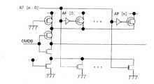
この調整は、図4に示すドライバ回路に供給する信号AF[0]〜AF[n]を用いて複数のトランジスタをON/OFFすることで可能となる。例えば、n/2のAF[*]をHigh(ON)とし、残りのn/2のAF[*]をLow(OFF)とし(後述するように、アンチヒューズは、未書き込みの状態で0出力、1出力を任意に設定可能であり、書き込みによってその0/1出力を逆転させることができる)、これを基準に、例えば、図5に示すようにMRS CMD信号から生成された内部信号(CMDB信号)が遅れている時には、図4のOFF指定しているトランジスタを書き込みによってONに変えることで、ドライブ能力を高めて内部信号の遅延量を少なくすることができる。逆にトランジスタのOFFを増やすことで内部信号の遅延量を大きくことができる。そのため、内部Latch CLK信号(CLK)に対して、tIS、tIHの調整が可能となる。この説明では、全てのトランジスタを同一サイズとしたが、各トランジスタのサイズを2のべき乗の比例して変えることでアンチヒューズの数を少なくすることも可能である。 This adjustment can be performed by turning on / off a plurality of transistors using signals AF [0] to AF [n] supplied to the driver circuit shown in FIG. For example, n / 2 AF [*] is set to High (ON), and the remaining n / 2 AF [*] is set to Low (OFF) (as will be described later, the
アンチヒューズは、上記内部信号のタイミング調整の他に、従来、不良メモリセルの救済にも用いられ、半導体記憶装置では、初期設定時に、これらのFuseデータの読み出し、及び読み出したFuseデータを用いた処理を実施する。なお、上記内部信号のタイミング調整用のFuseデータは、初期設定時に供給されるMRS CMD信号(Mode Register Set Command)に基づいて生成されるFuse読み出し信号を用いて読み出されていた。 Antifuses are conventionally used to repair defective memory cells in addition to the timing adjustment of the internal signals. In the semiconductor memory device, these Fuse data are read and the read Fuse data are used at the time of initial setting. Implement the process. Note that the Fuse data for timing adjustment of the internal signal has been read using a Fuse read signal generated based on an MRS CMD signal (Mode Register Set Command) supplied at the time of initial setting.
図6に示すように、アンチヒューズブロック1(図3参照)は、Fuse読み出し信号を保持するリセット(Reset)保持回路11と、Fuseデータが記録されたアンチヒューズ(AntiFuse)部12と、アンチヒューズ部12から出力された情報をデコードし、FuseデータAF[n:0]として出力するヒューズデコーダ部(Fuse Decode Counter)13とを有する。 As shown in FIG. 6, the antifuse block 1 (see FIG. 3) includes a
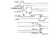
図7に示すように、アンチヒューズブロック1は、リセット保持回路11に入力されるFFRST信号によりFuse読み出し信号が受け入れ可能になる。リセット保持回路11は、Fuse読み出し信号が入力されると、該Fuse読み出し信号を保持すると共に、アンチヒューズ部12へFuseデータを出力させるためのAFLOAD信号を出力する。 As shown in FIG. 7, the antifuse block 1 can accept the Fuse read signal by the FFRST signal input to the
アンチヒューズ部12は、ヒューズ素子を挟んでドレインどうしが接続されたPチャネルMOSトランジスタ及びNチャネルMOSトランジスタから成る複数の記憶部を備え、各記憶部はヒューズ素子の状態(切断/未切断)に応じて「High」または「Low」信号を出力する。各記憶部から出力された信号はヒューズデコーダ部13によってデコードされ、FuseデータAF[n:0]として出力される。 The
アンチヒューズブロック1は、FuseデータAF[n:0]を出力するためのタイミング信号が異なることを除けば、不良メモリセルを救済するためのアンチヒューズブロックと同様の回路構成を用いればよく、図6に示した回路に限定されるものではない。 The antifuse block 1 may have a circuit configuration similar to that of the antifuse block for relieving a defective memory cell, except that the timing signal for outputting the fuse data AF [n: 0] is different. The circuit is not limited to the circuit shown in FIG.
図3は、内部信号の遅延量調整用のFuseデータを読み出すために、従来の冗長回路と同様にMRS CMD信号でFuseデータを読み出す場合のアンチヒューズ制御回路の構成を示すブロック図であり、図4は図3に示した遅延切替回路の構成例を示す回路図である。また、図5は図3に示したラッチ回路の動作を示すタイミングチャートである。図6は図3に示したアンチヒューズブロックの構成例を示す回路図であり、図7は図6に示したアンチヒューズブロックの動作を示すタイミングチャートである。 FIG. 3 is a block diagram showing a configuration of an antifuse control circuit when reading Fuse data with an MRS CMD signal in the same manner as a conventional redundant circuit in order to read Fuse data for adjusting the delay amount of the internal signal. 4 is a circuit diagram showing a configuration example of the delay switching circuit shown in FIG. FIG. 5 is a timing chart showing the operation of the latch circuit shown in FIG. 6 is a circuit diagram showing a configuration example of the antifuse block shown in FIG. 3, and FIG. 7 is a timing chart showing an operation of the antifuse block shown in FIG.
図3に示すように、従来のアンチヒューズ制御回路は、Fuseデータが記録され、該Fuseデータを遅延切替回路2へ供給するアンチヒューズブロック1と、アンチヒューズブロック1から出力されたFuseデータにしたがってMRS CMD信号から生成された内部信号(CMDB信号)の遅延量を切り替える遅延切替回路2と、遅延切替回路2から出力されたCMDB信号を検知し、クロックCLKに同期したコマンド(PMDCMDT)信号を生成するラッチ回路4と、ラッチ回路4から出力されたPMDCMDT信号を、PMRS信号及びADD2信号の値に応じてFuse読み出し信号として出力するFuse読み出し信号生成回路5とを有する。 As shown in FIG. 3, the conventional antifuse control circuit records the fuse data and supplies the fuse data to the
アンチヒューズにより内部信号の遅延量を調整する場合、ラッチ回路4の出力信号をそのまま出せば、未書き込みで「0」、書き込みで「1」が出力されるが、ラッチ回路4の出力信号を反転して出せば、未書き込みで「1」、書き込みで「0」となり、前述のドライバ回路が有するトランジスタのON/OFFが任意に設定できることがわかる。 When adjusting the delay amount of the internal signal by the antifuse, if the output signal of the latch circuit 4 is output as it is, “0” is output when not written and “1” is output when written, but the output signal of the latch circuit 4 is inverted. Thus, it can be seen that “1” is written when not written and “0” is written, so that ON / OFF of the transistor included in the driver circuit can be arbitrarily set.
CMDB信号は、初期設定時に半導体記憶装置の各種入力信号にしたがって生成されるMRS CMD信号を基に生成される。PMRS信号及びADD2信号は、Fuse読み出し信号を出力するためのゲート信号として用いられる、初期設定時に半導体記憶装置の各種入力信号にしたがって生成されるコード信号である。 The CMDB signal is generated based on the MRS CMD signal generated according to various input signals of the semiconductor memory device at the time of initial setting. The PMRS signal and the ADD2 signal are code signals used as gate signals for outputting a Fuse read signal and generated according to various input signals of the semiconductor memory device at the initial setting.
Fuse読み出し信号生成回路5から出力されたFuse読み出し信号は、複数のアンチヒューズを備えたアンチヒューズブロック1へ供給され、アンチヒューズブロック1は、Fuse読み出し信号を受けて、内部に書き込まれたFuseデータを出力する。 The Fuse read signal output from the Fuse read
図4に示すように、遅延切替回路2は、ドレインどうしが接続されたPチャネルMOSトランジスタ及びNチャネルMOSトランジスタから構成されるドライバ回路と、ドライバ回路のPチャネルMOSトランジスタに電源電圧を供給する、並列に接続された複数の調整用PチャネルMOSトランジスタと、ドライバ回路のNチャネルMOSトランジスタに接地電位を供給する、並列に接続された複数の調整用NチャネルMOSトランジスタとを有する構成である。アンチヒューズブロック1から読み出されたFuseデータAF[n:0]は、並列に接続された複数の調整用PチャネルMOSトランジスタ及び複数の調整用NチャネルMOSトランジスタに供給され、それぞれのON/OFF制御に用いられる。 As shown in FIG. 4, the
遅延切替回路2は、ドライバ回路と共に動作する調整用PチャネルMOSトランジスタ及び調整用NチャネルMOSトランジスタの数をそれぞれ変更することで、入力されたCMDB信号を所定の遅延量だけ遅延させて出力する。 The
図5に示すように、ラッチ回路4は、遅延切替回路2から出力された遅延量調整後のCMDB信号を検知し、クロックCLKに同期した、アンチヒューズブロック1からFuseデータを読み出すのに必要なコマンド信号PMDCMDT信号を出力する。このとき、ラッチ回路4でCMDB信号を検知するためには、上述したようにCMDB信号が立ち下がってからクロックCLKが立上るまでの時間であるSetup時間(tIS)及びクロックCLKが立上ってからCMDB信号が立上るまでの時間であるHold時間(tIH)をそれぞれ確保する必要がある。 As shown in FIG. 5, the latch circuit 4 detects the CMDB signal after adjusting the delay amount output from the
ラッチ回路4から出力されたPMDCMDT信号は、PMRS信号及びADD2信号がそれぞれ「High」のとき、Fuse読み出し信号生成回路5からFuse読み出し信号として出力される。 The PMDCMT signal output from the latch circuit 4 is output as a Fuse read signal from the Fuse read
先行技術文献情報なし。 There is no prior art document information.
従来、DRAM等の半導体記憶装置を初期設定する際には、電源の立ち上がりで発生させるPower−On信号(以下、PON)や初期設定のためのCMD(MRS CMD)を用いて動作させている場合が多い。しかしながら、これらの動作は不確定であり、必ず実行されるとは限らない。例えば、PON信号は、システムによる電源投入時の電圧及びその傾きなどにより動作せず、保障できない場合が考えられる。また、内部でCMD信号を発生する場合は、高い動作周波数下での厳しいtIS/tIH条件下においては、CLKとCMDのtIS/tIHにずれが発生した場合に、CMD信号が生成されず、動作しなくなる場合が考えられる。逆に言えば、タイミング調整を行ってこそ正しくコマンドを取り込むことができるのであって、未調整、あるいは電源投入時のフリップフロップがどうなっているかは不定である。そのため、内部遅延値がどう設定されているかは不明であり、正しいコマンドの取り込みが行える保証はなく、今後の高い動作周波数条件下において、これらの不確定要素から100%の動作保障をすることは難しい。 Conventionally, when a semiconductor memory device such as a DRAM is initially set, it is operated using a power-on signal (hereinafter referred to as PON) generated at power-on or a CMD (MRS CMD) for initial setting. There are many. However, these operations are indeterminate and are not always executed. For example, the PON signal may not be guaranteed because it does not operate due to the voltage when the power is turned on by the system and its inclination. In addition, when a CMD signal is generated internally, under a severe tIS / tIH condition under a high operating frequency, when a deviation occurs between tIS / tIH of CLK and CMD, the CMD signal is not generated and the operation is performed. The case where it does not do is considered. In other words, the command can be correctly fetched only by adjusting the timing, and it is undefined whether the flip-flop is unadjusted or turned on. For this reason, it is unclear how the internal delay value is set, and there is no guarantee that correct commands can be fetched. Under the future high operating frequency conditions, it is not possible to guarantee 100% operation from these uncertain factors. difficult.
上述したように従来のアンチヒューズ制御回路では、初期設定時に生成されるFuse読み出し信号によってアンチヒューズブロックからFuseデータが出力される。そのため、図8に示すように、初期設定時にクロックCLKとCMDB信号の位相関係がずれていると、上記tIS/tIHの仕様値を確保できずにラッチ回路からPMDCMDT信号が出力されず、Fuse読み出し信号が生成されないおそれがある。 As described above, in the conventional antifuse control circuit, the fuse data is output from the antifuse block by the fuse read signal generated at the time of initial setting. Therefore, as shown in FIG. 8, if the phase relationship between the clock CLK and the CMDB signal is deviated at the time of initial setting, the specification value of the tIS / tIH cannot be ensured, and the PMDCMT signal is not output from the latch circuit, and the Fuse read-out is performed. The signal may not be generated.
その場合、アンチヒューズブロックからFuseデータが出力されないため、遅延量切替回路にてCMDB信号の遅延量が切り替わることもなく、半導体記憶装置が正常に動作しなくなってしまう。 In that case, since the fuse data is not output from the antifuse block, the delay amount of the CMDB signal is not switched by the delay amount switching circuit, and the semiconductor memory device does not operate normally.
また、Fuse読み出し信号が生成されなければ、半導体記憶装置の組み立て後に実施する、アンチヒューズにFuseデータを書き込むための調整試験(上記内部信号のタイミング調整)が不能となる。 If the Fuse read signal is not generated, the adjustment test (timing adjustment of the internal signal) for writing the Fuse data to the antifuse, which is performed after the assembly of the semiconductor memory device, becomes impossible.
特に、より高いクロック周波数で動作することが予想される今後の半導体記憶装置では、上記tIS/tIHに対する規定も益々厳しくなり、上記のような不確定要素から半導体記憶装置の正常動作を保障することがより困難になる。 In particular, in future semiconductor memory devices that are expected to operate at a higher clock frequency, the regulations for the tIS / tIH are becoming more stringent, and the normal operation of the semiconductor memory device is ensured from the above uncertain factors. Becomes more difficult.
本発明は上記したような従来の技術が有する問題点を解決するためになされたものであり、初期設定時にアンチヒューズに書き込まれたデータが確実に得られるようにして内部信号のタイミング調整を実施できる半導体記憶装置及びその調整方法を提供することを目的とする。 The present invention has been made to solve the above-described problems of the prior art, and the timing of the internal signal is adjusted so that the data written in the antifuse can be reliably obtained at the initial setting. An object of the present invention is to provide a semiconductor memory device and a method for adjusting the same.
上記目的を達成するため本発明の半導体記憶装置は、初期設定時に生成される内部信号のタイミング調整に必要なデータが書き込まれる複数のアンチヒューズを備えたアンチヒューズブロックと、
前記データにしたがって前記内部信号を所定の遅延量で遅延させる遅延量切替回路と、
前記遅延量切替回路から出力される前記遅延後の内部信号を基に、前記アンチヒューズブロックから前記データを読み出すのに必要なコマンド信号を生成するラッチ回路と、
前記コマンド信号及びクロックと非同期に供給されるリセット信号を用いて生成する、前記アンチヒューズから前記データを出力させるための信号であるDLLReset信号を前記アンチヒューズブロックへ供給するDLLリセット信号生成回路と、
を有する。In order to achieve the above object, a semiconductor memory device of the present invention includes an antifuse block including a plurality of antifuses to which data necessary for timing adjustment of an internal signal generated at initial setting is written,
A delay amount switching circuit for delaying the internal signal by a predetermined delay amount according to the data;
Based on the delayed internal signal output from the delay amount switching circuit, a latch circuit that generates a command signal necessary for reading the data from the antifuse block;
A DLL reset signal generation circuit for generating a DLL Reset signal, which is a signal for outputting the data from the antifuse, generated using a reset signal supplied asynchronously with the command signal and the clock;
Have
一方、本発明の半導体記憶装置の調整方法は、初期設定時にアンチヒューズに書き込まれたデータを用いて内部信号のタイミング調整を実施する半導体記憶装置の調整方法であって、
クロックと非同期に供給されるリセット信号を用いて前記アンチヒューズから前記データを出力させるための信号であるDLLReset信号を生成し、
前記DLLReset信号を、前記内部信号のタイミング調整に必要なデータが書き込まれた複数のアンチヒューズを備えたアンチヒューズブロックへ供給する方法である。On the other hand, the semiconductor memory device adjustment method of the present invention is a semiconductor memory device adjustment method that performs internal signal timing adjustment using data written to the antifuse during initial setting,
A DLL Reset signal, which is a signal for outputting the data from the antifuse, is generated using a reset signal supplied asynchronously with a clock,
The DLL Reset signal is supplied to an anti-fuse block including a plurality of anti-fuses in which data necessary for timing adjustment of the internal signal is written.
上記のような半導体記憶装置では、クロックと非同期に供給されるリセット信号を用いてアンチヒューズからデータを出力させるための信号であるDLLReset信号を生成するため、クロック周波数が高くてもDLLReset信号を確実に生成され、アンチヒューズに書き込まれたデータが確実に出力される。 In the semiconductor memory device as described above, the DLL Reset signal, which is a signal for outputting data from the antifuse, is generated using the reset signal supplied asynchronously with the clock, so that the DLL Reset signal is surely generated even when the clock frequency is high. The data generated and written to the antifuse is reliably output.
本発明によれば、アンチヒューズからデータを出力させるためのDLLReset信号が確実に生成されるため、内部信号の遅延量をアンチヒューズに書き込まれたデータによって所望の値に確実に切り替えることが可能になり、ラッチ回路からコマンド信号が確実に出力される。よって、半導体記憶装置の組み立て後に実施する、アンチヒューズにデータを書き込むための調整試験(内部信号のタイミング調整)を確実に実施できる。 According to the present invention, since the DLL Reset signal for outputting data from the antifuse is reliably generated, the delay amount of the internal signal can be reliably switched to a desired value by the data written in the antifuse. Thus, the command signal is reliably output from the latch circuit. Therefore, it is possible to reliably perform an adjustment test (timing adjustment of internal signals) for writing data to the antifuse, which is performed after the assembly of the semiconductor memory device.
また、より高いクロック周波数で動作することが予想される今後の半導体記憶装置であっても、アンチヒューズに書き込まれたデータを確実に得ることができるため、クロックに対する内部信号のtIS/tIHの仕様値を満たす半導体記憶装置が得られる。そのため、半導体記憶装置の製造上の歩留りが向上する。 Further, even in a future semiconductor memory device expected to operate at a higher clock frequency, the data written in the antifuse can be obtained with certainty, so the specification of tIS / tIH of the internal signal with respect to the clock A semiconductor memory device satisfying the values can be obtained. Therefore, the manufacturing yield of the semiconductor memory device is improved.
次に本発明について図面を参照して説明する。 Next, the present invention will be described with reference to the drawings.
図1は本発明のアンチヒューズ制御回路の一構成例を示す回路図であり、図2は本発明のアンチヒューズ制御回路が有するラッチ回路の動作を示すタイミングチャートである。 FIG. 1 is a circuit diagram showing a configuration example of the antifuse control circuit of the present invention, and FIG. 2 is a timing chart showing the operation of the latch circuit included in the antifuse control circuit of the present invention.
図1に示すように、本発明のアンチヒューズ制御回路は、Fuse読み出し信号生成回路5に代えてDLLリセット信号生成回路を用いている点が図3に示した従来のアンチヒューズ制御回路と異なっている。その他の構成及び動作は従来のアンチヒューズ回路と同様であるため、その説明は省略する。 As shown in FIG. 1, the antifuse control circuit of the present invention is different from the conventional antifuse control circuit shown in FIG. 3 in that a DLL reset signal generation circuit is used instead of the Fuse read
図1に示すように、本発明のアンチヒューズ制御回路が有するDLLリセット信号生成回路6は、従来のFuse読み出し信号生成回路5と同様に、ラッチ回路から出力されたPMDCMDT信号に基づきDLLReset信号を出力する。このとき、コード信号であるPMRS信号及びADD2信号の値に応じてDLLReset信号の出力/非出力を制御する。 As shown in FIG. 1, the DLL reset signal generation circuit 6 included in the antifuse control circuit according to the present invention outputs a DLL Reset signal based on the PMDCMT signal output from the latch circuit, similarly to the conventional Fuse read
さらに、本発明のアンチヒューズ制御回路が有するDLLリセット信号生成回路6では、DDR3−SDRAMにて採用された、システムのPower−OnからMRS CMD信号が生成されるまでの期間(初期設定期間)に外部から供給される、クロックCLKと非同期なRESET信号が入力された場合もDLLReset信号を生成して出力する。 Further, in the DLL reset signal generation circuit 6 included in the antifuse control circuit of the present invention, the period (initial setting period) until the MRS CMD signal is generated from the power-on of the system adopted in the DDR3-SDRAM. A DLL Reset signal is also generated and output when a RESET signal that is supplied externally and asynchronous with the clock CLK is input.
このようにクロックCLKと非同期なRESET信号を用いてDLLReset信号を生成することで、クロック周波数が高くてもDLLReset信号を確実に生成できるため、アンチヒューズブロックから確実にFuseデータが出力される。したがって、図2に示すように、CMDB信号の遅延量をFuseデータによって所望の値に確実に切り替えることが可能になり、ラッチ回路からPMDCMDT信号が確実に出力される。 By generating the DLL Reset signal using the RESET signal asynchronous with the clock CLK in this way, the DLL Reset signal can be generated reliably even when the clock frequency is high, so that the Fuse data is reliably output from the antifuse block. Therefore, as shown in FIG. 2, the delay amount of the CMDB signal can be reliably switched to a desired value by the Fuse data, and the PMDCMT signal is reliably output from the latch circuit.
この遅延量の調整例について図9を用いて説明する。 An example of adjusting the delay amount will be described with reference to FIG.
図9は図1に示したアンチヒューズブロック1の回路例を示している。図9に示すアンチヒューズ(AutiFuse)部12は、TestCode信号で動作するClked Inverterを用い、テストモード時にアンチヒューズ部12の記憶部に1/0をセットすることにより、任意のデータを擬似的に記憶部にラッチさせ、プログラマブルにてヒューズを切ることなく図4に示したトランジスタのON/OFFを設定可能にしている。このようにTestCode信号を用い、強制的に調整量を入力することで遅延量を変化させることができる。その設定は実使用の高速条件下ではなく、tIS/tIHが比較的緩い低速条件下にて擬似的にTestCodeにてAF[*]を入力し、これを回路内にてラッチさせ、高速条件下にて動作確認を行い、調整量を可変させることで高速条件下での動作状態を見出すことが可能となる。 FIG. 9 shows a circuit example of the antifuse block 1 shown in FIG. The anti-fuse (AutiFuse)
よって、半導体記憶装置の組み立て後に実施する、アンチヒューズにFuseデータを書き込むための調整試験(内部信号のタイミング調整)を確実に実施できる。 Therefore, it is possible to reliably perform the adjustment test (timing adjustment of internal signals) for writing the fuse data into the antifuse, which is performed after the assembly of the semiconductor memory device.
また、より高いクロック周波数で動作することが予想される今後の半導体記憶装置であっても、アンチヒューズブロックに書き込まれたFuseデータを確実に得ることができるため、クロックCLKに対する内部信号のtIS/tIHの仕様値を満たす半導体記憶装置が得られる。そのため、半導体記憶装置の製造上の歩留りが向上する。 Further, even in a future semiconductor memory device that is expected to operate at a higher clock frequency, the Fuse data written in the antifuse block can be reliably obtained. A semiconductor memory device that satisfies the specification value of tIH is obtained. Therefore, the manufacturing yield of the semiconductor memory device is improved.
本発明では、半導体記憶装置を例にして、図1に示したように、MRS信号もしくはCLKと非同期なリセット信号からの双方によってDLL−Reset信号を生成可能とし、確実に自己回路内の遅延量の調整を可能としているが、このリセット信号を利用したFuse読み出しによる自己回路内の遅延量調整については、半導体記憶装置だけではなく、一般的な半導体装置にも応用可能であることは簡単に推測できる。 In the present invention, taking a semiconductor memory device as an example, as shown in FIG. 1, a DLL-Reset signal can be generated by both an MRS signal or a reset signal asynchronous with CLK, and the delay amount in the self-circuit is surely generated. Although it is possible to adjust the delay amount in the self circuit by Fuse reading using this reset signal, it is easily assumed that it can be applied not only to a semiconductor memory device but also to a general semiconductor device. it can.
なお、RESET信号を用いて初期設定を行う例としては、CPUのパワーオンリセットが考えられる。しかしながら、CPUは、リセット信号と称するSTART信号によりROM等に格納されたプログラムを読み出し、周辺機器の初期設定に必要なデータを読み出す動作である。したがって、本発明のようにリセット信号を半導体装置内部のタイミング調整に用いるものではない。 As an example of performing the initial setting using the RESET signal, a power-on reset of the CPU can be considered. However, the CPU reads out a program stored in a ROM or the like by a START signal called a reset signal, and reads out data necessary for initial setting of peripheral devices. Therefore, unlike the present invention, the reset signal is not used for timing adjustment inside the semiconductor device.
1 アンチヒューズブロック
2 遅延切替回路
4 ラッチ回路
5 Fuse読み出し信号生成回路
6 DLLリセット信号生成回路
11 リセット保持回路
12 アンチヒューズ部
13 ヒューズデコーダ部DESCRIPTION OF SYMBOLS 1
Claims (3)
Translated fromJapanese前記データにしたがって前記内部信号を所定の遅延量で遅延させる遅延量切替回路と、
前記遅延量切替回路から出力される前記遅延後の内部信号を基に、前記アンチヒューズブロックから前記データを読み出すのに必要なコマンド信号を生成するラッチ回路と、
前記コマンド信号及びクロックと非同期に供給されるリセット信号を用いて生成する、前記アンチヒューズから前記データを出力させるための信号であるDLLReset信号を前記アンチヒューズブロックへ供給するDLLリセット信号生成回路と、
を有する半導体記憶装置。An anti-fuse block having a plurality of anti-fuses to which data necessary for timing adjustment of internal signals generated at the initial setting is written;
A delay amount switching circuit for delaying the internal signal by a predetermined delay amount according to the data;
Based on the delayed internal signal output from the delay amount switching circuit, a latch circuit that generates a command signal necessary for reading the data from the antifuse block;
A DLL reset signal generation circuit for generating a DLL Reset signal, which is a signal for outputting the data from the antifuse, generated using a reset signal supplied asynchronously with the command signal and the clock;
A semiconductor memory device.
クロックと非同期に供給されるリセット信号を用いて前記アンチヒューズから前記データを出力させるための信号であるDLLReset信号を生成し、
前記DLLReset信号を、前記内部信号のタイミング調整に必要なデータが書き込まれた複数のアンチヒューズを備えたアンチヒューズブロックへ供給する半導体記憶装置の調整方法。A method of adjusting a semiconductor memory device that performs timing adjustment of an internal signal using data written to an antifuse at the time of initial setting,
A DLL Reset signal, which is a signal for outputting the data from the antifuse, is generated using a reset signal supplied asynchronously with a clock,
A method of adjusting a semiconductor memory device, wherein the DLL Reset signal is supplied to an anti-fuse block having a plurality of anti-fuses in which data necessary for timing adjustment of the internal signal is written.
前記半導体装置の内部で生成されるコマンド信号及びクロック信号と非同期に供給されるリセット信号を用いて、自回路内に設けられた前記アンチヒューズに書き込まれたデータを読み込み、
前記内部信号のタイミング調整を行う半導体装置の調整方法。A method of adjusting a semiconductor device for performing timing adjustment of an internal signal using data written in an antifuse at the time of initial setting,
Using the reset signal supplied asynchronously with the command signal and the clock signal generated inside the semiconductor device, the data written in the antifuse provided in its own circuit is read,
A method of adjusting a semiconductor device for adjusting the timing of the internal signal.
Priority Applications (2)
| Application Number | Priority Date | Filing Date | Title |
|---|---|---|---|
| JP2005313387AJP2007122807A (en) | 2005-10-27 | 2005-10-27 | Semiconductor storage device and its adjustment method |
| US11/585,948US7411852B2 (en) | 2005-10-27 | 2006-10-25 | Semiconductor memory device and method of adjusting same |
Applications Claiming Priority (1)
| Application Number | Priority Date | Filing Date | Title |
|---|---|---|---|
| JP2005313387AJP2007122807A (en) | 2005-10-27 | 2005-10-27 | Semiconductor storage device and its adjustment method |
Publications (1)
| Publication Number | Publication Date |
|---|---|
| JP2007122807Atrue JP2007122807A (en) | 2007-05-17 |
Family
ID=37996096
Family Applications (1)
| Application Number | Title | Priority Date | Filing Date |
|---|---|---|---|
| JP2005313387APendingJP2007122807A (en) | 2005-10-27 | 2005-10-27 | Semiconductor storage device and its adjustment method |
Country Status (2)
| Country | Link |
|---|---|
| US (1) | US7411852B2 (en) |
| JP (1) | JP2007122807A (en) |
Cited By (3)
| Publication number | Priority date | Publication date | Assignee | Title |
|---|---|---|---|---|
| US8593897B2 (en) | 2010-02-17 | 2013-11-26 | Elpida Memory, Inc. | Memory controller, semiconductor storage device, and memory system including the memory controller and the semiconductor storage device for outputting temperature value in low power consumption mode |
| CN105378561A (en)* | 2013-08-05 | 2016-03-02 | 精工爱普生株式会社 | Illumination device and projector |
| CN110995215A (en)* | 2019-12-16 | 2020-04-10 | 北京时代民芯科技有限公司 | Gain-adjustable high-speed high-precision comparator circuit |
Families Citing this family (28)
| Publication number | Priority date | Publication date | Assignee | Title |
|---|---|---|---|---|
| US7716510B2 (en) | 2006-12-19 | 2010-05-11 | Micron Technology, Inc. | Timing synchronization circuit with loop counter |
| US7656745B2 (en) | 2007-03-15 | 2010-02-02 | Micron Technology, Inc. | Circuit, system and method for controlling read latency |
| TWI393145B (en)* | 2007-10-29 | 2013-04-11 | Elpida Memory Inc | Semiconductor device including anti-fuse circuit, and method of writing address to anti-fuse circuit |
| KR20090098295A (en)* | 2008-03-13 | 2009-09-17 | 주식회사 하이닉스반도체 | Input latch circuit |
| KR101022669B1 (en)* | 2008-12-02 | 2011-03-22 | 주식회사 하이닉스반도체 | Delay fixed loop circuit |
| US7969813B2 (en) | 2009-04-01 | 2011-06-28 | Micron Technology, Inc. | Write command and write data timing circuit and methods for timing the same |
| CN101813966B (en)* | 2010-04-02 | 2012-02-29 | 华为技术有限公司 | A chip reset method, chip and double-rate memory system |
| US8984320B2 (en) | 2011-03-29 | 2015-03-17 | Micron Technology, Inc. | Command paths, apparatuses and methods for providing a command to a data block |
| US8717835B2 (en) | 2011-08-23 | 2014-05-06 | Micron Technology, Inc. | Apparatuses and methods for compensating for power supply sensitivities of a circuit in a clock path |
| US8552776B2 (en) | 2012-02-01 | 2013-10-08 | Micron Technology, Inc. | Apparatuses and methods for altering a forward path delay of a signal path |
| KR101953241B1 (en)* | 2012-05-02 | 2019-02-28 | 삼성전자 주식회사 | Anti-fuse circuit capable of monitoring anti-fuse cell data, and semiconductor device including the same |
| US9166579B2 (en) | 2012-06-01 | 2015-10-20 | Micron Technology, Inc. | Methods and apparatuses for shifting data signals to match command signal delay |
| US9054675B2 (en) | 2012-06-22 | 2015-06-09 | Micron Technology, Inc. | Apparatuses and methods for adjusting a minimum forward path delay of a signal path |
| US9329623B2 (en) | 2012-08-22 | 2016-05-03 | Micron Technology, Inc. | Apparatuses, integrated circuits, and methods for synchronizing data signals with a command signal |
| US8913448B2 (en) | 2012-10-25 | 2014-12-16 | Micron Technology, Inc. | Apparatuses and methods for capturing data in a memory |
| US9734097B2 (en) | 2013-03-15 | 2017-08-15 | Micron Technology, Inc. | Apparatuses and methods for variable latency memory operations |
| US9727493B2 (en) | 2013-08-14 | 2017-08-08 | Micron Technology, Inc. | Apparatuses and methods for providing data to a configurable storage area |
| US9071235B2 (en) | 2013-10-18 | 2015-06-30 | Micron Technology, Inc. | Apparatuses and methods for changing signal path delay of a signal path responsive to changes in power |
| US9183904B2 (en) | 2014-02-07 | 2015-11-10 | Micron Technology, Inc. | Apparatuses, memories, and methods for facilitating splitting of internal commands using a shared signal path |
| US9508417B2 (en) | 2014-02-20 | 2016-11-29 | Micron Technology, Inc. | Methods and apparatuses for controlling timing paths and latency based on a loop delay |
| US9530473B2 (en) | 2014-05-22 | 2016-12-27 | Micron Technology, Inc. | Apparatuses and methods for timing provision of a command to input circuitry |
| US9698766B2 (en) | 2014-12-03 | 2017-07-04 | Micron Technology, Inc. | Apparatuses and methods for adjusting timing of signals |
| US9531363B2 (en) | 2015-04-28 | 2016-12-27 | Micron Technology, Inc. | Methods and apparatuses including command latency control circuit |
| US9813067B2 (en) | 2015-06-10 | 2017-11-07 | Micron Technology, Inc. | Clock signal and supply voltage variation tracking |
| US9601170B1 (en) | 2016-04-26 | 2017-03-21 | Micron Technology, Inc. | Apparatuses and methods for adjusting a delay of a command signal path |
| US9865317B2 (en) | 2016-04-26 | 2018-01-09 | Micron Technology, Inc. | Methods and apparatuses including command delay adjustment circuit |
| US9997220B2 (en) | 2016-08-22 | 2018-06-12 | Micron Technology, Inc. | Apparatuses and methods for adjusting delay of command signal path |
| US10224938B2 (en) | 2017-07-26 | 2019-03-05 | Micron Technology, Inc. | Apparatuses and methods for indirectly detecting phase variations |
Citations (4)
| Publication number | Priority date | Publication date | Assignee | Title |
|---|---|---|---|---|
| JP2000311496A (en)* | 1999-04-28 | 2000-11-07 | Nec Corp | Redundant address setting circuit and semiconductor memory incorporating the circuit |
| JP2002064373A (en)* | 1999-07-23 | 2002-02-28 | Seiko Epson Corp | Semiconductor integrated circuit, liquid crystal device, electronic device, and method of inspecting semiconductor integrated circuit |
| JP2003007082A (en)* | 2001-06-19 | 2003-01-10 | Hitachi Ltd | Semiconductor device |
| JP2005116151A (en)* | 2003-09-16 | 2005-04-28 | Toshiba Corp | Semiconductor memory device |
Family Cites Families (5)
| Publication number | Priority date | Publication date | Assignee | Title |
|---|---|---|---|---|
| US5946244A (en)* | 1997-03-05 | 1999-08-31 | Micron Technology, Inc. | Delay-locked loop with binary-coupled capacitor |
| KR100513806B1 (en)* | 2000-12-30 | 2005-09-13 | 주식회사 하이닉스반도체 | Semiconductor Device |
| JP2002230972A (en)* | 2001-02-06 | 2002-08-16 | Mitsubishi Electric Corp | Synchronous semiconductor memory |
| US7111185B2 (en)* | 2003-12-23 | 2006-09-19 | Micron Technology, Inc. | Synchronization device with delay line control circuit to control amount of delay added to input signal and tuning elements to receive signal form delay circuit |
| US7106099B1 (en)* | 2004-10-22 | 2006-09-12 | Xilinx, Inc. | Decision-feedback equalization clocking apparatus and method |
- 2005
- 2005-10-27JPJP2005313387Apatent/JP2007122807A/enactivePending
- 2006
- 2006-10-25USUS11/585,948patent/US7411852B2/ennot_activeExpired - Fee Related
Patent Citations (4)
| Publication number | Priority date | Publication date | Assignee | Title |
|---|---|---|---|---|
| JP2000311496A (en)* | 1999-04-28 | 2000-11-07 | Nec Corp | Redundant address setting circuit and semiconductor memory incorporating the circuit |
| JP2002064373A (en)* | 1999-07-23 | 2002-02-28 | Seiko Epson Corp | Semiconductor integrated circuit, liquid crystal device, electronic device, and method of inspecting semiconductor integrated circuit |
| JP2003007082A (en)* | 2001-06-19 | 2003-01-10 | Hitachi Ltd | Semiconductor device |
| JP2005116151A (en)* | 2003-09-16 | 2005-04-28 | Toshiba Corp | Semiconductor memory device |
Cited By (4)
| Publication number | Priority date | Publication date | Assignee | Title |
|---|---|---|---|---|
| US8593897B2 (en) | 2010-02-17 | 2013-11-26 | Elpida Memory, Inc. | Memory controller, semiconductor storage device, and memory system including the memory controller and the semiconductor storage device for outputting temperature value in low power consumption mode |
| CN105378561A (en)* | 2013-08-05 | 2016-03-02 | 精工爱普生株式会社 | Illumination device and projector |
| CN110995215A (en)* | 2019-12-16 | 2020-04-10 | 北京时代民芯科技有限公司 | Gain-adjustable high-speed high-precision comparator circuit |
| CN110995215B (en)* | 2019-12-16 | 2023-08-29 | 北京时代民芯科技有限公司 | Gain-adjustable high-speed high-precision comparator circuit |
Also Published As
| Publication number | Publication date |
|---|---|
| US20070097773A1 (en) | 2007-05-03 |
| US7411852B2 (en) | 2008-08-12 |
Similar Documents
| Publication | Publication Date | Title |
|---|---|---|
| JP2007122807A (en) | Semiconductor storage device and its adjustment method | |
| KR101040242B1 (en) | Data strobe signal generator and semiconductor memory device using same | |
| JP4511767B2 (en) | Semiconductor memory and driving method thereof | |
| USRE44218E1 (en) | Semiconductor memory device for controlling write recovery time | |
| KR100527399B1 (en) | A DLL driver in Semiconductor Memory Device | |
| EP3379538B1 (en) | Embedded memory with setup-hold time controlled internally or externally and associated integrated circuit | |
| JP4025488B2 (en) | Semiconductor integrated circuit and control method thereof | |
| JP2012252733A (en) | Semiconductor device | |
| JPH09231767A (en) | Static semiconductor memory device | |
| KR101996003B1 (en) | Clock control device | |
| US6636443B2 (en) | Semiconductor memory device having row buffers | |
| JP4323009B2 (en) | Semiconductor device | |
| US6233183B1 (en) | Semiconductor memory device with high data access speed | |
| US7230466B2 (en) | Data strobe signal generating circuit and data strobe signal generating method | |
| US6757852B1 (en) | Self resetting high speed redundancy circuit and method thereof | |
| JP3910002B2 (en) | Semiconductor integrated circuit | |
| US7596051B2 (en) | Semiconductor memory integrated circuit | |
| US20090097330A1 (en) | Fuse latch circuit and fuse latch method | |
| US11823735B2 (en) | Semiconductor device | |
| JP4276112B2 (en) | Semiconductor device including delay locked loop circuit, delay locked loop control circuit, and method for controlling delay locked loop circuit | |
| KR100557572B1 (en) | Data refresh input device prevents power consumption | |
| JP2009163865A (en) | Input circuit of semiconductor storage device and control method thereof | |
| US20070080722A1 (en) | Buffer | |
| KR100672135B1 (en) | Auto precharge control circuit of semiconductor memory device that generates stable auto precharge signal regardless of frequency change of external clock signal | |
| JP4751441B2 (en) | Semiconductor device |
Legal Events
| Date | Code | Title | Description |
|---|---|---|---|
| A621 | Written request for application examination | Free format text:JAPANESE INTERMEDIATE CODE: A621 Effective date:20080814 | |
| A977 | Report on retrieval | Free format text:JAPANESE INTERMEDIATE CODE: A971007 Effective date:20110630 | |
| A131 | Notification of reasons for refusal | Free format text:JAPANESE INTERMEDIATE CODE: A131 Effective date:20110727 | |
| A02 | Decision of refusal | Free format text:JAPANESE INTERMEDIATE CODE: A02 Effective date:20111122 |