JP2007122600A - Integrated circuit chip and RFID system - Google Patents
Integrated circuit chip and RFID systemDownload PDFInfo
- Publication number
- JP2007122600A JP2007122600AJP2005316806AJP2005316806AJP2007122600AJP 2007122600 AJP2007122600 AJP 2007122600AJP 2005316806 AJP2005316806 AJP 2005316806AJP 2005316806 AJP2005316806 AJP 2005316806AJP 2007122600 AJP2007122600 AJP 2007122600A
- Authority
- JP
- Japan
- Prior art keywords
- circuit
- data
- sensor
- nonvolatile memory
- voltage
- Prior art date
- Legal status (The legal status is an assumption and is not a legal conclusion. Google has not performed a legal analysis and makes no representation as to the accuracy of the status listed.)
- Pending
Links
Images


Classifications
- G—PHYSICS
- G06—COMPUTING OR CALCULATING; COUNTING
- G06K—GRAPHICAL DATA READING; PRESENTATION OF DATA; RECORD CARRIERS; HANDLING RECORD CARRIERS
- G06K19/00—Record carriers for use with machines and with at least a part designed to carry digital markings
- G06K19/06—Record carriers for use with machines and with at least a part designed to carry digital markings characterised by the kind of the digital marking, e.g. shape, nature, code
- G06K19/067—Record carriers with conductive marks, printed circuits or semiconductor circuit elements, e.g. credit or identity cards also with resonating or responding marks without active components
- G06K19/07—Record carriers with conductive marks, printed circuits or semiconductor circuit elements, e.g. credit or identity cards also with resonating or responding marks without active components with integrated circuit chips
- G06K19/0723—Record carriers with conductive marks, printed circuits or semiconductor circuit elements, e.g. credit or identity cards also with resonating or responding marks without active components with integrated circuit chips the record carrier comprising an arrangement for non-contact communication, e.g. wireless communication circuits on transponder cards, non-contact smart cards or RFIDs
- G—PHYSICS
- G06—COMPUTING OR CALCULATING; COUNTING
- G06K—GRAPHICAL DATA READING; PRESENTATION OF DATA; RECORD CARRIERS; HANDLING RECORD CARRIERS
- G06K19/00—Record carriers for use with machines and with at least a part designed to carry digital markings
- G06K19/06—Record carriers for use with machines and with at least a part designed to carry digital markings characterised by the kind of the digital marking, e.g. shape, nature, code
- G06K19/067—Record carriers with conductive marks, printed circuits or semiconductor circuit elements, e.g. credit or identity cards also with resonating or responding marks without active components
- G06K19/07—Record carriers with conductive marks, printed circuits or semiconductor circuit elements, e.g. credit or identity cards also with resonating or responding marks without active components with integrated circuit chips
- G06K19/0716—Record carriers with conductive marks, printed circuits or semiconductor circuit elements, e.g. credit or identity cards also with resonating or responding marks without active components with integrated circuit chips at least one of the integrated circuit chips comprising a sensor or an interface to a sensor
- G06K19/0717—Record carriers with conductive marks, printed circuits or semiconductor circuit elements, e.g. credit or identity cards also with resonating or responding marks without active components with integrated circuit chips at least one of the integrated circuit chips comprising a sensor or an interface to a sensor the sensor being capable of sensing environmental conditions such as temperature history or pressure
Landscapes
- Engineering & Computer Science (AREA)
- Computer Hardware Design (AREA)
- Microelectronics & Electronic Packaging (AREA)
- Physics & Mathematics (AREA)
- General Physics & Mathematics (AREA)
- Theoretical Computer Science (AREA)
- Computer Networks & Wireless Communication (AREA)
- Near-Field Transmission Systems (AREA)
- Arrangements For Transmission Of Measured Signals (AREA)
Abstract
Translated fromJapaneseDescription
Translated fromJapanese本発明は、一般に集積回路チップに関し、詳しくはRFID用の集積回路チップ及びRFIDシステムに関する。 The present invention relates generally to integrated circuit chips, and more particularly to integrated circuit chips and RFID systems for RFID.
RFID(Radio Frequency Identification)は、情報を記録する記録媒体として機能するICチップ(集積回路チップ)を備えたICタグに対して、無線通信を介してID情報を読み書きするシステムである。例えば物品管理に利用されているバーコード等をRFIDに置き換えれば、人手によるバーコード等の読み取り作業が不要になり、物品管理の効率を飛躍的に向上させることができる。 RFID (Radio Frequency Identification) is a system that reads and writes ID information via wireless communication with an IC tag including an IC chip (integrated circuit chip) that functions as a recording medium for recording information. For example, if a barcode or the like used for article management is replaced with RFID, manual barcode reading or the like becomes unnecessary, and the efficiency of article management can be dramatically improved.
またRFIDは、物品を識別する目的以外への様々な分野への応用が期待されている。特に、ICタグが置かれている環境の状態を計測するセンサ機能を追加したRFIDは、物品の製造過程(生産過程)の履歴の記録、流通過程での管理状態の履歴の記録等にも利用することができる。 Further, RFID is expected to be applied to various fields other than for the purpose of identifying articles. In particular, RFID with a sensor function that measures the state of the environment where the IC tag is placed can also be used to record the history of the manufacturing process (production process) of an article and the history of the management status during the distribution process. can do.
例えば、生鮮食料品等に温度センサ付のRFIDタグを付けて、流通過程や加工過程における温度変化の履歴を記録すれば、鮮度・品質をきめ細かく管理することが可能となる。これにより、商品の品質劣化等の問題を改善することが可能となり、安全で品質の高い商品を提供することができる。このようにRFIDに組み込まれるセンサの種類は、温度センサに限らず、3軸センサ、圧力センサ、加速度センサ等が考えられる。 For example, if an RFID tag with a temperature sensor is attached to a fresh food product and a history of temperature changes in the distribution process or processing process is recorded, the freshness and quality can be finely managed. This makes it possible to improve problems such as product quality degradation and provide safe and high-quality products. As described above, the type of sensor incorporated in the RFID is not limited to a temperature sensor, and a triaxial sensor, a pressure sensor, an acceleration sensor, and the like are conceivable.
このようなセンサ付きRFIDを実現するためには、既存のRFID機能にセンサ機能や測定データ処理機能等を含めた回路を、1チップで実現する必要がある。しかし、ひとつのチップにRFID機能とセンサ機能とを実装するためには、高度なアナログ・デジタル混載技術が必要になるとともに、消費電力の問題を解決する必要がある。 In order to realize such an RFID with a sensor, it is necessary to realize a circuit including a sensor function and a measurement data processing function in an existing RFID function on a single chip. However, in order to mount the RFID function and the sensor function on one chip, it is necessary to have a sophisticated analog / digital mixed technology and to solve the problem of power consumption.
RFIDの性能は一般に、通信速度及び通信距離等で表される。通信速度については、標準化により一定の通信速度を実現することが要求されるので、通信距離の違いがRFID用チップの性能差として現れる。通信距離を大きくするためにRFID用チップに要求されることは、可能な限りチップ内部での消費電力を小さくすることである。 RFID performance is generally represented by communication speed, communication distance, and the like. As for the communication speed, it is required to realize a constant communication speed by standardization, so that a difference in communication distance appears as a difference in performance of the RFID chip. What is required of an RFID chip in order to increase the communication distance is to reduce power consumption inside the chip as much as possible.
ICタグには、内蔵バッテリーを電力源として動作する能動型と、バッテリーを有さずに外部から供給される磁界や電界を電力源として動作する受動型とがある。受動型は、長距離の通信には適さないが、バッテリーを有さない分だけ小型で低価格な構成とすることができる。 IC tags include an active type that operates using a built-in battery as a power source, and a passive type that operates using a magnetic field or electric field supplied from the outside without a battery as a power source. The passive type is not suitable for long-distance communication, but can be configured to be small and low-priced as long as it does not have a battery.
受動型のRFIDチップでは、外部のリーダ・ライタから発信される電磁波を受信して電力に変換し、チップ内部のキャパシタに電力を蓄えてチップ動作用電源として使用する。従って、チップ内部での消費電力が小さいほど、受信する電磁波電力は小さくてよく、長い通信距離を実現することができる。センサ機能付のRFID用チップの場合には、RFID機能用の回路に加えて更にセンサ機能用の回路が電力を消費するので、所望の通信距離を維持することが困難となる。
以上を鑑みて、本発明は、通信距離を落とすことなくセンサ機能を動作させることが可能なRFID用のICチップ及びRFIDシステムを提供することを目的とする。 In view of the above, an object of the present invention is to provide an RFID IC chip and an RFID system that can operate a sensor function without reducing the communication distance.
本発明による集積回路チップは、アンテナに結合され該アンテナからの交流電圧を直流電圧に変換するよう機能する整流回路と、該整流回路に結合され該直流電圧で動作する不揮発性メモリと、該整流回路に結合され該直流電圧で動作し所定のデータを測定するセンサ回路と、該不揮発性メモリのアクセス動作と該センサ回路のデータ測定動作とが同時に実行されないように該不揮発性メモリと該センサ回路とを制御するロジック回路を含むことを特徴とする。 An integrated circuit chip according to the present invention includes a rectifier circuit that is coupled to an antenna and functions to convert an AC voltage from the antenna into a DC voltage, a nonvolatile memory that is coupled to the rectifier circuit and operates at the DC voltage, and the rectifier A sensor circuit coupled to a circuit and operating at the DC voltage to measure predetermined data; and the nonvolatile memory and the sensor circuit so that an access operation of the nonvolatile memory and a data measurement operation of the sensor circuit are not performed simultaneously. And a logic circuit for controlling the above.
本発明によるRFIDシステムは、電波を送受信するリーダ・ライタと、該リーダ・ライタと該電波を介して通信するICタグを含み、該ICタグは、アンテナと、該アンテナに結合され該アンテナが受信した該電波の交流電圧を直流電圧に変換するよう機能する整流回路と、該整流回路に結合され該直流電圧で動作する不揮発性メモリと、該整流回路に結合され該直流電圧で動作し所定のデータを測定するセンサ回路を含み、該不揮発性メモリのアクセス動作と該センサ回路のデータ測定動作とが同時に実行されないように制御されることを特徴とする。 An RFID system according to the present invention includes a reader / writer that transmits and receives radio waves, and an IC tag that communicates with the reader / writer via the radio waves. The IC tag is coupled to the antenna and the antenna receives the antenna. A rectifier circuit that functions to convert the AC voltage of the radio wave into a DC voltage; a non-volatile memory that is coupled to the rectifier circuit and operates at the DC voltage; and that is coupled to the rectifier circuit and operates at the DC voltage, It includes a sensor circuit for measuring data, and is controlled so that the access operation of the nonvolatile memory and the data measurement operation of the sensor circuit are not executed simultaneously.
本発明の少なくとも1つの実施例によれば、センサ回路のデータ測定動作と、一般に最大の電力消費源である不揮発性メモリのアクセス動作とを制御して、これらの動作が互いに時間的に重ならないようにすることにより、センサ付RFID用チップの時間毎の消費電力が不揮発性メモリによる電力消費量よりも増加するのを避けることができる。従って、センサ回路が設けられていない場合と比較して通信距離を落とすことなく、センサ機能をセンサ付RFID用チップに内蔵して動作させることができる。 According to at least one embodiment of the present invention, the data measurement operation of the sensor circuit and the access operation of the nonvolatile memory, which is generally the largest power consumption source, are controlled so that these operations do not overlap with each other in time. By doing so, it is possible to avoid that the power consumption per hour of the RFID chip with sensor increases from the power consumption by the nonvolatile memory. Therefore, the sensor function can be built in the RFID chip with sensor and operated without reducing the communication distance as compared with the case where the sensor circuit is not provided.
以下に、本発明の実施例を添付の図面を用いて詳細に説明する。 Hereinafter, embodiments of the present invention will be described in detail with reference to the accompanying drawings.
図1は、RFIDシステムの構成例及びセンサ付RFID用チップの構成の一例を示す図である。図1に示すRFIDシステムは、アンテナコイル100、センサ付RFID用チップ200、リーダ・ライタ300を含む。アンテナコイル100はセンサ付RFID用チップ200に外付けされる。センサ付RFID用チップ200は、アンテナコイル100を介して、リーダ・ライタ300から電波を受信してその受信電力を電源として用いて動作するとともに、リーダ・ライタ300と無線通信を行なうことにより識別情報やセンサ情報等をやり取りする。 FIG. 1 is a diagram illustrating a configuration example of an RFID system and a configuration example of a sensor-equipped RFID chip. The RFID system shown in FIG. 1 includes an
センサ付RFID用チップ200は、アンテナコイル100を接続するためのアンテナ端子10、整流回路12、不揮発性メモリ14、センサ回路16、ロジック回路18、データ制御回路22、及び電源制御回路30を含む。 The RFID chip with
アンテナコイル100は無線を介した非接触による電力・信号受信のために設けられる。アンテナコイル100が受信する信号は、整流回路12及びデータ制御回路22に供給される。即ち、アンテナコイル100が受信する電波には、整流回路12を介して電力を供給する目的の電波だけではなく、情報の通信目的にAM変調された信号やクロック信号等が重畳されている。アンテナコイル100で受信した電力は、アンテナ自身のインダクタンスLと並列に接続された共振コンデンサC1とによる共振作用により昇圧され、交流電圧として整流回路12に供給される。 The
整流回路12は、アンテナコイル100から供給される交流電圧を整流して直流電圧を生成する。整流回路12が生成した直流電圧は、電源制御回路30を介して、不揮発性メモリ14、センサ回路16、及びロジック回路18に電源電圧として供給される。平滑キャパシタC2及びC3は、整流回路12により生成される直流電圧に応じて電荷を蓄積することで、整流された電圧を平滑化し、安定した電源電圧を供給するよう機能する。電源制御回路30は、不揮発性メモリ14、センサ回路16、及びロジック回路18の動作電源を制御する。なお図示を省略するが、データ制御回路22もまた整流回路12が生成した電源電圧により動作する。 The
ロジック回路18は、センサ付RFID用チップ200全体の動作を制御する。センサ回路16は、例えば温度センサであり、センサ付RFID用チップ200の置かれた環境の温度を測定する。不揮発性メモリ14は、フラッシュメモリ、強誘電体メモリ等、電源OFF状態においてデータを保持可能なメモリである。不揮発性メモリ14には、センサ付RFID用チップ200の識別情報、センサの測定データ等が格納される。 The
データ制御回路22は、データ復調回路24、データ変調回路26、及びクロック抽出回路28を含む。データ復調回路24は、アンテナコイル100を介してリーダ・ライタ300から供給される変調信号からデータ信号を復調する。復調されたデータ信号は、ロジック回路18に供給される。 The
データ変調回路26は、ロジック回路18からのデータ信号を変調して、変調信号をアンテナコイル100に供給する。これにより、リーダ・ライタ300に対するデータ送信が行なわれる。クロック抽出回路28は、アンテナコイル100を介してリーダ・ライタ300から供給される信号の搬送波をクロック信号として抽出する。この抽出されたクロック信号は、ロジック回路18に供給される。 The
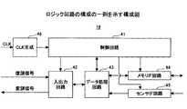
図2は、ロジック回路18の構成の一例を示す構成図である。図2に示すロジック回路18は、制御回路41、入出力回路42、データ処理回路43、メモリIF回路44、センサIF回路45、及びCLK生成回路46を含む。制御回路41は、入出力回路42、データ処理回路43、メモリIF回路44、及びセンサIF回路45の動作を制御する。 FIG. 2 is a configuration diagram illustrating an example of the configuration of the
クロック抽出回路28(図1参照)から供給されるクロック信号は、CLK生成回路46に供給される。CLK生成回路46は、例えば供給されたクロック信号を分周することにより、センサ付RFID用チップ200の各回路部分が同期して動作するためのクロック信号を生成する。 The clock signal supplied from the clock extraction circuit 28 (see FIG. 1) is supplied to the
データ復調回路24(図1参照)からの復調信号は入出力回路42により検知され、検知後のデータがデータ処理回路43に供給される。データ処理回路43は、供給されたデータを処理することで、このデータが指示するコマンド等を認識する。データ処理回路43は、受信コマンドを特定する信号を制御回路41に供給する。これに応じて制御回路41が、受信コマンドに従った制御動作を実行する。 The demodulated signal from the data demodulation circuit 24 (see FIG. 1) is detected by the input /
メモリIF回路44は、不揮発性メモリ14(図1参照)に対するデータの読み書きを実行するためのインターフェース回路である。またセンサIF回路45は、センサ回路16(図1参照)に対するデータ測定を指示したり、センサ回路16からの測定データを受け取ったりするためのインターフェース回路である。 The memory IF
データ処理回路43は、入出力回路42を介してリーダ・ライタ300側から供給されたデータ、センサ回路16からセンサIF回路45を介して受け取ったデータ、或いは不揮発性メモリ14からメモリIF回路44を介して受け取ったデータを内部レジスタに一次的に保持することができる。制御回路41は、コマンドに従った制御動作を実行することにより、データ処理回路43のレジスタのデータを、メモリIF回路44を介して不揮発性メモリ14に書き込んだり、入出力回路42及びデータ変調回路26を介してリーダ・ライタ300側に送信したりする。 The
図3は、リーダ・ライタ300の構成の一例を示す構成図である。図3のリーダ・ライタ300は、アンテナコイル51、出力モジュール52、変調器53、発信器54、フィルタ55、増幅器56、復調器57、制御器58、クロック抽出器59、入出力IF回路60を含む。 FIG. 3 is a configuration diagram showing an example of the configuration of the reader /
制御器58が、入出力IF回路60を介して外部(操作者或いはホスト装置)から送信データを受け取ると、変調器53に送信データを供給する。変調器53は、送信データを変調して変調データ信号を生成し、出力モジュール52に供給する。出力モジュール52は、変調データ信号をアンテナコイル51を介して送信する。この送信された信号は、センサ付RFID用チップ200によりアンテナコイル100で受信される。 When the
逆にセンサ付RFID用チップ200から送信された信号は、リーダ・ライタ300によりアンテナコイル51で受信される。受信信号は、フィルタ55によりフィルタ処理され、増幅器56により増幅され、更に復調器57により復調される。復調後の信号は、制御器58により入出力IF回路60を介して外部(操作者或いはホスト装置)に受信データとして供給される。 Conversely, a signal transmitted from the RFID chip with
このようにしてリーダ・ライタ300とセンサ付RFID用チップ200との間で無線通信により両方向にデータ転送することができる。センサ付RFID用チップ200からのデータはホスト装置(例えばコンピュータ)側に転送され、またセンサ付RFID用チップ200へのコマンド等のデータもホスト装置(例えばコンピュータ)側から転送されたものでよい。また或いは携帯型のリーダ・ライタ300であれば、センサ付RFID用チップ200からのデータは例えばリーダ・ライタ300が備える画面への表示により操作者に対して提示され、またセンサ付RFID用チップ200へのコマンド等のデータもリーダ・ライタ300が備えるキーパッドから操作者が入力したものであってよい。 In this way, data can be transferred in both directions between the reader /
本発明においては、図1乃至図3に例示したようなセンサ付RFID用チップ200及びリーダ・ライタ300を用い、センサ付RFID用チップ200のセンサ回路16によりデータを測定し、測定したデータを不揮発性メモリ14に記録する。またセンサ回路16からの測定データ又は不揮発性メモリ14に格納されている測定データをセンサ付RFID用チップ200からリーダ・ライタ300で読み出す。 In the present invention, the sensor-equipped
この際、センサ回路16のセンシング動作と、一般に最大の電力消費源である不揮発性メモリ14のアクセス動作とは、同時に実行されることがないように制御される。具体的には、センサ回路16によるデータ測定動作と不揮発性メモリ14への書き込み動作とが、同時に行われないように、各動作のタイミングが制御される。このタイミング制御は、ロジック回路18により実現されてよいし、またリーダ・ライタ300から供給するコマンド操作により実現されてよい。なお不揮発性メモリ14からの読み出し動作についても、センサ回路16によるデータ測定動作と同時に行われないように制御してよいことは当然である。 At this time, the sensing operation of the
センサ付RFID用チップ200のセンサは、例えば温度センサであってよい。この場合、センサ付RFID用チップ200は、生鮮食料品(野菜、肉、牛乳等)の出荷前に生鮮食料品に取り付けられてよい。これにより出荷後の流通過程において、生鮮食料品の温度が随時測定され、センサ付RFID用チップ200内のメモリに測定結果が順次記憶される。温度測定は、生鮮食料品の輸送中のトラックの荷台、生鮮食料品を保管する倉庫内、商店のショーケース内等で行なえばよい。具体的には、これらの温度測定位置において、リーダ・ライタ300から温度測定要求を無線で送信し、センサ付RFID用チップ200がこの要求に応答して温度を測定する。 The sensor of the RFID chip with
センサ回路16により測定された温度情報は、ロジック回路18を介して、不揮発性メモリ14に書き込まれる。不揮発性メモリ14は、半導体製造工場で書き込まれる固有ID(UID)領域の他に、無線タグが付けられている物品の固有情報(例えば食料品の場合、産地、生産者名、出荷日等)を書き込む固有領域と、流通・物流過程で測定される食料品の温度を記録する温度管理領域を有している。物品の固有情報は、リーダ・ライタ300から書き込み指示とともに供給され、不揮発性メモリ14に書き込まれる。また不揮発性メモリ14に格納されているデータは、リーダ・ライタ300により適宜読み出すことができる。 The temperature information measured by the
勿論、センサ回路16は温度センサである必要は無く、3軸センサ、圧力センサ、加速度センサ等の他のセンサであってよい。具体的には、RFID用チップの置かれた環境を示す何らかの物理的パラメータを検知可能な任意のセンサを、本発明に適用することができる。 Of course, the
図4は、本発明によるRFIDを用いたデータ測定動作の第1の実施例を示すフローチャートである。図4を用いて、RFIDを用いたデータ測定動作の第1の実施例について説明する。この第1の実施例は、センサ付RFID用チップ200のロジック回路18により、センサデータ測定動作と不揮発性メモリ書き込み動作とが同時に行われないように制御が実行される例である。 FIG. 4 is a flowchart showing a first embodiment of the data measurement operation using the RFID according to the present invention. A first embodiment of the data measurement operation using RFID will be described with reference to FIG. In the first embodiment, the
まずリーダ・ライタ300からタグ(センサ付RFID用チップ200及びアンテナコイル100)にセンサリードコマンドが供給される。センサリードコマンドはデータ復調回路24により復調され(S1)、復調後のデータがロジック回路18のデータ処理回路43により論理処理される(S2)。データ処理回路43によるセンサリードコマンドの論理処理結果(デコード処理結果)は制御回路41に供給され、これに応じて、制御回路41が各部を制御してセンサリード処理を実行する。 First, a sensor read command is supplied from the reader /
まずセンサ回路16が駆動され、センサ回路16によるデータ測定動作が実行される(S3)。センサ回路16が測定したデータはロジック回路18のセンサIF回路45を介してデータ処理回路43に供給される。測定データは、所定のデータ処理により所定の形式の測定データに変換されるとともに、データ処理回路43に一時的に保持される(S4)。 First, the
センサ回路16による測定動作が終了すると、センサ回路16の動作停止後に、不揮発性メモリ14に対する測定データの書き込み処理を実行する(S5)。具体的には、データ処理回路43に一時的に保持されている測定データを、メモリIF回路44を介して不揮発性メモリ14に転送するとともに、ロジック回路18からメモリ書き込み指示を不揮発性メモリ14に与えることで、不揮発性メモリ14に対する測定データ書き込みが実行される。 When the measurement operation by the
その後、データ処理回路43に一時的に保持されている測定データは更に、入出力回路42を介してデータ変調回路26に供給され、データ変調回路26により変調処理が施される(S6)。変調された測定データは、アンテナコイル100を介してリーダ・ライタ300に送信される。 Thereafter, the measurement data temporarily held in the
上記データ測定動作において、ロジック回路18は、データ測定コマンドを受信・検出するために必要な回路であり、平滑キャパシタC2から供給される電力で動作する。この際、平滑キャパシタC3から供給される電力で動作するセンサ回路16や不揮発性メモリ14の動作電圧より低い電圧で動作できるように設計されている。電源制御回路30は、擬似負荷として機能するデジタルボリュームや、負荷の変動に応じた電圧制御をするシリ−ズレギュレータ等を備え、これらのデジタルボリュームやシリ−ズレギュレータ等の働きにより、一定の直流電圧を負荷に供給するように機能する。 In the data measurement operation, the
ロジック回路18は、センサ回路16の動作開始より前に動作を開始して、電源制御回路30により所定の電圧になるよう制御された平滑キャパシタC2の電力で駆動される。電源制御回路30は、センサ回路16の動作用として、ロジック回路18の動作電圧より高い所定の電圧を平滑キャパシタC3に確保する。ロジック回路18からセンサ動作(データ測定動作)開始要求が出されると、センサ回路16は、電源制御回路30により所定の電圧になるよう制御された平滑キャパシタC3の電力で動作して、データを測定する。次にロジック回路18からデータ書き込み要求が出されると、不揮発性メモリ14が、電源制御回路30により所定の電圧になるよう制御された平滑キャパシタC3の電力で動作して、ロジック回路18から供給されたデータを格納する。 The
一般的に、センサ回路16が設けられていないセンサ付RFID用チップにおいては、不揮発性メモリ14への書き込みに必要な消費電力が一番大きい。従って、不揮発性メモリ14への書き込みの消費電力の大きさが、センサ付RFID用チップの通信距離を決定する要素となる。これを鑑みると、センサ回路16の動作に必要な消費電力については、不揮発性メモリ14の消費電力と同等若しくはそれ以下に設定し、センサ回路16と不揮発性メモリ14の動作が時間的に重ならないように動作制御すれば、通信距離性能を劣化させること無く、センサ回路16を内蔵したセンサ付RFID用チップを提供することができる。 In general, in the RFID chip with sensor in which the
上記第1の実施例においては、センサ付RFID用チップ200のロジック回路18がセンサ回路16のセンシング動作及び不揮発性メモリ14の書き込み動作を制御して、これらの動作が互いに時間的に重ならないようにしている。従って、センサ回路16が設けられていない場合と比較して、通信距離を落とすことなく、センサ機能をセンサ付RFID用チップに内蔵することができる。 In the first embodiment, the
図5は、本発明によるRFIDを用いたデータ測定動作の第2の実施例を示すフローチャートである。図5を用いて、RFIDを用いたデータ測定動作の第2の実施例について説明する。この第2の実施例は、リーダ・ライタ300により、センサデータ測定動作と不揮発性メモリ書き込み動作とが同時に行われないように制御が実行される例である。 FIG. 5 is a flowchart showing a second embodiment of the data measurement operation using the RFID according to the present invention. A second embodiment of the data measurement operation using RFID will be described with reference to FIG. In the second embodiment, the reader /
まずリーダ・ライタ300からタグ(センサ付RFID用チップ200及びアンテナコイル100)にセンサリードコマンドが供給される。センサリードコマンドはデータ復調回路24により復調され(S1)、復調後のデータがロジック回路18のデータ処理回路43により論理処理される(S2)。データ処理回路43によるセンサリードコマンドの論理処理結果(デコード処理結果)は制御回路41に供給され、これに応じて、制御回路41が各部を制御してセンサリード処理を実行する。 First, a sensor read command is supplied from the reader /
まずセンサ回路16が駆動され、センサ回路16によるデータ測定動作が実行される(S3)。センサ回路16が測定したデータはロジック回路18のセンサIF回路45を介してデータ処理回路43に供給される。測定データは、所定のデータ処理により所定の形式の測定データに変換されるとともに、データ処理回路43に一時的に保持される(S4)。 First, the
データ処理回路43に一時的に保持されている測定データは更に、入出力回路42を介してデータ変調回路26に供給され、データ変調回路26により変調処理が施される(S5)。変調された測定データは、アンテナコイル100を介してリーダ・ライタ300に送信される。 The measurement data temporarily held in the
リーダ・ライタ300は、測定データをセンサ付RFID用チップ200から受け取った後、センサ付RFID用チップ200に対してライトコマンドを送信する。ライトコマンドはデータ復調回路24により復調され(S6)、復調後のデータがロジック回路18のデータ処理回路43により論理処理される(S7)。データ処理回路43によるライトコマンドの論理処理結果(デコード処理結果)は制御回路41に供給され、これに応じて、制御回路41が各部を制御してライト処理を実行する。 After receiving the measurement data from the RFID chip with
ライト処理においては、まず、不揮発性メモリ14に対する測定データの書き込み処理を実行する(S8)。具体的には、上記センサリード処理によりデータ処理回路43に一時的に保持されている測定データを、メモリIF回路44を介して不揮発性メモリ14に転送するとともに、ロジック回路18からメモリ書き込み指示を不揮発性メモリ14に与えることで、不揮発性メモリ14に対する測定データ書き込みが実行される。或いは、上記センサリード処理によりリーダ・ライタ300が取得した測定データを、上記ライトコマンドとともにセンサ付RFID用チップ200に転送し、この転送されたデータを不揮発性メモリ14に書き込むようにしてもよい。 In the write process, first, a process of writing measurement data to the
その後、データ処理回路43に一時的に保持されている測定データは、必要に応じて所定のデータ処理に供され(S9)、入出力回路42を介してデータ変調回路26に供給され、データ変調回路26により変調処理が施される(S10)。変調された測定データは、アンテナコイル100を介してリーダ・ライタ300に送信される。 After that, the measurement data temporarily stored in the
上記データ測定・メモリ書き込み動作において、センサ回路16の動作に必要な消費電力については、不揮発性メモリ14の消費電力と同等若しくはそれ以下に設定することが望ましい。この第2の実施例においては、リーダ・ライタ300がセンサ回路16のセンシング動作及び不揮発性メモリ14の書き込み動作を制御して、これらの動作が互いに時間的に重ならないようにしている。従って、センサ回路16が設けられていない場合と比較して通信距離を落とすことなく、センサ機能をセンサ付RFID用チップに内蔵することができる。 In the data measurement / memory writing operation, the power consumption necessary for the operation of the
以上、本発明を実施例に基づいて説明したが、本発明は上記実施例に限定されるものではなく、特許請求の範囲に記載の範囲内で様々な変形が可能である。 As mentioned above, although this invention was demonstrated based on the Example, this invention is not limited to the said Example, A various deformation | transformation is possible within the range as described in a claim.
なお本発明は、以下の内容を含むものである。
(付記1)
アンテナに結合され該アンテナからの交流電圧を直流電圧に変換するよう機能する整流回路と、
該整流回路に結合され該直流電圧で動作する不揮発性メモリと、
該整流回路に結合され該直流電圧で動作し所定のデータを測定するセンサ回路と、
該不揮発性メモリのアクセス動作と該センサ回路のデータ測定動作とが同時に実行されないように該不揮発性メモリと該センサ回路とを制御するロジック回路
を含むことを特徴とする集積回路チップ。
(付記2)
該不揮発性メモリの該アクセス動作は該不揮発性メモリに対するデータ書き込み動作であることを特徴とする付記1記載の集積回路チップ。
(付記3)
該ロジック回路は、該アンテナから受信した所定のコマンドに応答して、該センサ回路に該データ測定動作を実行させ、該データ測定動作が終了した後に、該不揮発性メモリに該データ測定動作により得られた測定データを書き込む該アクセス動作を実行することを特徴とする付記2記載の集積回路チップ。
(付記4)
該ロジック回路は、該データ測定動作により得られた該測定データを一時的に保持するレジスタを含むことを特徴とする付記3記載の集積回路チップ。
(付記5)
該センサ回路が該データ測定動作を実行することにより消費する電力は該不揮発性メモリが該アクセス動作を実行することにより消費する電力よりも小さいことを特徴とする付記1記載の集積回路チップ。
(付記6)
電波を送受信するリーダ・ライタと、
該リーダ・ライタと該電波を介して通信するICタグ
を含み、該ICタグは、
アンテナと、
該アンテナに結合され該アンテナが受信した該電波の交流電圧を直流電圧に変換するよう機能する整流回路と、
該整流回路に結合され該直流電圧で動作する不揮発性メモリと、
該整流回路に結合され該直流電圧で動作し所定のデータを測定するセンサ回路
を含み、該不揮発性メモリのアクセス動作と該センサ回路のデータ測定動作とが同時に実行されないように制御されることを特徴とするRFIDシステム。
(付記7)
該リーダ・ライタは、第1の所定のコマンドを該ICタグに送信して該センサ回路に該データ測定動作を実行させ、該データ測定動作が終了した後に、第2の所定のコマンドを該ICタグに送信して該不揮発性メモリに該データ測定動作により得られた測定データを書き込む該アクセス動作を実行させることを特徴とする付記6記載のRFIDシステム。(付記8)
リーダ・ライタとの間で電波を送受信するICタグにおいて、
アンテナと、
該アンテナに結合され該アンテナが受信した該電波の交流電圧を直流電圧に変換するよう機能する整流回路と、
該整流回路に結合され該直流電圧で動作する不揮発性メモリと、
該整流回路に結合され該直流電圧で動作し所定のデータを測定するセンサ回路
を含み、該不揮発性メモリのアクセス動作と該センサ回路のデータ測定動作とが同時に実行されないように制御されることを特徴とするICタグ。
(付記9)
該不揮発性メモリの該アクセス動作は該不揮発性メモリに対するデータ書き込み動作であることを特徴とする付記8記載のICタグ。
(付記10)
該ロジック回路は、該データ測定動作により得られた該測定データを一時的に保持するレジスタを含むことを特徴とする付記9記載のICタグ。
(付記11)
該センサ回路が該データ測定動作を実行することにより消費する電力は該不揮発性メモリが該アクセス動作を実行することにより消費する電力よりも小さいことを特徴とする付記6記載のRFIDシステム。The present invention includes the following contents.
(Appendix 1)
A rectifier circuit coupled to the antenna and functioning to convert an alternating voltage from the antenna into a direct current voltage;
A non-volatile memory coupled to the rectifier circuit and operating at the DC voltage;
A sensor circuit coupled to the rectifier circuit and operating on the DC voltage to measure predetermined data;
An integrated circuit chip, comprising: a logic circuit that controls the nonvolatile memory and the sensor circuit so that an access operation of the nonvolatile memory and a data measurement operation of the sensor circuit are not performed simultaneously.
(Appendix 2)
The integrated circuit chip according to appendix 1, wherein the access operation of the nonvolatile memory is a data write operation to the nonvolatile memory.
(Appendix 3)
In response to a predetermined command received from the antenna, the logic circuit causes the sensor circuit to perform the data measurement operation, and after the data measurement operation is completed, the logic circuit obtains the data measurement operation in the nonvolatile memory. The integrated circuit chip according to
(Appendix 4)
4. The integrated circuit chip according to appendix 3, wherein the logic circuit includes a register that temporarily holds the measurement data obtained by the data measurement operation.
(Appendix 5)
The integrated circuit chip according to claim 1, wherein power consumed by the sensor circuit executing the data measurement operation is smaller than power consumed by the nonvolatile memory executing the access operation.
(Appendix 6)
A reader / writer that transmits and receives radio waves,
An IC tag that communicates with the reader / writer via the radio wave,
An antenna,
A rectifier circuit coupled to the antenna and functioning to convert the alternating voltage of the radio wave received by the antenna into a direct current voltage;
A non-volatile memory coupled to the rectifier circuit and operating at the DC voltage;
A sensor circuit which is coupled to the rectifier circuit and operates with the DC voltage and measures predetermined data, and is controlled so that an access operation of the nonvolatile memory and a data measurement operation of the sensor circuit are not performed simultaneously; A featured RFID system.
(Appendix 7)
The reader / writer transmits a first predetermined command to the IC tag to cause the sensor circuit to execute the data measurement operation. After the data measurement operation is completed, the reader / writer sends a second predetermined command to the IC tag. The RFID system according to
In an IC tag that transmits and receives radio waves to and from a reader / writer,
An antenna,
A rectifier circuit coupled to the antenna and functioning to convert the alternating voltage of the radio wave received by the antenna into a direct current voltage;
A non-volatile memory coupled to the rectifier circuit and operating at the DC voltage;
A sensor circuit which is coupled to the rectifier circuit and operates with the DC voltage and measures predetermined data, and is controlled so that an access operation of the nonvolatile memory and a data measurement operation of the sensor circuit are not performed simultaneously; Characteristic IC tag.
(Appendix 9)
9. The IC tag according to appendix 8, wherein the access operation of the nonvolatile memory is a data write operation to the nonvolatile memory.
(Appendix 10)
The IC tag according to appendix 9, wherein the logic circuit includes a register that temporarily holds the measurement data obtained by the data measurement operation.
(Appendix 11)
The RFID system according to
10 アンテナ端子
12 整流回路
14 不揮発性メモリ
16 センサ回路
18 ロジック回路
22 データ制御回路
30 電源制御回路
100 アンテナコイル
200 センサ付RFID用チップ
300 リーダ・ライタ30010
Claims (10)
Translated fromJapanese該整流回路に結合され該直流電圧で動作する不揮発性メモリと、
該整流回路に結合され該直流電圧で動作し所定のデータを測定するセンサ回路と、
該不揮発性メモリのアクセス動作と該センサ回路のデータ測定動作とが同時に実行されないように該不揮発性メモリと該センサ回路とを制御するロジック回路
を含むことを特徴とする集積回路チップ。A rectifier circuit coupled to the antenna and functioning to convert an alternating voltage from the antenna into a direct current voltage;
A non-volatile memory coupled to the rectifier circuit and operating at the DC voltage;
A sensor circuit coupled to the rectifier circuit and operating on the DC voltage to measure predetermined data;
An integrated circuit chip, comprising: a logic circuit that controls the nonvolatile memory and the sensor circuit so that an access operation of the nonvolatile memory and a data measurement operation of the sensor circuit are not performed simultaneously.
該リーダ・ライタと該電波を介して通信するICタグ
を含み、該ICタグは、
アンテナと、
該アンテナに結合され該アンテナが受信した該電波の交流電圧を直流電圧に変換するよう機能する整流回路と、
該整流回路に結合され該直流電圧で動作する不揮発性メモリと、
該整流回路に結合され該直流電圧で動作し所定のデータを測定するセンサ回路
を含み、該不揮発性メモリのアクセス動作と該センサ回路のデータ測定動作とが同時に実行されないように制御されることを特徴とするRFIDシステム。A reader / writer that transmits and receives radio waves,
An IC tag that communicates with the reader / writer via the radio wave,
An antenna,
A rectifier circuit coupled to the antenna and functioning to convert the alternating voltage of the radio wave received by the antenna into a direct current voltage;
A non-volatile memory coupled to the rectifier circuit and operating at the DC voltage;
A sensor circuit which is coupled to the rectifier circuit and operates with the DC voltage and measures predetermined data, and is controlled so that an access operation of the nonvolatile memory and a data measurement operation of the sensor circuit are not performed simultaneously; A featured RFID system.
アンテナと、
該アンテナに結合され該アンテナが受信した該電波の交流電圧を直流電圧に変換するよう機能する整流回路と、
該整流回路に結合され該直流電圧で動作する不揮発性メモリと、
該整流回路に結合され該直流電圧で動作し所定のデータを測定するセンサ回路
を含み、該不揮発性メモリのアクセス動作と該センサ回路のデータ測定動作とが同時に実行されないように制御されることを特徴とするICタグ。In an IC tag that transmits and receives radio waves to and from a reader / writer,
An antenna,
A rectifier circuit coupled to the antenna and functioning to convert the alternating voltage of the radio wave received by the antenna into a direct current voltage;
A non-volatile memory coupled to the rectifier circuit and operating at the DC voltage;
A sensor circuit which is coupled to the rectifier circuit and operates with the DC voltage and measures predetermined data, and is controlled so that an access operation of the nonvolatile memory and a data measurement operation of the sensor circuit are not performed simultaneously; Characteristic IC tag.
The IC tag according to claim 9, further comprising a register that temporarily holds measurement data obtained by the data measurement operation.
Priority Applications (2)
| Application Number | Priority Date | Filing Date | Title |
|---|---|---|---|
| JP2005316806AJP2007122600A (en) | 2005-10-31 | 2005-10-31 | Integrated circuit chip and RFID system |
| US11/360,601US7688182B2 (en) | 2005-10-31 | 2006-02-24 | RFID system and RFID chip equipped with sensor function |
Applications Claiming Priority (1)
| Application Number | Priority Date | Filing Date | Title |
|---|---|---|---|
| JP2005316806AJP2007122600A (en) | 2005-10-31 | 2005-10-31 | Integrated circuit chip and RFID system |
Publications (1)
| Publication Number | Publication Date |
|---|---|
| JP2007122600Atrue JP2007122600A (en) | 2007-05-17 |
Family
ID=37995534
Family Applications (1)
| Application Number | Title | Priority Date | Filing Date |
|---|---|---|---|
| JP2005316806APendingJP2007122600A (en) | 2005-10-31 | 2005-10-31 | Integrated circuit chip and RFID system |
Country Status (2)
| Country | Link |
|---|---|
| US (1) | US7688182B2 (en) |
| JP (1) | JP2007122600A (en) |
Cited By (2)
| Publication number | Priority date | Publication date | Assignee | Title |
|---|---|---|---|---|
| JP2011118536A (en)* | 2009-12-01 | 2011-06-16 | Mega Chips Corp | Sensor device and semiconductor device |
| US10909434B2 (en) | 2019-03-29 | 2021-02-02 | Lapis Semiconductor Co., Ltd. | Passive RFID tag and RFID system |
Families Citing this family (37)
| Publication number | Priority date | Publication date | Assignee | Title |
|---|---|---|---|---|
| GB0501115D0 (en)* | 2005-01-19 | 2005-02-23 | Innovision Res & Tech Plc | Combined power coupling and rf communication apparatus |
| AT8411U3 (en)* | 2006-03-02 | 2007-03-15 | Avl List Gmbh | TEST BENCH SENSOR DEVICE, AND TEST BENCH, PREFERABLY FOR POWER MACHINES |
| KR100764438B1 (en)* | 2006-07-18 | 2007-10-05 | 주식회사 하이닉스반도체 | RFID device |
| JP5008201B2 (en)* | 2008-05-21 | 2012-08-22 | 三智商事株式会社 | Wireless IC tag |
| US8514060B2 (en)* | 2008-05-21 | 2013-08-20 | Mitomo Corporation | Wireless identification tag |
| US8284028B2 (en)* | 2008-08-14 | 2012-10-09 | Icopal Danmark A/S | Method of manufacturing an identifiable roofing product including a roofing product and a process plant for carrying out the method |
| JP5385298B2 (en)* | 2008-10-29 | 2014-01-08 | 株式会社日立製作所 | Frequency variable Fresnel region power transmitter and receiver, and power transmission system |
| SI22957A (en)* | 2009-01-07 | 2010-07-30 | Ids D.O.O. | Procedure for secure durable process registration within an active rfid label inside a labelled object |
| FI124073B (en)* | 2010-09-17 | 2014-03-14 | Stora Enso Oyj | Intelligent packaging |
| EP2543974B1 (en)* | 2011-07-06 | 2014-02-26 | Nxp B.V. | Metering system having improved security |
| US9151741B2 (en) | 2011-11-02 | 2015-10-06 | Avery Dennison Corporation | RFID-based devices and methods for initializing a sensor |
| US9254583B2 (en) | 2012-01-23 | 2016-02-09 | Quipip, Llc | Systems, methods and apparatus for providing comparative statistical information for a plurality of production facilities in a closed-loop production management system |
| US9836801B2 (en) | 2012-01-23 | 2017-12-05 | Quipip, Llc | Systems, methods and apparatus for providing comparative statistical information in a graphical format for a plurality of markets using a closed-loop production management system |
| FI127537B (en)* | 2012-04-11 | 2018-08-31 | Marisense Oy | Electronic label tag and electronic label tag system |
| DE102012014584A1 (en)* | 2012-07-23 | 2014-01-23 | Hottinger Baldwin Messtechnik Gmbh | Measured variable sensor with internal data memory |
| US9024730B2 (en)* | 2012-09-04 | 2015-05-05 | Honeywell International Inc. | Standby activation |
| KR101759806B1 (en) | 2012-11-01 | 2017-07-19 | 블루 스파크 테크놀러지스, 인크. | Body temperature logging patch |
| CN104516381B (en)* | 2013-09-26 | 2016-04-27 | 上海华虹集成电路有限责任公司 | Regulator rectifier circuit in radio-frequency (RF) identification |
| US9429559B2 (en)* | 2014-01-29 | 2016-08-30 | Quipip, Llc | Systems, methods and apparatus for obtaining data relating to condition and performance of concrete mixtures |
| US10184928B2 (en) | 2014-01-29 | 2019-01-22 | Quipip, Llc | Measuring device, systems, and methods for obtaining data relating to condition and performance of concrete mixtures |
| US9194855B2 (en) | 2014-02-28 | 2015-11-24 | Quipip, Llc | Systems, methods and apparatus for providing to a driver of a vehicle carrying a mixture real-time information relating to a characteristic of the mixture |
| JP2017530441A (en)* | 2014-08-04 | 2017-10-12 | アベリー・デニソン・コーポレイションAvery Dennison Corporation | Time-temperature tracking label |
| US9937124B2 (en) | 2014-09-11 | 2018-04-10 | International Business Machines Corporation | Microchip substance delivery devices having low-power electromechanical release mechanisms |
| US9693689B2 (en) | 2014-12-31 | 2017-07-04 | Blue Spark Technologies, Inc. | Body temperature logging patch |
| WO2016123228A1 (en) | 2015-01-30 | 2016-08-04 | Quipip, Llc | Systems, apparatus and methods for testing and predicting the performance of concrete mixtures |
| US9734371B2 (en) | 2015-03-31 | 2017-08-15 | International Business Machines Corporation | Hybrid tag for radio frequency identification system |
| US9755701B2 (en)* | 2015-03-31 | 2017-09-05 | International Business Machines Corporation | Hybrid tag for radio frequency identification system |
| FR3038185B1 (en)* | 2015-06-25 | 2018-08-17 | Connecthings | SENSOR EMITTING TO A MOBILE PHONE |
| US10881788B2 (en) | 2015-10-30 | 2021-01-05 | International Business Machines Corporation | Delivery device including reactive material for programmable discrete delivery of a substance |
| US9928696B2 (en) | 2015-12-30 | 2018-03-27 | Immersion Corporation | Externally-activated haptic devices and systems |
| US20170350241A1 (en)* | 2016-05-13 | 2017-12-07 | Ningbo Wanyou Deepwater Energy Science & Technology Co.,Ltd. | Data Logger and Charger Thereof |
| US20170328197A1 (en)* | 2016-05-13 | 2017-11-16 | Ningbo Wanyou Deepwater Energy Science & Technolog Co.,Ltd. | Data Logger, Manufacturing Method Thereof and Real-time Measurement System Thereof |
| CN112836780A (en)* | 2016-12-07 | 2021-05-25 | 四川谦泰仁投资管理有限公司 | RFID chip with interactive switch input port and sensor induction unit |
| US10849501B2 (en) | 2017-08-09 | 2020-12-01 | Blue Spark Technologies, Inc. | Body temperature logging patch |
| US10664669B2 (en)* | 2018-01-30 | 2020-05-26 | Idex Biometrics Asa | Device architecture |
| FR3108408B1 (en)* | 2020-03-18 | 2022-03-25 | Asygn | Passive RFID tag circuit comprising a strain sensor and method for making a circuit |
| US12167904B2 (en)* | 2020-04-22 | 2024-12-17 | Biotags, LLC | Temperature sensor patch and system |
Citations (5)
| Publication number | Priority date | Publication date | Assignee | Title |
|---|---|---|---|---|
| JPH0855198A (en)* | 1994-08-15 | 1996-02-27 | Hitachi Ltd | Non-contact IC card |
| JP2000306188A (en)* | 1999-04-26 | 2000-11-02 | Yokohama Rubber Co Ltd:The | Transponder element and transponder |
| JP2003132316A (en)* | 2001-10-29 | 2003-05-09 | Fujitsu Ltd | Information processing apparatus and card type information processing device |
| JP2003302290A (en)* | 2002-04-11 | 2003-10-24 | Dainippon Printing Co Ltd | Temperature measurement data carrier, method for manufacturing the same, temperature measurement method, and temperature measurement system |
| JP2004024551A (en)* | 2002-06-26 | 2004-01-29 | Renesas Technology Corp | Semiconductor device for sensor system |
Family Cites Families (9)
| Publication number | Priority date | Publication date | Assignee | Title |
|---|---|---|---|---|
| US5731754A (en)* | 1994-06-03 | 1998-03-24 | Computer Methods Corporation | Transponder and sensor apparatus for sensing and transmitting vehicle tire parameter data |
| US5483827A (en)* | 1994-06-03 | 1996-01-16 | Computer Methods Corporation | Active integrated circuit transponder and sensor apparatus for sensing and transmitting vehicle tire parameter data |
| US6249212B1 (en)* | 1994-10-05 | 2001-06-19 | Avid Marketing, Inc. | Universal electronic identification tag |
| US5606323A (en)* | 1995-08-31 | 1997-02-25 | International Business Machines Corporation | Diode modulator for radio frequency transponder |
| US6617963B1 (en)* | 1999-02-26 | 2003-09-09 | Sri International | Event-recording devices with identification codes |
| US6720866B1 (en)* | 1999-03-30 | 2004-04-13 | Microchip Technology Incorporated | Radio frequency identification tag device with sensor input |
| JP4273636B2 (en)* | 2000-06-30 | 2009-06-03 | ソニー株式会社 | Information recording apparatus and method, and information recording system |
| JP2004164050A (en) | 2002-11-11 | 2004-06-10 | Nippon Telegr & Teleph Corp <Ntt> | Data carrier with temperature and humidity sensor and temperature and humidity sensing system |
| US7716160B2 (en)* | 2003-11-07 | 2010-05-11 | Alien Technology Corporation | Methods and apparatuses to identify devices |
- 2005
- 2005-10-31JPJP2005316806Apatent/JP2007122600A/enactivePending
- 2006
- 2006-02-24USUS11/360,601patent/US7688182B2/ennot_activeExpired - Fee Related
Patent Citations (5)
| Publication number | Priority date | Publication date | Assignee | Title |
|---|---|---|---|---|
| JPH0855198A (en)* | 1994-08-15 | 1996-02-27 | Hitachi Ltd | Non-contact IC card |
| JP2000306188A (en)* | 1999-04-26 | 2000-11-02 | Yokohama Rubber Co Ltd:The | Transponder element and transponder |
| JP2003132316A (en)* | 2001-10-29 | 2003-05-09 | Fujitsu Ltd | Information processing apparatus and card type information processing device |
| JP2003302290A (en)* | 2002-04-11 | 2003-10-24 | Dainippon Printing Co Ltd | Temperature measurement data carrier, method for manufacturing the same, temperature measurement method, and temperature measurement system |
| JP2004024551A (en)* | 2002-06-26 | 2004-01-29 | Renesas Technology Corp | Semiconductor device for sensor system |
Cited By (3)
| Publication number | Priority date | Publication date | Assignee | Title |
|---|---|---|---|---|
| JP2011118536A (en)* | 2009-12-01 | 2011-06-16 | Mega Chips Corp | Sensor device and semiconductor device |
| US10909434B2 (en) | 2019-03-29 | 2021-02-02 | Lapis Semiconductor Co., Ltd. | Passive RFID tag and RFID system |
| US11599759B2 (en) | 2019-03-29 | 2023-03-07 | Lapis Semiconductor Co., Ltd. | Passive RFID tag and RFID system |
Also Published As
| Publication number | Publication date |
|---|---|
| US20070096880A1 (en) | 2007-05-03 |
| US7688182B2 (en) | 2010-03-30 |
Similar Documents
| Publication | Publication Date | Title |
|---|---|---|
| JP2007122600A (en) | Integrated circuit chip and RFID system | |
| KR100833511B1 (en) | Passive tag with volatile memory | |
| KR101138836B1 (en) | Rfid tag | |
| US20070194936A1 (en) | Contactless communication scheme and contactless communication system | |
| TWI596546B (en) | Rfid card learning apparatus, wearable produc and operating method thereof | |
| US8269608B2 (en) | Device and method of coupling a processor to an RFID tag | |
| JP2007172654A (en) | RF-ID system and method capable of confirming additional information | |
| CN111325302B (en) | Passive wireless magnetic field characteristic sensing tag and sensing system | |
| JP2008024385A (en) | Goods management system | |
| JP6229265B2 (en) | RFID tag system and temperature detection method | |
| KR101204091B1 (en) | RFID system preventing recognition error and communication method thereof | |
| CN104700136B (en) | Article stowed location automatic station-keeping system and method | |
| JP4983017B2 (en) | Information access system and method for accessing information in a contactless information storage device | |
| JP2006060283A (en) | Communication auxiliary assembly, communication auxiliary system, and communication method | |
| CN103852185A (en) | Intelligent sensor which has RFID function and can store temperature value | |
| US20100013605A1 (en) | Data carrier and data carrier system | |
| JP2006039789A (en) | Non-contact data carrier with temperature change detection function | |
| RU2713864C1 (en) | Combined sensor rfid-label | |
| JP6147713B2 (en) | RFID tag, pre-shipment management system, and pre-shipment management method | |
| JP6314459B2 (en) | Information recording apparatus and recorded information management method | |
| JP2011107894A (en) | Rfid system and anti-collision processing method | |
| JP6506158B2 (en) | Parts management system | |
| JP6254472B2 (en) | RFID tag | |
| Nan et al. | A method of applying an RFID electronic tag with an IIC interface | |
| KR20130039158A (en) | Radio frequency identification tag |
Legal Events
| Date | Code | Title | Description |
|---|---|---|---|
| A711 | Notification of change in applicant | Free format text:JAPANESE INTERMEDIATE CODE: A712 Effective date:20080729 | |
| A977 | Report on retrieval | Free format text:JAPANESE INTERMEDIATE CODE: A971007 Effective date:20090326 | |
| A131 | Notification of reasons for refusal | Free format text:JAPANESE INTERMEDIATE CODE: A131 Effective date:20090407 | |
| A521 | Written amendment | Free format text:JAPANESE INTERMEDIATE CODE: A523 Effective date:20090604 | |
| A02 | Decision of refusal | Free format text:JAPANESE INTERMEDIATE CODE: A02 Effective date:20091208 | |
| A521 | Written amendment | Free format text:JAPANESE INTERMEDIATE CODE: A523 Effective date:20100305 | |
| A911 | Transfer to examiner for re-examination before appeal (zenchi) | Free format text:JAPANESE INTERMEDIATE CODE: A911 Effective date:20100315 | |
| A912 | Re-examination (zenchi) completed and case transferred to appeal board | Free format text:JAPANESE INTERMEDIATE CODE: A912 Effective date:20100528 |