JP2007121490A - Liquid crystal display element - Google Patents
Liquid crystal display elementDownload PDFInfo
- Publication number
- JP2007121490A JP2007121490AJP2005310976AJP2005310976AJP2007121490AJP 2007121490 AJP2007121490 AJP 2007121490AJP 2005310976 AJP2005310976 AJP 2005310976AJP 2005310976 AJP2005310976 AJP 2005310976AJP 2007121490 AJP2007121490 AJP 2007121490A
- Authority
- JP
- Japan
- Prior art keywords
- liquid crystal
- display element
- crystal display
- retardation
- axis
- Prior art date
- Legal status (The legal status is an assumption and is not a legal conclusion. Google has not performed a legal analysis and makes no representation as to the accuracy of the status listed.)
- Pending
Links
- 239000004973liquid crystal related substanceSubstances0.000titleclaimsabstractdescription396
- 210000002858crystal cellAnatomy0.000claimsabstractdescription83
- 239000000758substrateSubstances0.000claimsabstractdescription46
- 238000010521absorption reactionMethods0.000claimsdescription20
- 239000011159matrix materialSubstances0.000claimsdescription8
- 238000002834transmittanceMethods0.000description67
- 238000011156evaluationMethods0.000description55
- 230000000052comparative effectEffects0.000description31
- 230000003287optical effectEffects0.000description13
- 238000004519manufacturing processMethods0.000description11
- 230000007423decreaseEffects0.000description8
- 230000035699permeabilityEffects0.000description8
- 239000000463materialSubstances0.000description7
- 229920005668polycarbonate resinPolymers0.000description6
- 239000004431polycarbonate resinSubstances0.000description6
- 229920000642polymerPolymers0.000description6
- 230000008859changeEffects0.000description4
- 230000005684electric fieldEffects0.000description2
- 239000011521glassSubstances0.000description2
- 238000000034methodMethods0.000description2
- 208000011823Juvenile amyotrophic lateral sclerosisDiseases0.000description1
- 229910004298SiO 2Inorganic materials0.000description1
- 229910010413TiO 2Inorganic materials0.000description1
- 230000005540biological transmissionEffects0.000description1
- 230000015572biosynthetic processEffects0.000description1
- AMGQUBHHOARCQH-UHFFFAOYSA-Nindium;oxotinChemical compound[In].[Sn]=OAMGQUBHHOARCQH-UHFFFAOYSA-N0.000description1
- 230000004048modificationEffects0.000description1
- 238000012986modificationMethods0.000description1
- 230000008569processEffects0.000description1
- 230000009467reductionEffects0.000description1
- 229920005989resinPolymers0.000description1
- 239000011347resinSubstances0.000description1
- 238000003980solgel methodMethods0.000description1
- 125000006850spacer groupChemical group0.000description1
Images


Landscapes
- Polarising Elements (AREA)
- Liquid Crystal (AREA)
Abstract
Description
Translated fromJapanese本発明は、液晶表示素子に関し、特に、車載用途にも使用可能なVAモード液晶表示素子に関する。 The present invention relates to a liquid crystal display element, and more particularly to a VA mode liquid crystal display element that can be used for in-vehicle applications.
一般に、透過型の液晶表示素子は、所定の方向に配向した数μm程度の極薄い液晶層と、この液晶層を挟持する透明な一対の薄い基板と、さらに、この基板を挟持して偏光子および検光子を構成する一対の偏光板とを有する。ここで、液晶層が設けられる側の基板面には、所定の形状にパターニングされた電極が形成されている。そして、この電極を介して液晶層に電圧を印加すると、液晶の配向が変化して、液晶表示素子を透過する光の量または波長が変わる。これにより、所望の表示を行うことが可能となる。 In general, a transmissive liquid crystal display element includes an extremely thin liquid crystal layer of about several μm oriented in a predetermined direction, a pair of transparent thin substrates that sandwich the liquid crystal layer, and a polarizer that sandwiches the substrate. And a pair of polarizing plates constituting the analyzer. Here, an electrode patterned in a predetermined shape is formed on the substrate surface on the side where the liquid crystal layer is provided. When a voltage is applied to the liquid crystal layer through this electrode, the alignment of the liquid crystal changes, and the amount or wavelength of light transmitted through the liquid crystal display element changes. Thereby, a desired display can be performed.
このように、液晶表示素子は、比較的単純な構造からなっている。また、構成部材の選択によって薄型化および軽量化が容易であり、また、低電圧での駆動も可能であることから、近年では、民生用のみならず車載用の表示素子としても盛んに利用されている。 Thus, the liquid crystal display element has a relatively simple structure. In addition, since it is easy to reduce the thickness and weight by selecting components, and it is possible to drive at a low voltage, in recent years, it has been actively used as a display element for in-vehicle use as well as consumer use. ing.
ところで、液晶表示素子は、液晶層の初期配向状態並びに電圧印加時の動作状態および配向状態などから、いくつかのモードに分類される。例えば、液晶テレビや、自動車などの車両のインストルメントパネルなどいわゆる車載用に利用される液晶表示素子には、VA(Vertical Alignment)モードが用いられる(例えば、特許文献1および2参照。)。VAモードは、正面から見たときのコントラスト比が高く、また、視野角が広いことから、視認性に優れたモードである。 By the way, liquid crystal display elements are classified into several modes based on the initial alignment state of the liquid crystal layer, the operation state and the alignment state when a voltage is applied, and the like. For example, a VA (Vertical Alignment) mode is used for so-called in-vehicle liquid crystal display elements such as liquid crystal televisions and instrument panels of vehicles such as automobiles (see, for example,
VAモードは、一対の基板間に、初期配向状態が基板と概ね垂直(垂直配向)な負の誘電率異方性(△ε)を有する液晶層を挟持し、さらに、この基板を、通常はクロスニコルを構成するように配置した一対の偏光板で挟持することによって構成される。そして、基板面に形成された電極を介して液晶層に電圧を印加すると、液晶の配向が変化して、液晶層が電界に対して垂直、すなわち、液晶の配向方向が基板と平行になる。これにより、電圧を印加した部分と印加していない部分とで、液晶の屈折率異方性(Δn)と液晶層厚(d)との積(△n・d)によって定まる光の透過特性、特に、色味に違いが生じる。この違いを利用することによって、所望の表示を行うことができる。 In the VA mode, a liquid crystal layer having a negative dielectric anisotropy (Δε) whose initial alignment state is substantially perpendicular to the substrate (vertical alignment) is sandwiched between a pair of substrates. It is comprised by pinching with a pair of polarizing plate arrange | positioned so that cross Nicole may be comprised. When a voltage is applied to the liquid crystal layer through the electrode formed on the substrate surface, the alignment of the liquid crystal changes, and the liquid crystal layer is perpendicular to the electric field, that is, the alignment direction of the liquid crystal is parallel to the substrate. Thereby, the light transmission characteristics determined by the product (Δn · d) of the refractive index anisotropy (Δn) of the liquid crystal and the liquid crystal layer thickness (d) in the portion where the voltage is applied and the portion where the voltage is not applied, In particular, a difference occurs in color. By utilizing this difference, a desired display can be performed.
上述したように、VAモードでは、電圧無印加時に、液晶層がそれを挟持する一対の基板に対し略垂直な配向をしている。そのため、液晶セルの法線方向に平行な視角方向については良好な黒表示が得られ、高いコントラスト比の画像表示が実現できる。 As described above, in the VA mode, when no voltage is applied, the liquid crystal layer is oriented substantially perpendicular to the pair of substrates that sandwich the liquid crystal layer. Therefore, a good black display can be obtained in the viewing angle direction parallel to the normal direction of the liquid crystal cell, and an image display with a high contrast ratio can be realized.
しかし、垂直配向する液晶のリタデーション値は方向によって変化しており、液晶層のリタデーション値には視角依存性がある。従って、視角を変化させて、液晶セルの法線方向に対して斜め方向から観察した場合には、液晶層のリタデーション値の視角依存性に起因して光漏れが観測され、表示画像のコントラスト比が低下する。 However, the retardation value of the vertically aligned liquid crystal changes depending on the direction, and the retardation value of the liquid crystal layer has a viewing angle dependency. Therefore, when the viewing angle is changed and observed from an oblique direction with respect to the normal direction of the liquid crystal cell, light leakage is observed due to the viewing angle dependency of the retardation value of the liquid crystal layer, and the contrast ratio of the display image is observed. Decreases.
また、偏光板の特性にも視角依存性が見られる。このため、液晶層の視角依存性と偏光板自身の視角依存性とが重なり合うことによって、VAモードの互いに直交配置された偏光板の吸収軸から角度45度ずれた方向を中心に、顕著な光漏れ現象が発生する。これにより、一対の偏光板それぞれの吸収軸から45度ずれた方向を中心として、視角特性が低下した領域が現れる。 Further, the viewing angle dependency is also seen in the characteristics of the polarizing plate. For this reason, when the viewing angle dependency of the liquid crystal layer and the viewing angle dependency of the polarizing plate itself overlap, remarkable light is focused on the direction shifted by 45 degrees from the absorption axis of the polarizing plates arranged orthogonal to each other in the VA mode. Leakage phenomenon occurs. As a result, a region where the viewing angle characteristic is deteriorated appears around a direction shifted by 45 degrees from the absorption axis of each of the pair of polarizing plates.
その結果、VAモードでは、一定の領域で表示画像のコントラスト比が低下し、ひいては表示性能が低下するという問題があった。 As a result, in the VA mode, there is a problem that the contrast ratio of the display image is lowered in a certain region, and consequently the display performance is lowered.
こうした問題を解決する手段としては、液晶表示素子に位相差補償層を設けることが考えられる。位相差補償層は、電圧無印加時に概ね垂直に配向している液晶層から斜め方向に出射する光が受けるリタデーションを補償するように機能する。したがって、位相差補償層を設けることによって、偏光板自体の特性による視角依存性および液晶層のリタデーション値の視角依存性を補償して、VAモードの視角依存性を低減することが可能となる。 As a means for solving such a problem, it is conceivable to provide a phase difference compensation layer in the liquid crystal display element. The phase difference compensation layer functions to compensate for retardation received by light emitted obliquely from a liquid crystal layer that is aligned substantially vertically when no voltage is applied. Therefore, by providing the phase difference compensation layer, it is possible to compensate for the viewing angle dependency due to the characteristics of the polarizing plate itself and the viewing angle dependency of the retardation value of the liquid crystal layer, thereby reducing the viewing angle dependency of the VA mode.
こうして視角依存性の低減されたVAモードは、より高いコントラスト比とより広い視角特性などが評価され、高画質が要求される液晶TV等の民生用途として盛んに利用されるようになっている。そして、さらには、車載用途にも採用が求められる状況となっている。 Thus, the VA mode with reduced viewing angle dependency is evaluated for its higher contrast ratio and wider viewing angle characteristics, and is actively used for consumer applications such as liquid crystal TVs that require high image quality. Furthermore, it is in a situation where adoption is also required for in-vehicle use.
しかしながら、車載用途では新たな課題の発生が問題となっている。すなわち、車載用途では、炎天下で窓が閉め切られた環境下での使用など、民生用途より広い温度範囲で使用可能であることが要件となる。一方、位相差補償層を用いたVAモードでは、広い温度域、特に液晶層のリタデーション値が低下する高温側に広い温度域において、十分な特性を発揮することができず、上述した一定領域での光漏れを十分に抑制することができなくなるという問題があった。 However, the generation of new problems has become a problem in in-vehicle applications. That is, in the in-vehicle application, it is a requirement that it can be used in a wider temperature range than the consumer application, such as use in an environment where the window is closed under the sun. On the other hand, in the VA mode using the phase difference compensation layer, sufficient characteristics cannot be exhibited in a wide temperature range, particularly in a wide temperature range on the high temperature side where the retardation value of the liquid crystal layer is lowered. There is a problem that it becomes impossible to sufficiently suppress light leakage.
特に、液晶層のリタデーション値が、位相差補償層のリタデーション値より小さくなるような高温の条件下では、一定領域での光漏れの増大による黒表示性能の低下およびコントラスト比の低下が起こることによって視角特性の低下が顕著となる。 In particular, under high temperature conditions where the retardation value of the liquid crystal layer is smaller than the retardation value of the retardation compensation layer, the black display performance and contrast ratio decrease due to increased light leakage in a certain region. The reduction in viewing angle characteristics becomes significant.
本発明は、こうした問題点に鑑みてなされたものである。すなわち、本発明の目的は、高温域下での光漏れを低減して、優れたコントラスト比の表示と視角特性を実現できる液晶表示素子を提供することにある。 The present invention has been made in view of these problems. That is, an object of the present invention is to provide a liquid crystal display element capable of reducing light leakage under a high temperature range and realizing an excellent contrast ratio display and viewing angle characteristics.
本発明の他の目的および利点は以下の記載から明らかとなるであろう。 Other objects and advantages of the present invention will become apparent from the following description.
本発明は、表面がそれぞれ垂直配向処理された一対の基板に挟持され、負の誘電異方性を有する液晶からなる液晶層を備えた液晶セルと、この液晶セルを挟持し、一方の偏光板の吸収軸と他方の偏光板の吸収軸との交差角が90°±5°になるように配置された一対の偏光板と、この一対の偏光板の少なくとも一方と液晶セルとの間に設けられた位相差補償層とを有する液晶表示素子において、位相差補償層の60℃でのリタデーション値が25℃でのリタデーション値より3%〜25%小さいことを特徴とするものである。 The present invention provides a liquid crystal cell having a liquid crystal layer composed of a liquid crystal having negative dielectric anisotropy sandwiched between a pair of substrates whose surfaces are each subjected to vertical alignment treatment, and one polarizing plate sandwiching the liquid crystal cell A pair of polarizing plates arranged so that the crossing angle between the absorption axis of the first polarizing plate and the absorption axis of the other polarizing plate is 90 ° ± 5 °, and provided between at least one of the pair of polarizing plates and the liquid crystal cell In the liquid crystal display element having the obtained retardation compensation layer, the retardation value at 60 ° C. of the retardation compensation layer is 3% to 25% smaller than the retardation value at 25 ° C.
本発明において、位相差補償層は、屈折率異方性を有するとともに、互いに直交するx軸、y軸および前記液晶セルの厚み方向であるz軸の方向の主屈折率nx、nyおよびnzの間で、nxとnyは実質的に等しく且つnxとnyはnzより大きいという関係が成立するものとすることができる。In the present invention, the phase difference compensating layer which has a refractive index anisotropy, x-axis, y-axis and the a thickness direction of the liquid crystal cell z-axis direction of the principal refractive indices nx mutuallyorthogonal, ny and It can be assumed that a relationship is established betweennz , wherenx andny are substantially equal andnx andny are greater thannz .
また、本発明において、位相差補償層は、屈折率異方性を有し、互いに直交するx軸、y軸および液晶セルの厚み方向であるz軸の方向の主屈折率nx、nyおよびnzの間で、nyとnzが等しく且つnxはnyとnzより大きいという関係が成立する層を2つ組み合わせて構成されており、これら2つの層を合成したときの主屈折率nx′、ny′およびnz′の間に、nx′とny′が実質的に等しく且つnx′とny′はnz′より大きいという関係が成立するものとすることもできる。この場合、位相差補償層を構成する2つの層の内の一方の層の遅相軸と、他方の層の進相軸とが一致していることが好ましい。Further, in the present invention, the retardation compensation layer has refractive index anisotropy, and the main refractive indices nx and ny in the direction of the x-axis, y-axis and z-axis which is the thickness direction of the liquid crystal cell, which are orthogonal to each other during the in and nz, ny and nz are equal and nx is composed by combining two layers relationship larger ny and nz is satisfied, upon combining these two layers Between the main refractive indicesnx ',ny ' andnz ', a relation is established thatnx ' andny 'are substantially equal andnx ' andny 'are greater thannz '. It can also be. In this case, it is preferable that the slow axis of one of the two layers constituting the retardation compensation layer coincides with the fast axis of the other layer.
さらに、本発明において、位相差補償層は、屈折率異方性を有し、互いに直交するx軸、y軸および液晶セルの厚み方向であるz軸の方向の主屈折率nx、nyおよびnzとの間に、nxとnyは実質的に等しく且つnxとnyはnzより大きいという関係が成立する層と、屈折率異方性を有し、nyとnzが等しく且つnxはnyとnzより大きいという関係が成立する層とを含む複数の層からなるものとすることもできる。Furthermore, in the present invention, the retardation compensation layer has refractive index anisotropy, and the main refractive indexes nx and ny in the direction of the x-axis, y-axis and z-axis which is the thickness direction of the liquid crystal cell, which are orthogonal to each other and between then z,n x andn y has a layer substantially equal andn x andn y are relationship greater thann z is satisfied, the refractive index anisotropy,n y and n It can also be composed of a plurality of layers including layers in whichz is equal and nx is in the relationship of ny and greater thannz .
そして、本発明における液晶表示素子は、パッシブマトリクス型の液晶表示素子とすることができる。 The liquid crystal display element in the present invention can be a passive matrix liquid crystal display element.
本発明によれば、位相差補償層の60℃でのリタデーション値を25℃でのリタデーション値より3%〜25%小さくすることによって、高温条件下で黒表示をしたときにおける一定領域での光漏れを抑制し、視角特性に優れた高コントラスト比の画像表示を可能とすることができる。 According to the present invention, the retardation value at 60 ° C. of the retardation compensation layer is made 3% to 25% smaller than the retardation value at 25 ° C., so that light in a certain region when black display is performed under high temperature conditions. Leakage can be suppressed and high contrast ratio image display with excellent viewing angle characteristics can be achieved.
実施の形態1.
図1は、本実施の形態における液晶表示素子1の部分断面図である。尚、液晶表示素子1は、VAモード液晶表示素子であるとする。
FIG. 1 is a partial cross-sectional view of a liquid
図1において、液晶表示素子1は、表面がそれぞれ垂直配向処理された一対の基板(図示せず)に挟持され、負の誘電異方性を有する液晶からなる液晶層を有する液晶セル2と、液晶セル2を挟持し、互いにクロスニコル配置された一対の視認者側偏光板(以下、F偏光板と称する。)3および反視認者側偏光板(以下、R偏光板と称する。)4と、F偏光板3と液晶セル2との間に設けられた位相差補償層5とを有する。尚、クロスニコル配置とは、一方の偏光板の吸収軸と他方の偏光板の吸収軸との交差角が90°±5°になるような配置を言う(以下、本明細書において同じ。)。 In FIG. 1, a liquid
位相差補償層5の温度補償性能は、温度の上昇にしたがってリタデーション値が小さくなるものであるとする。具体的には、位相差補償層5として、60℃でのリタデーション値が25℃でのリタデーション値より3%〜25%小さいものを用いる。これにより、広い温度域、特に高温域における液晶表示素子1の斜め方向の光漏れを効率良く抑制することができる。 The temperature compensation performance of the phase
また、位相差補償層5として、60℃でのリタデーション値が25℃でのリタデーション値より5%〜15%小さいものを使用することがより好ましい。これにより、広い温度域、特に高温域における液晶表示素子1の斜め方向の光漏れをより効率良く抑制することができる。 Moreover, it is more preferable to use the
さらに、位相差補償層5は、屈折率異方性を有するとともに、互いに直交するx軸、y軸および液晶セル2の厚み方向であるz軸の方向の主屈折率nx、nyおよびnzの間で、nxとnyが等しく且つnxとnyはnzより大きい(nx=ny>nz)という関係が成立するものとすることができる。Further, the phase
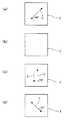
次に、図2(a)〜(d)を参照しながら、液晶表示素子1の光学仕様の一例について説明する。尚、図2(a)は図1のF偏光板3に、図2(b)は図1の位相差補償層5に、図2(c)は図1の液晶セル2に、図2(d)は図1のR偏光板4にそれぞれ対応する。また、この例では、位相差補償層5は、25℃で270nmのリタデーション値を有し、60℃でのリタデーション値が25℃でのリタデーション値より15%小さいものとしている。また、液晶セル2は、25℃で350nmのリタデーション値を有するものとしている。 Next, an example of the optical specifications of the liquid
図2(a)で、F偏光板3に示された矢印6は、F偏光板3の吸収軸の方向を示す。また、示された数字は設定角度を示し、水平方向を基準(0度)としている(図2(c)および(d)についても同様。)。同様に、図2(d)で、R偏光板4に示された矢印7は、R偏光板4の吸収軸の方向を示し、示された数字は設定角度であって、水平方向を基準(0度)としている。 In FIG. 2A, the arrow 6 indicated on the
また、図2(c)で、液晶セル2に示された矢印8は、液晶層を挟持する視認者側の基板における液晶配向処理の方向であり、具体的には、この基板上に設けられた垂直配向膜に対するラビングの方向を示す。同様に、液晶セル2に示された矢印9は、液晶層を挟持する反視認者側の基板における液晶配向処理の方向であり、具体的には、この基板上に設けられた垂直配向膜に対するラビングの方向を示す。 Further, in FIG. 2C, the arrow 8 shown in the
電圧を印加すると、液晶は、垂直配向の状態から、矢印8,9と平行な方向に配向を変化させる。そして、数字は、電圧印加時に液晶が略水平に配向したときの液晶の方位角を、水平方向を基準(0度)として示したものである。 When a voltage is applied, the liquid crystal changes its alignment from the vertical alignment state in a direction parallel to the
次に、液晶表示素子1の製造方法の一例について説明する。 Next, an example of a method for manufacturing the liquid
まず、一対のガラス基板の上に、所望の画像表示ができるようにパターニングされた電極層を設ける。電極層は、例えば、ITO(Indium Tin Oxide)電極とすることができる。 First, an electrode layer patterned so as to display a desired image is provided on a pair of glass substrates. The electrode layer can be, for example, an ITO (Indium Tin Oxide) electrode.
次いで、ガラス基板の上に、電極層を被覆するようにして絶縁膜を設ける。絶縁膜は、例えば、ゾル−ゲル法によって形成されたSiO2−TiO2からなる膜とすることができる。Next, an insulating film is provided on the glass substrate so as to cover the electrode layer. The insulating film can be, for example, a film made of SiO2 —TiO2 formed by a sol-gel method.
次に、液晶層において、液晶が初期配向状態として垂直に配向するように配向膜を形成する。例えば、JSR株式会社製の配向膜材料(商品名:JALS−2021)をフレキソ印刷法にて成膜し、基板を180℃で焼成することによって、厚さ600Å程度の配向膜を形成することができる。次いで、配向膜の表面にラビング処理を施して、上記した電界印加時の液晶の動作方向を定める。 Next, an alignment film is formed in the liquid crystal layer so that the liquid crystal is vertically aligned as an initial alignment state. For example, an alignment film having a thickness of about 600 mm can be formed by forming an alignment film material (trade name: JALS-2021) manufactured by JSR Corporation by flexographic printing and baking the substrate at 180 ° C. it can. Next, a rubbing process is performed on the surface of the alignment film to determine the operation direction of the liquid crystal when the electric field is applied.
次に、配向膜の形成工程までを終えた基板によって、液晶層を挟み込む。この際、例えば、樹脂スペーサを用いることによって、基板の間の距離(d)を一定に保つことができる。また、液晶層としては、例えば、屈折率異方性(Δn)が0.0875であるものを用いることができる。この場合、d=4μmとすると、液晶表示素子1のリタデーション(Δn・d)は350nmとなる。 Next, the liquid crystal layer is sandwiched between the substrates after the alignment film formation step. At this time, for example, the distance (d) between the substrates can be kept constant by using a resin spacer. As the liquid crystal layer, for example, a liquid crystal layer having a refractive index anisotropy (Δn) of 0.0875 can be used. In this case, when d = 4 μm, the retardation (Δn · d) of the liquid
次に位相差補償層を設ける。具体的には、液晶セル2の視認者側の面に一軸フィルムを配置する。この際、たとえば、高分子主骨格の側鎖に液晶分子を配置した材料を用いて形成した一軸フィルムを、温度補償機能を備えた位相差補償層として使用することができる。 Next, a retardation compensation layer is provided. Specifically, a uniaxial film is disposed on the viewer side surface of the
次に、偏光板3,4の設置を行う。具体的には、位相差補償層5が設けられた液晶セル2を挟持して、偏光板3,4がクロスニコル配置となるように貼り付ける。 Next, the
尚、詳細は図示されないが、本実施の形態における液晶表示素子1は、パッシブマトリクス構造である。すなわち、画像表示を構成する各画素部分には、TFT等のスイッチング素子は設けられておらず、電極層を用いたパッシブ駆動によって目的の画像が表示される。 Although not shown in detail, the liquid
次に、本実施の形態の液晶表示素子1において、室温(25℃)、40℃および60℃の各温度で発生する光漏れ現象を評価した結果の一例について述べる。 Next, an example of the result of evaluating the light leakage phenomenon that occurs at each temperature of room temperature (25 ° C.), 40 ° C., and 60 ° C. in the liquid
また、比較のために、温度補償性能を有しない位相差補償層を用いた以外は液晶表示素子1と同じ構造のVAモード液晶表示素子を用意し、同様の評価を行った。尚、比較例の位相差補償層としては、ポリカーボネート樹脂性の一軸延伸フィルムを用い、リタデーション値は液晶表示素子1と同じとした。 For comparison, a VA mode liquid crystal display element having the same structure as that of the liquid
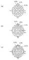
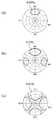
図3(a)〜(c)は、液晶表示素子1について、液晶の初期垂直配向時における黒表示での透過率の視角特性を示したものである。図3(a)は25℃での評価結果、図3(b)は40℃での評価結果、図3(c)は60℃での評価結果である。尚、評価は、シンテック株式会社製のシュミレーションソフト(LCD MASTER Ver.6.14)を用いて行っている。(以下、本明細書において同じ。) 3A to 3C show the viewing angle characteristics of the transmittance in the black display when the liquid
また、図4(a)〜(c)は、液晶表示素子1の比較例について、液晶の初期垂直配向時における黒表示での透過率の視角特性を示したものである。図4(a)は25℃での評価結果、図4(b)は40℃での評価結果、図4(c)は60℃での評価結果である。 4A to 4C show the viewing angle characteristics of transmittance in black display when the liquid
尚、図3(a)〜(c)および図4(a)〜(c)において、周囲の数字は方位角(表示面内の角度)であり、半径方向は0度から80度までの視角(表示面法線からの傾き角)を表す。また、図中の曲線に囲まれた領域は、透過率が0.1%、0.5%および1.0%である領域であって、それぞれ光漏れの起きている領域の位置および大きさを示している。したがって、これらの図を比較することによって、各温度における液晶表示素子1の光漏れの状況を評価することができる。 In FIGS. 3A to 3C and FIGS. 4A to 4C, the surrounding numbers are azimuth angles (angles in the display surface), and the radial direction is a viewing angle from 0 degrees to 80 degrees. (Inclination angle from display surface normal). In addition, the area surrounded by the curve in the figure is an area where the transmittance is 0.1%, 0.5% and 1.0%, and the position and size of the area where light leakage occurs, respectively. Is shown. Therefore, the situation of light leakage of the liquid
図4(a)〜(c)に示すように、液晶表示素子1の比較例では、透過率1.0%の領域は、25℃から40℃、さらに60℃と高温になるにしたがって広がっており、温度とともに光漏れが顕著となることが分かる。 As shown in FIGS. 4A to 4C, in the comparative example of the liquid
これに対して、図3(a)〜(c)に示すように、液晶表示素子1では、25℃、40℃および60℃の各温度条件で評価した透過率の視角特性に殆ど変化は見られない。このことは、温度補償機能を備えた温度補償型位相差補償層を用いることによって、広い温度域、特に高温域での斜め方向の光漏れを効果的に抑制できることを示している。 On the other hand, as shown in FIGS. 3A to 3C, the liquid
次に、本実施の形態における液晶表示素子1の別の例について述べる。 Next, another example of the liquid
位相差補償層5は、屈折率異方性を有するとともに、互いに直交するx軸、y軸および液晶セル2の厚み方向であるz軸の方向の主屈折率nx、nyおよびnzの間に、nxとnyは若干大きさが異なり且つnxとnyはnzより大きいという関係が成立する。The phase
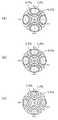
具体的には、液晶表示素子1における液晶層の厚みを用いて、RoをRo=(nx−ny)×液晶層厚、RthをRth=((nx+ny)/2−nz)×液晶層厚とそれぞれ定義し、Ro=50nm、Rth=250nmとする。図5(a)〜(c)は、このようなRo値とRth値を持つ液晶表示素子1について、液晶の初期垂直配向時における黒表示での透過率の視角特性を示したものである。図5(a)は25℃での評価結果、図5(b)は40℃での評価結果、図5(c)は60℃での評価結果である。Specifically, by using the thickness of the liquid crystal layer in the liquid
また、図6(a)〜(c)は、Ro=50nm、Rth=250nmである液晶表示素子1の比較例について、液晶の初期垂直配向時における黒表示での透過率の視角特性を示したものである。図6(a)は25℃での評価結果、図6(b)は40℃での評価結果、図6(c)は60℃での評価結果である。FIGS. 6A to 6C show the viewing angle characteristics of the transmittance in black display at the time of initial vertical alignment of the liquid crystal for the comparative example of the liquid
尚、図5(a)〜(c)および図6(a)〜(c)において、周囲の数字は方位角(表示面内の角度)であり、半径方向は0度から80度までの視角(表示面法線からの傾き角)を表す。また、図中の曲線に囲まれた領域は、透過率が0.05%である領域であって、それぞれ光漏れの起きている領域の位置および大きさを示している。したがって、これらの図を比較することによって、各温度における液晶表示素子1の光漏れの状況を評価することができる。 In FIGS. 5A to 5C and FIGS. 6A to 6C, the surrounding numbers are azimuth angles (angles within the display surface), and the radial direction is a viewing angle from 0 degrees to 80 degrees. (Inclination angle from display surface normal). In addition, the region surrounded by the curve in the figure is a region where the transmittance is 0.05%, and shows the position and size of the region where light leakage occurs. Therefore, the situation of light leakage of the liquid
図5(c)と図6(c)を比較すると、60℃において、液晶表示素子1における透過率0.05%の領域は比較例より小さい。したがって、本実施の形態によれば、高温時の光漏れが抑制されていることが分かる。このことは、温度補償機能を備えた温度補償型位相差補償層を用いることによって、広い温度域、特に高温域での斜め方向の光漏れを効果的に抑制できることを示している。 Comparing FIG. 5C and FIG. 6C, at 60 ° C., the area of the liquid
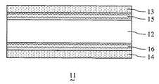
図7は、本実施の形態における他の例である液晶表示素子11の部分断面図である。 FIG. 7 is a partial cross-sectional view of a liquid crystal display element 11 which is another example of the present embodiment.
図7において、液晶表示素子11は、表面がそれぞれ垂直配向処理された一対の基板(図示せず)に挟持され、負の誘電異方性を有する液晶からなる液晶層を有する液晶セル12と、液晶セル12を挟持し、互いにクロスニコル配置された一対のF偏光板13およびR偏光板14と、F偏光板13と液晶セル12との間に設けられた位相差フィルム15と、R偏光板14と液晶セル12との間に設けられた位相差フィルム16とを有する。 In FIG. 7, a liquid crystal display element 11 includes a
液晶表示素子11では、位相差フィルム15および位相差フィルム16によって位相差補償層を構成している。位相差フィルム15,16の温度補償性能は、温度の上昇にしたがってリタデーション値が小さくなるものであるとする。具体的には、位相差フィルム15,16として、60℃でのリタデーション値が25℃でのリタデーション値より3%〜25%小さいものを用いる。これにより、広い温度域、特に高温域における液晶表示素子1の斜め方向の光漏れを効率良く抑制することができる。 In the liquid crystal display element 11, the
また、位相差フィルム15,16として、60℃でのリタデーション値が25℃でのリタデーション値より5%〜15%小さいものを使用することがより好ましい。これにより、広い温度域、特に高温域における液晶表示素子11の斜め方向の光漏れをより効率良く抑制することができる。 Moreover, it is more preferable to use the
さらに、液晶表示素子11においては、位相差フィルム15,16が屈折率異方性を有するとともに、互いに直交するx軸、y軸および液晶セル12の厚み方向であるz軸の方向の主屈折率nx、nyおよびnzの間に、nxとnyが等しく且つnxとnyはnzより大きい(nx=ny>nz)という関係が成立するものとすることができる。Further, in the liquid crystal display element 11, the
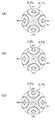
次に、図8(a)〜(e)を参照しながら、液晶表示素子11の光学仕様の一例について説明する。尚、図8(a)は図7のF偏光板13に、図8(b)は図7の位相差フィルム15に、図8(c)は図7の液晶セル12に、図8(d)は図7の位相差フィルム16に、図8(e)は図7のR偏光板14にそれぞれ対応する。また、この例では、位相差フィルム15,16は、25℃で135nmのリタデーション値を有し、60℃でのリタデーション値が25℃でのリタデーション値より15%小さいものとしている。また、液晶セル12は、25℃で350nmのリタデーション値を有するものとしている。 Next, an example of the optical specifications of the liquid crystal display element 11 will be described with reference to FIGS. 8A is the
図8(a)で、F偏光板13に示された矢印17は、F偏光板13の吸収軸の方向を示す。また、示された数字は設定角度を示し、水平方向を基準(0度)としている(図8(b)〜(e)についても同様。)。同様に、図8(e)で、R偏光板14に示された矢印18は、R偏光板14の吸収軸の方向を示し、示された数字は設定角度であって、水平方向を基準(0度)としている。 In FIG. 8A, the
また、図8(c)で、液晶セル12に示された矢印19は、液晶層を挟持する視認者側の基板における液晶配向処理の方向であり、具体的には、この基板上に設けられた垂直配向膜に対するラビングの方向を示す。同様に、液晶セル12に示された矢印20は、液晶層を挟持する反視認者側の基板における液晶配向処理の方向であり、具体的には、この基板上に設けられた垂直配向膜に対するラビングの方向を示す。 In FIG. 8C, the arrow 19 shown in the
電圧を印加すると、液晶は、垂直配向の状態から、矢印19,20と平行な方向に配向を変化させる。そして、数字は、電圧印加時に液晶が略水平に配向したときの液晶の方位角を、水平方向を基準(0度)として示したものである。 When a voltage is applied, the liquid crystal changes its orientation in the direction parallel to the
尚、本実施の形態における液晶表示素子11の製造方法については、位相差フィルムを2枚使用し、それぞれを液晶セル12の両面に配置して位相差補償層を形成すること以外は、すでに説明した液晶表示素子1の製造方法と同様である。 In addition, the manufacturing method of the liquid crystal display element 11 in the present embodiment has already been described except that two retardation films are used, and each is disposed on both surfaces of the
ここで、位相差フィルム15,16としては、液晶表示素子1の場合と同様に、一軸フィルムを用いることができる。具体的には、高分子主骨格の側鎖に液晶分子を配置した材料を用いて一軸フィルムを形成したものを、温度補償機能を有した位相差補償層として使用することができる。 Here, as the
尚、詳細は図示されないが、本実施の形態における液晶表示素子11は、パッシブマトリクス構造である。すなわち、画像表示を構成する各画素部分には、TFT等のスイッチング素子は設けられておらず、電極層を用いたパッシブ駆動によって目的の画像が表示される。 Although not shown in detail, the liquid crystal display element 11 in the present embodiment has a passive matrix structure. That is, each pixel portion constituting the image display is not provided with a switching element such as a TFT, and a target image is displayed by passive driving using an electrode layer.
次に、本実施の形態の液晶表示素子11において、室温(25℃)、40℃および60℃の各温度で発生する光漏れ現象を評価した結果の一例について述べる。 Next, an example of the result of evaluating the light leakage phenomenon generated at each temperature of room temperature (25 ° C.), 40 ° C., and 60 ° C. in the liquid crystal display element 11 of the present embodiment will be described.
また、比較のために、温度補償性能を有しない位相差フィルムを用いた以外は液晶表示素子11と同じ構造のVAモード液晶表示素子を用意し、同様の評価を行った。尚、比較例の位相差補償層としては、ポリカーボネート樹脂性の一軸延伸フィルムを用い、リタデーション値は液晶表示素子11と同じとした。 For comparison, a VA mode liquid crystal display element having the same structure as the liquid crystal display element 11 was prepared except that a retardation film having no temperature compensation performance was used, and the same evaluation was performed. In addition, as the retardation compensation layer of the comparative example, a polycarbonate resin uniaxially stretched film was used, and the retardation value was the same as that of the liquid crystal display element 11.
図9(a)〜(c)は、液晶表示素子11について、液晶の初期垂直配向時における黒表示での透過率の視角特性を示したものである。図9(a)は25℃での評価結果、図9(b)は40℃での評価結果、図9(c)は60℃での評価結果である。 FIGS. 9A to 9C show the viewing angle characteristics of the transmittance in black display when the liquid crystal display element 11 is in the initial vertical alignment of the liquid crystal. 9A shows an evaluation result at 25 ° C., FIG. 9B shows an evaluation result at 40 ° C., and FIG. 9C shows an evaluation result at 60 ° C.
また、図10(a)〜(c)は、液晶表示素子11の比較例について、液晶の初期垂直配向時における黒表示での透過率の視角特性を示したものである。図10(a)は25℃での評価結果、図10(b)は40℃での評価結果、図10(c)は60℃での評価結果である。 FIGS. 10A to 10C show the viewing angle characteristics of the transmittance in black display when the liquid crystal display element 11 is comparative, in the initial vertical alignment of the liquid crystal. 10A shows the evaluation result at 25 ° C., FIG. 10B shows the evaluation result at 40 ° C., and FIG. 10C shows the evaluation result at 60 ° C.
尚、図9(a)〜(c)および図10(a)〜(c)において、周囲の数字は方位角(表示面内の角度)であり、半径方向は0度から80度までの視角(表示面法線からの傾き角)を表す。また、図中の曲線に囲まれた領域は、透過率が0.1%および0.5%である領域であって、それぞれ光漏れの起きている領域の位置および大きさを示している。したがって、これらの図を比較することによって、各温度における液晶表示素子11の光漏れの状況を評価することができる。 In FIGS. 9A to 9C and FIGS. 10A to 10C, the surrounding numbers are azimuth angles (angles within the display surface), and the radial direction is a viewing angle from 0 degrees to 80 degrees. (Inclination angle from display surface normal). In addition, the area surrounded by the curve in the figure is an area where the transmittance is 0.1% and 0.5%, and indicates the position and size of the area where light leakage occurs, respectively. Therefore, the situation of light leakage of the liquid crystal display element 11 at each temperature can be evaluated by comparing these figures.
図10(a)〜(c)に示すように、液晶表示素子11の比較例において、25℃と40℃では透過率の高い領域の大きさに大差はない。温度が60℃になると、透過率0.5%の領域が明らかに大きくなっている。 As shown in FIGS. 10A to 10C, in the comparative example of the liquid crystal display element 11, there is no great difference in the size of the high transmittance region at 25 ° C. and 40 ° C. When the temperature reaches 60 ° C., the region with a transmittance of 0.5% clearly increases.
これに対して、図9(a)〜(c)に示すように、液晶表示素子11では、25℃と40℃では透過率の高い領域の大きさに大差はない。温度が60℃になっても同様であり、透過率の視角特性全体では25℃と比較して高温になっても大きな変化はない。
したがって、液晶表示素子11では、特に高温の60℃における透過率0.5%の領域が、比較例に比べ明確に狭くなっていることが分かる。すなわち、高温条件下で、液晶の初期垂直配向時における黒表示での透過率の視角特性が向上していることが分かる。このことは、温度補償機能を備えた一対の位相差フィルムを用いることによって、広い温度域、特に高温域での斜め方向の光漏れを効果的に抑制できることを示している。On the other hand, as shown in FIGS. 9A to 9C, in the liquid crystal display element 11, there is no great difference in the size of the high transmittance region at 25 ° C. and 40 ° C. The same is true when the temperature reaches 60 ° C., and the entire viewing angle characteristic of the transmittance does not change greatly even when the temperature becomes higher than 25 ° C.
Therefore, it can be seen that in the liquid crystal display element 11, the region having a transmittance of 0.5% particularly at a high temperature of 60 ° C. is clearly narrower than the comparative example. That is, it can be seen that the viewing angle characteristics of the transmittance in black display during the initial vertical alignment of the liquid crystal are improved under high temperature conditions. This has shown that the light leakage of the diagonal direction in a wide temperature range, especially a high temperature range can be effectively suppressed by using a pair of retardation film provided with the temperature compensation function.
次に、本実施の形態における液晶表示素子11の別の例について述べる。 Next, another example of the liquid crystal display element 11 in the present embodiment will be described.
位相差補償層を構成する位相差フィルム15,16は、それぞれ屈折率異方性を有するとともに、互いに直交するx軸、y軸および液晶セル12の厚み方向であるz軸の方向の主屈折率nx、nyおよびnzの間に、nxとnyは若干大きさが異なり且つnxとnyはnzより大きいという関係が成立する。The
具体的には、液晶表示素子11における液晶層の厚みを用いて、RoをRo=(nx−ny)×液晶層厚、RthをRth=((nx+ny)/2−nz)×液晶層厚とそれぞれ定義し、Ro=40nm、Rth=130nmとする。図11(a)〜(c)は、このようなRo値とRth値を持つ液晶表示素子1について、液晶の初期垂直配向時における黒表示での透過率の視角特性を示したものである。図11(a)は25℃での評価結果、図11(b)は40℃での評価結果、図11(c)は60℃での評価結果である。Specifically, by using the thickness of the liquid crystal layer in the liquid crystal display device 11, theR o R o = (n x -n y) × liquid crystal layerthickness, theR th R th = ((n x + n y) / 2-nz ) × liquid crystal layer thickness, and Ro = 40 nm and Rth = 130 nm. FIGS. 11A to 11C show the viewing angle characteristics of transmittance in black display when the liquid
また、図12(a)〜(c)は、位相差フィルム15,16がそれぞれRo=40nm、Rth=130nmである液晶表示素子11の比較例について、液晶の初期垂直配向時における黒表示での透過率の視角特性を示したものである。図12(a)は25℃での評価結果、図12(b)は40℃での評価結果、図12(c)は60℃での評価結果である。FIGS. 12A to 12C show black display at the time of initial vertical alignment of the liquid crystal for the comparative example of the liquid crystal display element 11 in which the
尚、図11(a)〜(c)および図12(a)〜(c)において、周囲の数字は方位角(表示面内の角度)であり、半径方向は0度から80度までの視角(表示面法線からの傾き角)を表す。また、図中の曲線に囲まれた領域は、透過率が0.02%である領域であって、それぞれ光漏れの起きている領域の位置および大きさを示している。したがって、これらの図を比較することによって、各温度における液晶表示素子11の光漏れの状況を評価することができる。 In FIGS. 11A to 11C and FIGS. 12A to 12C, the surrounding numbers are azimuths (angles within the display surface), and the radial direction is a viewing angle from 0 degrees to 80 degrees. (Inclination angle from display surface normal). Also, the area surrounded by the curve in the figure is an area where the transmittance is 0.02%, and shows the position and size of the area where light leakage occurs. Therefore, the situation of light leakage of the liquid crystal display element 11 at each temperature can be evaluated by comparing these figures.
図11(c)と図12(c)を比較すると、液晶表示素子11における透過率0.02%の領域は、40℃および60℃において比較例より明らかに小さい。したがって、本実施の形態によれば、25℃から40℃、さらには60℃と高温になった場合に、比較例と比べて光漏れを抑制できることが分かる。すなわち、高温条件下で、液晶の初期垂直配向時における黒表示での透過率の視角特性が向上していることが分かる。このことは、温度補償機能を備えた温度補償型位相差補償層を用いることによって、広い温度域、特に高温域での斜め方向の光漏れを効果的に抑制できることを示している。 Comparing FIG. 11C and FIG. 12C, the region of the transmittance 0.02% in the liquid crystal display element 11 is clearly smaller than the comparative example at 40 ° C. and 60 ° C. Therefore, according to the present embodiment, it can be seen that light leakage can be suppressed compared to the comparative example when the temperature is increased from 25 ° C. to 40 ° C., and further to 60 ° C. That is, it can be seen that the viewing angle characteristics of the transmittance in black display during the initial vertical alignment of the liquid crystal are improved under high temperature conditions. This indicates that by using a temperature compensation type phase difference compensation layer having a temperature compensation function, light leakage in an oblique direction in a wide temperature range, particularly in a high temperature range, can be effectively suppressed.
実施の形態2.
図13は、本実施の形態における液晶表示素子31の部分断面図である。尚、液晶表示素子31は、VAモード液晶表示素子であるとする。
FIG. 13 is a partial cross-sectional view of the liquid
図13において、液晶表示素子31は、表面がそれぞれ垂直配向処理された一対の基板(図示せず)に挟持され、負の誘電異方性を有する液晶からなる液晶層を有する液晶セル32と、液晶セル32を挟持し、互いにクロスニコル配置された一対のF偏光板33およびR偏光板34と、F偏光板33と液晶セル32との間に設けられた位相差フィルム35と、R偏光板34と液晶セル32との間に設けられた位相差フィルム36とを有する。 In FIG. 13, a liquid
液晶表示素子31では、位相差フィルム35および位相差フィルム36によって位相差補償層を構成している。位相差フィルム35,36の温度補償性能は、温度の上昇にしたがってリタデーション値が小さくなるものであるとする。具体的には、位相差フィルム35,36として、60℃でのリタデーション値が25℃でのリタデーション値より3%〜25%小さいものを用いる。これにより、広い温度域、特に高温域における液晶表示素子31の斜め方向の光漏れを効率良く抑制することができる。 In the liquid
また、位相差フィルム35,36として、60℃でのリタデーション値が25℃でのリタデーション値より5%〜15%小さいものを使用することがより好ましい。これにより、広い温度域、特に高温域における液晶表示素子31の斜め方向の光漏れをより効率良く抑制することができる。 Moreover, it is more preferable to use a
さらに、液晶表示素子31においては、位相差フィルム35,36が屈折率異方性を有するとともに、互いに直交するx軸、y軸および液晶セル32の厚み方向であるz軸の方向の主屈折率nx、nyおよびnzの間に、nyとnzが等しく且つnxはnyとnzより大きい(nx>ny=nz)という関係が成立するものとすることができる。Further, in the liquid
ここで、位相差フィルム35の主屈折率をnx1、ny1およびnz1とし、位相差フィルム36の主屈折率をnx2、ny2およびnz2とし、さらに、位相差補償層の主屈折率をnx′とny′およびnz′とすると、次式の関係が成立する。Here, the main refractive index of the
nx′=(nx1+ny2)/2
ny′=(ny1+nx2)/2
nz′=nz1=nz2
nx′≒ny′>nz′nx '= (nx1 +ny2 ) / 2
ny ′ = (ny1 + nx2 ) / 2
nz ′ = nz1 = nz2
nx '≈ny '> nz '
次に、図14(a)〜(e)を参照しながら、液晶表示素子31の光学仕様の一例について説明する。尚、図14(a)は図13のF偏光板33に、図14(b)は図13の位相差フィルム35に、図14(c)は図13の液晶セル32に、図14(d)は図13の位相差フィルム36に、図14(e)は図13のR偏光板34にそれぞれ対応する。また、この例では、位相差フィルム35,36は、25℃で105nmのリタデーション値を有し、60℃でのリタデーション値が25℃でのリタデーション値より15%小さいものとしている。また、液晶セル32は、25℃で350nmのリタデーション値を有するものとしている。 Next, an example of the optical specifications of the liquid
図14(a)で、F偏光板33に示された矢印37は、F偏光板33の吸収軸の方向を示す。また、示された数字は設定角度を示し、水平方向を基準(0度)としている(図14(b)〜(e)についても同様。)。同様に、図14(e)で、R偏光板34に示された矢印38は、R偏光板34の吸収軸の方向を示し、示された数字は設定角度であって、水平方向を基準(0度)としている。 In FIG. 14A, an
また、図14(c)で、液晶セル32に示された矢印39は、液晶層を挟持する視認者側の基板における液晶配向処理の方向であり、具体的には、この基板上に設けられた垂直配向膜に対するラビングの方向を示す。同様に、液晶セル32に示された矢印40は、液晶層を挟持する反視認者側の基板における液晶配向処理の方向であり、具体的には、この基板上に設けられた垂直配向膜に対するラビングの方向を示す。 In FIG. 14C, an arrow 39 shown in the
さらに、図14(b)および(d)における矢印41,42は、それぞれ主屈折率が最大となるnx方向、すなわち位相差フィルム35,36の遅相軸方向を示している。よって、位相差補償層を構成する2つの層については、これら2つの層の内の一方の層の遅相軸と、他方の層の進相軸とが一致するよう配置されている。Further,
電圧を印加すると、液晶は、垂直配向の状態から、矢印39,40と平行な方向に配向を変化させる。そして、数字は、電圧印加時に液晶が略水平に配向したときの液晶の方位角を、水平方向を基準(0度)として示したものである。 When a voltage is applied, the liquid crystal changes its orientation in the direction parallel to the
尚、本実施の形態における液晶表示素子31の製造方法については、位相差フィルムを2枚使用し、それぞれを液晶セル32の両面に配置して位相差補償層を形成すること以外は、実施の形態1で説明した液晶表示素子1の製造方法と同様である。 In addition, about the manufacturing method of the liquid
ここで、位相差フィルム35,36としては、液晶表示素子1の場合と同様に、一軸フィルムを用いることができる。具体的には、高分子主骨格の側鎖に液晶分子を配置した材料を用いて一軸フィルムを形成したものを、温度補償機能を有した位相差補償層として使用することができる。 Here, as the
尚、詳細は図示されないが、本実施の形態における液晶表示素子31は、パッシブマトリクス構造である。すなわち、画像表示を構成する各画素部分には、TFT等のスイッチング素子は設けられておらず、電極層を用いたパッシブ駆動によって目的の画像が表示される。 Although not shown in detail, the liquid
次に、本実施の形態の液晶表示素子31において、室温(25℃)、40℃および60℃の各温度で発生する光漏れ現象を評価した結果の一例について述べる。 Next, an example of the result of evaluating the light leakage phenomenon that occurs at room temperature (25 ° C.), 40 ° C., and 60 ° C. in the liquid
また、比較のために、温度補償性能を有しない位相差フィルムを用いた以外は液晶表示素子31と同じ構造のVAモード液晶表示素子を用意し、同様の評価を行った。尚、比較例の位相差補償層としては、ポリカーボネート樹脂性の一軸延伸フィルムを用い、リタデーション値は液晶表示素子31と同じとした。 For comparison, a VA mode liquid crystal display element having the same structure as the liquid
図15(a)〜(c)は、液晶表示素子31について、液晶の初期垂直配向時における黒表示での透過率の視角特性を示したものである。図15(a)は25℃での評価結果、図15(b)は40℃での評価結果、図15(c)は60℃での評価結果である。 FIGS. 15A to 15C show the viewing angle characteristics of the transmittance in black display when the liquid
また、図16(a)〜(c)は、液晶表示素子31の比較例について、液晶の初期垂直配向時における黒表示での透過率の視角特性を示したものである。図16(a)は25℃での評価結果、図16(b)は40℃での評価結果、図16(c)は60℃での評価結果である。 FIGS. 16A to 16C show the viewing angle characteristics of transmittance in black display when the liquid
尚、図15(a)〜(c)および図16(a)〜(c)において、周囲の数字は方位角(表示面内の角度)であり、半径方向は0度から80度までの視角(表示面法線からの傾き角)を表す。また、図中の曲線に囲まれた領域は、透過率が0.1%、0.5%および1.0%である領域であって、それぞれ光漏れの起きている領域の位置および大きさを示している。したがって、これらの図を比較することによって、各温度における液晶表示素子1の光漏れの状況を評価することができる。 In FIGS. 15A to 15C and FIGS. 16A to 16C, the surrounding numbers are azimuth angles (angles within the display surface), and the radial direction is a viewing angle from 0 degrees to 80 degrees. (Inclination angle from display surface normal). In addition, the area surrounded by the curve in the figure is an area where the transmittance is 0.1%, 0.5% and 1.0%, and the position and size of the area where light leakage occurs, respectively. Is shown. Therefore, the situation of light leakage of the liquid
図16(a)〜(c)に示すように、液晶表示素子31の比較例において、25℃と40℃では透過率の高い領域の大きさに大差はない。温度が60℃になると、透過率1.0%の領域が若干狭くなっているものの、透過率の視角特性全体では25℃と比較しても大きな変化はない。 As shown in FIGS. 16A to 16C, in the comparative example of the liquid
これに対して、図15(a)〜(c)に示すように、液晶表示素子31では、25℃での透過率の視角特性と比べ、特に高温の60℃における透過率0.5%および1.0%の領域が明確に狭くなっていることが分かる。すなわち、高温条件下で、液晶の初期垂直配向時における黒表示での透過率の視角特性が向上していることが分かる。このことは、温度補償機能を備えた一対の位相差フィルムを用いることによって、広い温度域、特に高温域での斜め方向の光漏れを効果的に抑制できることを示している。 On the other hand, as shown in FIGS. 15A to 15C, the liquid
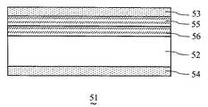
図17は、本実施の形態における別の例である液晶表示素子51の部分断面図である。 FIG. 17 is a partial cross-sectional view of a liquid
図17において、液晶表示素子51は、表面がそれぞれ垂直配向処理された一対の基板(図示せず)に挟持され、負の誘電異方性を有する液晶からなる液晶層を有する液晶セル52と、液晶セル52を挟持し、互いにクロスニコル配置された一対のF偏光板53およびR偏光板54と、F偏光板53と液晶セル52との間に設けられた位相差フィルム55
,56とを有する。In FIG. 17, a liquid
, 56.
液晶表示素子51では、位相差フィルム55および位相差フィルム56によって位相差補償層を構成している。位相差フィルム55,56の温度補償性能は、温度の上昇にしたがってリタデーション値が小さくなるものであるとする。具体的には、位相差フィルム55,56として、60℃でのリタデーション値が25℃でのリタデーション値より3%〜25%小さいものを用いる。これにより、広い温度域、特に高温域における液晶表示素子51の斜め方向の光漏れを効率良く抑制することができる。 In the liquid
また、位相差フィルム55,56として、60℃でのリタデーション値が25℃でのリタデーション値より5%〜15%小さいものを使用することがより好ましい。これにより、広い温度域、特に高温域における液晶表示素子51の斜め方向の光漏れをより効率良く抑制することができる。 Moreover, it is more preferable to use a
さらに、液晶表示素子51においては、位相差フィルム55,56が屈折率異方性を有するとともに、互いに直交するx軸、y軸および液晶セル52の厚み方向であるz軸の方向の主屈折率nx、nyおよびnzの間に、nyとnzが等しく且つnxはnyとnzより大きい(nx>ny=nz)という関係が成立するものとすることができる。Further, in the liquid
ここで、位相差フィルム55の主屈折率をnx1、ny1およびnz1とし、位相差フィルム56の主屈折率をnx2、ny2およびnz2とし、さらに、位相差補償層の主屈折率をnx′とny′およびnz′とすると、次式の関係が成立する。Here, the main refractive index of the
nx′=(nx1+ny2)/2
ny′=(ny1+nx2)/2
nz′=nz1=nz2
nx′≒ny′>nz′nx '= (nx1 +ny2 ) / 2
ny ′ = (ny1 + nx2 ) / 2
nz ′ = nz1 = nz2
nx '≈ny '> nz '
次に、図18(a)〜(e)を参照しながら、液晶表示素子51の光学仕様の一例について説明する。尚、図18(a)は図17のF偏光板53に、図18(b)は図17の位相差フィルム55に、図18(c)は図17の位相差フィルム56に、図18(d)は図17の液晶セル52に、図18(e)は図17のR偏光板54にそれぞれ対応する。また、この例では、位相差フィルム55,56は、25℃で105nmのリタデーション値を有し、60℃でのリタデーション値が25℃でのリタデーション値より15%小さいものとしている。また、液晶セル52は、25℃で350nmのリタデーション値を有するものとしている。 Next, an example of optical specifications of the liquid
図18(a)で、F偏光板53に示された矢印57は、F偏光板53の吸収軸の方向を示す。また、示された数字は設定角度を示し、水平方向を基準(0度)としている(図18(b)〜(e)についても同様。)。同様に、図18(e)で、R偏光板54に示された矢印58は、R偏光板54の吸収軸の方向を示し、示された数字は設定角度であって、水平方向を基準(0度)としている。 In FIG. 18A, an
また、図18(d)で、液晶セル52に示された矢印59は、液晶層を挟持する視認者側の基板における液晶配向処理の方向であり、具体的には、この基板上に設けられた垂直配向膜に対するラビングの方向を示す。同様に、液晶セル52に示された矢印60は、液晶層を挟持する反視認者側の基板における液晶配向処理の方向であり、具体的には、この基板上に設けられた垂直配向膜に対するラビングの方向を示す。 In FIG. 18D, an arrow 59 shown in the
さらに、図18(b)および(c)における矢印61,62は、それぞれ主屈折率が最大となるnx方向、すなわち位相差フィルム55,56の遅相軸方向を示している。よって、位相差補償層を構成する2つの層については、これら2つの層の内の一方の層の遅相軸と、他方の層の進相軸とが一致するよう配置されている。Further,
電圧を印加すると、液晶は、垂直配向の状態から、矢印59,60と平行な方向に配向を変化させる。そして、数字は、電圧印加時に液晶が略水平に配向したときの液晶の方位角を、水平方向を基準(0度)として示したものである。 When a voltage is applied, the liquid crystal changes its orientation in the direction parallel to the arrows 59 and 60 from the vertically oriented state. The numbers indicate the azimuth angle of the liquid crystal when the liquid crystal is aligned substantially horizontally when a voltage is applied, with the horizontal direction as a reference (0 degree).
尚、本実施の形態における液晶表示素子51の製造方法については、位相差フィルムを2枚使用し、それぞれを液晶セル52とF板偏光板53との間に配置して位相差補償層を形成すること以外は、実施の形態1で説明した液晶表示素子1の製造方法と同様である。 In addition, about the manufacturing method of the liquid
ここで、位相差フィルム55,56としては、液晶表示素子1の場合と同様に、一軸フィルムを用いることができる。具体的には、高分子主骨格の側鎖に液晶分子を配置した材料を用いて一軸フィルムを形成したものを、温度補償機能を有した位相差補償層として使用することができる。 Here, as the
尚、詳細は図示されないが、本実施の形態における液晶表示素子51は、パッシブマトリクス構造である。すなわち、画像表示を構成する各画素部分には、TFT等のスイッチング素子は設けられておらず、電極層を用いたパッシブ駆動によって目的の画像が表示される。 Although not shown in detail, the liquid
次に、本実施の形態の液晶表示素子51において、室温(25℃)、40℃および60℃の各温度で発生する光漏れ現象を評価した結果の一例について述べる。 Next, an example of the result of evaluating the light leakage phenomenon that occurs at room temperature (25 ° C.), 40 ° C., and 60 ° C. in the liquid
また、比較のために、温度補償性能を有しない位相差フィルムを用いた以外は液晶表示素子51と同じ構造のVAモード液晶表示素子を用意し、同様の評価を行った。尚、比較例の位相差補償層としては、ポリカーボネート樹脂性の一軸延伸フィルムを用い、リタデーション値は液晶表示素子51と同じとした。 For comparison, a VA mode liquid crystal display element having the same structure as the liquid
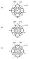
図19(a)〜(c)は、液晶表示素子51について、液晶の初期垂直配向時における黒表示での透過率の視角特性を示したものである。図19(a)は25℃での評価結果、図19(b)は40℃での評価結果、図19(c)は60℃での評価結果である。 FIGS. 19A to 19C show the viewing angle characteristics of the transmittance in black display when the liquid
また、図20(a)〜(c)は、液晶表示素子51の比較例について、液晶の初期垂直配向時における黒表示での透過率の視角特性を示したものである。図20(a)は25℃での評価結果、図20(b)は40℃での評価結果、図20(c)は60℃での評価結果である。 20A to 20C show viewing angle characteristics of transmittance in black display when the liquid
尚、図19(a)〜(c)および図20(a)〜(c)において、周囲の数字は方位角(表示面内の角度)であり、半径方向は0度から80度までの視角(表示面法線からの傾き角)を表す。また、図中の曲線に囲まれた領域は、透過率が0.1%、0.5%および1.0%である領域であって、それぞれ光漏れの起きている領域の位置および大きさを示している。したがって、これらの図を比較することによって、各温度における液晶表示素子1の光漏れの状況を評価することができる。 In FIGS. 19A to 19C and FIGS. 20A to 20C, the surrounding numbers are azimuths (angles in the display surface), and the radial direction is a viewing angle from 0 degrees to 80 degrees. (Inclination angle from display surface normal). In addition, the area surrounded by the curve in the figure is an area where the transmittance is 0.1%, 0.5% and 1.0%, and the position and size of the area where light leakage occurs, respectively. Is shown. Therefore, the situation of light leakage of the liquid
図20(a)〜(c)に示すように、液晶表示素子51の比較例において、25℃と40℃では透過率の高い領域の大きさに大差はない。温度が60℃になると、透過率1.0%の領域が若干狭くなっているものの、透過率の視角特性全体では25℃と比較しても大きな変化はない。 As shown in FIGS. 20A to 20C, in the comparative example of the liquid
これに対して、図19(a)〜(c)に示すように、液晶表示素子51では、25℃での透過率の視角特性と比べ、特に高温の60℃における透過率0.5%および1.0%の領域が明確に狭くなっていることが分かる。すなわち、高温条件下で、液晶の初期垂直配向時における黒表示での透過率の視角特性が向上していることが分かる。このことは、温度補償機能を備えた一対の位相差フィルムを用いることによって、広い温度域、特に高温域での斜め方向の光漏れを効果的に抑制できることを示している。 On the other hand, as shown in FIGS. 19A to 19C, the liquid
実施の形態3.
図21は、本実施の形態における液晶表示素子71の部分断面図である。尚、液晶表示素子71は、VAモード液晶表示素子であるとする。
FIG. 21 is a partial cross-sectional view of the liquid
図21において、液晶表示素子71は、表面がそれぞれ垂直配向処理された一対の基板(図示せず)に挟持され、負の誘電異方性を有する液晶からなる液晶層を有する液晶セル72と、液晶セル72を挟持し、互いにクロスニコル配置された一対のF偏光板73およびR偏光板74と、F偏光板73と液晶セル72との間に設けられた位相差フィルム75と、R偏光板74と液晶セル72との間に設けられた位相差フィルム76とを有する。 In FIG. 21, a liquid
液晶表示素子71では、位相差フィルム75および位相差フィルム76によって位相差補償層を構成している。位相差フィルム75,76の温度補償性能は、温度の上昇にしたがってリタデーション値が小さくなるものであるとする。具体的には、位相差フィルム75,76として、60℃でのリタデーション値が25℃でのリタデーション値より3%〜25%小さいものを用いる。これにより、広い温度域、特に高温域における液晶表示素子71の斜め方向の光漏れを効率良く抑制することができる。 In the liquid
また、位相差フィルム75,76として、60℃でのリタデーション値が25℃でのリタデーション値より5%〜15%小さいものを使用することがより好ましい。これにより、広い温度域、特に高温域における液晶表示素子71の斜め方向の光漏れをより効率良く抑制することができる。 Moreover, it is more preferable to use a
位相差フィルム75は、屈折率異方性を有するとともに、互いに直交するx軸、y軸および液晶セル72の厚み方向であるz軸の方向の主屈折率nx、nyおよびnzの間に、nxとnyが等しく且つnxとnyはnzより大きい(nx=ny>nz)という関係が成立するものとすることができる。The
一方、位相差フィルム76は、屈折率異方性を有するとともに、互いに直交するx軸、y軸および液晶セル72の厚み方向であるz軸の方向の主屈折率nx、nyおよびnzの間に、nyとnzが等しく且つnxはnyとnzより大きい(nx>ny=nz)という関係が成立するものとすることができる。On the other hand, the
次に、図22(a)〜(e)を参照しながら、液晶表示素子71の光学仕様の一例について説明する。尚、図22(a)は図20のF偏光板73に、図22(b)は図20の位相差フィルム75に、図22(c)は図20の液晶セル72に、図22(d)は図20の位相差フィルム76に、図22(e)は図20のR偏光板74にそれぞれ対応する。 Next, an example of the optical specifications of the liquid
また、この例では、位相差フィルム75は、25℃でのリタデーション値についてRth=200nmの値を有し、60℃でのリタデーション値が25℃でのリタデーション値より15%小さいものとしている。また、この例では、位相差フィルム76は、25℃でのリタデーション値についてRo=110nmの値を有し、60℃でのリタデーション値が25℃でのリタデーション値より15%小さいものとしている。In this example, the
尚、RthおよびRoの定義については上記した例と同様であり、液晶表示素子71における液晶層の厚みを用いて、RoをRo=(nx−ny)×液晶層厚、RthをRth=((nx+ny)/2−nz)×液晶層厚と定義している。また、液晶セル72は、25℃で350nmのリタデーション値を有するものとしている。Notethat the definition ofR th andR o are the same as in the example described above, with the thickness of the liquid crystal layer in the liquid
図22(a)で、F偏光板73に示された矢印77は、F偏光板73の吸収軸の方向を示す。また、示された数字は設定角度を示し、水平方向を基準(0度)としている(図22(b)〜(e)についても同様。)。同様に、図22(e)で、R偏光板74に示された矢印78は、R偏光板74の吸収軸の方向を示し、示された数字は設定角度であって、水平方向を基準(0度)としている。 In FIG. 22A, the
また、図22(c)で、液晶セル72に示された矢印79は、液晶層を挟持する視認者側の基板における液晶配向処理の方向であり、具体的には、この基板上に設けられた垂直配向膜に対するラビングの方向を示す。同様に、液晶セル72に示された矢印80は、液晶層を挟持する反視認者側の基板における液晶配向処理の方向であり、具体的には、この基板上に設けられた垂直配向膜に対するラビングの方向を示す。 In FIG. 22C, an
さらに、図22(d)における矢印81は、それぞれ主屈折率が最大となるnx方向、すなわち位相差フィルム76の遅相軸方向を示している。Further,
電圧を印加すると、液晶は、垂直配向の状態から、矢印79,80と平行な方向に配向を変化させる。そして、数字は、電圧印加時に液晶が略水平に配向したときの液晶の方位角を、水平方向を基準(0度)として示したものである。 When a voltage is applied, the liquid crystal changes its orientation in the direction parallel to the
尚、本実施の形態における液晶表示素子71の製造方法については、位相差フィルムを2枚使用し、それぞれを液晶セル72の両面に配置して位相差補償層を形成すること以外は、実施の形態1で説明した液晶表示素子1の製造方法と同様である。 In addition, about the manufacturing method of the liquid
ここで、位相差フィルム75,76としては、液晶表示素子1の場合と同様に、一軸フィルムを用いることができる。具体的には、高分子主骨格の側鎖に液晶分子を配置した材料を用いて一軸フィルムを形成したものを、温度補償機能を有した位相差補償層として使用することができる。 Here, as the
尚、詳細は図示されないが、本実施の形態における液晶表示素子71は、パッシブマトリクス構造である。すなわち、画像表示を構成する各画素部分には、TFT等のスイッチング素子は設けられておらず、電極層を用いたパッシブ駆動によって目的の画像が表示される。 Although not shown in detail, the liquid
次に、本実施の形態の液晶表示素子31において、室温(25℃)、40℃および60℃の各温度で発生する光漏れ現象を評価した結果の一例について述べる。 Next, an example of the result of evaluating the light leakage phenomenon that occurs at room temperature (25 ° C.), 40 ° C., and 60 ° C. in the liquid
また、比較のために、温度補償性能を有しない位相差フィルムを用いた以外は液晶表示素子71と同じ構造のVAモード液晶表示素子を用意し、同様の評価を行った。尚、比較例の位相差補償層としては、ポリカーボネート樹脂性の一軸延伸フィルムを用い、リタデーション値は液晶表示素子71と同じとした。 For comparison, a VA mode liquid crystal display element having the same structure as the liquid
図23(a)〜(c)は、液晶表示素子71について、液晶の初期垂直配向時における黒表示での透過率の視角特性を示したものである。図23(a)は25℃での評価結果、図23(b)は40℃での評価結果、図23(c)は60℃での評価結果である。 FIGS. 23A to 23C show the viewing angle characteristics of the transmittance in black display when the liquid
また、図24(a)〜(c)は、液晶表示素子71の比較例について、液晶の初期垂直配向時における黒表示での透過率の視角特性を示したものである。図24(a)は25℃での評価結果、図24(b)は40℃での評価結果、図24(c)は60℃での評価結果である。 FIGS. 24A to 24C show the viewing angle characteristics of the transmittance in black display when the liquid
尚、図23(a)〜(c)および図24(a)〜(c)において、周囲の数字は方位角(表示面内の角度)であり、半径方向は0度から80度までの視角(表示面法線からの傾き角)を表す。また、図中の曲線に囲まれた領域は、透過率が0.03%である領域であって、それぞれ光漏れの起きている領域の位置および大きさを示している。したがって、これらの図を比較することによって、各温度における液晶表示素子71の光漏れの状況を評価することができる。 In FIGS. 23 (a) to 23 (c) and FIGS. 24 (a) to 24 (c), the surrounding numbers are azimuths (angles within the display surface), and the radial direction is a viewing angle from 0 degrees to 80 degrees. (Inclination angle from display surface normal). In addition, the region surrounded by the curve in the figure is a region where the transmittance is 0.03%, and indicates the position and size of the region where light leakage occurs. Therefore, by comparing these figures, the state of light leakage of the liquid
図24(a)〜(c)に示すように、液晶表示素子71の比較例において、25℃と40℃では透過率の高い領域の大きさに大差はない。しかし、温度が60℃になると、透過率0.03%の領域が顕著に広がっており、光漏れが顕著となって透過率の視角特性全体では25℃と比較しても大きく劣っている。 As shown in FIGS. 24A to 24C, in the comparative example of the liquid
これに対して、図23(a)〜(c)に示すように、液晶表示素子71では、25℃での透過率の視角特性と比べ、40℃、およびより高温の60℃における透過率0.03%の領域は大きな差はない。すなわち、60℃においても透過率0.03%領域が顕著に広がるということは無い。このことは、温度補償機能を備えた一対の位相差フィルムを用いることによって、広い温度域、特に高温域での斜め方向の光漏れを効果的に抑制できることを示している。 On the other hand, as shown in FIGS. 23A to 23C, the liquid
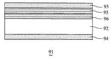
図25は、本実施の形態における別の例である液晶表示素子91の部分断面図である。 FIG. 25 is a partial cross-sectional view of a liquid
図25において、液晶表示素子91は、表面がそれぞれ垂直配向処理された一対の基板(図示せず)に挟持され、負の誘電異方性を有する液晶からなる液晶層を有する液晶セル92と、液晶セル92を挟持し、互いにクロスニコル配置された一対のF偏光板93およびR偏光板94と、F偏光板93と液晶セル92との間に設けられた位相差フィルム95
,96とを有する。In FIG. 25, a liquid
, 96.
液晶表示素子91では、位相差フィルム95および位相差フィルム96によって位相差補償層を構成している。位相差フィルム95,96の温度補償性能は、温度の上昇にしたがってリタデーション値が小さくなるものであるとする。具体的には、位相差フィルム95,96として、60℃でのリタデーション値が25℃でのリタデーション値より3%〜25%小さいものを用いる。これにより、広い温度域、特に高温域における液晶表示素子91の斜め方向の光漏れを効率良く抑制することができる。 In the liquid
また、位相差フィルム95,96として、60℃でのリタデーション値が25℃でのリタデーション値より5%〜15%小さいものを使用することがより好ましい。これにより、広い温度域、特に高温域における液晶表示素子91の斜め方向の光漏れをより効率良く抑制することができる。 Further, it is more preferable to use a
位相差フィルム95は、屈折率異方性を有するとともに、互いに直交するx軸、y軸および液晶セル92の厚み方向であるz軸の方向の主屈折率nx、nyおよびnzの間に、nxとnyが等しく且つnxとnyはnzより大きい(nx=ny>nz)という関係が成立するものとすることができる。The
一方、位相差フィルム96は、屈折率異方性を有するとともに、互いに直交するx軸、y軸および液晶セル92の厚み方向であるz軸の方向の主屈折率nx、nyおよびnzの間に、nyとnzが等しく且つnxはnyとnzより大きい(nx>ny=nz)という関係が成立するものとすることができる。On the other hand, the
次に、図26(a)〜(e)を参照しながら、液晶表示素子91の光学仕様の一例について説明する。尚、図26(a)は図25のF偏光板93に、図26(b)は図25の位相差フィルム95に、図26(c)は図25の位相差フィルム96に、図26(d)は図25の液晶セル92に、図26(e)は図25のR偏光板94にそれぞれ対応する。 Next, an example of the optical specifications of the liquid
また、この例では、位相差フィルム95は、25℃でのリタデーション値についてRth=200nmの値を有し、60℃でのリタデーション値が25℃でのリタデーション値より15%小さいものとしている。また、この例では、位相差フィルム96は、25℃でのリタデーション値についてRo=110nmの値を有し、60℃でのリタデーション値が25℃でのリタデーション値より15%小さいものとしている。In this example, the
尚、RthおよびRoの定義については上記した例と同様であり、液晶表示素子91における液晶層の厚みを用いて、RoをRo=(nx−ny)×液晶層厚、RthをRth=((nx+ny)/2−nz)×液晶層厚と定義している。また、液晶セル92は、25℃で350nmのリタデーション値を有するものとしている。Notethat the definition ofR th andR o are the same as in the example described above, with the thickness of the liquid crystal layer in the liquid
図26(a)で、F偏光板93に示された矢印97は、F偏光板93の吸収軸の方向を示す。また、示された数字は設定角度を示し、水平方向を基準(0度)としている(図26(b)〜(e)についても同様。)。同様に、図26(e)で、R偏光板94に示された矢印98は、R偏光板94の吸収軸の方向を示し、示された数字は設定角度であって、水平方向を基準(0度)としている。 In FIG. 26A, an
また、図26(d)で、液晶セル92に示された矢印99は、液晶層を挟持する視認者側の基板における液晶配向処理の方向であり、具体的には、この基板上に設けられた垂直配向膜に対するラビングの方向を示す。同様に、液晶セル92に示された矢印90は、液晶層を挟持する反視認者側の基板における液晶配向処理の方向であり、具体的には、この基板上に設けられた垂直配向膜に対するラビングの方向を示す。 In FIG. 26 (d), the arrow 99 shown in the
さらに、図26(c)における矢印92は、それぞれ主屈折率が最大となるnx方向、すなわち位相差フィルム96の遅相軸方向を示している。Further,
電圧を印加すると、液晶は、垂直配向の状態から、矢印90,99と平行な方向に配向を変化させる。そして、数字は、電圧印加時に液晶が略水平に配向したときの液晶の方位角を、水平方向を基準(0度)として示したものである。 When a voltage is applied, the liquid crystal changes its orientation in the direction parallel to the
尚、本実施の形態における液晶表示素子91の製造方法については、位相差フィルムを2枚使用し、それぞれを液晶セル92とF偏光板93との間に配置して位相差補償層を形成すること以外は、実施の形態1で説明した液晶表示素子1の製造方法と同様である。 In addition, about the manufacturing method of the liquid
ここで、位相差フィルム95,96としては、液晶表示素子1の場合と同様に、一軸フィルムを用いることができる。具体的には、高分子主骨格の側鎖に液晶分子を配置した材料を用いて一軸フィルムを形成したものを、温度補償機能を有した位相差補償層として使用することができる。 Here, as the
尚、詳細は図示されないが、本実施の形態における液晶表示素子91は、パッシブマトリクス構造である。すなわち、画像表示を構成する各画素部分には、TFT等のスイッチング素子は設けられておらず、電極層を用いたパッシブ駆動によって目的の画像が表示される。 Although not shown in detail, the liquid
次に、本実施の形態の液晶表示素子91において、室温(25℃)、40℃および60℃の各温度で発生する光漏れ現象を評価した結果の一例について述べる。 Next, an example of a result obtained by evaluating the light leakage phenomenon generated at each temperature of room temperature (25 ° C.), 40 ° C., and 60 ° C. in the liquid
また、比較のために、温度補償性能を有しない位相差フィルムを用いた以外は液晶表示素子91と同じ構造のVAモード液晶表示素子を用意し、同様の評価を行った。尚、比較例の位相差補償層としては、ポリカーボネート樹脂性の一軸延伸フィルムを用い、リタデーション値は液晶表示素子91と同じとした。 For comparison, a VA mode liquid crystal display element having the same structure as the liquid
図27(a)〜(c)は、液晶表示素子91について、液晶の初期垂直配向時における黒表示での透過率の視角特性を示したものである。図27(a)は25℃での評価結果、図27(b)は40℃での評価結果、図27(c)は60℃での評価結果である。 FIGS. 27A to 27C show the viewing angle characteristics of the transmittance in black display when the liquid
また、図28(a)〜(c)は、液晶表示素子91の比較例について、液晶の初期垂直配向時における黒表示での透過率の視角特性を示したものである。図28(a)は25℃での評価結果、図28(b)は40℃での評価結果、図28(c)は60℃での評価結果である。 FIGS. 28A to 28C show the viewing angle characteristics of the transmittance in black display when the liquid
尚、図27(a)〜(c)および図28(a)〜(c)において、周囲の数字は方位角(表示面内の角度)であり、半径方向は0度から80度までの視角(表示面法線からの傾き角)を表す。また、図中の曲線に囲まれた領域は、透過率が0.03%である領域であって、それぞれ光漏れの起きている領域の位置および大きさを示している。したがって、これらの図を比較することによって、各温度における液晶表示素子91の光漏れの状況を評価することができる。 In FIGS. 27A to 27C and FIGS. 28A to 28C, the surrounding numbers are azimuth angles (angles in the display surface), and the radial direction is a viewing angle from 0 degrees to 80 degrees. (Inclination angle from display surface normal). In addition, the region surrounded by the curve in the figure is a region where the transmittance is 0.03%, and indicates the position and size of the region where light leakage occurs. Therefore, the situation of light leakage of the liquid
図28(a)〜(c)に示すように、液晶表示素子91の比較例において、25℃と40℃では透過率の高い領域の大きさに大差はない。しかし、温度が60℃になると、透過率0.03%の領域が顕著に広がっており、光漏れが顕著となって透過率の視角特性全体では25℃と比較しても大きく劣っている。 As shown in FIGS. 28A to 28C, in the comparative example of the liquid
これに対して、図27(a)〜(c)に示すように、液晶表示素子91では、25℃での透過率の視角特性と比べ、40℃、およびより高温の60℃における透過率0.03%の領域は大きな差はない。すなわち、60℃においても透過率0.03%領域が顕著に広がるということは無い。このことは、温度補償機能を備えた一対の位相差フィルムを用いることによって、広い温度域、特に高温域での斜め方向の光漏れを効果的に抑制できることを示している。 In contrast, as shown in FIGS. 27A to 27C, the liquid
尚、本発明は上記各実施の形態に限定されるものではなく、本発明の趣旨を逸脱しない範囲内において、種々変形して実施することができる。 The present invention is not limited to the above embodiments, and various modifications can be made without departing from the spirit of the present invention.
例えば、本発明においては、温度補償型の位相差補償層として、屈折率異方性を有する位相差フィルムを一枚もしくは二枚組み合わせて使用しているが、より多くの位相差フィルムを組み合わせて光学補償層を構成することも可能である。 For example, in the present invention, one or two retardation films having refractive index anisotropy are used in combination as a temperature compensation type retardation compensation layer, but more retardation films are combined. It is also possible to constitute an optical compensation layer.
以上述べたように、本発明における液晶表示素子では、上記特性の温度補償型の位相差補償層を設けることによって、高温条件下において、黒表示時における一定領域での光漏れを抑制し、視角特性に優れた高コントラスト比の画像表示を可能とすることができる。 As described above, in the liquid crystal display element of the present invention, by providing a temperature compensation type phase difference compensation layer having the above characteristics, light leakage in a certain region during black display is suppressed under high temperature conditions, and the viewing angle is It is possible to display an image with a high contrast ratio and excellent characteristics.
1,11,31,51,71,91 液晶表示素子
2,12,32,52,72,92 液晶セル
3,4,13,14,33,34,53,54,73,74,93,94 偏光板
5 位相差補償層
15,16,35,36,55,56,75,76,95,96 位相差フィルム1, 11, 31, 51, 71, 91 Liquid
Claims (6)
Translated fromJapanese前記液晶セルを挟持し、一方の偏光板の吸収軸と他方の偏光板の吸収軸との交差角が90°±5°になるように配置された一対の偏光板と、
前記一対の偏光板の少なくとも一方と前記液晶セルとの間に設けられた位相差補償層とを有する液晶表示素子において、
前記位相差補償層は、60℃でのリタデーション値が25℃でのリタデーション値より3%〜25%小さいことを特徴とする液晶表示素子。A liquid crystal cell comprising a liquid crystal layer composed of a liquid crystal having negative dielectric anisotropy sandwiched between a pair of substrates whose surfaces are each subjected to vertical alignment treatment;
A pair of polarizing plates sandwiched between the liquid crystal cells and arranged such that the crossing angle between the absorption axis of one polarizing plate and the absorption axis of the other polarizing plate is 90 ° ± 5 °;
In a liquid crystal display element having a retardation compensation layer provided between at least one of the pair of polarizing plates and the liquid crystal cell,
The retardation compensation layer has a retardation value at 60 ° C. that is 3% to 25% smaller than the retardation value at 25 ° C.
互いに直交するx軸、y軸および前記液晶セルの厚み方向であるz軸の方向の主屈折率nx、nyおよびnzの間で、nyとnzが等しく且つnxはnyとnzより大きいという関係が成立する層を2つ組み合わせて構成されており、
前記2つの層を合成したときの主屈折率nx′、ny′およびnz′の間に、nx′とny′が実質的に等しく且つnx′とny′はnz′より大きいという関係が成立することを特徴とする請求項1に記載の液晶表示素子。The retardation compensation layer has refractive index anisotropy,
X-axis orthogonal to each other, y-axis and the a thickness direction of the liquid crystal cell z-axis direction of the principal refractive indexn x, betweenn y andn z,n y andn z are equal andn x isn y And two layers in which the relationship of greater thannz is established,
The principal refractive indicesn x of the two layers when synthesized ',n y' andn z 'between,n x' andn y 'is substantially equal andn x' andn y 'isn z The liquid crystal display element according to claim 1, wherein a relationship of greater than is established.
屈折率異方性を有し、nyとnzが等しく且つnxはnyとnzより大きいという関係が成立する層とを含む複数の層からなることを特徴とする請求項1に記載の液晶表示素子。The retardation compensation layer has refractive index anisotropy, and the main refractive indexesnx ,ny, andnz in the x-axis direction, the y-axis direction, and the z-axis direction that is the thickness direction of the liquid crystal cell. during,n x andn y is a layer substantially equal andn x andn y are relationship greater thann z is satisfied,
Has a refractive index anisotropy, ny and nz are equal and nx are to claim 1, characterized in that a plurality of layers including a layer relationship of greater ny and nz is satisfied The liquid crystal display element as described.
Priority Applications (1)
| Application Number | Priority Date | Filing Date | Title |
|---|---|---|---|
| JP2005310976AJP2007121490A (en) | 2005-10-26 | 2005-10-26 | Liquid crystal display element |
Applications Claiming Priority (1)
| Application Number | Priority Date | Filing Date | Title |
|---|---|---|---|
| JP2005310976AJP2007121490A (en) | 2005-10-26 | 2005-10-26 | Liquid crystal display element |
Publications (1)
| Publication Number | Publication Date |
|---|---|
| JP2007121490Atrue JP2007121490A (en) | 2007-05-17 |
Family
ID=38145422
Family Applications (1)
| Application Number | Title | Priority Date | Filing Date |
|---|---|---|---|
| JP2005310976APendingJP2007121490A (en) | 2005-10-26 | 2005-10-26 | Liquid crystal display element |
Country Status (1)
| Country | Link |
|---|---|
| JP (1) | JP2007121490A (en) |
Cited By (2)
| Publication number | Priority date | Publication date | Assignee | Title |
|---|---|---|---|---|
| JP2009037025A (en)* | 2007-08-02 | 2009-02-19 | Seiko Epson Corp | Projector and liquid crystal device |
| JP2009198822A (en)* | 2008-02-21 | 2009-09-03 | Fujifilm Corp | Liquid crystal display |
Citations (7)
| Publication number | Priority date | Publication date | Assignee | Title |
|---|---|---|---|---|
| JPH0215237A (en)* | 1988-07-04 | 1990-01-18 | Stanley Electric Co Ltd | Anisotropy-compensated twisted nematic liquid crystal display device |
| JPH085839A (en)* | 1994-04-22 | 1996-01-12 | Sumitomo Chem Co Ltd | Retardation film, manufacturing method thereof, and liquid crystal display device |
| JPH08190094A (en)* | 1994-11-10 | 1996-07-23 | Sumitomo Chem Co Ltd | Optical anisotropic film, method for producing the same, and liquid crystal display device |
| JPH10319390A (en)* | 1997-05-22 | 1998-12-04 | Optrex Corp | Color liquid crystal display |
| JP2000235184A (en)* | 1999-02-12 | 2000-08-29 | Fuji Photo Film Co Ltd | Liquid crystal display device |
| JP2004226591A (en)* | 2003-01-22 | 2004-08-12 | Fuji Photo Film Co Ltd | Liquid crystal display device and polarizing plate |
| JP2004326089A (en)* | 2003-04-07 | 2004-11-18 | Dainippon Printing Co Ltd | Laminated retardation layer, method of manufacturing the same, and liquid crystal display device using the same |
- 2005
- 2005-10-26JPJP2005310976Apatent/JP2007121490A/enactivePending
Patent Citations (7)
| Publication number | Priority date | Publication date | Assignee | Title |
|---|---|---|---|---|
| JPH0215237A (en)* | 1988-07-04 | 1990-01-18 | Stanley Electric Co Ltd | Anisotropy-compensated twisted nematic liquid crystal display device |
| JPH085839A (en)* | 1994-04-22 | 1996-01-12 | Sumitomo Chem Co Ltd | Retardation film, manufacturing method thereof, and liquid crystal display device |
| JPH08190094A (en)* | 1994-11-10 | 1996-07-23 | Sumitomo Chem Co Ltd | Optical anisotropic film, method for producing the same, and liquid crystal display device |
| JPH10319390A (en)* | 1997-05-22 | 1998-12-04 | Optrex Corp | Color liquid crystal display |
| JP2000235184A (en)* | 1999-02-12 | 2000-08-29 | Fuji Photo Film Co Ltd | Liquid crystal display device |
| JP2004226591A (en)* | 2003-01-22 | 2004-08-12 | Fuji Photo Film Co Ltd | Liquid crystal display device and polarizing plate |
| JP2004326089A (en)* | 2003-04-07 | 2004-11-18 | Dainippon Printing Co Ltd | Laminated retardation layer, method of manufacturing the same, and liquid crystal display device using the same |
Cited By (2)
| Publication number | Priority date | Publication date | Assignee | Title |
|---|---|---|---|---|
| JP2009037025A (en)* | 2007-08-02 | 2009-02-19 | Seiko Epson Corp | Projector and liquid crystal device |
| JP2009198822A (en)* | 2008-02-21 | 2009-09-03 | Fujifilm Corp | Liquid crystal display |
Similar Documents
| Publication | Publication Date | Title |
|---|---|---|
| CN110662996B (en) | Display device | |
| CN100421001C (en) | Liquid crystal display device and electronic equipment | |
| JP2008310271A (en) | Liquid crystal display device and viewing angle control panel | |
| WO2003077020A1 (en) | Liquid crystal display unit | |
| JP2007264461A (en) | Liquid crystal display element | |
| JP4566946B2 (en) | Transflective liquid crystal display device with high transmittance and wide viewing angle | |
| JP5252335B2 (en) | Liquid crystal display device and terminal device | |
| JP6887525B2 (en) | Display device | |
| JP5508427B2 (en) | Liquid crystal display | |
| JP2010026091A (en) | Circularly polarizing plate and liquid crystal display device | |
| CN101295107A (en) | Liquid crystal display device and electronic equipment | |
| JP4046116B2 (en) | Liquid crystal device and electronic device | |
| JP2009192866A (en) | Liquid crystal device and electronic apparatus | |
| CN103207478B (en) | Liquid crystal panel with electric field controlled birefringence mode and liquid crystal display device thereof | |
| JP2005196214A (en) | Liquid crystal display device | |
| JP4686164B2 (en) | Liquid crystal display | |
| JP2007121490A (en) | Liquid crystal display element | |
| JP5475963B2 (en) | Liquid crystal display | |
| JP2008165043A (en) | Liquid crystal display element | |
| JP5650911B2 (en) | Liquid crystal display element | |
| JP2017198774A (en) | Liquid crystal display device | |
| JP2008003512A (en) | Liquid crystal display element | |
| JP2013238784A (en) | Liquid crystal display element | |
| JP2008089639A (en) | Liquid crystal display element | |
| JP2007178496A (en) | Liquid crystal display element |
Legal Events
| Date | Code | Title | Description |
|---|---|---|---|
| RD04 | Notification of resignation of power of attorney | Free format text:JAPANESE INTERMEDIATE CODE: A7424 Effective date:20070213 | |
| A621 | Written request for application examination | Free format text:JAPANESE INTERMEDIATE CODE: A621 Effective date:20080908 | |
| A977 | Report on retrieval | Free format text:JAPANESE INTERMEDIATE CODE: A971007 Effective date:20110427 | |
| A131 | Notification of reasons for refusal | Free format text:JAPANESE INTERMEDIATE CODE: A131 Effective date:20110517 | |
| A521 | Written amendment | Free format text:JAPANESE INTERMEDIATE CODE: A523 Effective date:20110704 | |
| A131 | Notification of reasons for refusal | Free format text:JAPANESE INTERMEDIATE CODE: A131 Effective date:20110816 | |
| A02 | Decision of refusal | Free format text:JAPANESE INTERMEDIATE CODE: A02 Effective date:20111213 |