JP2007120947A - sampler - Google Patents
samplerDownload PDFInfo
- Publication number
- JP2007120947A JP2007120947AJP2005309166AJP2005309166AJP2007120947AJP 2007120947 AJP2007120947 AJP 2007120947AJP 2005309166 AJP2005309166 AJP 2005309166AJP 2005309166 AJP2005309166 AJP 2005309166AJP 2007120947 AJP2007120947 AJP 2007120947A
- Authority
- JP
- Japan
- Prior art keywords
- sampler
- signal
- transmission pattern
- path
- switching element
- Prior art date
- Legal status (The legal status is an assumption and is not a legal conclusion. Google has not performed a legal analysis and makes no representation as to the accuracy of the status listed.)
- Granted
Links
Images


Landscapes
- Tests Of Electronic Circuits (AREA)
Abstract
Translated fromJapaneseDescription
Translated fromJapanese本発明は、信号波形の取り込みのために用いられるサンプラーに関し、とくに広帯域の動作が可能なサンプラーに関する。 The present invention relates to a sampler used for capturing a signal waveform, and more particularly to a sampler capable of operating in a wide band.
信号を高速でサンプリングするためのサンプラーが知られている。サンプラーは、例えばサンプリングオシロスコープ等の波形測定装置における信号波形の取り込みのために用いられる。 Samplers for sampling signals at high speed are known. The sampler is used for capturing a signal waveform in a waveform measuring device such as a sampling oscilloscope.
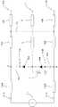
図5はサンプラーの構成例を示す回路図である。図5に示すサンプラーは、高周波信号が入力される入力部1と、高周波信号の信号源のグランド側に接続される入力部2Aおよび入力部2Bと、入力部1に接続される伝送パターン3と、入力部2Aおよび入力部2Bにそれぞれ接続され、伝送パターン3と平行に設けられた伝送パターン4Aおよび伝送パターン4Bと、伝送パターン3に直列に接続された伝送パターン5と、伝送パターン4Aおよび伝送パターン4Bに、それぞれ直列に接続された伝送パターン6Aおよび伝送パターン6Bと、入力された高周波信号を終端する終端抵抗7と、スイッチングにより高周波信号をサンプリングするスイッチダイオード8Aおよびスイッチダイオード8Bと、充電により高周波信号をホールドするホールドコンデンサ9Aおよびホールドコンデンサ9Bと、ストローブ信号となるステップ信号を発生させる信号源11と、信号源11からのストローブ信号が入力されるストローブ入力部11aおよびストローブ入力部11bと、ストローブ入力部11aおよびストローブ入力部11bにそれぞれ接続された伝送パターン12Aおよび伝送パターン12Bと、を備える。 FIG. 5 is a circuit diagram showing a configuration example of the sampler. The sampler shown in FIG. 5 includes an
伝送パターン3、伝送パターン4Aおよび伝送パターン4Bは1組のコプレーナー線路を、伝送パターン5、伝送パターン6Aおよび伝送パターン6Bは1組のコプレーナー線路を、それぞれ構成する。また、伝送パターン6Aおよび伝送パターン6Bは1組のスロット線路を、伝送パターン12Aおよび伝送パターン12Bは1組のスロット線路を、それぞれ構成する。なお、信号源11から見た場合、伝送パターン6Aおよび伝送パターン6Bはスロット線路とみなされ、伝送パターン5は無視される。
次に、この回路の動作について説明する。高周波信号の信号源のグランド側を入力部2Aおよび入力部2Bに接続した状態で、高周波信号を入力部1に入力する。通常時には、端子10Aおよび端子10Bを介して逆バイアスを与えることで、スイッチダイオード8Aおよびスイッチダイオード8Bをオフさせておく。高周波信号の電圧は、伝送パターン3、4A、4Bによるコプレーナー線路、伝送パターン5、6A、6Bによるコプレーナー線路、ホールドコンデンサ9Aおよびホールドコンデンサ9Bを介して、スイッチダイオード8Aおよびスイッチダイオード8Bに印加された状態となる。 Next, the operation of this circuit will be described. A high frequency signal is input to the
サンプリング動作時には、ストローブ入力部11aおよびストローブ入力部11bを介して、信号源11からストローブ信号が与えられる。このストローブ信号は、スロット線路を構成する伝送パターン12Aおよび伝送パターン12Bを伝播する。このとき、伝送パターン12Aおよび伝送パターン12Bに誘起される電圧は、互いに逆の極性を持ったステップパルスを生み出す。このステップパルスは、スイッチダイオード8Aおよびスイッチダイオード8Bの位置を通過してスロット線路を構成する伝送パターン6Aおよび伝送パターン6Bを伝播し、短絡経路14で短絡される。 During the sampling operation, a strobe signal is given from the
短絡経路14における短絡時の反射により、次に、伝送パターン12Aおよび伝送パターン12Bの短絡経路14側(図5において右側)の端部を起点とする、逆極性のステップパルスが、逆方向(図5において左方向)に伝播する。このステップパルスは再びスイッチダイオード8Aおよびスイッチダイオード8Bの位置を逆方向(図5において左方向)に通過する。 Due to the reflection at the time of the short circuit in the
このように、短時間の間に往復する2つのステップパルスが重ね合わされ、図5のP点およびQ点で観測される波形は、幅の細いパルスとなる。パルスの幅はステップパルスの立ち上がり時間と、伝送パターン6Aおよび伝送パターン6Bで形成される伝送路の長さに制限される。ステップパルスの立ち上がりが充分速く、伝送路の長さが適切に設計されていれば、P点およびQ点の波形はインパルス信号となる。このインパルス信号はP点とQ点で逆の極性を持ち、それぞれホールドコンデンサ9Aおよびホールドコンデンサ9Bを介してスイッチダイオード8Aおよびスイッチダイオード8Bをインパルス信号の時間幅だけオンさせる。スイッチダイオード8Aおよびスイッチダイオード8Bがオンしている間、高周波信号はホールドコンデンサ9Aおよびホールドコンデンサ9Bを充電する。スイッチダイオード8Aおよびスイッチダイオード8Bがオフした後に、端子10Aおよび端子10Bを介して充電電圧を取り出し、これをサンプリング電圧として使用する。
しかし、現実の回路では使用する部品や回路の実装状況に応じて、寄生容量、寄生インダクタンス、接点に起因する損失等が発生する。 However, in an actual circuit, a parasitic capacitance, a parasitic inductance, a loss due to a contact, and the like are generated depending on a component to be used and a mounting state of the circuit.
図6は現実の実装回路における等価回路を示す回路図である。図6に示す伝送パターン21〜23は1組のコプレーナー線路を構成する。理想的には高周波信号はスイッチダイオード8Aおよびスイッチダイオード8Bの直近で終端されることが望ましい。しかし、各部品の大きさの制約により、実際には伝送パターン21〜23に相当する不要な線路が形成されてしまう。 FIG. 6 is a circuit diagram showing an equivalent circuit in an actual mounting circuit.
また、スイッチダイオード8Aおよびスイッチダイオード8Bには、それぞれコンデンサ24Aおよびコンデンサ24Bとして示す寄生容量が存在する。さらに、終端抵抗7には、コンデンサ25として示す寄生容量が存在する。 Further, the
図6のインダクタンス26はステップパルスを短絡させる経路の寄生インダクタンスを代表している。コンデンサ27Aおよびコンデンサ27Bは、伝送パターン3、伝送パターン4A、伝送パターン4B、伝送パターン5、伝送パターン6A、伝送パターン6B、あるいは短絡経路14相互間の容量結合に基づく寄生容量を代表している。また、抵抗28は、伝送パターン3、伝送パターン4A、伝送パターン4B、伝送パターン5、伝送パターン6A、伝送パターン6Bや、入力部1、入力部2Aあるいは入力部2Bへの接続のためのコネクタなどに存在する損失を代表している。 The
これらの寄生容量、寄生インダクタンス、損失等は、実際には伝送線路やその接続部分などに分布定数的に存在するものであるが、図6では回路中に挿入された各素子に代表して表現している。 These parasitic capacitances, parasitic inductances, losses, and the like actually exist in a distributed constant manner in the transmission line and its connection part, but in FIG. 6, they are represented as representative elements inserted in the circuit. is doing.
図6に示すような寄生容量、寄生インダクタンス、損失等は、サンプラーの性能を制限する要因となる。 Parasitic capacitance, parasitic inductance, loss, and the like as shown in FIG. 6 are factors that limit the performance of the sampler.
例えば、スイッチダイオード8Aおよびスイッチダイオード8Bの寄生容量はサンプラーの動作周波数を制限する。また、抵抗28により代表される損失は実際には周波数特性を持ち、周波数が高いほど損失が大きくなるため、これも動作周波数の制限となる。 For example, the parasitic capacitances of the
また、インダクタンス26に代表されるステップパルスを短絡させる経路の寄生インダクタンスもまた、サンプラーの動作周波数を制限する。さらに、コンデンサ27Aおよびコンデンサ27Bが代表する寄生容量は、伝送パターン3、伝送パターン4A、伝送パターン4B、伝送パターン5、伝送パターン6A、伝送パターン6Bによる伝送線路のインピーダンスを乱す。その結果、インピーダンスの不整合による反射を生じ、高周波信号が正常に伝送されなくなり、動作周波数が制限される。 Further, the parasitic inductance of the path for short-circuiting the step pulse represented by the
さらに、従来のサンプラーにおいては、ストローブ信号の振幅不足によるダイナミックレンジの制限が発生しやすいという問題がある。ストローブ信号には、スイッチダイオード8Aおよびスイッチダイオード8Bをオンさせるのに必要なだけの振幅が要求される。スイッチダイオード8Aおよびスイッチダイオード8Bは逆バイアスされており、さらに高周波信号が印加されて逆バイアスが深くなった状態からスイッチダイオード8Aおよびスイッチダイオード8Bをオンさせなければならない。このため、ストローブ信号には大きな振幅が必要となり、その振幅の大きさがサンプラーのダイナミックレンジに影響する。 Further, the conventional sampler has a problem that the dynamic range is likely to be limited due to insufficient amplitude of the strobe signal. The strobe signal is required to have an amplitude sufficient to turn on the
一方、ストローブ信号の立ち上がり時間は動作速度に影響するため、動作周波数の広いサンプラーを得るためには、その立ち上がりが速いほどよい。 On the other hand, since the rise time of the strobe signal affects the operation speed, it is better that the rise time is faster in order to obtain a sampler with a wide operation frequency.
このように、立ち上がりが速く振幅が大きいストローブ信号が必要であるが、立ち上がりの速い信号は伝送が困難であり損失も大きくなるため、その両立は困難である。 As described above, a strobe signal having a fast rise and a large amplitude is required. However, since a signal having a fast rise is difficult to transmit and has a large loss, it is difficult to achieve both.
本発明の目的は、広帯域なサンプラー、あるいはダイナミックレンジの大きいサンプラーを提供することにある。 An object of the present invention is to provide a broadband sampler or a sampler with a large dynamic range.
本発明のサンプラーは、インパルス信号によりスイッチング素子をスイッチさせて高周波信号をサンプリングするサンプラーにおいて、高周波信号が前記スイッチング素子に流れ込む経路中に存在する寄生容量を補償する補償回路を設けたことを特徴とする。
このサンプラーによれば、補償回路が寄生容量を補償するので、サンプラーの動作帯域を拡大できる。The sampler of the present invention is a sampler that samples a high-frequency signal by switching a switching element with an impulse signal, and is provided with a compensation circuit that compensates for parasitic capacitance existing in a path through which the high-frequency signal flows into the switching element. To do.
According to this sampler, since the compensation circuit compensates for the parasitic capacitance, the operating band of the sampler can be expanded.
前記寄生容量は前記スイッチング素子の寄生容量であってもよい。 The parasitic capacitance may be a parasitic capacitance of the switching element.
本発明のサンプラーは、インパルス信号によりスイッチング素子をスイッチさせて高周波信号をサンプリングするサンプラーにおいて、高周波信号が前記スイッチング素子に流れ込む経路中に存在する損失を補償する補償回路を設けたことを特徴とする。
このサンプラーによれば、補償回路が損失を補償するので、サンプラーの動作帯域を拡大できる。The sampler of the present invention is characterized in that, in a sampler that switches a switching element by an impulse signal and samples a high-frequency signal, a compensation circuit that compensates for a loss existing in a path through which the high-frequency signal flows into the switching element is provided. .
According to this sampler, since the compensation circuit compensates for the loss, the operating band of the sampler can be expanded.
本発明のサンプラーは、インパルス信号によりスイッチング素子をスイッチさせて高周波信号をサンプリングするサンプラーにおいて、高周波信号が前記スイッチング素子に流れ込む経路中に、前記経路のインピーダンス整合のためのインダクタンスを直列に挿入したことを特徴とする。
このサンプラーによれば、インダクタンスにより経路のインピーダンス整合が行われるので、サンプラーの動作帯域を拡大できる。In the sampler of the present invention, in a sampler that switches a switching element with an impulse signal and samples a high frequency signal, an inductance for impedance matching of the path is inserted in series in a path through which the high frequency signal flows into the switching element. It is characterized by.
According to this sampler, impedance matching of the path is performed by the inductance, so that the operating band of the sampler can be expanded.
本発明のサンプラーは、インパルス信号によりスイッチング素子をスイッチさせて高周波信号をサンプリングするサンプラーにおいて、高周波信号が前記スイッチング素子に流れ込む経路中にハイパス特性を有する補償回路を設けたことを特徴とする。
このサンプラーによれば、ハイパス特性を有する補償回路により経路の周波数特性が補償されるので、サンプラーの動作帯域を拡大できる。The sampler of the present invention is characterized in that in a sampler that samples a high frequency signal by switching a switching element by an impulse signal, a compensation circuit having a high-pass characteristic is provided in a path through which the high frequency signal flows into the switching element.
According to this sampler, the frequency characteristic of the path is compensated by the compensation circuit having a high-pass characteristic, so that the operating band of the sampler can be expanded.
本発明のサンプラーは、元信号と、元信号が反射されて形成された反射信号とが合成されて形成されたインパルス信号によりスイッチング素子をスイッチさせて高周波信号をサンプリングするサンプラーにおいて、前記元信号の反射により前記反射信号を作り出す短絡経路の近傍に、短絡経路に基づく容量成分を補償する高インピーダンスの線路を挿入したことを特徴とする。
このサンプラーによれば、高インピーダンスの線路により短絡経路に基づく容量成分を補償するので、高周波信号がスイッチング素子に流れ込む経路の周波数特性が向上してサンプラーの動作帯域を拡大できる。The sampler of the present invention is a sampler that samples a high-frequency signal by switching a switching element with an impulse signal formed by combining an original signal and a reflected signal formed by reflecting the original signal. A high-impedance line that compensates for a capacitance component based on the short-circuit path is inserted in the vicinity of the short-circuit path that generates the reflected signal by reflection.
According to this sampler, since the capacitive component based on the short-circuit path is compensated by the high impedance line, the frequency characteristic of the path through which the high-frequency signal flows into the switching element is improved, and the operating band of the sampler can be expanded.
本発明のサンプラーは、元信号と、元信号が反射されて形成された反射信号とが合成されて形成されたインパルス信号によりスイッチング素子をスイッチさせて高周波信号をサンプリングするサンプラーにおいて、前記元信号の反射により前記反射信号を作り出す短絡経路を、基板上の導体パターン間を短絡する金属ブロックを用いて形成したことを特徴とする。
このサンプラーによれば、短絡経路を、金属ブロックを用いて形成したので、低インピーダンスの短絡経路を得ることができ、短絡経路の周波数特性が向上してサンプラーの動作帯域を拡大できる。The sampler of the present invention is a sampler that samples a high-frequency signal by switching a switching element with an impulse signal formed by combining an original signal and a reflected signal formed by reflecting the original signal. A short-circuit path that generates the reflected signal by reflection is formed using a metal block that short-circuits between conductor patterns on the substrate.
According to this sampler, since the short-circuit path is formed using the metal block, a low-impedance short-circuit path can be obtained, the frequency characteristics of the short-circuit path can be improved, and the operating band of the sampler can be expanded.
本発明のサンプラーは、元信号と、元信号が反射されて形成された反射信号とが合成されて形成されたインパルス信号によりスイッチング素子をスイッチさせて高周波信号をサンプリングするサンプラーにおいて、前記元信号の経路のインピーダンスを高くする線路ないし回路を設けたことを特徴とする。
このサンプラーによれば、元信号の経路のインピーダンスを高くする線路ないし回路を設けたので、元信号および反射信号の振幅を拡大でき、インパルス信号の振幅も増大するため、サンプラーのダイナミックレンジを拡大できる。The sampler of the present invention is a sampler that samples a high-frequency signal by switching a switching element with an impulse signal formed by combining an original signal and a reflected signal formed by reflecting the original signal. A line or circuit for increasing the impedance of the path is provided.
According to this sampler, since the line or circuit for increasing the impedance of the path of the original signal is provided, the amplitude of the original signal and the reflected signal can be expanded, and the amplitude of the impulse signal is also increased, so that the dynamic range of the sampler can be expanded. .
本発明のサンプラーによれば、補償回路が寄生容量を補償するので、サンプラーの動作帯域を拡大できる。 According to the sampler of the present invention, since the compensation circuit compensates for the parasitic capacitance, the operating band of the sampler can be expanded.
本発明のサンプラーによれば、補償回路が損失を補償するので、サンプラーの動作帯域を拡大できる。 According to the sampler of the present invention, since the compensation circuit compensates for the loss, the operating band of the sampler can be expanded.
本発明のサンプラーによれば、インダクタンスにより経路のインピーダンス整合が行われるので、サンプラーの動作帯域を拡大できる。 According to the sampler of the present invention, the impedance matching of the path is performed by the inductance, so that the operating band of the sampler can be expanded.
本発明のサンプラーによれば、ハイパス特性を有する補償回路により経路の周波数特性が補償されるので、サンプラーの動作帯域を拡大できる。 According to the sampler of the present invention, the frequency characteristic of the path is compensated by the compensation circuit having a high-pass characteristic, so that the operating band of the sampler can be expanded.
本発明のサンプラーによれば、高インピーダンスの線路により短絡経路に基づく容量成分を補償するので、高周波信号がスイッチング素子に流れ込む経路の周波数特性が向上してサンプラーの動作帯域を拡大できる。 According to the sampler of the present invention, the capacitance component based on the short-circuit path is compensated by the high impedance line, so that the frequency characteristic of the path through which the high-frequency signal flows into the switching element is improved, and the operating band of the sampler can be expanded.
本発明のサンプラーによれば、短絡経路を、金属ブロックを用いて形成したので、低インピーダンスの短絡経路を得ることができ、短絡経路の周波数特性が向上してサンプラーの動作帯域を拡大できる。 According to the sampler of the present invention, since the short-circuit path is formed using the metal block, a low-impedance short-circuit path can be obtained, and the frequency characteristic of the short-circuit path can be improved and the operating band of the sampler can be expanded.
本発明のサンプラーによれば、元信号の経路のインピーダンスを高くする線路ないし回路を設けたので、元信号および反射信号の振幅を拡大でき、インパルス信号の振幅も増大するため、サンプラーのダイナミックレンジを拡大できる。 According to the sampler of the present invention, since the line or circuit for increasing the impedance of the path of the original signal is provided, the amplitude of the original signal and the reflected signal can be expanded, and the amplitude of the impulse signal is also increased. Can be expanded.
以下、図1〜図4を参照して、本発明によるサンプラーの実施形態について説明する。 Hereinafter, an embodiment of a sampler according to the present invention will be described with reference to FIGS.
図1は本実施形態のサンプラーの構成を示す等価回路図である。 FIG. 1 is an equivalent circuit diagram showing the configuration of the sampler of this embodiment.
本実施形態のサンプラーは、高周波信号が入力される入力部1と、高周波信号の信号源のグランド側に接続される入力部2Aおよび入力部2Bと、入力部1に接続される伝送パターン3と、入力部2Aおよび入力部2Bにそれぞれ接続され、伝送パターン3と平行に設けられた伝送パターン4Aおよび伝送パターン4Bと、伝送パターン3に直列に接続された伝送パターン5と、伝送パターン4Aおよび伝送パターン4Bに、それぞれ直列に接続された伝送パターン6Aおよび伝送パターン6Bと、入力された高周波信号を終端する終端抵抗7と、スイッチングにより高周波信号をサンプリングするスイッチダイオード8Aおよびスイッチダイオード8Bと、充電により高周波信号をホールドするホールドコンデンサ9Aおよびホールドコンデンサ9Bと、ストローブ信号となるステップ信号を発生させる信号源11と、信号源11からのストローブ信号が入力されるストローブ入力部11aおよびストローブ入力部11bと、ストローブ入力部11aおよびストローブ入力部11bにそれぞれ接続されたテーパ線路34Aおよびテーバ線路34Bと、を備える。 The sampler of the present embodiment includes an
伝送パターン3、伝送パターン4Aおよび伝送パターン4Bは1組のコプレーナー線路を、伝送パターン5、伝送パターン6Aおよび伝送パターン6Bは1組のコプレーナー線路を、それぞれ構成する。また、伝送パターン6Aおよび伝送パターン6Bは1組のスロット線路を、テーパ線路34Aおよびテーパ線路34Bは1組のスロット線路を、それぞれ構成する。なお、信号源11から見た場合、伝送パターン6Aおよび伝送パターン6Bはスロット線路とみなされ、伝送パターン5は無視される。
図1に示す伝送パターン21〜23は1組のコプレーナー線路を構成する。伝送パターン21〜23は、各部品の大きさの制約等により形成される線路の電気特性を等価的に示している。 The
また、スイッチダイオード8Aおよびスイッチダイオード8Bには、それぞれコンデンサ24Aおよびコンデンサ24Bとして示す寄生容量が存在する。さらに、終端抵抗7には、コンデンサ25として示す寄生容量が存在する。 Further, the
図1のインダクタンス26はステップパルスを短絡させる経路の寄生インダクタンスを代表している。コンデンサ27Aおよびコンデンサ27Bは、伝送パターン3、伝送パターン4A、伝送パターン4B、伝送パターン5、伝送パターン6A、伝送パターン6B、あるいは短絡経路14相互間の容量結合に基づく寄生容量を代表している。また、抵抗28は、伝送パターン3、伝送パターン4A、伝送パターン4B、伝送パターン5、伝送パターン6A、伝送パターン6Bや、入力部1、入力部2Aあるいは入力部2Bへの接続のためのコネクタなどに存在する損失を代表している。 The
これらの寄生容量、寄生インダクタンス、損失等は、実際には伝送線路やその接続部分などに分布定数的に存在するものであるが、図1では回路中に挿入された各素子に代表して表現している。 These parasitic capacitances, parasitic inductances, losses, and the like actually exist in a distributed constant manner in the transmission line and the connection portion thereof, but in FIG. 1, they are represented by representative elements inserted in the circuit. is doing.
図1に示すように、本実施形態のサンプラーでは、インダクタンス31およびインダクタンス32をスイッチダイオード8Aおよびスイッチダイオード8Bの近傍に挿入している。このインダクタンス31およびインダクタンス32は、コンデンサ24Aおよびコンデンサ24Bとして示すスイッチダイオード8Aおよびスイッチダイオード8Bの寄生容量を補償し、回路のインピーダンスを伝送パターン3、伝送パターン4A、伝送パターン4B、伝送パターン5、伝送パターン6A、伝送パターン6Bによる伝送線路と整合させる機能を持つ。実際にはインダクタンス31およびインダクタンス32の値は小さくてよいため、インピーダンスが高めの伝送線路を該当する位置に挿入している。 As shown in FIG. 1, in the sampler of this embodiment, an
同様に、終端抵抗7の近傍に挿入されたインダクタンス33は、コンデンサ25として示す終端抵抗7の寄生容量の影響を打ち消している。 Similarly, the
図1に示すように、コンデンサ35aおよび抵抗35bからなるハイパスフィルタ35が、伝送パターン5と直列に挿入されている。このハイパスフィルタ35は、伝送パターン3、伝送パターン4A、伝送パターン4B、伝送パターン5、伝送パターン6A、伝送パターン6B、伝送パターン21〜23からなる伝送線路における損失、および、入力部1、入力部2A、入力部2Bに接続されるコネクタおよびその接点における損失を補償する。これらの損失の周波数特性の逆に近い特性を持つハイパスフィルタ35等を高周波信号の入力経路に挿入することにより、サンプラーの周波数特性を平坦にすることができる。 As shown in FIG. 1, a high-
本実施形態のサンプラーでは、ストローブ信号の振幅を稼ぐために、信号源11から出力されるステップ信号を高インピーダンスで受けるようにしている。図1に示すように、ステップ信号はテーパー線路34Aおよびテーパー線路34Bを介して入力される。テーパー線路34Aおよびテーパー線路34Bによりステップ信号の反射が抑制されるように、インピーダンス変換している。また、伝送パターン22および伝送パターン23で構成されるスロット線路と、伝送パターン6Aおよび伝送パターン6Bで構成されるスロット線路のインピーダンスを、テーパー線路34Aおよびテーパー線路34Bによる変換後のインピーダンスに整合させている。このように、ステップ信号を信号源11よりも高インピーダンスで受けることで、スイッチダイオード8Aおよびスイッチダイオード8Bに与えるストローブ信号の振幅を拡大している。 In the sampler of this embodiment, the step signal output from the
このため、本実施形態のサンプラーでは、立ち上がりが速く、しかも振幅の大きなストローブ信号を得ることができるため、サンプラーのダイナミックレンジを効果的に拡大できる。 For this reason, in the sampler of the present embodiment, a strobe signal that rises quickly and has a large amplitude can be obtained, so that the dynamic range of the sampler can be effectively expanded.
コンデンサ27Aおよびコンデンサ27Bにより代表される、伝送パターン3、伝送パターン4A、伝送パターン4B、伝送パターン5、伝送パターン6A、伝送パターン6B、あるいは短絡経路14相互間の容量結合に基づく寄生容量により、伝送パターン3、伝送パターン4A、伝送パターン4B、伝送パターン5、伝送パターン6A、伝送パターン6Bからなる伝送線路のインピーダンスが乱れ、低めのインピーダンスとなる。本実施形態のサンプラーでは、その寄生容量を打ち消すために短絡経路14の近傍にインピーダンスの高い伝送線路36、伝送線路37A、伝送線路37B、伝送線路38、伝送線路39A、伝送線路39Bを挿入する。これにより、寄生容量の容量成分が打ち消され、インピーダンスの乱れを最小限に抑えることができる。 Transmission by parasitic capacitance based on capacitive coupling between
図2は本実施形態のサンプラーの実装状態を示す図であり、図2(a)は平面図、図2(b)は図2(a)のIIb−IIb線断面図である。 2A and 2B are diagrams illustrating a mounting state of the sampler according to the present embodiment. FIG. 2A is a plan view, and FIG. 2B is a cross-sectional view taken along the line IIb-IIb in FIG.
図2(a)および図2(b)に示すように、本実施形態のサンプラーは、基板51上にスイッチダイオード8Aおよびスイッチダイオード8B、その他の部品が内蔵されてサンプラーの回路を構成するモジュール52が実装され、構成される。 As shown in FIG. 2A and FIG. 2B, the sampler of this embodiment includes a
基板51には、伝送パターン3に相当する導体パターン53と、伝送パターン4Aおよび伝送パターン4Bに相当する導体パターン54および導体パターン55とが形成されている。導体パターン53、導体パターン54および導体パターン55には同軸ケーブル56により伝送される高周波信号が与えられる。導体パターン54および導体パターン55は、高周波信号の信号源のグランド側に接続される。 On the
短絡ブロック60は導体パターン54および導体パターン55を接続するトンネル状の金属製ブロックであり、図1における短絡経路14を構成する。短絡ブロック60は広い面積で導体パターン54および導体パターン55に対し接続されるとともに、短絡経路14としての断面積を大きくできる。また、短絡ブロック60に形成された切り欠き61により、導体パターン53との間の距離を充分に確保できる。このため、インダクタンス26、コンデンサ27Aおよびコンデンサ27B(図1)で示されるインダクタンス成分や寄生容量成分を抑制でき、理想に近い短絡経路14が構成される。このため、基板上での配線やワイヤボンディングにより短絡経路14を構成する場合に比較して、サンプラーの動作周波数を効果的に拡大できる。なお、短絡ブロック60の形状を選択して、最適なインピーダンス特性を持たせることもできる。 The short-
図3は別の実装状態を示す図であり、図3(a)は平面図、図3(b)は図3(a)のIIIb−IIIb線方向から見た側面図、図3(c)は図3(a)のIIIc−IIIc線断面図である。 FIG. 3 is a view showing another mounting state, FIG. 3 (a) is a plan view, FIG. 3 (b) is a side view seen from the direction of line IIIb-IIIb in FIG. 3 (a), and FIG. 3 (c). These are the IIIc-IIIc sectional view taken on the line of Fig.3 (a).
図3に示す例では、短絡ブロック60(図2)に代えて、基板を覆う金属製のパッケージを用いて、短絡経路を構成している。 In the example shown in FIG. 3, instead of the short circuit block 60 (FIG. 2), a short circuit path is configured using a metal package that covers the substrate.
図3(a)〜(c)に示すように、基板51A上には、スイッチダイオード8Aおよびスイッチダイオード8B、その他の部品が内蔵されてサンプラーの回路を構成するモジュール52が実装される。 As shown in FIGS. 3A to 3C, on the
基板51Aには、伝送パターン3に相当する導体パターン53Aと、伝送パターン4Aおよび伝送パターン4Bに相当する導体パターン54Aおよび導体パターン55Aとが形成されている。導体パターン53A、導体パターン54Aおよび導体パターン55Aには同軸ケーブル56Aにより伝送される高周波信号が与えられる。導体パターン54Aおよび導体パターン55Aは、高周波信号の信号源のグランド側に接続される。 A
基板51A上のモジュール52をその内部空間72に収容するパッケージ70は、同軸ケーブル56Aが挿入される切り欠き71が形成された金属製のブロックとして構成されるとともに、図1における短絡経路14を構成する。図3(a)〜(c)に示すように、パッケージ70はその端面において広い面積で導体パターン54Aおよび導体パターン55Aに対し接続されるとともに、短絡経路14としての断面積を大きくできる。また、パッケージ70に形成された切り欠き71により、導体パターン53Aとの間の距離を充分に確保できる。このため、インダクタンス26、コンデンサ27Aおよびコンデンサ27B(図1)で示されるインダクタンス成分や寄生容量成分を抑制でき、理想に近い短絡経路14が構成される。このため、基板上での配線やワイヤボンディングにより短絡経路14を構成する場合に比較して、サンプラーの動作周波数を効果的に拡大できる。なお、パッケージ70の形状を選択して、最適なインピーダンス特性を持たせることもできる。 A
このように、パッケージ70に近接してモジュール52を実装できる場合には、パッケージ70を利用して短絡経路14を構成することができる。 As described above, when the
図4の構成は、図1の構成におけるハイパスフィルタ35に代えて、同様のハイパス特性を持つテーパー線路41を挿入することで、抵抗28として示す損失を補償する例を示している。図4において伝送パターン42および伝送パターン43は、テーパー線路41との組み合わせでインピーダンス整合を図るためのものである。 The configuration of FIG. 4 shows an example in which the loss shown as the
以上説明したように、本発明のサンプラーによれば、補償回路が寄生容量を補償するので、サンプラーの動作帯域を拡大できる。また、補償回路が損失を補償するので、サンプラーの動作帯域を拡大できる。また、インダクタンスにより経路のインピーダンス整合が行われるので、サンプラーの動作帯域を拡大できる。また、ハイパス特性を有する補償回路により経路の周波数特性が補償されるので、サンプラーの動作帯域を拡大できる。また、高インピーダンスの線路により短絡経路に基づく容量成分を補償するので、短絡経路の周波数特性が向上してサンプラーの動作帯域を拡大できる。また、短絡経路を、金属ブロックを用いて形成したので、低インピーダンスの短絡経路を得ることができ、短絡経路の周波数特性が向上してサンプラーの動作帯域を拡大できる。 As described above, according to the sampler of the present invention, since the compensation circuit compensates for the parasitic capacitance, the operating band of the sampler can be expanded. In addition, since the compensation circuit compensates for the loss, the operating band of the sampler can be expanded. Further, since the impedance matching of the path is performed by the inductance, the operating band of the sampler can be expanded. Further, since the frequency characteristic of the path is compensated by the compensation circuit having a high-pass characteristic, the operating band of the sampler can be expanded. In addition, since the capacitance component based on the short-circuit path is compensated by the high impedance line, the frequency characteristic of the short-circuit path is improved and the operating band of the sampler can be expanded. Further, since the short-circuit path is formed using a metal block, a low-impedance short-circuit path can be obtained, the frequency characteristics of the short-circuit path can be improved, and the operating band of the sampler can be expanded.
さらに、本発明のサンプラーによれば、元信号の経路のインピーダンスを高くする線路ないし回路を設けたので、元信号および反射信号の振幅を拡大でき、インパルス信号の振幅も増大するため、サンプラーのダイナミックレンジを拡大できる。 Furthermore, according to the sampler of the present invention, since the line or circuit for increasing the impedance of the path of the original signal is provided, the amplitude of the original signal and the reflected signal can be enlarged and the amplitude of the impulse signal is also increased. The range can be expanded.
本発明の適用範囲は上記実施形態に限定されることはない。本発明は測定装置に限定されず、例えば、ミキサーにも適用される。本発明は、インパルス信号によりスイッチング素子をスイッチさせて高周波信号をサンプリングするサンプラーに対し、広く適用することができる。 The scope of application of the present invention is not limited to the above embodiment. The present invention is not limited to a measuring apparatus, and is applied to, for example, a mixer. The present invention can be widely applied to a sampler that switches a switching element with an impulse signal and samples a high-frequency signal.
31 インダクタンス
32 インダクタンス
33 インダクタンス
34A,34B テーパー線路
35 ハイパスフィルタ
36,37A,37B,38,39A,39B 伝送線路
31
Claims (8)
Translated fromJapanese高周波信号が前記スイッチング素子に流れ込む経路中に存在する寄生容量を補償する補償回路を設けたことを特徴とするサンプラー。In a sampler that samples a high-frequency signal by switching a switching element with an impulse signal,
A sampler comprising a compensation circuit for compensating for parasitic capacitance existing in a path through which a high-frequency signal flows into the switching element.
高周波信号が前記スイッチング素子に流れ込む経路中に存在する損失を補償する補償回路を設けたことを特徴とするサンプラー。In a sampler that samples a high-frequency signal by switching a switching element with an impulse signal,
A sampler comprising a compensation circuit for compensating for a loss present in a path through which a high-frequency signal flows into the switching element.
高周波信号が前記スイッチング素子に流れ込む経路中に、前記経路のインピーダンス整合のためのインダクタンスを直列に挿入したことを特徴とするサンプラー。In a sampler that samples a high-frequency signal by switching a switching element with an impulse signal,
A sampler, wherein an inductance for impedance matching of the path is inserted in series in a path through which a high-frequency signal flows into the switching element.
高周波信号が前記スイッチング素子に流れ込む経路中にハイパス特性を有する補償回路を設けたことを特徴とするサンプラー。In a sampler that samples a high-frequency signal by switching a switching element with an impulse signal,
A sampler comprising a compensation circuit having a high-pass characteristic in a path through which a high-frequency signal flows into the switching element.
前記元信号の反射により前記反射信号を作り出す短絡経路の近傍に、短絡経路に基づく容量成分を補償する高インピーダンスの線路を挿入したことを特徴とするサンプラー。In a sampler that samples a high-frequency signal by switching a switching element with an impulse signal formed by combining an original signal and a reflection signal formed by reflecting the original signal,
A sampler, wherein a high-impedance line that compensates for a capacitance component based on a short circuit path is inserted in the vicinity of a short circuit path that generates the reflected signal by reflecting the original signal.
前記元信号の反射により前記反射信号を作り出す短絡経路を、基板上の導体パターン間を短絡する金属ブロックを用いて形成したことを特徴とするサンプラー。In a sampler that samples a high-frequency signal by switching a switching element with an impulse signal formed by combining an original signal and a reflection signal formed by reflecting the original signal,
A sampler, wherein a short-circuit path for generating the reflected signal by reflecting the original signal is formed using a metal block that short-circuits between conductor patterns on a substrate.
前記元信号の経路のインピーダンスを高くする線路ないし回路を設けたことを特徴とするサンプラー。
In a sampler that samples a high-frequency signal by switching a switching element with an impulse signal formed by combining an original signal and a reflection signal formed by reflecting the original signal,
A sampler comprising a line or a circuit for increasing the impedance of the original signal path.
Priority Applications (1)
| Application Number | Priority Date | Filing Date | Title |
|---|---|---|---|
| JP2005309166AJP4877572B2 (en) | 2005-10-25 | 2005-10-25 | sampler |
Applications Claiming Priority (1)
| Application Number | Priority Date | Filing Date | Title |
|---|---|---|---|
| JP2005309166AJP4877572B2 (en) | 2005-10-25 | 2005-10-25 | sampler |
Publications (2)
| Publication Number | Publication Date |
|---|---|
| JP2007120947Atrue JP2007120947A (en) | 2007-05-17 |
| JP4877572B2 JP4877572B2 (en) | 2012-02-15 |
Family
ID=38144971
Family Applications (1)
| Application Number | Title | Priority Date | Filing Date |
|---|---|---|---|
| JP2005309166AExpired - Fee RelatedJP4877572B2 (en) | 2005-10-25 | 2005-10-25 | sampler |
Country Status (1)
| Country | Link |
|---|---|
| JP (1) | JP4877572B2 (en) |
Citations (7)
| Publication number | Priority date | Publication date | Assignee | Title |
|---|---|---|---|---|
| JPH02212773A (en)* | 1988-12-08 | 1990-08-23 | Hewlett Packard Co <Hp> | Sampler |
| JPH0360533A (en)* | 1989-07-28 | 1991-03-15 | Matsushita Electric Ind Co Ltd | Antenna changeover switch for television high frequency signal |
| JPH09130285A (en)* | 1995-11-06 | 1997-05-16 | Alps Electric Co Ltd | Input circuit for television tuner |
| JPH10308602A (en)* | 1997-05-02 | 1998-11-17 | Fujitsu Ltd | High frequency switch circuit |
| JPH1155002A (en)* | 1997-06-03 | 1999-02-26 | Matsushita Electric Ind Co Ltd | Dual-frequency switch, dual-frequency antenna duplexer, and dual-frequency band mobile communication device using the same |
| JPH11112375A (en)* | 1997-10-08 | 1999-04-23 | Alps Electric Co Ltd | Television signal receiving tuner |
| JPH11205188A (en)* | 1998-01-16 | 1999-07-30 | Mitsubishi Electric Corp | Transmission / reception switching circuit |
- 2005
- 2005-10-25JPJP2005309166Apatent/JP4877572B2/ennot_activeExpired - Fee Related
Patent Citations (7)
| Publication number | Priority date | Publication date | Assignee | Title |
|---|---|---|---|---|
| JPH02212773A (en)* | 1988-12-08 | 1990-08-23 | Hewlett Packard Co <Hp> | Sampler |
| JPH0360533A (en)* | 1989-07-28 | 1991-03-15 | Matsushita Electric Ind Co Ltd | Antenna changeover switch for television high frequency signal |
| JPH09130285A (en)* | 1995-11-06 | 1997-05-16 | Alps Electric Co Ltd | Input circuit for television tuner |
| JPH10308602A (en)* | 1997-05-02 | 1998-11-17 | Fujitsu Ltd | High frequency switch circuit |
| JPH1155002A (en)* | 1997-06-03 | 1999-02-26 | Matsushita Electric Ind Co Ltd | Dual-frequency switch, dual-frequency antenna duplexer, and dual-frequency band mobile communication device using the same |
| JPH11112375A (en)* | 1997-10-08 | 1999-04-23 | Alps Electric Co Ltd | Television signal receiving tuner |
| JPH11205188A (en)* | 1998-01-16 | 1999-07-30 | Mitsubishi Electric Corp | Transmission / reception switching circuit |
Also Published As
| Publication number | Publication date |
|---|---|
| JP4877572B2 (en) | 2012-02-15 |
Similar Documents
| Publication | Publication Date | Title |
|---|---|---|
| JP3629346B2 (en) | Signal transmission system and transmission line drive circuit | |
| EA200200529A1 (en) | MICROPOSED REJECTABLE FILTERS REJECTABLE BY DIELECTRIC PARAMETRIC DIODE | |
| JPH02212773A (en) | Sampler | |
| US7518385B2 (en) | Probe using high pass ground signal path | |
| JP4809266B2 (en) | Impulse generator using nonlinear transmission line | |
| CN101421931A (en) | Antenna device and electronic equipment using the same | |
| EP2097180B1 (en) | Circuit arrangement for evaluating and/or for activating sound transducers | |
| JPS6384531A (en) | Ultrasonic diagnostic apparatus | |
| JP4877572B2 (en) | sampler | |
| US5212378A (en) | Optical receiver with critical damping resistor | |
| JP2012230176A (en) | Optical module | |
| EP4398600A1 (en) | Ultrasonic transducer and ultrasonic inspection system | |
| US4680498A (en) | Input circuit in ultrasonic apparatus | |
| JP2001257509A (en) | Micro strip line | |
| JP3808845B2 (en) | Ultrasonic diagnostic equipment | |
| JP2003032050A (en) | Preamplifier circuit | |
| US6782055B1 (en) | Receiver circuit for a communication system | |
| JP3715752B2 (en) | Resistance thermometer | |
| JP2800318B2 (en) | Sampling head | |
| JP2800321B2 (en) | Sampling head | |
| JP4062660B2 (en) | Time waveform observation system | |
| CN114384526A (en) | Ultrasonic Sensing Devices and Components | |
| JPH0522056A (en) | Microwave semiconductor circuit and reactance circuit | |
| JP2007295103A (en) | Differential pulse generating apparatus | |
| JP2008051582A (en) | Sampling circuit and testing apparatus |
Legal Events
| Date | Code | Title | Description |
|---|---|---|---|
| A621 | Written request for application examination | Free format text:JAPANESE INTERMEDIATE CODE: A621 Effective date:20080812 | |
| A977 | Report on retrieval | Free format text:JAPANESE INTERMEDIATE CODE: A971007 Effective date:20110304 | |
| A131 | Notification of reasons for refusal | Free format text:JAPANESE INTERMEDIATE CODE: A131 Effective date:20110310 | |
| A521 | Written amendment | Free format text:JAPANESE INTERMEDIATE CODE: A523 Effective date:20110506 | |
| A131 | Notification of reasons for refusal | Free format text:JAPANESE INTERMEDIATE CODE: A131 Effective date:20110825 | |
| A521 | Written amendment | Free format text:JAPANESE INTERMEDIATE CODE: A523 Effective date:20111020 | |
| TRDD | Decision of grant or rejection written | ||
| A01 | Written decision to grant a patent or to grant a registration (utility model) | Free format text:JAPANESE INTERMEDIATE CODE: A01 Effective date:20111104 | |
| A01 | Written decision to grant a patent or to grant a registration (utility model) | Free format text:JAPANESE INTERMEDIATE CODE: A01 | |
| A61 | First payment of annual fees (during grant procedure) | Free format text:JAPANESE INTERMEDIATE CODE: A61 Effective date:20111117 | |
| R150 | Certificate of patent (=grant) or registration of utility model | Free format text:JAPANESE INTERMEDIATE CODE: R150 | |
| FPAY | Renewal fee payment (prs date is renewal date of database) | Free format text:PAYMENT UNTIL: 20141209 Year of fee payment:3 | |
| LAPS | Cancellation because of no payment of annual fees |