JP2007110090A - GaN-based semiconductor light emitting device, light emitting device, image display device, planar light source device, and liquid crystal display device assembly - Google Patents
GaN-based semiconductor light emitting device, light emitting device, image display device, planar light source device, and liquid crystal display device assemblyDownload PDFInfo
- Publication number
- JP2007110090A JP2007110090AJP2006234199AJP2006234199AJP2007110090AJP 2007110090 AJP2007110090 AJP 2007110090AJP 2006234199 AJP2006234199 AJP 2006234199AJP 2006234199 AJP2006234199 AJP 2006234199AJP 2007110090 AJP2007110090 AJP 2007110090A
- Authority
- JP
- Japan
- Prior art keywords
- gan
- layer
- light
- emitting element
- active layer
- Prior art date
- Legal status (The legal status is an assumption and is not a legal conclusion. Google has not performed a legal analysis and makes no representation as to the accuracy of the status listed.)
- Pending
Links
Images


Classifications
- H—ELECTRICITY
- H10—SEMICONDUCTOR DEVICES; ELECTRIC SOLID-STATE DEVICES NOT OTHERWISE PROVIDED FOR
- H10H—INORGANIC LIGHT-EMITTING SEMICONDUCTOR DEVICES HAVING POTENTIAL BARRIERS
- H10H20/00—Individual inorganic light-emitting semiconductor devices having potential barriers, e.g. light-emitting diodes [LED]
- H10H20/80—Constructional details
- H10H20/81—Bodies
- H10H20/822—Materials of the light-emitting regions
- H10H20/824—Materials of the light-emitting regions comprising only Group III-V materials, e.g. GaP
- H10H20/825—Materials of the light-emitting regions comprising only Group III-V materials, e.g. GaP containing nitrogen, e.g. GaN
- B—PERFORMING OPERATIONS; TRANSPORTING
- B82—NANOTECHNOLOGY
- B82Y—SPECIFIC USES OR APPLICATIONS OF NANOSTRUCTURES; MEASUREMENT OR ANALYSIS OF NANOSTRUCTURES; MANUFACTURE OR TREATMENT OF NANOSTRUCTURES
- B82Y20/00—Nanooptics, e.g. quantum optics or photonic crystals
- H—ELECTRICITY
- H04—ELECTRIC COMMUNICATION TECHNIQUE
- H04N—PICTORIAL COMMUNICATION, e.g. TELEVISION
- H04N9/00—Details of colour television systems
- H04N9/12—Picture reproducers
- H04N9/31—Projection devices for colour picture display, e.g. using electronic spatial light modulators [ESLM]
- H04N9/3141—Constructional details thereof
- H04N9/315—Modulator illumination systems
- H—ELECTRICITY
- H10—SEMICONDUCTOR DEVICES; ELECTRIC SOLID-STATE DEVICES NOT OTHERWISE PROVIDED FOR
- H10H—INORGANIC LIGHT-EMITTING SEMICONDUCTOR DEVICES HAVING POTENTIAL BARRIERS
- H10H20/00—Individual inorganic light-emitting semiconductor devices having potential barriers, e.g. light-emitting diodes [LED]
- H10H20/80—Constructional details
- H10H20/81—Bodies
- H10H20/811—Bodies having quantum effect structures or superlattices, e.g. tunnel junctions
- H10H20/812—Bodies having quantum effect structures or superlattices, e.g. tunnel junctions within the light-emitting regions, e.g. having quantum confinement structures
- G—PHYSICS
- G02—OPTICS
- G02F—OPTICAL DEVICES OR ARRANGEMENTS FOR THE CONTROL OF LIGHT BY MODIFICATION OF THE OPTICAL PROPERTIES OF THE MEDIA OF THE ELEMENTS INVOLVED THEREIN; NON-LINEAR OPTICS; FREQUENCY-CHANGING OF LIGHT; OPTICAL LOGIC ELEMENTS; OPTICAL ANALOGUE/DIGITAL CONVERTERS
- G02F1/00—Devices or arrangements for the control of the intensity, colour, phase, polarisation or direction of light arriving from an independent light source, e.g. switching, gating or modulating; Non-linear optics
- G02F1/01—Devices or arrangements for the control of the intensity, colour, phase, polarisation or direction of light arriving from an independent light source, e.g. switching, gating or modulating; Non-linear optics for the control of the intensity, phase, polarisation or colour
- G02F1/13—Devices or arrangements for the control of the intensity, colour, phase, polarisation or direction of light arriving from an independent light source, e.g. switching, gating or modulating; Non-linear optics for the control of the intensity, phase, polarisation or colour based on liquid crystals, e.g. single liquid crystal display cells
- G02F1/133—Constructional arrangements; Operation of liquid crystal cells; Circuit arrangements
- G02F1/1333—Constructional arrangements; Manufacturing methods
- G02F1/1335—Structural association of cells with optical devices, e.g. polarisers or reflectors
- G02F1/1336—Illuminating devices
- G02F1/133602—Direct backlight
- G02F1/133603—Direct backlight with LEDs
- G—PHYSICS
- G02—OPTICS
- G02F—OPTICAL DEVICES OR ARRANGEMENTS FOR THE CONTROL OF LIGHT BY MODIFICATION OF THE OPTICAL PROPERTIES OF THE MEDIA OF THE ELEMENTS INVOLVED THEREIN; NON-LINEAR OPTICS; FREQUENCY-CHANGING OF LIGHT; OPTICAL LOGIC ELEMENTS; OPTICAL ANALOGUE/DIGITAL CONVERTERS
- G02F1/00—Devices or arrangements for the control of the intensity, colour, phase, polarisation or direction of light arriving from an independent light source, e.g. switching, gating or modulating; Non-linear optics
- G02F1/01—Devices or arrangements for the control of the intensity, colour, phase, polarisation or direction of light arriving from an independent light source, e.g. switching, gating or modulating; Non-linear optics for the control of the intensity, phase, polarisation or colour
- G02F1/13—Devices or arrangements for the control of the intensity, colour, phase, polarisation or direction of light arriving from an independent light source, e.g. switching, gating or modulating; Non-linear optics for the control of the intensity, phase, polarisation or colour based on liquid crystals, e.g. single liquid crystal display cells
- G02F1/133—Constructional arrangements; Operation of liquid crystal cells; Circuit arrangements
- G02F1/1333—Constructional arrangements; Manufacturing methods
- G02F1/1335—Structural association of cells with optical devices, e.g. polarisers or reflectors
- G02F1/1336—Illuminating devices
- G02F1/133621—Illuminating devices providing coloured light
- H—ELECTRICITY
- H01—ELECTRIC ELEMENTS
- H01L—SEMICONDUCTOR DEVICES NOT COVERED BY CLASS H10
- H01L2224/00—Indexing scheme for arrangements for connecting or disconnecting semiconductor or solid-state bodies and methods related thereto as covered by H01L24/00
- H01L2224/01—Means for bonding being attached to, or being formed on, the surface to be connected, e.g. chip-to-package, die-attach, "first-level" interconnects; Manufacturing methods related thereto
- H01L2224/02—Bonding areas; Manufacturing methods related thereto
- H01L2224/04—Structure, shape, material or disposition of the bonding areas prior to the connecting process
- H01L2224/06—Structure, shape, material or disposition of the bonding areas prior to the connecting process of a plurality of bonding areas
- H01L2224/0601—Structure
- H01L2224/0603—Bonding areas having different sizes, e.g. different heights or widths
- H—ELECTRICITY
- H01—ELECTRIC ELEMENTS
- H01L—SEMICONDUCTOR DEVICES NOT COVERED BY CLASS H10
- H01L2224/00—Indexing scheme for arrangements for connecting or disconnecting semiconductor or solid-state bodies and methods related thereto as covered by H01L24/00
- H01L2224/01—Means for bonding being attached to, or being formed on, the surface to be connected, e.g. chip-to-package, die-attach, "first-level" interconnects; Manufacturing methods related thereto
- H01L2224/10—Bump connectors; Manufacturing methods related thereto
- H01L2224/15—Structure, shape, material or disposition of the bump connectors after the connecting process
- H01L2224/16—Structure, shape, material or disposition of the bump connectors after the connecting process of an individual bump connector
- H01L2224/161—Disposition
- H01L2224/16135—Disposition the bump connector connecting between different semiconductor or solid-state bodies, i.e. chip-to-chip
- H01L2224/16145—Disposition the bump connector connecting between different semiconductor or solid-state bodies, i.e. chip-to-chip the bodies being stacked
- H—ELECTRICITY
- H01—ELECTRIC ELEMENTS
- H01L—SEMICONDUCTOR DEVICES NOT COVERED BY CLASS H10
- H01L2224/00—Indexing scheme for arrangements for connecting or disconnecting semiconductor or solid-state bodies and methods related thereto as covered by H01L24/00
- H01L2224/01—Means for bonding being attached to, or being formed on, the surface to be connected, e.g. chip-to-package, die-attach, "first-level" interconnects; Manufacturing methods related thereto
- H01L2224/42—Wire connectors; Manufacturing methods related thereto
- H01L2224/44—Structure, shape, material or disposition of the wire connectors prior to the connecting process
- H01L2224/45—Structure, shape, material or disposition of the wire connectors prior to the connecting process of an individual wire connector
- H01L2224/45001—Core members of the connector
- H01L2224/45099—Material
- H01L2224/451—Material with a principal constituent of the material being a metal or a metalloid, e.g. boron (B), silicon (Si), germanium (Ge), arsenic (As), antimony (Sb), tellurium (Te) and polonium (Po), and alloys thereof
- H01L2224/45138—Material with a principal constituent of the material being a metal or a metalloid, e.g. boron (B), silicon (Si), germanium (Ge), arsenic (As), antimony (Sb), tellurium (Te) and polonium (Po), and alloys thereof the principal constituent melting at a temperature of greater than or equal to 950°C and less than 1550°C
- H01L2224/45144—Gold (Au) as principal constituent
- H—ELECTRICITY
- H01—ELECTRIC ELEMENTS
- H01L—SEMICONDUCTOR DEVICES NOT COVERED BY CLASS H10
- H01L2224/00—Indexing scheme for arrangements for connecting or disconnecting semiconductor or solid-state bodies and methods related thereto as covered by H01L24/00
- H01L2224/01—Means for bonding being attached to, or being formed on, the surface to be connected, e.g. chip-to-package, die-attach, "first-level" interconnects; Manufacturing methods related thereto
- H01L2224/42—Wire connectors; Manufacturing methods related thereto
- H01L2224/47—Structure, shape, material or disposition of the wire connectors after the connecting process
- H01L2224/48—Structure, shape, material or disposition of the wire connectors after the connecting process of an individual wire connector
- H01L2224/4805—Shape
- H01L2224/4809—Loop shape
- H01L2224/48091—Arched
- H—ELECTRICITY
- H01—ELECTRIC ELEMENTS
- H01L—SEMICONDUCTOR DEVICES NOT COVERED BY CLASS H10
- H01L2224/00—Indexing scheme for arrangements for connecting or disconnecting semiconductor or solid-state bodies and methods related thereto as covered by H01L24/00
- H01L2224/01—Means for bonding being attached to, or being formed on, the surface to be connected, e.g. chip-to-package, die-attach, "first-level" interconnects; Manufacturing methods related thereto
- H01L2224/42—Wire connectors; Manufacturing methods related thereto
- H01L2224/47—Structure, shape, material or disposition of the wire connectors after the connecting process
- H01L2224/48—Structure, shape, material or disposition of the wire connectors after the connecting process of an individual wire connector
- H01L2224/481—Disposition
- H01L2224/48135—Connecting between different semiconductor or solid-state bodies, i.e. chip-to-chip
- H01L2224/48137—Connecting between different semiconductor or solid-state bodies, i.e. chip-to-chip the bodies being arranged next to each other, e.g. on a common substrate
- H—ELECTRICITY
- H01—ELECTRIC ELEMENTS
- H01L—SEMICONDUCTOR DEVICES NOT COVERED BY CLASS H10
- H01L2224/00—Indexing scheme for arrangements for connecting or disconnecting semiconductor or solid-state bodies and methods related thereto as covered by H01L24/00
- H01L2224/01—Means for bonding being attached to, or being formed on, the surface to be connected, e.g. chip-to-package, die-attach, "first-level" interconnects; Manufacturing methods related thereto
- H01L2224/42—Wire connectors; Manufacturing methods related thereto
- H01L2224/47—Structure, shape, material or disposition of the wire connectors after the connecting process
- H01L2224/48—Structure, shape, material or disposition of the wire connectors after the connecting process of an individual wire connector
- H01L2224/481—Disposition
- H01L2224/48151—Connecting between a semiconductor or solid-state body and an item not being a semiconductor or solid-state body, e.g. chip-to-substrate, chip-to-passive
- H01L2224/48221—Connecting between a semiconductor or solid-state body and an item not being a semiconductor or solid-state body, e.g. chip-to-substrate, chip-to-passive the body and the item being stacked
- H01L2224/48245—Connecting between a semiconductor or solid-state body and an item not being a semiconductor or solid-state body, e.g. chip-to-substrate, chip-to-passive the body and the item being stacked the item being metallic
- H01L2224/48247—Connecting between a semiconductor or solid-state body and an item not being a semiconductor or solid-state body, e.g. chip-to-substrate, chip-to-passive the body and the item being stacked the item being metallic connecting the wire to a bond pad of the item
- H—ELECTRICITY
- H01—ELECTRIC ELEMENTS
- H01L—SEMICONDUCTOR DEVICES NOT COVERED BY CLASS H10
- H01L2924/00—Indexing scheme for arrangements or methods for connecting or disconnecting semiconductor or solid-state bodies as covered by H01L24/00
- H01L2924/10—Details of semiconductor or other solid state devices to be connected
- H01L2924/11—Device type
- H01L2924/13—Discrete devices, e.g. 3 terminal devices
- H01L2924/1304—Transistor
- H01L2924/1306—Field-effect transistor [FET]
- H01L2924/13091—Metal-Oxide-Semiconductor Field-Effect Transistor [MOSFET]
- H—ELECTRICITY
- H01—ELECTRIC ELEMENTS
- H01L—SEMICONDUCTOR DEVICES NOT COVERED BY CLASS H10
- H01L2924/00—Indexing scheme for arrangements or methods for connecting or disconnecting semiconductor or solid-state bodies as covered by H01L24/00
- H01L2924/15—Details of package parts other than the semiconductor or other solid state devices to be connected
- H01L2924/181—Encapsulation
- H—ELECTRICITY
- H01—ELECTRIC ELEMENTS
- H01S—DEVICES USING THE PROCESS OF LIGHT AMPLIFICATION BY STIMULATED EMISSION OF RADIATION [LASER] TO AMPLIFY OR GENERATE LIGHT; DEVICES USING STIMULATED EMISSION OF ELECTROMAGNETIC RADIATION IN WAVE RANGES OTHER THAN OPTICAL
- H01S5/00—Semiconductor lasers
- H01S5/30—Structure or shape of the active region; Materials used for the active region
- H01S5/305—Structure or shape of the active region; Materials used for the active region characterised by the doping materials used in the laser structure
- H01S5/3086—Structure or shape of the active region; Materials used for the active region characterised by the doping materials used in the laser structure doping of the active layer
- H01S5/309—Structure or shape of the active region; Materials used for the active region characterised by the doping materials used in the laser structure doping of the active layer doping of barrier layers that confine charge carriers in the laser structure, e.g. the barriers in a quantum well structure
- H—ELECTRICITY
- H01—ELECTRIC ELEMENTS
- H01S—DEVICES USING THE PROCESS OF LIGHT AMPLIFICATION BY STIMULATED EMISSION OF RADIATION [LASER] TO AMPLIFY OR GENERATE LIGHT; DEVICES USING STIMULATED EMISSION OF ELECTROMAGNETIC RADIATION IN WAVE RANGES OTHER THAN OPTICAL
- H01S5/00—Semiconductor lasers
- H01S5/30—Structure or shape of the active region; Materials used for the active region
- H01S5/34—Structure or shape of the active region; Materials used for the active region comprising quantum well or superlattice structures, e.g. single quantum well [SQW] lasers, multiple quantum well [MQW] lasers or graded index separate confinement heterostructure [GRINSCH] lasers
- H01S5/343—Structure or shape of the active region; Materials used for the active region comprising quantum well or superlattice structures, e.g. single quantum well [SQW] lasers, multiple quantum well [MQW] lasers or graded index separate confinement heterostructure [GRINSCH] lasers in AIIIBV compounds, e.g. AlGaAs-laser, InP-based laser
- H01S5/34333—Structure or shape of the active region; Materials used for the active region comprising quantum well or superlattice structures, e.g. single quantum well [SQW] lasers, multiple quantum well [MQW] lasers or graded index separate confinement heterostructure [GRINSCH] lasers in AIIIBV compounds, e.g. AlGaAs-laser, InP-based laser with a well layer based on Ga(In)N or Ga(In)P, e.g. blue laser
- H—ELECTRICITY
- H10—SEMICONDUCTOR DEVICES; ELECTRIC SOLID-STATE DEVICES NOT OTHERWISE PROVIDED FOR
- H10H—INORGANIC LIGHT-EMITTING SEMICONDUCTOR DEVICES HAVING POTENTIAL BARRIERS
- H10H20/00—Individual inorganic light-emitting semiconductor devices having potential barriers, e.g. light-emitting diodes [LED]
- H10H20/80—Constructional details
- H10H20/81—Bodies
- H10H20/819—Bodies characterised by their shape, e.g. curved or truncated substrates
Landscapes
- Engineering & Computer Science (AREA)
- Chemical & Material Sciences (AREA)
- Nanotechnology (AREA)
- Crystallography & Structural Chemistry (AREA)
- Optics & Photonics (AREA)
- Biophysics (AREA)
- Physics & Mathematics (AREA)
- Life Sciences & Earth Sciences (AREA)
- Multimedia (AREA)
- Signal Processing (AREA)
- Led Devices (AREA)
- Led Device Packages (AREA)
- Liquid Crystal (AREA)
Abstract
Translated fromJapaneseDescription
Translated fromJapanese本発明は、GaN系半導体発光素子、並びに、係るGaN系半導体発光素子が組み込まれた発光装置、画像表示装置、面状光源装置、及び、液晶表示装置組立体に関する。 The present invention relates to a GaN-based semiconductor light-emitting element, a light-emitting device incorporating the GaN-based semiconductor light-emitting element, an image display device, a planar light source device, and a liquid crystal display device assembly.
窒化ガリウム(GaN)系化合物半導体から成る活性層を備えた発光素子(GaN系半導体発光素子)においては、活性層の混晶組成や厚さによってバンドギャップエネルギーを制御することにより、紫外から赤外までの広い範囲に亙る発光波長を実現し得る。そして、既に、種々の色を発光するGaN系半導体発光素子が市販されており、画像表示装置や照明装置、検査装置、消毒用光源等、幅広い用途に用いられている。また、青紫色を発光する半導体レーザや発光ダイオード(LED)も開発されており、大容量光ディスクの書込みや読取り用のピックアップとして使用されている。 In a light-emitting device (GaN-based semiconductor light-emitting device) having an active layer made of a gallium nitride (GaN) -based compound semiconductor, the band gap energy is controlled by the mixed crystal composition and thickness of the active layer, so that ultraviolet to infrared is controlled. Emission wavelengths over a wide range up to can be realized. GaN-based semiconductor light-emitting elements that emit various colors are already on the market and are used in a wide range of applications such as image display devices, illumination devices, inspection devices, and disinfection light sources. In addition, semiconductor lasers and light emitting diodes (LEDs) that emit blue-violet light have been developed, and are used as pickups for writing and reading large capacity optical disks.
一般に、GaN系半導体発光素子は、駆動電流(動作電流)が増加すると、発光波長が短波長側にシフトすることが知られており、例えば、駆動電流を20mAから100mAへと増加させた場合、青色の発光領域においては−3nm、緑色の発光領域においては−19nmもの発光波長のシフトが報告されている(例えば、日亜化学工業株式会社製品仕様書NSPB500Sや日亜化学工業株式会社製品仕様書NSPG500S参照)。 In general, it is known that the GaN-based semiconductor light-emitting element shifts the emission wavelength to the short wavelength side when the drive current (operating current) increases. For example, when the drive current is increased from 20 mA to 100 mA, A shift in emission wavelength of −3 nm in the blue light emitting region and −19 nm in the green light emitting region has been reported (for example, Nichia Chemical Co., Ltd. product specification NSPB500S and Nichia Chemical Co., Ltd. product specification). NSPG500S).
そして、このような駆動電流(動作電流)の増加に起因した発光波長のシフトといった現象は、特に、可視光以上の発光波長を有するIn原子を含有するGaN系化合物半導体から成る活性層に共通する問題であり、活性層を構成する井戸層内でのIn原子によるキャリアの局在(例えば、Y. Kawakami, et al., J. Phys. Condens. Matter 13 (2001) pp. 6993 参照)や、格子不整合に起因する内部電界効果(S. F. Chichibu, Materials Science and Engineering B59 (1999) pp.298 参照)が関与していると考えられている。 A phenomenon such as a shift in emission wavelength due to an increase in driving current (operating current) is particularly common in an active layer made of a GaN-based compound semiconductor containing In atoms having an emission wavelength longer than visible light. It is a problem, the localization of carriers by In atoms in the well layer constituting the active layer (for example, see Y. Kawakami, et al., J. Phys. Condens. Matter 13 (2001) pp. 6993), It is thought that the internal electric field effect due to lattice mismatch (see SF Chichibu, Materials Science and Engineering B59 (1999) pp.298) is involved.
そして、このようなGaN系半導体発光素子の発光波長を制御する試みもなされており、例えば、特開2002−237619には、電流値を変化させることによって発光波長が変化する発光ダイオードに、複数のピーク電流値を有するパルス電流を供給することで複数の色を発光させる、発光ダイオードの発光色制御方法が開示されている。これにより、この発光ダイオードの発光色制御方法においては、発光源を1箇所として小型化を図ることができると共に、容易に発光色を制御することができるとされている。 An attempt has been made to control the emission wavelength of such a GaN-based semiconductor light-emitting element. For example, Japanese Patent Application Laid-Open No. 2002-237619 discloses a plurality of light-emitting diodes whose emission wavelength changes by changing the current value. A light emission color control method for a light emitting diode is disclosed, which emits a plurality of colors by supplying a pulse current having a peak current value. As a result, in the light emission color control method of the light emitting diode, it is possible to reduce the size of the light emission source as one place and to easily control the light emission color.
また、例えば、特開2003−22052には、同時に駆動される複数の発光素子を駆動する発光素子の駆動回路が開示されている。この発光素子の駆動回路は、複数の発光素子間の発光波長のばらつきを当該発光素子に供給する電流を制御することによって補正する発光波長補正手段と、複数の発光素子間の輝度のばらつきを補正する発光輝度補正手段とを備えている。これにより、この発光素子の駆動回路においては、製造上のばらつきから均一な発光が困難である発光素子であっても、発光素子間のばらつきを有効に補正することができるとされている。 Also, for example, Japanese Patent Application Laid-Open No. 2003-22052 discloses a light emitting element driving circuit that drives a plurality of light emitting elements that are driven simultaneously. The driving circuit of the light emitting element corrects the variation in light emission wavelength among the plurality of light emitting elements by correcting the emission wavelength correction means for correcting the variation in the light emission wavelength by controlling the current supplied to the light emitting element. And a light emission luminance correction means. Thereby, in the drive circuit of this light emitting element, it is said that even if the light emitting element is difficult to emit uniformly due to manufacturing variations, the variation between the light emitting elements can be effectively corrected.
ところで、GaN系半導体発光素子においては、高効率化のために、井戸層と障壁層とから成る多重量子井戸構造を有する活性層に関して様々な技術が提唱されており、例えば、特表2003−520453には、少なくとも2つの発光活性層、及び、少なくとも1つのバリア層を有する多重量子井戸構造の活性層において、発光活性層あるいはバリア層がチャーピングされた半導体発光素子が開示されている。ここで、チャーピングとは、類似した複数の層の厚さ及び/又は組成が一様とならないように、又は、非対称となるように、これらの層を形成することを意味する。そして、このような構成にすることで、多重量子井戸構造を有するLEDにおける各井戸層の光出力又は光生成効率を高めている。 By the way, in the GaN-based semiconductor light-emitting device, various techniques have been proposed for an active layer having a multiple quantum well structure including a well layer and a barrier layer in order to increase efficiency. For example, JP 2003-520453 A is disclosed. Discloses a semiconductor light emitting device in which a light emitting active layer or a barrier layer is chirped in an active layer having a multiple quantum well structure having at least two light emitting active layers and at least one barrier layer. Here, chirping means forming these layers so that the thickness and / or composition of a plurality of similar layers are not uniform or asymmetric. And by setting it as such a structure, the light output or light generation efficiency of each well layer in LED which has a multiple quantum well structure is raised.
より具体的には、この特許出願公表公報の段落番号[0031]には、第1の例として、LED30における活性層48〜56の厚さのみがチャーピングされており、活性領域36における活性層48,50,52,54及び56は、それぞれ、200,300,400,500及び600オングストロームの厚さを有するように構成されることが開示されている。また、この特許出願公表公報の段落番号[0032]には、第3の例として、バリア層58〜64の厚さのみがチャーピングされており、バリア層は、ほぼ10オングストロームからほぼ500オングストローム以上の間に亙る厚さを有し、n型の下部封層34により近いところに位置するバリア層が、n型の下部封層34から離れたところに位置するバリア層よりも厚くなるように構成されていることが開示されている。 More specifically, in the paragraph number [0031] of this patent application publication, only the thicknesses of the active layers 48 to 56 in the
ところで、GaN系半導体発光素子の光出力を増加させるための一手段として、GaN系半導体発光素子を高い駆動電流(動作電流)にて駆動(動作)させる方法を挙げることができる。しかしながら、このような手段を採用したのでは、上述したとおり、駆動電流(動作電流)の増加に起因した発光波長のシフトといった問題が生じてしまう。従って、従来の動作電流密度に対する発光波長変化の大きなGaN系半導体発光素子においては、輝度を変化させる際、発光色が変化しないように、動作電流密度を一定とし、動作電流のパルス幅(あるいはパルス密度)を変える方式が一般的である。 By the way, as one means for increasing the light output of the GaN-based semiconductor light-emitting element, there can be mentioned a method of driving (operating) the GaN-based semiconductor light-emitting element with a high driving current (operating current). However, when such a means is employed, as described above, there arises a problem of a shift in emission wavelength due to an increase in driving current (operating current). Therefore, in a conventional GaN-based semiconductor light emitting device having a large emission wavelength change with respect to the operating current density, the operating current density is constant so that the emission color does not change when the luminance is changed. A method of changing the density is common.
また、例えば、青色の発光波長を有するGaN系半導体発光素子(発光ダイオード)と、緑色の発光波長を有するGaN系半導体発光素子(発光ダイオード)と、赤色の発光波長を有するAlInGaP系の化合物半導体発光ダイオードとを、各サブピクセルに対応させて配列して構成される画像表示装置において、各発光ダイオードの発光波長のシフトに起因して表示映像にざらつきが生じる場合がある。係る画像表示装置においては、ピクセル(画素)間の色度座標や輝度の調整が行われるものの、上述したように、発光素子の発光波長がシフトし、所望の発光波長とは異なる発光波長となっている場合、調整後の色再現範囲が狭くなってしまうといった問題がある。 Also, for example, a GaN-based semiconductor light-emitting element (light-emitting diode) having a blue emission wavelength, a GaN-based semiconductor light-emitting element (light-emitting diode) having a green emission wavelength, and an AlInGaP-based compound semiconductor light emission having a red emission wavelength In an image display device configured by arranging a diode in correspondence with each sub-pixel, the display image may be rough due to a shift in the emission wavelength of each light-emitting diode. In such an image display device, although chromaticity coordinates and luminance between pixels (pixels) are adjusted, as described above, the emission wavelength of the light-emitting element shifts to become an emission wavelength different from the desired emission wavelength. The color reproduction range after adjustment becomes narrow.
更には、GaN系半導体発光素子と色変換材料とから成る発光装置(例えば、紫外又は青色発光ダイオードと蛍光体粒子とを組み合わせて白色を発光する発光装置)においては、発光装置の輝度(明るさ)を増加させるためにGaN系半導体発光素子の駆動電流(動作電流)を増加させると、色変換材料を励起するGaN系半導体発光素子における発光波長のシフトによって、色変換材料の励起効率が変化してしまい、色度が変化し、色合いが均一な発光装置を得ることが困難な場合がある。 Furthermore, in a light-emitting device composed of a GaN-based semiconductor light-emitting element and a color conversion material (for example, a light-emitting device that emits white light by combining ultraviolet or blue light-emitting diodes and phosphor particles), the luminance (brightness) of the light-emitting device. If the drive current (operating current) of the GaN-based semiconductor light-emitting element is increased to increase the excitation wavelength of the GaN-based semiconductor light-emitting element, the excitation efficiency of the color-converting material changes due to the shift of the emission wavelength in the GaN-based semiconductor light-emitting element that excites the color conversion material. Therefore, there are cases where it is difficult to obtain a light-emitting device in which the chromaticity changes and the hue is uniform.
また、GaN系半導体発光素子を用いたバックライトを備えた液晶表示装置が提案されているが、係る液晶表示装置においても、バックライトの輝度(明るさ)を増加させるためにGaN系半導体発光素子の駆動電流(動作電流)を増加させると、GaN系半導体発光素子における発光波長のシフトによって、色再現範囲が狭くなったり、変化するといった問題が生じる虞がある。 Further, a liquid crystal display device having a backlight using a GaN-based semiconductor light-emitting element has been proposed. In such a liquid crystal display device, a GaN-based semiconductor light-emitting element is used to increase the luminance (brightness) of the backlight. If the driving current (operating current) is increased, the color reproduction range may be narrowed or changed due to the shift of the emission wavelength in the GaN-based semiconductor light emitting device.
GaN系半導体発光素子を用いた照明装置、バックライト、ディスプレイ等のコスト低減や高密度化(高精細化)を実現するには、発光素子の大きさを、従来の300μm角や1mm角といった大きさから更に小さくする必要があるが、同じ動作電流値であれば動作電流密度が高くなることになり、高い動作電流密度での発光波長のシフトが問題となる。また、GaN系半導体発光素子の応用として微小な発光素子を配列した表示装置が挙げられるが、このような微小な発光素子において発光波長のシフトを低減することは表示装置への応用上、重要である。 In order to realize cost reduction and high density (high definition) of lighting devices, backlights, displays, etc. using GaN-based semiconductor light-emitting elements, the size of the light-emitting elements is as large as the conventional 300 μm square or 1 mm square. Although it is necessary to further reduce the operating current density, the operating current density becomes high if the operating current value is the same, and the shift of the emission wavelength at a high operating current density becomes a problem. In addition, as an application of the GaN-based semiconductor light-emitting element, there is a display device in which minute light-emitting elements are arranged. It is important for application to a display device to reduce the shift of the emission wavelength in such a minute light-emitting element. is there.
上述の特許出願公表公報には、バリア層の組成を段階的に変えた計算例が示されているのみで、非対称性とその効果は、具体的には示されていない。更には、上述の特許出願公表公報、あるいは、上述した文献には、動作電流密度の増加によっても発光波長が大きくシフトすることを抑制する技術は、何ら、開示されていない。 The above-mentioned patent application publication only shows a calculation example in which the composition of the barrier layer is changed in stages, and does not specifically show the asymmetry and its effect. Furthermore, the above-mentioned patent application publication or the above-mentioned document does not disclose any technique for suppressing a large shift in the emission wavelength even when the operating current density is increased.
従って、本発明の目的は、動作電流密度の増加に伴う発光波長の大きなシフトを抑制し得る構造を有し、しかも、一層広範囲の輝度制御を行うことを可能とするGaN系半導体発光素子、並びに、係るGaN系半導体発光素子が組み込まれた発光装置、画像表示装置、面状光源装置、及び、液晶表示装置組立体を提供することにある。 Accordingly, an object of the present invention is to provide a GaN-based semiconductor light-emitting device that has a structure capable of suppressing a large shift in emission wavelength accompanying an increase in operating current density, and that can perform a wider range of luminance control, and An object of the present invention is to provide a light emitting device, an image display device, a planar light source device, and a liquid crystal display device assembly each incorporating such a GaN-based semiconductor light emitting element.
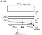
上記の目的を達成するための本発明のGaN系半導体発光素子は、
(A)n型の導電型を有する第1GaN系化合物半導体層、
(B)井戸層、及び、井戸層と井戸層とを隔てる障壁層から成る多重量子井戸構造を有する活性層、及び、
(C)p型の導電型を有する第2GaN系化合物半導体層、
を備えたGaN系半導体発光素子であって、
活性層における第1GaN系化合物半導体層側の井戸層密度をd1、第2GaN系化合物半導体層側の井戸層密度をd2としたとき、d1<d2を満足するように活性層における井戸層が配置されていることを特徴とする。The GaN-based semiconductor light-emitting device of the present invention for achieving the above object is
(A) a first GaN compound semiconductor layer having an n-type conductivity,
(B) an active layer having a multiple quantum well structure comprising a well layer and a barrier layer separating the well layer and the well layer; and
(C) a second GaN compound semiconductor layer having p-type conductivity,
A GaN-based semiconductor light emitting device comprising:
D1 The well layer density of the 1GaN based compound semiconductor layer side in the active layer, when the well layer density of the 2GaN based compound semiconductor layer side was d2, the well in the active layer so as to satisfy d1 <d2 It is characterized in that the layers are arranged.
上記の目的を達成するための本発明の発光装置は、GaN系半導体発光素子と、該GaN系半導体発光素子からの射出光が入射し、GaN系半導体発光素子からの射出光の有する波長と異なる波長を有する光を射出する色変換材料とから成る発光装置であって、
GaN系半導体発光素子は、
(A)n型の導電型を有する第1GaN系化合物半導体層、
(B)井戸層、及び、井戸層と井戸層とを隔てる障壁層から成る多重量子井戸構造を有する活性層、及び、
(C)p型の導電型を有する第2GaN系化合物半導体層、
を備えており、
活性層における第1GaN系化合物半導体層側の井戸層密度をd1、第2GaN系化合物半導体層側の井戸層密度をd2としたとき、d1<d2を満足するように活性層における井戸層が配置されていることを特徴とする。In order to achieve the above object, a light emitting device of the present invention includes a GaN-based semiconductor light-emitting element and light emitted from the GaN-based semiconductor light-emitting element, which is different from the wavelength of the light emitted from the GaN-based semiconductor light-emitting element. A light emitting device comprising a color conversion material that emits light having a wavelength,
GaN-based semiconductor light-emitting elements
(A) a first GaN compound semiconductor layer having an n-type conductivity,
(B) an active layer having a multiple quantum well structure comprising a well layer and a barrier layer separating the well layer and the well layer; and
(C) a second GaN compound semiconductor layer having p-type conductivity,
With
D1 The well layer density of the 1GaN based compound semiconductor layer side in the active layer, when the well layer density of the 2GaN based compound semiconductor layer side was d2, the well in the active layer so as to satisfy d1 <d2 It is characterized in that the layers are arranged.
ここで、本発明の発光装置にあっては、GaN系半導体発光素子からの射出光として、可視光、紫外線、可視光と紫外線の組合せを挙げることができる。 Here, in the light emitting device of the present invention, examples of the light emitted from the GaN-based semiconductor light emitting element include visible light, ultraviolet light, and a combination of visible light and ultraviolet light.
本発明の発光装置にあっては、GaN系半導体発光素子からの射出光は青色であり、色変換材料からの射出光は、黄色、緑色、及び、赤色から成る群から選択された少なくとも1種類の光である構成とすることができる。ここで、GaN系半導体発光素子からの青色の射出光によって励起され、赤色を射出する色変換材料として、具体的には、赤色発光蛍光体粒子、より具体的には、(ME:Eu)S[但し、「ME」は、Ca、Sr及びBaから成る群から選択された少なくとも1種類の原子を意味し、以下においても同様である]、(M:Sm)x(Si,Al)12(O,N)16[但し、「M」は、Li、Mg及びCaから成る群から選択された少なくとも1種類の原子を意味し、以下においても同様である]、ME2Si5N8:Eu、(Ca:Eu)SiN2、(Ca:Eu)AlSiN3を挙げることができる。また、GaN系半導体発光素子からの青色の射出光によって励起され、緑色を射出する色変換材料として、具体的には、緑色発光蛍光体粒子、より具体的には、(ME:Eu)Ga2S4、(M:RE)x(Si,Al)12(O,N)16[但し、「RE」は、Tb及びYbを意味する]、(M:Tb)x(Si,Al)12(O,N)16、(M:Yb)x(Si,Al)12(O,N)16、Si6-ZAlZOZN8-Z:Euを挙げることができる。更には、GaN系半導体発光素子からの青色の射出光によって励起され、黄色を射出する色変換材料として、具体的には、黄色発光蛍光体粒子、より具体的には、YAG(イットリウム・アルミニウム・ガーネット)系蛍光体粒子を挙げることができる。尚、色変換材料は、1種類であってもよいし、2種類以上を混合して用いてもよい。更には、色変換材料を2種類以上を混合して用いることで、黄色、緑色、赤色以外の色の射出光が色変換材料混合品から射出される構成とすることもできる。具体的には、例えば、シアン色を発光する構成としてもよく、この場合には、緑色発光蛍光体粒子(例えば、LaPO4:Ce,Tb、BaMgAl10O17:Eu,Mn、Zn2SiO4:Mn、MgAl11O19:Ce,Tb、Y2SiO5:Ce,Tb、MgAl11O19:CE,Tb,Mn)と青色発光蛍光体粒子(例えば、BaMgAl10O17:Eu、BaMg2Al16O27:Eu、Sr2P2O7:Eu、Sr5(PO4)3Cl:Eu、(Sr,Ca,Ba,Mg)5(PO4)3Cl:Eu、CaWO4、CaWO4:Pb)とを混合したものを用いればよい。In the light emitting device of the present invention, the emitted light from the GaN-based semiconductor light emitting element is blue, and the emitted light from the color conversion material is at least one selected from the group consisting of yellow, green, and red It can be set as the structure which is no light. Here, as a color conversion material that is excited by blue emission light from the GaN-based semiconductor light-emitting element and emits red, specifically, red-emitting phosphor particles, more specifically, (ME: Eu) S. [However, “ME” means at least one kind of atom selected from the group consisting of Ca, Sr and Ba, and the same shall apply hereinafter.) (M: Sm)x (Si, Al)12 ( O, N)16 [However, “M” means at least one atom selected from the group consisting of Li, Mg, and Ca, and the same applies hereinafter.] ME2 Si5 N8 : Eu (Ca: Eu) SiN2 and (Ca: Eu) AlSiN3 . Further, as a color conversion material that is excited by blue light emitted from a GaN-based semiconductor light emitting element and emits green, specifically, green light emitting phosphor particles, more specifically, (ME: Eu) Ga2. S4 , (M: RE)x (Si, Al)12 (O, N)16 [where “RE” means Tb and Yb], (M: Tb)x (Si, Al)12 (O, N) 16, (M : Yb) x (Si, Al) 12 (O, N) 16, Si 6-Z Al Z O Z N 8-Z: Eu may be mentioned. Further, as a color conversion material that is excited by blue light emitted from a GaN-based semiconductor light emitting element and emits yellow, specifically, yellow light emitting phosphor particles, more specifically, YAG (yttrium, aluminum, Garnet) -based phosphor particles. The color conversion material may be one type or a mixture of two or more types. Furthermore, by using a mixture of two or more color conversion materials, it is possible to adopt a configuration in which emitted light of a color other than yellow, green, and red is emitted from the color conversion material mixture. Specifically, for example, it may be configured to emit cyan, and in this case, green phosphor particles (for example, LaPO4 : Ce, Tb, BaMgAl10 O17 : Eu, Mn, Zn2 SiO4). : Mn, MgAl11 O19 : Ce, Tb, Y2 SiO5 : Ce, Tb, MgAl11 O19 : CE, Tb, Mn) and blue-emitting phosphor particles (for example, BaMgAl10 O17 : Eu, BaMg2 Al16 O27 : Eu, Sr2 P2 O7 : Eu, Sr5 (PO4 )3 Cl: Eu, (Sr, Ca, Ba, Mg)5 (PO4 )3 Cl: Eu, CaWO4 , CaWO4 : What mixed Pb) may be used.
GaN系半導体発光素子からの射出光である紫外線である場合、動作電流密度の増加に伴う発光波長のシフトは少ないものの、井戸層密度を規定することで、発光効率の向上、閾値電流の低減を図ることが期待できる。ここで、GaN系半導体発光素子からの射出光である紫外線によって励起され、赤色を射出する色変換材料として、具体的には、赤色発光蛍光体粒子、より具体的には、Y2O3:Eu、YVO4:Eu、Y(P,V)O4:Eu、3.5MgO・0.5MgF2・Ge2:Mn、CaSiO3:Pb,Mn、Mg6AsO11:Mn、(Sr,Mg)3(PO4)3:Sn、La2O2S:Eu、Y2O2S:Euを挙げることができる。また、GaN系半導体発光素子からの射出光である紫外線によって励起され、緑色を射出する色変換材料として、具体的には、緑色発光蛍光体粒子、より具体的には、LaPO4:Ce,Tb、BaMgAl10O17:Eu,Mn、Zn2SiO4:Mn、MgAl11O19:Ce,Tb、Y2SiO5:Ce,Tb、MgAl11O19:CE,Tb,Mn、Si6-ZAlZOZN8-Z:Euを挙げることができる。更には、GaN系半導体発光素子からの射出光である紫外線によって励起され、青色を射出する色変換材料として、具体的には、青色発光蛍光体粒子、より具体的には、BaMgAl10O17:Eu、BaMg2Al16O27:Eu、Sr2P2O7:Eu、Sr5(PO4)3Cl:Eu、(Sr,Ca,Ba,Mg)5(PO4)3Cl:Eu、CaWO4、CaWO4:Pbを挙げることができる。更には、GaN系半導体発光素子からの射出光である紫外線によって励起され、黄色を射出する色変換材料として、具体的には、黄色発光蛍光体粒子、より具体的には、YAG系蛍光体粒子を挙げることができる。尚、色変換材料は、1種類であってもよいし、2種類以上を混合して用いてもよい。更には、色変換材料を2種類以上を混合して用いることで、黄色、緑色、赤色以外の色の射出光が色変換材料混合品から射出される構成とすることもできる。具体的には、シアン色を発光する構成としてもよく、この場合には、上記の緑色発光蛍光体粒子と青色発光蛍光体粒子を混合したものを用いればよい。In the case of ultraviolet light that is emitted from a GaN-based semiconductor light-emitting device, the emission wavelength shifts little with an increase in operating current density, but by defining the well layer density, luminous efficiency is improved and threshold current is reduced. We can expect to plan. Here, as a color conversion material that emits red light by being excited by ultraviolet light that is emitted from the GaN-based semiconductor light-emitting element, specifically, red-emitting phosphor particles, more specifically, Y2 O3 : Eu, YVO4 : Eu, Y (P, V) O4 : Eu, 3.5MgO · 0.5MgF2 · Ge2 : Mn, CaSiO3 : Pb, Mn, Mg6 AsO11 : Mn, (Sr, Mg )3 (PO4 )3 : Sn, La2 O2 S: Eu, Y2 O2 S: Eu. Further, as a color conversion material that emits green light by being excited by ultraviolet light that is light emitted from the GaN-based semiconductor light-emitting element, specifically, green light-emitting phosphor particles, more specifically, LaPO4 : Ce, Tb., BaMgAl 10 O 17: Eu, Mn,
但し、色変換材料は、蛍光粒子に限定されず、例えば、ナノメートルサイズのCdSe/ZnSやナノメートルサイズのシリコンといった量子効果を用いた多色・高効率の発光粒子を挙げることもできるし、半導体材料に添加された希土類原子は殻内遷移により鋭く発光することが知られており、このような技術を適用した発光粒子を挙げることもできる。 However, the color conversion material is not limited to fluorescent particles, and for example, multicolor and high-efficiency luminescent particles using quantum effects such as nanometer-sized CdSe / ZnS and nanometer-sized silicon can be mentioned, It is known that rare earth atoms added to semiconductor materials emit light sharply due to intra-shell transition, and light emitting particles to which such a technique is applied can also be mentioned.
上記の好ましい構成を含む本発明の発光装置にあっては、GaN系半導体発光素子からの射出光と、色変換材料からの射出光(例えば、黄色;赤色及び緑色;黄色及び赤色;緑色、黄色及び赤色)とが混色されて、白色を射出する構成とすることができるが、これに限定するものではなく、可変色照明やディスプレイ応用も可能である。 In the light emitting device of the present invention including the above-described preferred configuration, the light emitted from the GaN-based semiconductor light emitting element and the light emitted from the color conversion material (for example, yellow; red and green; yellow and red; green, yellow) And red) can be mixed to emit white light, but the present invention is not limited to this, and variable color illumination and display applications are also possible.
上記の目的を達成するための本発明の第1の態様に係る画像表示装置は、画像を表示するためのGaN系半導体発光素子を備えた画像表示装置であって、
該GaN系半導体発光素子は、
(A)n型の導電型を有する第1GaN系化合物半導体層、
(B)井戸層、及び、井戸層と井戸層とを隔てる障壁層から成る多重量子井戸構造を有する活性層、及び、
(C)p型の導電型を有する第2GaN系化合物半導体層、
を備えており、
活性層における第1GaN系化合物半導体層側の井戸層密度をd1、第2GaN系化合物半導体層側の井戸層密度をd2としたとき、d1<d2を満足するように活性層における井戸層が配置されていることを特徴とする。An image display device according to a first aspect of the present invention for achieving the above object is an image display device including a GaN-based semiconductor light-emitting element for displaying an image,
The GaN-based semiconductor light-emitting element is
(A) a first GaN compound semiconductor layer having an n-type conductivity,
(B) an active layer having a multiple quantum well structure comprising a well layer and a barrier layer separating the well layer and the well layer; and
(C) a second GaN compound semiconductor layer having p-type conductivity,
With
D1 The well layer density of the 1GaN based compound semiconductor layer side in the active layer, when the well layer density of the 2GaN based compound semiconductor layer side was d2, the well in the active layer so as to satisfy d1 <d2 It is characterized in that the layers are arranged.
ここで、本発明の第1の態様に係る画像表示装置として、例えば、以下に説明する構成、構造の画像表示装置を挙げることができる。尚、特に断りの無い限り、画像表示装置あるいは発光素子パネルを構成するGaN系半導体発光素子の数は、画像表示装置に要求される仕様に基づき、決定すればよい。また、画像表示装置に要求される仕様に基づき、ライト・バルブを更に備えている構成とすることができる。 Here, as the image display apparatus according to the first aspect of the present invention, for example, an image display apparatus having a configuration and structure described below can be cited. Unless otherwise specified, the number of GaN-based semiconductor light-emitting elements constituting the image display device or the light-emitting element panel may be determined based on specifications required for the image display device. Further, based on the specifications required for the image display device, a configuration in which a light valve is further provided can be adopted.
(1)第1Aの態様に係る画像表示装置・・・
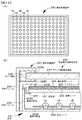
(α)GaN系半導体発光素子が2次元マトリクス状に配列された発光素子パネル、
を備えており、
GaN系半導体発光素子のそれぞれの発光/非発光状態を制御することで、GaN系半導体発光素子の発光状態を直接的に視認させることで画像を表示する、パッシブマトリックスタイプあるいはアクティブマトリックスタイプの直視型の画像表示装置。
(2)第1Bの態様に係る画像表示装置・・・
(α)GaN系半導体発光素子が2次元マトリクス状に配列された発光素子パネル、
を備えており、
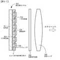
GaN系半導体発光素子のそれぞれの発光/非発光状態を制御し、スクリーンに投影することで画像を表示する、パッシブマトリックスタイプあるいはアクティブマトリックスタイプのプロジェクション型の画像表示装置。
(3)第1Cの態様に係る画像表示装置・・・
(α)赤色を発光する半導体発光素子(例えば、AlGaInP系半導体発光素子やGaN系半導体発光素子。以下においても同様)が2次元マトリクス状に配列された赤色発光素子パネル、
(β)緑色を発光するGaN系半導体発光素子が2次元マトリクス状に配列された緑色発光素子パネル、及び、
(γ)青色を発光するGaN系半導体発光素子が2次元マトリクス状に配列された青色発光素子パネル、並びに、
(δ)赤色発光素子パネル、緑色発光素子パネル及び青色発光素子パネルから射出された光を1本の光路に纏めるための手段(例えば、ダイクロイック・プリズムであり、以下の説明においても同様である)、
を備えており、
赤色発光半導体発光素子、緑色発光GaN系半導体発光素子及び青色発光GaN系半導体発光素子のそれぞれの発光/非発光状態を制御するカラー表示の画像表示装置(直視型あるいはプロジェクション型)。
(4)第1Dの態様に係る画像表示装置・・・
(α)GaN系半導体発光素子、及び、
(β)GaN系半導体発光素子から射出された射出光の通過/非通過を制御するための一種のライト・バルブである光通過制御装置[例えば、液晶表示装置やデジタルマイクロミラーデバイス(DMD)、LCOS(Liquid Crystal On Silicon)であり、以下の説明においても同様である]、
を備えており、
光通過制御装置によってGaN系半導体発光素子から射出された射出光の通過/非通過を制御することで画像を表示する画像表示装置(直視型あるいはプロジェクション型)。尚、GaN系半導体発光素子の数は、画像表示装置に要求される仕様に基づき、決定すればよく、1又は複数とすることができる。また、GaN系半導体発光素子から射出された射出光を光通過制御装置へと案内するための手段(光案内部材)として、導光部材、マイクロレンズアレイ、ミラーや反射板、集光レンズを例示することができる。
(5)第1Eの態様に係る画像表示装置・・・
(α)GaN系半導体発光素子が2次元マトリクス状に配列された発光素子パネル、及び、
(β)GaN系半導体発光素子から射出された射出光の通過/非通過を制御するための光通過制御装置(ライト・バルブ)、
を備えており、
光通過制御装置によってGaN系半導体発光素子から射出された射出光の通過/非通過を制御することで画像を表示する画像表示装置(直視型あるいはプロジェクション型)。
(6)第1Fの態様に係る画像表示装置・・・
(α)赤色を発光する半導体発光素子が2次元マトリクス状に配列された赤色発光素子パネル、及び、赤色発光素子パネルから射出された射出光の通過/非通過を制御するための赤色光通過制御装置(ライト・バルブ)、
(β)緑色を発光するGaN系半導体発光素子が2次元マトリクス状に配列された緑色発光素子パネル、及び、緑色発光素子パネルから射出された射出光の通過/非通過を制御するための緑色光通過制御装置(ライト・バルブ)、
(γ)青色を発光するGaN系半導体発光素子が2次元マトリクス状に配列された青色発光素子パネル、及び、青色発光素子パネルから射出された射出光の通過/非通過を制御するための青色光通過制御装置(ライト・バルブ)、並びに、
(δ)赤色光通過制御装置、緑色光通過制御装置及び青色光通過制御装置を通過した光を1本の光路に纏めるための手段、
を備えており、
光通過制御装置によってこれらの発光素子パネルから射出された射出光の通過/非通過を制御することで画像を表示するカラー表示の画像表示装置(直視型あるいはプロジェクション型)。
(7)第1Gの態様に係る画像表示装置・・・
(α)赤色を発光する半導体発光素子、
(β)緑色を発光するGaN系半導体発光素子、及び、
(γ)青色を発光するGaN系半導体発光素子、並びに、
(δ)赤色発光半導体発光素子、緑色発光GaN系半導体発光素子及び青色発光GaN系半導体発光素子のそれぞれから射出された光を1本の光路に纏めるための手段、更には、
(ε)1本の光路に纏めるための手段から射出された光の通過/非通過を制御するための光通過制御装置(ライト・バルブ)、
を備えており、
光通過制御装置によってこれらの発光素子から射出された射出光の通過/非通過を制御することで画像を表示する、フィールドシーケンシャル方式のカラー表示の画像表示装置(直視型あるいはプロジェクション型)。
(8)第1Hの態様に係る画像表示装置・・・
(α)赤色を発光する半導体発光素子が2次元マトリクス状に配列された赤色発光素子パネル、
(β)緑色を発光するGaN系半導体発光素子が2次元マトリクス状に配列された緑色発光素子パネル、及び、
(γ)青色を発光するGaN系半導体発光素子が2次元マトリクス状に配列された青色発光素子パネル、並びに、
(δ)赤色発光素子パネル、緑色発光素子パネル及び青色発光素子パネルのそれぞれから射出された光を1本の光路に纏めるための手段、更には、
(ε)1本の光路に纏めるための手段から射出された光の通過/非通過を制御するための光通過制御装置(ライト・バルブ)、
を備えており、
光通過制御装置によってこれらの発光素子パネルから射出された射出光の通過/非通過を制御することで画像を表示する、フィールドシーケンシャル方式のカラー表示の画像表示装置(直視型あるいはプロジェクション型)。(1) Image display device according to aspect 1A ...
(Α) a light emitting element panel in which GaN-based semiconductor light emitting elements are arranged in a two-dimensional matrix;
With
Passive matrix type or active matrix type direct view type that displays the image by directly viewing the light emission state of the GaN-based semiconductor light-emitting device by controlling the light emission / non-light-emitting state of each GaN-based semiconductor light-emitting device Image display device.
(2) Image display device according to
(Α) a light emitting element panel in which GaN-based semiconductor light emitting elements are arranged in a two-dimensional matrix;
With
A projection type image display device of a passive matrix type or an active matrix type that displays an image by controlling the light emitting / non-emitting state of each GaN-based semiconductor light emitting element and projecting it onto a screen.
(3) Image display device according to aspect 1C ...
(Α) a red light-emitting element panel in which semiconductor light-emitting elements that emit red light (for example, AlGaInP-based semiconductor light-emitting elements and GaN-based semiconductor light-emitting elements; the same applies to the following) are arranged in a two-dimensional matrix;
(Β) a green light-emitting element panel in which GaN-based semiconductor light-emitting elements emitting green light are arranged in a two-dimensional matrix, and
(Γ) a blue light emitting element panel in which GaN-based semiconductor light emitting elements emitting blue light are arranged in a two-dimensional matrix, and
(Δ) Means for collecting light emitted from the red light emitting element panel, the green light emitting element panel, and the blue light emitting element panel into one optical path (for example, a dichroic prism, the same applies in the following description) ,
With
A color display image display device (direct view type or projection type) for controlling the light emitting / non-light emitting state of each of a red light emitting semiconductor light emitting element, a green light emitting GaN semiconductor light emitting element, and a blue light emitting GaN semiconductor light emitting element.
(4) Image display device according to aspect 1D ...
(Α) a GaN-based semiconductor light emitting device, and
(Β) A light passage control device which is a kind of light valve for controlling passage / non-passage of light emitted from a GaN-based semiconductor light emitting device [for example, a liquid crystal display device, a digital micromirror device (DMD), LCOS (Liquid Crystal On Silicon), and the same applies to the following description.]
With
An image display device (direct view type or projection type) that displays an image by controlling passage / non-passage of light emitted from a GaN-based semiconductor light-emitting element by a light passage control device. The number of GaN-based semiconductor light-emitting elements may be determined based on specifications required for the image display device, and may be one or more. Examples of means (light guide member) for guiding the emitted light emitted from the GaN-based semiconductor light emitting device to the light passage control device include a light guide member, a microlens array, a mirror, a reflector, and a condenser lens. can do.
(5) Image display device according to aspect 1E ...
(Α) a light-emitting element panel in which GaN-based semiconductor light-emitting elements are arranged in a two-dimensional matrix, and
(Β) a light passage control device (light valve) for controlling passage / non-passage of the light emitted from the GaN-based semiconductor light-emitting element;
With
An image display device (direct view type or projection type) that displays an image by controlling passage / non-passage of light emitted from a GaN-based semiconductor light-emitting element by a light passage control device.
(6) Image display device according to aspect 1F ...
(Α) A red light emitting element panel in which semiconductor light emitting elements emitting red light are arranged in a two-dimensional matrix, and a red light passage control for controlling passage / non-passage of the emitted light emitted from the red light emitting element panel Equipment (light valve),
(Β) A green light emitting element panel in which GaN-based semiconductor light emitting elements emitting green light are arranged in a two-dimensional matrix, and green light for controlling passage / non-passage of the emitted light emitted from the green light emitting element panel Passage control device (light valve),
(Γ) Blue light emitting element panel in which GaN-based semiconductor light emitting elements emitting blue light are arranged in a two-dimensional matrix, and blue light for controlling passage / non-passage of the emitted light emitted from the blue light emitting element panel A passage control device (light valve), and
(Δ) means for collecting light that has passed through the red light passage control device, the green light passage control device, and the blue light passage control device into one optical path;
With
A color display image display device (direct view type or projection type) that displays an image by controlling passage / non-passage of light emitted from these light emitting element panels by a light passage control device.
(7) Image display device according to 1G aspect ...
(Α) a semiconductor light emitting element that emits red light;
(Β) a GaN-based semiconductor light-emitting element that emits green light, and
(Γ) a GaN-based semiconductor light emitting device that emits blue light, and
(Δ) means for collecting light emitted from each of the red light emitting semiconductor light emitting device, the green light emitting GaN semiconductor light emitting device, and the blue light emitting GaN semiconductor light emitting device into one optical path;
(Ε) a light passage control device (light valve) for controlling the passage / non-passage of the light emitted from the means for collecting in one light path;
With
A field-sequential color display image display device (direct view type or projection type) that displays an image by controlling passage / non-passage of light emitted from these light emitting elements by a light passage control device.
(8) Image display device according to aspect 1H ...
(Α) a red light emitting element panel in which semiconductor light emitting elements emitting red light are arranged in a two-dimensional matrix;
(Β) a green light-emitting element panel in which GaN-based semiconductor light-emitting elements emitting green light are arranged in a two-dimensional matrix, and
(Γ) a blue light emitting element panel in which GaN-based semiconductor light emitting elements emitting blue light are arranged in a two-dimensional matrix, and
(Δ) means for collecting the light emitted from each of the red light emitting element panel, the green light emitting element panel, and the blue light emitting element panel into one optical path;
(Ε) a light passage control device (light valve) for controlling the passage / non-passage of the light emitted from the means for collecting in one light path;
With
A field sequential color display image display device (direct view type or projection type) that displays an image by controlling passage / non-passage of the light emitted from these light emitting element panels by a light passage control device.
また、上記の目的を達成するための本発明の第2の態様に係る画像表示装置は、青色を発光する第1発光素子、緑色を発光する第2発光素子、及び、赤色を発光する第3発光素子から構成された、カラー画像を表示するための発光素子ユニットが、2次元マトリクス状に配列されて成る画像表示装置であって、
第1発光素子、第2発光素子及び第3発光素子の内の少なくとも1つの発光素子を構成するGaN系半導体発光素子は、
(A)n型の導電型を有する第1GaN系化合物半導体層、
(B)井戸層、及び、井戸層と井戸層とを隔てる障壁層から成る多重量子井戸構造を有する活性層、及び、
(C)p型の導電型を有する第2GaN系化合物半導体層、
を備えており、
活性層における第1GaN系化合物半導体層側の井戸層密度をd1、第2GaN系化合物半導体層側の井戸層密度をd2としたとき、d1<d2を満足するように活性層における井戸層が配置されていることを特徴とする。The image display device according to the second aspect of the present invention for achieving the above object includes a first light emitting element that emits blue light, a second light emitting element that emits green light, and a third light emitting light that emits red light. An image display device comprising light emitting element units configured to display a color image, the light emitting element units being arranged in a two-dimensional matrix,
A GaN-based semiconductor light-emitting element constituting at least one of the first light-emitting element, the second light-emitting element, and the third light-emitting element,
(A) a first GaN compound semiconductor layer having an n-type conductivity,
(B) an active layer having a multiple quantum well structure comprising a well layer and a barrier layer separating the well layer and the well layer; and
(C) a second GaN compound semiconductor layer having p-type conductivity,
With
D1 The well layer density of the 1GaN based compound semiconductor layer side in the active layer, when the well layer density of the 2GaN based compound semiconductor layer side was d2, the well in the active layer so as to satisfy d1 <d2 It is characterized in that the layers are arranged.
ここで、本発明の第2の態様に係る画像表示装置として、例えば、以下に説明する構成、構造の画像表示装置を挙げることができる。尚、発光素子ユニットの数は、画像表示装置に要求される仕様に基づき、決定すればよい。また、画像表示装置に要求される仕様に基づき、ライト・バルブを更に備えている構成とすることができる。 Here, examples of the image display apparatus according to the second aspect of the present invention include an image display apparatus having a configuration and structure described below. The number of light emitting element units may be determined based on specifications required for the image display device. Further, based on the specifications required for the image display device, a configuration in which a light valve is further provided can be adopted.
(1)第2Aの態様に係る画像表示装置・・・
第1発光素子、第2発光素子及び第3発光素子のそれぞれの発光/非発光状態を制御することで、各発光素子の発光状態を直接的に視認させることで画像を表示する、パッシブマトリックスタイプあるいはアクティブマトリックスタイプの直視型、カラー表示の画像表示装置。
(2)第2Bの態様に係る画像表示装置・・・
第1発光素子、第2発光素子及び第3発光素子のそれぞれの発光/非発光状態を制御し、スクリーンに投影することで画像を表示する、パッシブマトリックスタイプあるいはアクティブマトリックスタイプのプロジェクション型、カラー表示の画像表示装置。
(3)第2Cの態様に係る画像表示装置・・・
2次元マトリクス状に配列された発光素子ユニットからの射出光の通過/非通過を制御するための光通過制御装置(ライト・バルブ)を備えており、発光素子ユニットにおける第1発光素子、第2発光素子及び第3発光素子のそれぞれの発光/非発光状態を時分割制御し、更に、光通過制御装置によって第1発光素子、第2発光素子及び第3発光素子から射出された射出光の通過/非通過を制御することで画像を表示する、フィールドシーケンシャル方式のカラー表示の画像表示装置(直視型あるいはプロジェクション型)。(1) Image display device according to aspect 2A ...
A passive matrix type that displays an image by directly viewing the light emitting state of each light emitting element by controlling the light emitting / non-light emitting state of each of the first light emitting element, the second light emitting element, and the third light emitting element. Alternatively, an active matrix type direct-view type color display image display device.
(2) Image display apparatus according to aspect 2B ...
Control the light emitting / non-light emitting state of each of the first light emitting element, the second light emitting element, and the third light emitting element, and project the image onto the screen to display an image, a passive matrix type or active matrix type projection type, color display Image display device.
(3) Image display device according to aspect 2C ...
A light passage control device (light valve) for controlling passage / non-passage of light emitted from the light emitting element units arranged in a two-dimensional matrix is provided, and includes a first light emitting element and a second light emitting element in the light emitting element unit. The light emitting / non-light emitting state of each of the light emitting element and the third light emitting element is controlled in a time-sharing manner, and the light passing through the first light emitting element, the second light emitting element, and the third light emitting element is passed by the light passage control device. / Field sequential color display image display device (direct view type or projection type) that displays images by controlling non-passage.
上記の目的を達成するための本発明の面状光源装置は、透過型あるいは半透過型の液晶表示装置を背面から照射する面状光源装置であって、
面状光源装置に備えられた光源としてのGaN系半導体発光素子は、
(A)n型の導電型を有する第1GaN系化合物半導体層、
(B)井戸層、及び、井戸層と井戸層とを隔てる障壁層から成る多重量子井戸構造を有する活性層、及び、
(C)p型の導電型を有する第2GaN系化合物半導体層、
を備えており、
活性層における第1GaN系化合物半導体層側の井戸層密度をd1、第2GaN系化合物半導体層側の井戸層密度をd2としたとき、d1<d2を満足するように活性層における井戸層が配置されていることを特徴とする。To achieve the above object, a planar light source device of the present invention is a planar light source device that irradiates a transmissive or transflective liquid crystal display device from the back,
A GaN-based semiconductor light-emitting element as a light source provided in a planar light source device is
(A) a first GaN compound semiconductor layer having an n-type conductivity,
(B) an active layer having a multiple quantum well structure comprising a well layer and a barrier layer separating the well layer and the well layer; and
(C) a second GaN compound semiconductor layer having p-type conductivity,
With
D1 The well layer density of the 1GaN based compound semiconductor layer side in the active layer, when the well layer density of the 2GaN based compound semiconductor layer side was d2, the well in the active layer so as to satisfy d1 <d2 It is characterized in that the layers are arranged.
上記の目的を達成するための本発明の液晶表示装置組立体は、透過型あるいは半透過型の液晶表示装置、及び、該液晶表示装置を背面から照射する面状光源装置を備えた液晶表示装置組立体であって、
面状光源装置に備えられた光源としてのGaN系半導体発光素子は、
(A)n型の導電型を有する第1GaN系化合物半導体層、
(B)井戸層、及び、井戸層と井戸層とを隔てる障壁層から成る多重量子井戸構造を有する活性層、及び、
(C)p型の導電型を有する第2GaN系化合物半導体層、
を備えており、
活性層における第1GaN系化合物半導体層側の井戸層密度をd1、第2GaN系化合物半導体層側の井戸層密度をd2としたとき、d1<d2を満足するように活性層における井戸層が配置されていることを特徴とする。In order to achieve the above object, a liquid crystal display device assembly of the present invention includes a transmissive or transflective liquid crystal display device and a liquid crystal display device including a planar light source device that irradiates the liquid crystal display device from the back side. An assembly comprising:
A GaN-based semiconductor light-emitting element as a light source provided in a planar light source device is
(A) a first GaN compound semiconductor layer having an n-type conductivity,
(B) an active layer having a multiple quantum well structure comprising a well layer and a barrier layer separating the well layer and the well layer; and
(C) a second GaN compound semiconductor layer having p-type conductivity,
With
D1 The well layer density of the 1GaN based compound semiconductor layer side in the active layer, when the well layer density of the 2GaN based compound semiconductor layer side was d2, the well in the active layer so as to satisfy d1 <d2 It is characterized in that the layers are arranged.
本発明の面状光源装置にあっては、また、本発明の液晶表示装置組立体における面状光源装置にあっては、光源は、青色を発光する第1発光素子、緑色を発光する第2発光素子、及び、赤色を発光する第3発光素子を備えており、GaN系半導体発光素子は、第1発光素子、第2発光素子及び第3発光素子の内の少なくとも1つ(1種類)の発光素子を構成する態様とすることができるが、これに限定するものではなく、面状光源装置における光源を1又は複数の本発明の発光装置から構成することもできる。また、第1発光素子、第2発光素子、及び、第3発光素子は、それぞれ、1つであってもよいし、複数であってもよい。 In the planar light source device of the present invention, and in the planar light source device in the liquid crystal display device assembly of the present invention, the light source is a first light emitting element that emits blue light, and a second light source that emits green light. A light-emitting element and a third light-emitting element that emits red light. The GaN-based semiconductor light-emitting element includes at least one (one type) of the first light-emitting element, the second light-emitting element, and the third light-emitting element. Although it can be set as the aspect which comprises a light emitting element, it is not limited to this, The light source in a planar light source device can also be comprised from the light-emitting device of 1 or several this invention. In addition, the number of the first light emitting element, the second light emitting element, and the third light emitting element may be one or plural, respectively.
本発明の第2の態様に係る画像表示装置、本発明の面状光源装置、あるいは、本発明の液晶表示装置組立体において、光源を第1発光素子、第2発光素子及び第3発光素子から構成する場合、第1発光素子、第2発光素子及び第3発光素子の内の少なくとも1つ(1種類)の発光素子はGaN系半導体発光素子によって構成される。云い換えれば、第1発光素子、第2発光素子及び第3発光素子の内のいずれか1種類の発光素子はGaN系半導体発光素子から構成され、残りの2種類の発光素子は他の構成の半導体発光素子から構成されていてもよいし、第1発光素子、第2発光素子及び第3発光素子の内のいずれか2種類の発光素子はGaN系半導体発光素子から構成され、残りの1種類の発光素子は他の構成の半導体発光素子から構成されていてもよいし、第1発光素子、第2発光素子及び第3発光素子の全ての発光素子がGaN系半導体発光素子から構成されていてもよい。尚、他の構成の半導体発光素子として、赤色を発光するAlGaInP系半導体発光素子を挙げることができる。 In the image display device according to the second aspect of the present invention, the planar light source device of the present invention, or the liquid crystal display device assembly of the present invention, the light source is changed from the first light emitting element, the second light emitting element, and the third light emitting element. When configured, at least one (one type) of the first light emitting element, the second light emitting element, and the third light emitting element is composed of a GaN-based semiconductor light emitting element. In other words, any one of the first light-emitting element, the second light-emitting element, and the third light-emitting element is formed of a GaN-based semiconductor light-emitting element, and the remaining two types of light-emitting elements have other configurations. The light emitting element may be composed of a semiconductor light emitting element, or any one of the first light emitting element, the second light emitting element, and the third light emitting element is composed of a GaN-based semiconductor light emitting element, and the remaining one type The light emitting element may be composed of a semiconductor light emitting element of another configuration, or all of the light emitting elements of the first light emitting element, the second light emitting element, and the third light emitting element are composed of a GaN-based semiconductor light emitting element. Also good. An example of a semiconductor light emitting device having another configuration is an AlGaInP semiconductor light emitting device that emits red light.
本発明の面状光源装置、あるいは、本発明の液晶表示装置組立体における面状光源装置は、2種類の面状光源装置(バックライト)、即ち、例えば実開昭63−187120や特開2002−277870に開示された直下型の面状光源装置、並びに、例えば特開2002−131552に開示されたエッジライト型(サイドライト型とも呼ばれる)の面状光源装置とすることができる。尚、GaN系半導体発光素子の数は本質的に任意であり、面状光源装置に要求される仕様に基づき決定すればよい。 The planar light source device of the present invention or the planar light source device in the liquid crystal display device assembly of the present invention has two types of planar light source devices (backlights), for example, Japanese Utility Model Laid-Open Nos. 63-187120 and 2002. The direct-type planar light source device disclosed in JP-A-277870 and the edge light type (also referred to as sidelight type) planar light source device disclosed in, for example, JP-A-2002-131552 can be used. Note that the number of GaN-based semiconductor light-emitting elements is essentially arbitrary, and may be determined based on specifications required for the planar light source device.
ここで、直下型の面状光源装置にあっては、液晶表示装置に対向して、第1発光素子、第2発光素子及び第3発光素子が配置され、液晶表示装置と第1発光素子、第2発光素子及び第3発光素子との間には、拡散板、拡散シート、プリズムシート、偏光変換シートといった光学機能シート群や、反射シートが配置されている。 Here, in the direct type planar light source device, the first light emitting element, the second light emitting element, and the third light emitting element are arranged facing the liquid crystal display device, and the liquid crystal display device, the first light emitting element, Between the second light emitting element and the third light emitting element, an optical function sheet group such as a diffusion plate, a diffusion sheet, a prism sheet, and a polarization conversion sheet, and a reflection sheet are arranged.
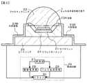
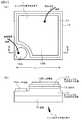
直下型の面状光源装置にあっては、より具体的には、赤色(例えば、波長640nm)を発光する半導体発光素子、緑色(例えば、波長530nm)を発光するGaN系半導体発光素子、及び、青色(例えば、波長450nm)を発光するGaN系半導体発光素子が、筐体内に配置、配列されている構成とすることができるが、これに限定するものではない。ここで、複数の赤色を発光する半導体発光素子、複数の緑色を発光するGaN系半導体発光素子、及び、複数の青色を発光するGaN系半導体発光素子が、筐体内に配置、配列されている場合、これらの発光素子の配列状態として、赤色発光の半導体発光素子、緑色発光のGaN系半導体発光素子及び青色発光のGaN系半導体発光素子を1組とした発光素子列を液晶表示装置の画面水平方向に複数、連ねて発光素子列アレイを形成し、この発光素子列アレイを液晶表示装置の画面垂直方向に複数本、並べる配列を例示することができる。尚、発光素子列として、(1つの赤色発光の半導体発光素子,1つの緑色発光のGaN系半導体発光素子,1つの青色発光のGaN系半導体発光素子)、(1つの赤色発光の半導体発光素子,2つの緑色発光のGaN系半導体発光素子,1つの青色発光のGaN系半導体発光素子)、(2つの赤色発光の半導体発光素子,2つの緑色発光のGaN系半導体発光素子,1つの青色発光のGaN系半導体発光素子)等の複数個の組合せを挙げることができる。尚、赤色、緑色、青色以外の第4番目の色を発光する発光素子を更に備えていてもよい。また、GaN系半導体発光素子には、例えば、日経エレクトロニクス 2004年12月20日第889号の第128ページに掲載されたような光取出しレンズが取り付けられていてもよい。 In the direct-type planar light source device, more specifically, a semiconductor light emitting element that emits red light (for example, wavelength 640 nm), a GaN-based semiconductor light emitting element that emits green light (for example,
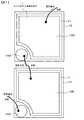
一方、エッジライト型の面状光源装置にあっては、液晶表示装置に対向して導光板が配置され、導光板の側面(次に述べる第1側面)にGaN系半導体発光素子が配置される。導光板は、第1面(底面)、この第1面と対向した第2面(頂面)、第1側面、第2側面、第1側面と対向した第3側面、及び、第2側面と対向した第4側面を有する。導光板のより具体的な形状として、全体として、楔状の切頭四角錐形状を挙げることができ、この場合、切頭四角錐の2つの対向する側面が第1面及び第2面に相当し、切頭四角錐の底面が第1側面に相当する。そして、第1面(底面)の表面部には凸部及び/又は凹部が設けられていることが望ましい。導光板の第1側面から光が入射され、第2面(頂面)から液晶表示装置に向けて光が射出される。ここで、導光板の第2面は、平滑としてもよいし(即ち、鏡面としてもよいし)、拡散効果のあるブラストシボを設けてもよい(即ち、微細な凹凸面とすることもできる)。 On the other hand, in the edge light type planar light source device, a light guide plate is disposed facing the liquid crystal display device, and a GaN-based semiconductor light emitting element is disposed on a side surface (first side surface described below) of the light guide plate. . The light guide plate includes a first surface (bottom surface), a second surface (top surface) facing the first surface, a first side surface, a second side surface, a third side surface facing the first side surface, and a second side surface. It has the 4th side which countered. As a more specific shape of the light guide plate, a wedge-shaped truncated quadrangular pyramid shape can be cited as a whole. In this case, two opposing side surfaces of the truncated quadrangular pyramid correspond to the first surface and the second surface. The bottom surface of the truncated quadrangular pyramid corresponds to the first side surface. And it is desirable for the surface part of the 1st surface (bottom surface) to provide the convex part and / or the recessed part. Light is incident from the first side surface of the light guide plate, and light is emitted from the second surface (top surface) toward the liquid crystal display device. Here, the second surface of the light guide plate may be smooth (that is, may be a mirror surface), or may be provided with a blast texture having a diffusion effect (that is, a fine uneven surface).
導光板の第1面(底面)には、凸部及び/又は凹部が設けられていることが望ましい。即ち、導光板の第1面には、凸部が設けられ、あるいは又、凹部が設けられ、あるいは又、凹凸部が設けられていることが望ましい。凹凸部が設けられている場合、凹部と凸部とが連続していてもよいし、不連続であってもよい。導光板の第1面に設けられた凸部及び/又は凹部は、導光板への光入射方向と所定の角度を成す方向に沿って延びる連続した凸部及び/又は凹部である構成とすることができる。このような構成にあっては、導光板への光入射方向であって第1面と垂直な仮想平面で導光板を切断したときの連続した凸形状あるいは凹形状の断面形状として、三角形;正方形、長方形、台形を含む任意の四角形;任意の多角形;円形、楕円形、放物線、双曲線、カテナリー等を含む任意の滑らかな曲線を例示することができる。尚、導光板への光入射方向と所定の角度を成す方向とは、導光板への光入射方向を0度としたとき、60度〜120度の方向を意味する。以下においても同様である。あるいは又、導光板の第1面に設けられた凸部及び/又は凹部は、導光板への光入射方向と所定の角度を成す方向に沿って延びる不連続の凸部及び/又は凹部である構成とすることができる。このような構成にあっては、不連続の凸形状あるいは凹形状の形状として、角錐、円錐、円柱、三角柱や四角柱を含む多角柱、球の一部、回転楕円体の一部、回転放物線体の一部、回転双曲線体の一部といった各種の滑らかな曲面を例示することができる。尚、導光板において、場合によっては、第1面の周縁部には凸部や凹部が形成されていなくともよい。更には、光源から射出され、導光板に入射した光が導光板の第1面に形成された凸部あるいは凹部に衝突して散乱されるが、導光板の第1面に設けられた凸部あるいは凹部の高さや深さ、ピッチ、形状を、一定としてもよいし、光源から離れるに従い変化させてもよい。後者の場合、例えば凸部あるいは凹部のピッチを光源から離れるに従い細かくしてもよい。ここで、凸部のピッチ、あるいは、凹部のピッチとは、導光板への光入射方向に沿った凸部のピッチ、あるいは、凹部のピッチを意味する。 It is desirable that the first surface (bottom surface) of the light guide plate is provided with a convex portion and / or a concave portion. That is, it is desirable that the first surface of the light guide plate is provided with a convex portion, or a concave portion, or an uneven portion. When the concavo-convex portion is provided, the concave portion and the convex portion may be continuous or discontinuous. The convex portions and / or concave portions provided on the first surface of the light guide plate are configured to be continuous convex portions and / or concave portions extending along a direction forming a predetermined angle with the light incident direction to the light guide plate. Can do. In such a configuration, a triangle or square is used as a continuous convex or concave cross-sectional shape when the light guide plate is cut in a virtual plane perpendicular to the first surface in the light incident direction to the light guide plate. Any smooth curve can be exemplified, including any rectangle, including rectangle, trapezoid; any polygon; circle, ellipse, parabola, hyperbola, catenary and the like. The direction forming a predetermined angle with the light incident direction on the light guide plate means a direction of 60 to 120 degrees when the light incident direction on the light guide plate is 0 degree. The same applies to the following. Alternatively, the convex portion and / or concave portion provided on the first surface of the light guide plate is a discontinuous convex portion and / or concave portion extending along a direction forming a predetermined angle with the light incident direction to the light guide plate. It can be configured. In such a configuration, as a discontinuous convex shape or concave shape, a pyramid, a cone, a cylinder, a polygonal column including a triangular column or a quadrangular column, a part of a sphere, a part of a spheroid, a rotating parabola Various smooth curved surfaces such as a part of a body and a part of a rotating hyperbola can be exemplified. In the light guide plate, in some cases, a convex portion or a concave portion may not be formed on the peripheral portion of the first surface. Furthermore, the light emitted from the light source and incident on the light guide plate collides with the convex portion or concave portion formed on the first surface of the light guide plate and is scattered, but the convex portion provided on the first surface of the light guide plate. Alternatively, the height, depth, pitch, and shape of the recesses may be constant or may be changed as the distance from the light source increases. In the latter case, for example, the pitch of the convex portion or the concave portion may be made finer as the distance from the light source increases. Here, the pitch of the convex portions or the pitch of the concave portions means the pitch of the convex portions or the pitch of the concave portions along the light incident direction to the light guide plate.
導光板を備えた面状光源装置にあっては、導光板の第1面に対向して反射部材を配置することが望ましい。導光板の第2面に対向して液晶表示装置が配置されている。光源から射出された光は、導光板の第1側面(例えば、切頭四角錐の底面に相当する面)から導光板に入射し、第1面の凸部あるいは凹部に衝突して散乱され、第1面から射出し、反射部材にて反射され、第1面に再び入射し、第2面から射出され、液晶表示装置を照射する。液晶表示装置と導光板の第2面との間に、例えば、拡散シートやプリズムシートを配置してもよい。また、光源から射出された光を直接、導光板に導いてもよいし、間接的に導光板に導いてもよい。後者の場合、例えば、光ファイバーを用いればよい。 In the planar light source device including the light guide plate, it is desirable to dispose the reflection member so as to face the first surface of the light guide plate. A liquid crystal display device is disposed to face the second surface of the light guide plate. The light emitted from the light source enters the light guide plate from the first side surface of the light guide plate (for example, the surface corresponding to the bottom surface of the truncated quadrangular pyramid), collides with the convex portion or the concave portion of the first surface, and is scattered. The light is emitted from the first surface, is reflected by the reflecting member, is incident on the first surface again, is emitted from the second surface, and irradiates the liquid crystal display device. For example, a diffusion sheet or a prism sheet may be disposed between the liquid crystal display device and the second surface of the light guide plate. Further, the light emitted from the light source may be guided directly to the light guide plate or indirectly guided to the light guide plate. In the latter case, for example, an optical fiber may be used.
導光板は、光源が射出する光を余り吸収することの無い材料から導光板を作製することが好ましい。具体的には、導光板を構成する材料として、例えば、ガラスや、プラスチック材料(例えば、PMMA、ポリカーボネート樹脂、アクリル系樹脂、非晶性のポリプロピレン系樹脂、AS樹脂を含むスチレン系樹脂)を挙げることができる。 The light guide plate is preferably made of a material that does not absorb much light emitted from the light source. Specifically, examples of the material constituting the light guide plate include glass and plastic materials (for example, PMMA, polycarbonate resin, acrylic resin, amorphous polypropylene resin, and styrene resin including AS resin). be able to.
例えば、透過型のカラー液晶表示装置は、例えば、透明第1電極を備えたフロント・パネル、透明第2電極を備えたリア・パネル、及び、フロント・パネルとリア・パネルとの間に配された液晶材料から成る。 For example, a transmissive color liquid crystal display device is disposed, for example, between a front panel having a transparent first electrode, a rear panel having a transparent second electrode, and a front panel and a rear panel. Made of liquid crystal material.
ここで、フロント・パネルは、より具体的には、例えば、ガラス基板やシリコン基板から成る第1の基板と、第1の基板の内面に設けられた透明第1電極(共通電極とも呼ばれ、例えば、ITOから成る)と、第1の基板の外面に設けられた偏光フィルムとから構成されている。更には、フロント・パネルは、第1の基板の内面に、アクリル樹脂やエポキシ樹脂から成るオーバーコート層によって被覆されたカラーフィルターが設けられ、オーバーコート層上に透明第1電極が形成された構成を有している。透明第1電極上には配向膜が形成されている。カラーフィルターの配置パターンとして、デルタ配列、ストライプ配列、ダイアゴナル配列、レクタングル配列を挙げることができる。一方、リア・パネルは、より具体的には、例えば、ガラス基板やシリコン基板から成る第2の基板と、第2の基板の内面に形成されたスイッチング素子と、スイッチング素子によって導通/非導通が制御される透明第2電極(画素電極とも呼ばれ、例えば、ITOから成る)と、第2の基板の外面に設けられた偏光フィルムとから構成されている。透明第2電極を含む全面には配向膜が形成されている。これらの透過型のカラー液晶表示装置を構成する各種の部材や液晶材料は、周知の部材、材料から構成することができる。尚、スイッチング素子として、単結晶シリコン半導体基板に形成されたMOS型FETや薄膜トランジスタ(TFT)といった3端子素子や、MIM素子、バリスタ素子、ダイオード等の2端子素子を例示することができる。 Here, more specifically, the front panel is, for example, a first substrate made of a glass substrate or a silicon substrate, and a transparent first electrode (also called a common electrode) provided on the inner surface of the first substrate. For example, it is made of ITO) and a polarizing film provided on the outer surface of the first substrate. Furthermore, the front panel has a configuration in which a color filter covered with an overcoat layer made of acrylic resin or epoxy resin is provided on the inner surface of the first substrate, and a transparent first electrode is formed on the overcoat layer. have. An alignment film is formed on the transparent first electrode. Examples of the color filter arrangement pattern include a delta arrangement, a stripe arrangement, a diagonal arrangement, and a rectangle arrangement. On the other hand, the rear panel more specifically includes, for example, a second substrate made of a glass substrate or a silicon substrate, a switching element formed on the inner surface of the second substrate, and conduction / non-conduction by the switching element. A transparent second electrode to be controlled (also called a pixel electrode, which is made of, for example, ITO) and a polarizing film provided on the outer surface of the second substrate. An alignment film is formed on the entire surface including the transparent second electrode. Various members and liquid crystal materials constituting these transmissive color liquid crystal display devices can be composed of known members and materials. Examples of the switching element include a three-terminal element such as a MOS type FET and a thin film transistor (TFT) formed on a single crystal silicon semiconductor substrate, and a two-terminal element such as an MIM element, a varistor element, and a diode.
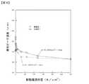
以上に説明した好ましい形態、構成を含む本発明のGaN系半導体発光素子、発光装置、第1の態様あるいは第2の態様に係る画像表示装置、面状光源装置、あるいは、液晶表示装置組立体(以下、これらを総称して、単に、本発明と呼ぶ場合がある)において、動作電流密度を30A/cm2としたときの活性層の発光波長をλ2(nm)、動作電流密度を300A/cm2としたときの活性層の発光波長をλ3(nm)とするとき、
500(nm)≦λ2≦550(nm)
0≦|λ2−λ3|≦5(nm)
を満足することが望ましく、あるいは又、動作電流密度を1A/cm2としたときの活性層の発光波長をλ1(nm)、動作電流密度を30A/cm2としたときの活性層の発光波長をλ2(nm)、動作電流密度を300A/cm2としたときの活性層の発光波長をλ3(nm)とするとき、
500(nm)≦λ2≦550(nm)
0≦|λ1−λ2|≦10(nm)
0≦|λ2−λ3|≦5(nm)
を満足することが望ましい。The GaN-based semiconductor light-emitting device, light-emitting device, image display device, planar light source device, or liquid crystal display device assembly according to the first or second aspect of the present invention including the preferred embodiments and configurations described above ( Hereinafter, these may be collectively referred to simply as the present invention), and the emission wavelength of the active layer when the operating current density is 30 A / cm2 is λ2 (nm), and the operating current density is 300 A / cm2. When the emission wavelength of the active layer when it is cm2 is λ3 (nm),
500 (nm) ≦ λ2 ≦ 550 (nm)
0 ≦ | λ2 −λ3 | ≦ 5 (nm)
It is desirable to satisfy the, or alternatively, the emission wavelength of the active layer when the operating current density1A / cm 2 λ 1 (nm ), emission of the active layer when the operating current density was 30A / cm2 When the emission wavelength of the active layer when the wavelength is λ2 (nm) and the operating current density is 300 A / cm2 is λ3 (nm),
500 (nm) ≦ λ2 ≦ 550 (nm)
0 ≦ | λ1 −λ2 | ≦ 10 (nm)
0 ≦ | λ2 −λ3 | ≦ 5 (nm)
It is desirable to satisfy
あるいは又、上記の好ましい構成を含む本発明において、動作電流密度を30A/cm2としたときの活性層の発光波長をλ2(nm)、動作電流密度を300A/cm2としたときの活性層の発光波長をλ3(nm)とするとき、
430(nm)≦λ2≦480(nm)
0≦|λ2−λ3|≦2(nm)
を満足することが望ましく、あるいは又、動作電流密度を1A/cm2としたときの活性層の発光波長をλ1(nm)、動作電流密度を30A/cm2としたときの活性層の発光波長をλ2(nm)、動作電流密度を300A/cm2としたときの活性層の発光波長をλ3(nm)とするとき、
430(nm)≦λ2≦480(nm)
0≦|λ1−λ2|≦5(nm)
0≦|λ2−λ3|≦2(nm)
を満足することが望ましい。Alternatively, in the present invention including the above preferred configuration, the active layer emission wavelength when the operating current density is 30 A / cm2 is λ2 (nm), and the activity when the operating current density is 300 A / cm2. When the emission wavelength of the layer is λ3 (nm),
430 (nm) ≦ λ2 ≦ 480 (nm)
0 ≦ | λ2 −λ3 | ≦ 2 (nm)
It is desirable to satisfy the, or alternatively, the emission wavelength of the active layer when the operating current density1A / cm 2 λ 1 (nm ), emission of the active layer when the operating current density was 30A / cm2 When the emission wavelength of the active layer when the wavelength is λ2 (nm) and the operating current density is 300 A / cm2 is λ3 (nm),
430 (nm) ≦ λ2 ≦ 480 (nm)
0 ≦ | λ1 −λ2 | ≦ 5 (nm)
0 ≦ | λ2 −λ3 | ≦ 2 (nm)
It is desirable to satisfy
一般に、半導体発光素子は、特性測定時の発熱や温度変化によっても発光波長に変化が生じる。従って、本発明においては、ほぼ室温(25゜C)での特性を対象とする。GaN系半導体発光素子自身の発熱が少ない場合には、直流電流での駆動でも問題は生じないが、発熱が大きい場合、パルス電流で駆動する等、GaN系半導体発光素子自身の温度(接合領域の温度)が室温から大幅に変化しないような測定方法を採用する必要がある。 In general, a semiconductor light emitting element also changes its emission wavelength due to heat generation or temperature change during characteristic measurement. Therefore, in the present invention, the characteristics at approximately room temperature (25 ° C.) are targeted. When the GaN-based semiconductor light-emitting element itself generates little heat, there is no problem with driving with a direct current, but when the heat generation is large, the temperature of the GaN-based semiconductor light-emitting element itself (such as driving with a pulse current) It is necessary to adopt a measurement method in which the temperature does not change significantly from room temperature.
また、発光波長に関しては、スペクトルにおけるパワーピークの波長を対象とする。人間の視感特性等を考慮したスペクトルや、通常色合いを表現するために用いるドミナント波長(主波長)ではない。更には、測定条件によっては、薄膜干渉等によって活性層から発せられた光が多数回反射することで、見掛け上、周期的な変動をもったスペクトルとして観測される場合があるが、これらの周期的な変動分を取り除いた、活性層で生じた光を反映したスペクトルを対象とする。 In addition, regarding the emission wavelength, the power peak wavelength in the spectrum is targeted. It is not a dominant wavelength (principal wavelength) that is used to express a spectrum that takes into account human visual characteristics or the like, or a normal hue. Furthermore, depending on the measurement conditions, light emitted from the active layer due to thin film interference or the like may be reflected many times, so that it may be observed as a spectrum with periodic fluctuations. The spectrum reflecting the light generated in the active layer from which the fluctuations are removed is considered.
尚、GaN系半導体発光素子の動作電流密度とは、動作電流値を活性層面積(接合領域面積)で除した値である。即ち、市販のGaN系半導体発光素子は、種々のパッケージ形態を有するだけでなく、用途や光量によってGaN系半導体発光素子の大きさも異なる。また、GaN系半導体発光素子の大きさに応じて標準的な駆動電流(動作電流)が異なる等、特性の電流値依存性を直接比較することは困難である。本発明においては、一般化のために、駆動電流の値それ自体ではなく、このような駆動電流値を活性層面積(接合領域面積)で除した動作電流密度(単位:アンペア/cm2)で表現する。The operating current density of the GaN-based semiconductor light-emitting element is a value obtained by dividing the operating current value by the active layer area (junction region area). That is, a commercially available GaN-based semiconductor light-emitting element has not only various package forms, but also the size of the GaN-based semiconductor light-emitting element varies depending on the application and the amount of light. In addition, it is difficult to directly compare the current value dependency of characteristics, such as a difference in standard driving current (operating current) depending on the size of the GaN-based semiconductor light emitting device. In the present invention, for the sake of generalization, not the drive current value itself but the operating current density (unit: ampere / cm2 ) obtained by dividing such a drive current value by the active layer area (junction region area). Express.
本発明において、井戸層密度を異ならせるために、井戸層の厚さを一定とし、障壁層の厚さを異ならせる(具体的には、活性層における第2GaN系化合物半導体層側の障壁層の厚さを、第1GaN系化合物半導体層側の障壁層の厚さよりも薄くする)構成とすることが好ましいが、これに限定されるものではなく、障壁層の厚さを一定とし、井戸層の厚さを異ならせる(具体的には、活性層における第2GaN系化合物半導体層側の井戸層の厚さを、第1GaN系化合物半導体層側の井戸層の厚さよりも厚くする)構成としてもよいし、井戸層の厚さ及び障壁層の厚さの両方を異ならせる構成としてもよい。 In the present invention, in order to make the well layer density different, the thickness of the well layer is made constant and the thickness of the barrier layer is made different (specifically, the barrier layer on the side of the second GaN compound semiconductor layer in the active layer). The thickness is preferably smaller than the thickness of the barrier layer on the first GaN-based compound semiconductor layer side), but is not limited to this, and the thickness of the barrier layer is constant, The thickness may be different (specifically, the thickness of the well layer on the second GaN compound semiconductor layer side in the active layer is made thicker than the thickness of the well layer on the first GaN compound semiconductor layer side). In addition, both the thickness of the well layer and the thickness of the barrier layer may be different.
本発明において、井戸層密度d1及び井戸層密度d2を、以下のように定義する。即ち、総厚t0の活性層を厚さ方向に2つに分割したとき、第1GaN系化合物半導体層側の活性層の領域である活性層第1領域AR1の厚さをt1、第2GaN系化合物半導体層側の活性層の領域である活性層第2領域AR2の厚さをt2(但し、t0=t1+t2)とする。また、活性層第1領域AR1に含まれる井戸層の数をWL1(正数であり、整数には限定されない)、活性層第2領域AR2に含まれる井戸層の数をWL2(正数であり、整数には限定されず、井戸層の総数WL=WL1+WL2)とする。尚、活性層第1領域AR1と活性層第2領域AR2に跨って1つ井戸層(厚さtIF)が存在する場合には、活性層第1領域AR1内のみに含まれる井戸層の数をWL’1、活性層第2領域AR2内のみに含まれる井戸層の数をWL’2とし、活性層第1領域AR1と活性層第2領域AR2に跨った井戸層における活性層第1領域AR1に含まれる厚さを厚さtIF-1、活性層第2領域AR2に含まれる厚さを厚さtIF-2(tIF=tIF-1+tIF-2)としたとき、
WL1=WL’1+ΔWL1
WL2=WL’2+ΔWL2
である。但し、
ΔWL1+ΔWL2=1
であり、
WL=WL1+WL2
=WL’1+WL’2+1
ΔWL1=tIF-1/tIF
ΔWL2=tIF-2/tIF
である。In the present invention, the well layer density d1 and the well layer density d2 are defined as follows. That is, when the active layer having the total thickness t0 is divided into two in the thickness direction, the thickness of the active layer first region AR1 which is the active layer region on the first GaN compound semiconductor layer side is set to t1 , The thickness of the active layer second region AR2 , which is the active layer region on the 2GaN compound semiconductor layer side, is t2 (where t0 = t1 + t2 ). The number of well layers included in the active layer first region AR1 is WL1 (a positive number, not limited to an integer), and the number of well layers included in the active layer second region AR2 is WL2 ( It is a positive number and is not limited to an integer, and is the total number of well layers WL = WL1 + WL2 ). When one well layer (thickness tIF ) exists across the active layer first region AR1 and the active layer second region AR2 , the well included only in the active layer first region AR1 . The number of layers is WL ′1 , the number of well layers included only in the active layer second region AR2 is WL ′2, and the well layers straddling the active layer first region AR1 and the active layer second region AR2. The thickness included in the active layer first region AR1 is the thickness tIF-1 , and the thickness included in the active layer second region AR2 is the thickness tIF-2 (tIF = tIF-1 + tIF -2 )
WL1 = WL ′1 + ΔWL1
WL2 = WL ′2 + ΔWL2
It is. However,
ΔWL1 + ΔWL2 = 1
And
WL = WL1 + WL2
= WL '1 + WL'2 +1
ΔWL1 = tIF-1 / tIF
ΔWL2 = tIF-2 / tIF
It is.
そして、井戸層密度d1及び井戸層密度d2は、以下の式(1−1)、式(1−2)から求めることができる。但し、k≡(t0/WL)である。Then, the well layer density d1 and the well layer density d2 has the following formula (1-1) can be obtained from the equation (1-2). However, k≡ (t0 / WL).
d1=(WL1/WL)/(t1/t0)
=k(WL1/t1) (1−1)
d2=(WL2/WL)/(t2/t0)
=k(WL2/t2) (1−2)d1 = (WL1 / WL) / (t1 / t0 )
= K (WL 1 / t 1 ) (1-1)
d2 = (WL2 / WL) / (t2 / t0 )
= K (WL 2 / t 2 ) (1-2)
ここで、本発明においては、活性層の総厚をt0とし、活性層における第1GaN系化合物半導体層側界面から厚さ(2t0/3)までの活性層第1領域AR1内の井戸層密度をd1、第2GaN系化合物半導体層側界面から厚さ(t0/3)までの活性層第2領域AR2内の井戸層密度をd2としたとき、d1<d2を満足するように活性層における井戸層が配置されている構成とすることができ、あるいは又、活性層の総厚をt0とし、活性層における第1GaN系化合物半導体層側界面から厚さ(t0/2)までの活性層第1領域AR1内の井戸層密度をd1、第2GaN系化合物半導体層側界面から厚さ(t0/2)までの活性層第2領域AR2内の井戸層密度をd2としたとき、d1<d2を満足するように活性層における井戸層が配置されている構成とすることができ、あるいは又、活性層の総厚をt0とし、活性層における第1GaN系化合物半導体層側界面から厚さ(t0/3)までの活性層第1領域AR1内の井戸層密度をd1、第2GaN系化合物半導体層側界面から厚さ(2t0/3)までの活性層第2領域AR2内の井戸層密度をd2としたとき、d1<d2を満足するように活性層における井戸層が配置されている構成とすることができる。In the present invention, the total thickness of the active layer is t0, the 1GaN based compound semiconductor layer side thickness from the interface of the active layer (2t0/3) to the well of the active layer within the first region AR1 of when d1 a layer density, the well layer density in the active layer within the second region AR2 to a thickness from the 2GaN based compound semiconductor layer side interface (t0/3) was d2, the d1 <d2 The well layer in the active layer may be arranged so as to satisfy, or the total thickness of the active layer is t0, and the thickness (t from the first GaN-based compound semiconductor layer side interface in the active layer)0/2) to the well layer density in the active layer a first region AR1 d1, the thickness from the 2GaN based compound semiconductor layer side interface (t0/2) to the active layer in the second region AR2 of when the well layer density was d2, the well layer disposed in the active layer so as to satisfy d1 <d2 It is in configuration and it is possible to have, alternatively, the total thickness of the active layer is t0, the active layer and the first region to the second 1GaN compounds thickness from the semiconductor layer side interface of the active layer (t0/3) well layer density d1 in the AR1, when the thickness from the 2GaN based compound semiconductor layer side interface (2t0/3) the well layer density in the active layer within the second region AR2 up to and d2, d1 <may be configured to well layer is located in the active layer so as to satisfy the d2.
以上に説明した種々の好ましい形態、構成を含む本発明においては、1<d2/d1≦20、好ましくは、1.2≦d2/d1≦10、より好ましくは、1.5≦d2/d1≦5を満足するように、活性層における井戸層が配置されていることが望ましい。ここで、このような配置は障壁層の厚さを不均一にすることで実現でき、具体的には、活性層における障壁層の厚さを、例えば、第1GaN系化合物半導体層側から第2GaN系化合物半導体層側にかけて変化させることで(例えば、多段階に変化させることで、あるいは又、3段階以上に変化させることで)、実現することができる。より具体的には、活性層における障壁層の厚さを、例えば、第1GaN系化合物半導体層側から第2GaN系化合物半導体層側にかけて段階的に減少させる構造を採用すればよい。In the present invention including the various preferable modes and configurations described above, 1 <d2 / d1 ≦ 20, preferably 1.2 ≦ d2 / d1 ≦ 10, more preferably 1.5 ≦ It is desirable that the well layer in the active layer is disposed so as to satisfy d2 / d1 ≦ 5. Here, such an arrangement can be realized by making the thickness of the barrier layer non-uniform. Specifically, for example, the thickness of the barrier layer in the active layer is changed from the first GaN-based compound semiconductor layer side to the second GaN layer. It can be realized by changing toward the system compound semiconductor layer side (for example, by changing in multiple stages or by changing in three stages or more). More specifically, for example, a structure in which the thickness of the barrier layer in the active layer is gradually decreased from the first GaN-based compound semiconductor layer side to the second GaN-based compound semiconductor layer side may be employed.
あるいは又、以上に説明した種々の好ましい形態、構成を含む本発明においては、最も第2GaN系化合物半導体層側に位置する障壁層の厚さを20nm以下とすることが好ましく、あるいは又、最も第1GaN系化合物半導体層側に位置する障壁層の厚さが、最も第2GaN系化合物半導体層側に位置する障壁層の厚さの2倍以上となるように、活性層における障壁層の厚さを、例えば段階的に変化させることが好ましい。 Alternatively, in the present invention including the various preferable modes and configurations described above, the thickness of the barrier layer located closest to the second GaN-based compound semiconductor layer is preferably 20 nm or less. The thickness of the barrier layer in the active layer is set so that the thickness of the barrier layer located on the 1 GaN-based compound semiconductor layer side is at least twice the thickness of the barrier layer located on the second GaN-based compound semiconductor layer side. For example, it is preferable to change in steps.
更には、以上に説明した種々の好ましい形態、構成を含む本発明においては、活性層にはインジウム原子が含まれている形態、より具体的には、AlxGa1-x-yInyN(但し、x≧0,y>0,0<x+y≦1)とすることができる。また、第1GaN系化合物半導体層、第2GaN系化合物半導体層として、GaN層、AlGaN層、InGaN層、AlInGaN層を挙げることができる。更には、これらの化合物半導体層にホウ素(B)原子やタリウム(Tl)原子、ヒ素(As)原子、リン(P)原子、アンチモン(Sb)原子が含まれていてもよい。Furthermore, in the present invention including the various preferable forms and configurations described above, the active layer contains indium atoms, more specifically, Alx Ga1-xy Iny N (however, X ≧ 0, y> 0, 0 <x + y ≦ 1). Examples of the first GaN compound semiconductor layer and the second GaN compound semiconductor layer include a GaN layer, an AlGaN layer, an InGaN layer, and an AlInGaN layer. Furthermore, these compound semiconductor layers may contain boron (B) atoms, thallium (Tl) atoms, arsenic (As) atoms, phosphorus (P) atoms, and antimony (Sb) atoms.
更には、以上に説明した種々の好ましい形態、構成を含む本発明において、活性層における井戸層の数(WL)は、2以上、好ましくは4以上であること望ましい。 Furthermore, in the present invention including the various preferable modes and configurations described above, the number of well layers (WL) in the active layer is desirably 2 or more, preferably 4 or more.
また、以上に説明した種々の好ましい形態、構成を含む本発明においては、GaN系半導体発光素子は、
(D)第1GaN系化合物半導体層と活性層との間に形成されたIn原子を含有する下地層、及び、
(E)活性層と第2GaN系化合物半導体層との間に形成され、p型ドーパントを含有する超格子構造層、
を更に備えている構成とすることができる。このような構成にすることで、発光効率の一層の向上と動作電圧の一層の低下を図りつつ、高い動作電流密度における一層安定したGaN系半導体発光素子の動作を達成することができる。Moreover, in the present invention including the various preferred modes and configurations described above, the GaN-based semiconductor light-emitting element is
(D) an underlayer containing In atoms formed between the first GaN-based compound semiconductor layer and the active layer, and
(E) a superlattice structure layer formed between the active layer and the second GaN-based compound semiconductor layer and containing a p-type dopant;
It can be set as the structure further provided. With such a configuration, it is possible to achieve a more stable operation of the GaN-based semiconductor light-emitting element at a high operating current density while further improving the light emission efficiency and further reducing the operating voltage.
尚、このような構成にあっては、活性層と超格子構造層との間には、アンドープGaN系化合物半導体層が形成され、該アンドープGaN系化合物半導体層の厚さは100nm以下であることが好ましい。また、超格子構造層の総厚は5nm以上であることが望ましく、超格子構造層における超格子構造の周期は、2原子層以上、20nm以下であることが好ましい。また、超格子構造層が含有するp型ドーパントの濃度は、1×10¹⁸/cm3乃至4×1020/cm3であることが望ましい。あるいは又、下地層の厚さは20nm以上であることが好ましく、下地層と活性層との間には、アンドープGaN系化合物半導体層が形成され、該アンドープGaN系化合物半導体層の厚さは50nm以下であることが望ましい。更には、下地層及び活性層はInを含有し、下地層におけるIn組成割合は0.005以上であり、且つ、活性層におけるIn組成割合よりも低い構成とすることもでき、また、下地層は、1×1016/cm3乃至1×1021/cm3のn型ドーパントを含有する構成とすることもできる。In such a configuration, an undoped GaN-based compound semiconductor layer is formed between the active layer and the superlattice structure layer, and the thickness of the undoped GaN-based compound semiconductor layer is 100 nm or less. Is preferred. The total thickness of the superlattice structure layer is desirably 5 nm or more, and the period of the superlattice structure in the superlattice structure layer is preferably 2 atomic layers or more and 20 nm or less. The concentration of the p-type dopant contained in the superlattice structure layer is preferably 1 × 10¹⁸ /
また、活性層を構成するGaN系化合物半導体層は、アンドープのGaN系化合物半導体から構成され、あるいは又、活性層を構成するGaN系化合物半導体層のn型不純物濃度は、2×10¹⁷/cm3未満であることが好ましい。The GaN-based compound semiconductor layer constituting the active layer is composed of an undoped GaN-based compound semiconductor, or the n-type impurity concentration of the GaN-based compound semiconductor layer constituting the active layer is 2 × 10¹⁷ / cm. Preferably it is less than3 .
以上に説明した種々の好ましい形態、構成を含む本発明において、活性層の短辺(活性層の平面形状が矩形の場合)あるいは短径(活性層の平面形状が円形や楕円形の場合)の長さは0.1mm以下、好ましくは、0.03mm以下である構成とすることができる。尚、活性層の平面形状が多角形等の、短辺や短径で規定できない形状を有する場合には、活性層の面積と同じ面積を有する円形を想定したときの円形の直径を「短径」と規定する。本発明におけるGaN系半導体発光素子は、特に高い動作電流密度での発光波長のシフトを低減するものであるが、一層小さいサイズのGaN系半導体発光素子において、発光波長のシフト低減効果が顕著である。よって、従来のGaN系半導体発光素子よりも小さいサイズのGaN系半導体発光素子への本発明の適用により、低コスト、高密度(高精細)のGaN系半導体発光素子及びそれを用いた画像表示装置を実現することが可能となる。 In the present invention including the various preferable modes and configurations described above, the short side of the active layer (when the planar shape of the active layer is rectangular) or the short diameter (when the planar shape of the active layer is circular or elliptical) The length may be 0.1 mm or less, preferably 0.03 mm or less. In addition, when the active layer has a shape that cannot be defined by a short side or a short diameter, such as a polygon, the diameter of the circular shape when assuming a circular shape having the same area as the active layer ". The GaN-based semiconductor light-emitting device of the present invention reduces the shift of the emission wavelength particularly at a high operating current density. However, the effect of reducing the shift of the emission wavelength is remarkable in a smaller GaN-based semiconductor light-emitting device. . Therefore, by applying the present invention to a GaN-based semiconductor light-emitting device having a smaller size than a conventional GaN-based semiconductor light-emitting device, a low-cost, high-density (high-definition) GaN-based semiconductor light-emitting device and an image display apparatus using the same Can be realized.
例えば、家庭用テレビジョン受像機で一般的な32インチ型ハイビジョン受像機(1920×1080×RGB)をこのようなGaN系半導体発光素子をマトリックス状に並べて実現する場合、サブピクセルに相当する赤色発光素子、緑色発光素子、青色発光素子の組合せである1ピクセル(画素)の大きさは、おおよそ360μm角であり、各サブピクセルは長辺300μm、短辺100μm以下が必須となる。あるいは又、例えばこのようなGaN系半導体発光素子をマトリックス状に並べてレンズで投影するプロジェクション型ディスプレイの場合、従来のプロジェクション型ディスプレイの液晶表示装置若しくはDMDライトバルブと同様に、1インチ以下のサイズが光学設計やコストの面で望ましい。ダイクロイックプリズムなどを用いて3板式にするとしてもDVDの一般的な解像度720×480を対角1インチで実現するには、GaN系半導体発光素子のサイズは30μm以下が必要となる。このように、短辺(短径)を0.1mm以下、より好ましくは短辺(短径)を0.03mm以下にすることで、このような寸法領域での発光波長シフトを、従来のGaN系半導体発光素子よりも大幅に低減でき、実用上の応用範囲が広がり、極めて有用である。 For example, when a 32-inch high-definition television receiver (1920 × 1080 × RGB), which is a general television receiver for home use, is realized by arranging such GaN-based semiconductor light-emitting elements in a matrix, red light emission corresponding to a subpixel is realized. The size of one pixel (pixel) that is a combination of an element, a green light emitting element, and a blue light emitting element is approximately 360 μm square, and each subpixel must have a long side of 300 μm and a short side of 100 μm or less. Alternatively, for example, in the case of a projection type display in which such GaN-based semiconductor light-emitting elements are arranged in a matrix and projected by a lens, the size is 1 inch or less, like a liquid crystal display device or DMD light valve of a conventional projection type display. It is desirable in terms of optical design and cost. Even if a three-plate type is used by using a dichroic prism or the like, the size of the GaN-based semiconductor light-emitting element is required to be 30 μm or less in order to realize a general DVD resolution of 720 × 480 with a diagonal of 1 inch. Thus, by setting the short side (minor axis) to 0.1 mm or less, more preferably, the short side (minor axis) to 0.03 mm or less, the emission wavelength shift in such a dimensional region is reduced. It can be significantly reduced as compared with a semiconductor light emitting device, and its practical application range is widened, which is extremely useful.
以上に説明した種々の好ましい形態、構成を含む本発明において、第1GaN系化合物半導体層、活性層、第2GaN系化合物半導体層等の種々のGaN系化合物半導体層の形成方法として、有機金属化学的気相成長法(MOCVD法)やMBE法、ハロゲンが輸送あるいは反応に寄与するハイドライド気相成長法等を挙げることができる。 In the present invention including the various preferable modes and configurations described above, as a method for forming various GaN-based compound semiconductor layers such as the first GaN-based compound semiconductor layer, the active layer, and the second GaN-based compound semiconductor layer, organometallic chemicals are used. Examples thereof include a vapor deposition method (MOCVD method), an MBE method, and a hydride vapor deposition method in which halogen contributes to transport or reaction.
MOCVD法における有機ガリウム源ガスとして、トリメチルガリウム(TMG)ガスやトリエチルガリウム(TEG)ガスを挙げることができるし、窒素源ガスとして、アンモニアガスやヒドラジンガスを挙げることができる。また、n型の導電型を有する第1GaN系化合物半導体層の形成においては、例えば、n型不純物(n型ドーパント)としてケイ素(Si)を添加すればよいし、p型の導電型を有する第2GaN系化合物半導体層の形成においては、例えば、p型不純物(p型ドーパント)としてマグネシウム(Mg)を添加すればよい。また、GaN系化合物半導体層の構成原子としてアルミニウム(Al)あるいはインジウム(In)が含まれる場合、Al源としてトリメチルアルミニウム(TMA)ガスを用いればよいし、In源としてトリメチルインジウム(TMI)ガスを用いればよい。更には、Si源としてモノシランガス(SiH4ガス)を用いればよいし、Mg源としてシクロペンタジエニルマグネシウムガスやメチルシクロペンタジエニルマグネシウム、ビスシクロペンタジエニルマグネシウム(Cp2Mg)を用いればよい。尚、n型不純物(n型ドーパント)として、Si以外に、Ge、Se、Sn、C、Tiを挙げることができるし、p型不純物(p型ドーパント)として、Mg以外に、Zn、Cd、Be、Ca、Ba、Oを挙げることができる。Examples of the organic gallium source gas in the MOCVD method include trimethyl gallium (TMG) gas and triethyl gallium (TEG) gas, and examples of the nitrogen source gas include ammonia gas and hydrazine gas. In forming the first GaN-based compound semiconductor layer having the n-type conductivity, for example, silicon (Si) may be added as an n-type impurity (n-type dopant), and the first GaN-based compound semiconductor layer having the p-type conductivity may be used. In forming the 2GaN compound semiconductor layer, for example, magnesium (Mg) may be added as a p-type impurity (p-type dopant). Further, when aluminum (Al) or indium (In) is included as a constituent atom of the GaN-based compound semiconductor layer, trimethylaluminum (TMA) gas may be used as the Al source, and trimethylindium (TMI) gas is used as the In source. Use it. Furthermore, monosilane gas (SiH4 gas) may be used as the Si source, and cyclopentadienyl magnesium gas, methylcyclopentadienyl magnesium, or biscyclopentadienyl magnesium (Cp2 Mg) may be used as the Mg source. . In addition to Si, Ge, Se, Sn, C, and Ti can be cited as n-type impurities (n-type dopants). As p-type impurities (p-type dopants), Zn, Cd, Examples include Be, Ca, Ba, and O.
p型の導電型を有する第2GaN系化合物半導体層に接続されたp型電極は、パラジウム(Pd)、白金(Pt)、ニッケル(Ni)、Al(アルミニウム)、Ti(チタン)、金(Au)及び銀(Ag)から成る群から選択された少なくとも1種類の金属を含む、単層構成又は多層構成を有していることが好ましく、あるいは又、ITO(Indium Tin Oxide)等の透明導電材料を用いることもできるが、中でも、光を高い効率で反射させることができる銀(Ag)やAg/Ni、Ag/Ni/Ptを用いることが好ましい。一方、n型の導電型を有する第1GaN系化合物半導体層に接続されたn型電極は、金(Au)、銀(Ag)、パラジウム(Pd)、Al(アルミニウム)、Ti(チタン)、タングステン(W)、Cu(銅)、Zn(亜鉛)、錫(Sn)及びインジウム(In)から成る群から選択された少なくとも1種類の金属を含む、単層構成又は多層構成を有することが望ましく、例えば、Ti/Au、Ti/Al、Ti/Pt/Auを例示することができる。n型電極やp型電極は、例えば、真空蒸着法やスパッタリング法等のPVD法にて形成することができる。 The p-type electrode connected to the second GaN compound semiconductor layer having the p-type conductivity is palladium (Pd), platinum (Pt), nickel (Ni), Al (aluminum), Ti (titanium), gold (Au ) And at least one metal selected from the group consisting of silver (Ag), preferably having a single layer configuration or a multilayer configuration, or a transparent conductive material such as ITO (Indium Tin Oxide) In particular, it is preferable to use silver (Ag), Ag / Ni, or Ag / Ni / Pt that can reflect light with high efficiency. On the other hand, the n-type electrode connected to the first GaN compound semiconductor layer having the n-type conductivity is gold (Au), silver (Ag), palladium (Pd), Al (aluminum), Ti (titanium), tungsten. It is desirable to have a single layer configuration or a multilayer configuration including at least one metal selected from the group consisting of (W), Cu (copper), Zn (zinc), tin (Sn), and indium (In), For example, Ti / Au, Ti / Al, Ti / Pt / Au can be exemplified. An n-type electrode and a p-type electrode can be formed by PVD methods, such as a vacuum evaporation method and sputtering method, for example.
n型電極やp型電極上に、外部の電極あるいは回路と電気的に接続するために、パッド電極を設けてもよい。パッド電極は、Ti(チタン)、アルミニウム(Al)、Pt(白金)、Au(金)、Ni(ニッケル)から成る群から選択された少なくとも1種類の金属を含む、単層構成又は多層構成を有することが望ましい。あるいは又、パッド電極を、Ti/Pt/Auの多層構成、Ti/Auの多層構成に例示される多層構成とすることもできる。 A pad electrode may be provided on the n-type electrode or the p-type electrode for electrical connection with an external electrode or circuit. The pad electrode has a single-layer configuration or a multi-layer configuration including at least one metal selected from the group consisting of Ti (titanium), aluminum (Al), Pt (platinum), Au (gold), and Ni (nickel). It is desirable to have. Alternatively, the pad electrode may have a multilayer configuration exemplified by a multilayer configuration of Ti / Pt / Au and a multilayer configuration of Ti / Au.
以上に説明した好ましい形態、構成を含む本発明においてGaN系半導体発光素子の組立品は、フェイスアップ構造を有していてもよいし、フリップチップ構造を有していてもよい。 In the present invention including the preferred embodiments and configurations described above, the assembly of the GaN-based semiconductor light-emitting element may have a face-up structure or a flip-chip structure.
本発明にあっては、GaN系半導体発光素子の発光量(輝度)の制御を、駆動電流のパルス幅制御で行うことができ、あるいは又、駆動電流のパルス密度制御で行うことができ、あるいは又、これらの組合せで行うことができるだけでなく、併せて、駆動電流のピーク電流値で行うことができる。これは、駆動電流のピーク電流値の変化がGaN系半導体発光素子の発光波長に及ぼす影響が小さいからである。 In the present invention, the amount of light emission (luminance) of the GaN-based semiconductor light-emitting element can be controlled by controlling the pulse width of the driving current, or by controlling the pulse density of the driving current, or Further, not only can these be performed in combination, but they can also be performed at the peak current value of the drive current. This is because the influence of the change in the peak current value of the drive current on the emission wavelength of the GaN-based semiconductor light-emitting element is small.
具体的には、例えば、1種類のGaN系半導体発光素子において、或る発光波長λ0を得るときの駆動電流のピーク電流値をI0、駆動電流のパルス幅をP0とし、GaN系半導体発光素子、あるいは、係るGaN系半導体発光素子が組み込まれた発光装置、画像表示装置、面状光源装置、液晶表示装置組立体におけるGaN系半導体発光素子の動作の1動作周期をTOPとするとき、
(1)駆動電流のピーク電流値I0を制御(調整)することによって、GaN系半導体発光素子からの発光量(輝度)の制御し、併せて、
(2)駆動電流のパルス幅P0を制御することによって(駆動電流のパルス幅制御)、GaN系半導体発光素子からの射出光の発光量(明るさ、輝度)を制御することができ、及び/又は、
(3)GaN系半導体発光素子の動作の1動作周期TOP中におけるパルス幅P0を有するパルスの数(パルス密度)を制御することによって(駆動電流のパルス密度制御)、GaN系半導体発光素子からの射出光の発光量(明るさ、輝度)を制御することができる。Specifically, for example, in one type of GaN-based semiconductor light-emitting element, the peak current value of the drive current when obtaining a certain emission wavelength λ0 is I0 , the pulse width of the drive current is P0 , and the GaN-based semiconductor When one operating cycle of the operation of a GaN-based semiconductor light-emitting element in a light-emitting device or a light-emitting device, an image display device, a planar light source device, or a liquid crystal display assembly incorporating the GaN-based semiconductor light-emitting device is TOP ,
(1) By controlling (adjusting) the peak current value I0 of the drive current, the light emission amount (luminance) from the GaN-based semiconductor light-emitting element is controlled,
(2) By controlling the pulse width P0 of the drive current (pulse width control of the drive current), it is possible to control the light emission amount (brightness, luminance) of the light emitted from the GaN-based semiconductor light-emitting element, and Or
(3) By controlling the number of pulses (pulse density) having a pulse width P0 during one operation periodTOP of the operation of the GaN-based semiconductor light-emitting device (pulse density control of driving current), the GaN-based semiconductor light-emitting device It is possible to control the light emission amount (brightness, luminance) of the emitted light from the.
尚、上述したGaN系半導体発光素子の発光量の制御は、例えば、
(a)GaN系半導体発光素子にパルス駆動電流を供給するパルス駆動電流供給手段、
(b)駆動電流のパルス幅及びパルス密度を設定するパルス駆動電流設定手段、及び、
(c)ピーク電流値を設定する手段、
を備えるGaN系半導体発光素子の駆動回路によって達成することができる。尚、このGaN系半導体発光素子の駆動回路は、井戸層密度に特徴を有する本発明のGaN系半導体発光素子に対して適用することができるだけでなく、従来のGaN系半導体発光素子に対して適用することもできる。In addition, the control of the light emission amount of the GaN-based semiconductor light emitting element described above is, for example,
(A) a pulse driving current supply means for supplying a pulse driving current to the GaN-based semiconductor light emitting device;
(B) pulse drive current setting means for setting the pulse width and pulse density of the drive current, and
(C) means for setting a peak current value;
This can be achieved by a drive circuit for a GaN-based semiconductor light-emitting device comprising: The driving circuit of the GaN-based semiconductor light-emitting device can be applied not only to the GaN-based semiconductor light-emitting device of the present invention, which is characterized by the well layer density, but also to a conventional GaN-based semiconductor light-emitting device. You can also
本発明のGaN系半導体発光素子として、具体的には、発光ダイオード(LED)、半導体レーザ(LD)を例示することができる。尚、GaN系化合物半導体層の積層構造が発光ダイオード構造あるいはレーザ構造を有する限り、その構造、構成にも特に制約は無い。また、本発明のGaN系半導体発光素子の適用分野として、上述した発光装置、画像表示装置、面状光源装置、カラー液晶表示装置組立体を含む液晶表示装置組立体だけでなく、自動車、電車、船舶、航空機等の輸送手段における灯具や灯火(例えば、ヘッドライト、テールライト、ハイマウントストップライト、スモールライト、ターンシグナルランプ、フォグライト、室内灯、メーターパネル用ライト、各種のボタンに内蔵された光源、行き先表示灯、非常灯、非常口誘導灯等)、建築物における各種の灯具や灯火(外灯、室内灯、照明具、非常灯、非常口誘導灯等)、街路灯、信号機や看板、機械、装置等における各種の表示灯具、トンネルや地下通路等における照明具や採光部、生物顕微鏡等の各種検査装置における特殊照明、光を用いた殺菌装置、光触媒と組合せた消臭・殺菌装置、写真や半導体リソグラフィーにおける露光装置、光を変調して空間若しくは光ファイバーや導波路を経由して情報を伝達する装置を挙げることができる。 Specific examples of the GaN-based semiconductor light emitting device of the present invention include a light emitting diode (LED) and a semiconductor laser (LD). As long as the laminated structure of the GaN-based compound semiconductor layers has a light emitting diode structure or a laser structure, there is no particular limitation on the structure and configuration. In addition, as a field of application of the GaN-based semiconductor light emitting device of the present invention, not only the above-described light emitting device, image display device, planar light source device, and liquid crystal display device assembly including a color liquid crystal display device assembly, but also automobiles, trains, Built-in lamps and lights in transportation means such as ships and airplanes (for example, headlights, taillights, high-mount stoplights, small lights, turn signal lamps, fog lights, room lights, instrument panel lights, various buttons) Light sources, destination indicators, emergency lights, emergency exit lights, etc.), various lights and lights in buildings (outdoor lights, interior lights, lighting equipment, emergency lights, emergency exit lights, etc.), street lights, traffic lights, signs, machinery, Various indicator lamps in devices, lighting fixtures in tunnels and underground passages, lighting units, special lighting in various inspection devices such as biological microscopes, light There sterilizing apparatus, deodorization and sterilization apparatus in combination with the photocatalyst, the exposure apparatus in the photographic and semiconductor lithography, by modulating light can be given device for transmitting information via a space or an optical fiber or a waveguide.
本発明にあっては、活性層における第1GaN系化合物半導体層側の井戸層密度をd1、第2GaN系化合物半導体層側の井戸層密度をd2としたとき、d1<d2を満足するように活性層における井戸層が配置されており、発光効率を向上させつつ、動作電流密度の増加に伴う発光波長の大きなシフトを抑制することができる。本発明者の実験によれば、GaN系半導体発光素子においては、動作電流密度の増加と共に、発光に寄与する井戸層が次第に第2GaN系化合物半導体層側の井戸層へと移行していくことが分かった。その理由として、電子と正孔のモビリティの違いが挙げられる。GaN系化合物半導体においては正孔のモビリティが小さいため、正孔は第2GaN系化合物半導体層近傍の井戸層までしか到達せず、正孔と電子の再結合である発光が第2GaN系化合物半導体層側に偏ると考えられる。また、井戸層と障壁層から成るヘテロ障壁のキャリアに対する透過率という点でも、有効質量の大きな正孔は複数の障壁層を越えて第1GaN系化合物半導体層側の井戸層まで到達することが困難であるという要因も考えられる。即ち、本発明にあっては、正孔が到達する範囲(活性層の第2GaN系化合物半導体層側)に存在する井戸層の数が多く、例えば、活性層の第1GaN系化合物半導体層側の障壁層の厚さよりも活性層の第2GaN系化合物半導体層側の障壁層の厚さが薄いので、正孔の透過率が向上し、正孔がより均一に配分され易くなると考えられる。GaN系半導体発光素子における動作電流密度の増加に伴う発光波長の短波長側へのシフトの要因としては、井戸層内のキャリア濃度増大に伴う「局在準位のバンドフィルング」と「ピエゾ電界のスクリーニング」が提唱されているが、正孔が有効に配分されることで再結合確率が向上したことに加え、正孔が均一に配分されることで1つの井戸層当たりのキャリア濃度を低減することができ、発光波長の短波長側へのシフトを低減させることができると考えられる。In the present invention, when the well layer density on the first GaN compound semiconductor layer side in the active layer is d1 and the well layer density on the second GaN compound semiconductor layer side is d2 , d1 <d2 is satisfied. Thus, the well layer in the active layer is arranged, and a large shift of the emission wavelength accompanying an increase in operating current density can be suppressed while improving the luminous efficiency. According to the experiments by the present inventors, in the GaN-based semiconductor light-emitting device, as the operating current density increases, the well layer contributing to light emission gradually shifts to the well layer on the second GaN-based compound semiconductor layer side. I understood. The reason is the difference in mobility between electrons and holes. In the GaN-based compound semiconductor, since the mobility of holes is small, the holes reach only the well layer in the vicinity of the second GaN-based compound semiconductor layer, and light emission that is a recombination of holes and electrons occurs in the second GaN-based compound semiconductor layer. It is thought that it is biased to the side. Also, in terms of the transmittance with respect to the carriers of the hetero barrier composed of the well layer and the barrier layer, it is difficult for holes having a large effective mass to reach the well layer on the first GaN compound semiconductor layer side across the plurality of barrier layers. The factor that it is. That is, in the present invention, the number of well layers existing in the range where holes reach (the second GaN compound semiconductor layer side of the active layer) is large, for example, the first GaN compound semiconductor layer side of the active layer Since the thickness of the barrier layer on the second GaN compound semiconductor layer side of the active layer is thinner than the thickness of the barrier layer, it is considered that the hole transmittance is improved and the holes are more easily distributed uniformly. The causes of the shift of the emission wavelength to the shorter wavelength side with the increase of the operating current density in the GaN-based semiconductor light-emitting element are “local level band filling” and “piezo electric field” accompanying the increase of the carrier concentration in the well layer. In addition to improving the recombination probability by effectively allocating holes, the carrier concentration per well layer is reduced by uniformly allocating holes. It is considered that the shift of the emission wavelength to the short wavelength side can be reduced.
従って、GaN系半導体発光素子の光出力を増加させるためにGaN系半導体発光素子の駆動電流(動作電流)を増加させても、駆動電流(動作電流)の増加に起因した発光波長のシフトといった問題の発生を防ぐことが可能となる。特に、青色発光や緑色発光のGaN系半導体発光素子において、動作電流密度を30A/cm2、更には50A/cm2や100A/cm2以上としたとき、より一層大きな効果(輝度の増加、及び、発光波長の短波長側へのシフトの低減)を得ることができる。本発明においては、活性層の特定の領域に偏った井戸層からの発光を有効に利用するため、光共振器効果等の高い光取出し技術との相乗効果により、更に高い効率を実現することが可能となるし、半導体レーザの特性向上も期待できる。Therefore, even if the driving current (operating current) of the GaN-based semiconductor light-emitting element is increased in order to increase the light output of the GaN-based semiconductor light-emitting element, there is a problem such as a shift in emission wavelength due to the increase of the driving current (operating current). Can be prevented. In particular, in a blue light emitting or green light emitting GaN-based semiconductor light emitting device, when the operating current density is 30 A / cm2 , further 50 A / cm2 or 100 A / cm2 or more, a much larger effect (increased brightness, and , Reduction of the shift of the emission wavelength to the short wavelength side). In the present invention, in order to effectively use light emission from the well layer biased to a specific region of the active layer, higher efficiency can be realized by a synergistic effect with a high light extraction technology such as an optical resonator effect. It is possible to improve the characteristics of the semiconductor laser.
画像表示装置、面状光源装置、カラー液晶表示装置組立体を含む液晶表示装置組立体においては、駆動電流のパルス幅及び/又はパルス密度の制御をすることに加え、駆動電流(動作電流)の高いピーク電流値にてGaN系半導体発光素子を駆動することで光出力を増加させることによって、発光波長のシフトを低減したまま、即ち、駆動電流(動作電流)の変化によっても発光波長が左程変動しない状態にて、輝度の増加を図ることができる。云い換えれば、輝度の制御を、駆動電流のパルス幅及び/又はパルス密度の制御に加えて、駆動電流(動作電流)のピーク電流値制御に基づき行うことができるので、輝度の制御パラメータが従来の技術よりも増え、一層広範囲の輝度制御を行うことが可能となる。即ち、輝度のダイナミックレンジを広くとることが可能となる。具体的には、例えば、装置全体の輝度制御を駆動電流(動作電流)のピーク電流値制御にて行い、細かな輝度制御を駆動電流のパルス幅及び/又はパルス密度の制御にて行えばよく、あるいは又、これとは逆に、装置全体の輝度制御を駆動電流のパルス幅及び/又はパルス密度の制御にて行い、細かな輝度制御を駆動電流(動作電流)のピーク電流値制御にて行えばよい。また、発光装置にあっては、GaN系半導体発光素子の発光波長のシフトが小さいことから、電流値に依らず安定した色度を実現できる。特に青色や近紫外のGaN系半導体発光素子と色変換材料とを組み合わせた白色光源に有用である。 In a liquid crystal display device assembly including an image display device, a planar light source device, and a color liquid crystal display device assembly, in addition to controlling the pulse width and / or pulse density of the drive current, the drive current (operating current) By driving the GaN-based semiconductor light-emitting element with a high peak current value, the light output is increased, so that the emission wavelength is reduced to the left even when the shift of the emission wavelength is reduced, that is, even when the drive current (operating current) changes. The luminance can be increased in a state where there is no fluctuation. In other words, since the brightness can be controlled based on the peak current value control of the drive current (operating current) in addition to the control of the pulse width and / or the pulse density of the drive current, the brightness control parameter is the conventional one. This makes it possible to perform a wider range of luminance control. That is, it is possible to widen the luminance dynamic range. Specifically, for example, the luminance control of the entire apparatus may be performed by controlling the peak current value of the driving current (operating current), and the fine luminance control may be performed by controlling the pulse width and / or pulse density of the driving current. Or, conversely, brightness control of the entire device is performed by controlling the pulse width and / or pulse density of the drive current, and fine brightness control is performed by controlling the peak current value of the drive current (operating current). Just do it. In the light emitting device, since the shift of the emission wavelength of the GaN-based semiconductor light emitting element is small, stable chromaticity can be realized regardless of the current value. In particular, it is useful for a white light source that combines a blue or near-ultraviolet GaN-based semiconductor light emitting element and a color conversion material.
以下、図面を参照して、実施例に基づき本発明を説明するが、それに先立ち、予備的にGaN系発光ダイオードの特性を調べた。 Hereinafter, the present invention will be described based on examples with reference to the drawings. Prior to that, the characteristics of GaN-based light emitting diodes were examined in advance.
即ち、9層の井戸層及び8層の障壁層を有する活性層を備えたGaN系半導体発光素子(参考品−0)を作製した。このGaN系半導体発光素子は、層構成の概念図を図1に示すように、サファイアから成る基板10上に、バッファ層11(厚さ30nm);アンドープのGaN層12(厚さ1μm);n型の導電型を有する第1GaN系化合物半導体層13(厚さ3μm);アンドープGaN層14(厚さ5nm);井戸層、及び、井戸層と井戸層とを隔てる障壁層から成る多重量子井戸構造を有する活性層15(井戸層及び障壁層の図示は省略);アンドープGaN層16(厚さ10nm);p型の導電型を有する第2GaN系化合物半導体層17(厚さ20nm);MgドープのGaN層(コンタクト層)18(厚さ100nm)が、順次、積層された構成、構造を有する。尚、図面にあっては、バッファ層11、アンドープのGaN層12、アンドープGaN層14、アンドープGaN層16、MgドープのGaN層18の図示を省略している場合がある。アンドープGaN層14は、その上に結晶成長させられる活性層15の結晶性向上のために設けられており、アンドープGaN層16は、第2GaN系化合物半導体層17中のドーパント(例えば、Mg)が活性層15内に拡散することを防止するために設けられている。尚、活性層15における井戸層は、厚さ3nm、In組成割合0.23のInGaN(In0.23Ga0.77N)層から成り、障壁層は、厚さ15nmのGaN層から成る。尚、このような組成の井戸層を、便宜上、組成−Aの井戸層と呼ぶ場合がある。That is, a GaN-based semiconductor light-emitting device (reference product-0) provided with an active layer having nine well layers and eight barrier layers was fabricated. As shown in FIG. 1, the GaN-based semiconductor light-emitting device has a buffer layer 11 (
このGaN系半導体発光素子(参考品−0)にあっては、動作電流密度60A/cm2での発光ピーク波長が515nmであり、発光効率は180mW/Aであった。尚、市販LEDのように、高反射率マウント上に実装し、高屈折率の樹脂モールドを行えば、全光束測定で約2倍以上の効率を得られる。In this GaN-based semiconductor light-emitting device (reference product-0), the emission peak wavelength at an operating current density of 60 A / cm2 was 515 nm, and the light emission efficiency was 180 mW / A. In addition, if it mounts on a high reflectance mount like a commercially available LED and performs the resin mold of a high refractive index, about twice or more efficiency can be obtained by a total luminous flux measurement.
次に、同様の層構造で、しかも、9層の井戸層の内、特定の1層のみのIn組成割合を調整したGaN系半導体発光素子、即ち、厚さ3nm、In組成割合0.15のInGaN(In0.15Ga0.85N)層から成る井戸層(便宜上、組成−Bの井戸層と呼ぶ場合がある)を1層具備し、他の8層は組成−Aの井戸層から成るGaN系半導体発光素子を作製した。第1GaN系化合物半導体層側から、第1番目の井戸層が組成−Bの井戸層から成るGaN系半導体発光素子を参考品−1と呼び、第3番目の井戸層が組成−Bの井戸層から成るGaN系半導体発光素子を参考品−2と呼び、第5番目の井戸層が組成−Bの井戸層から成るGaN系半導体発光素子を参考品−3と呼び、第7番目の井戸層が組成−Bの井戸層から成るGaN系半導体発光素子を参考品−4と呼び、第9番目の井戸層が組成−Bの井戸層から成るGaN系半導体発光素子を参考品−5と呼ぶ。これらの参考品−1〜参考品−5のGaN系半導体発光素子にあっては、他の井戸層は、上述したとおり、組成−Aの井戸層から構成されている。Next, a GaN-based semiconductor light-emitting device having a similar layer structure and a specific In composition ratio of only one of the nine well layers, that is, a thickness of 3 nm and an In composition ratio of 0.15 A GaN-based semiconductor comprising one well layer composed of InGaN (In0.15 Ga0.85 N) layer (sometimes referred to as a composition-B well layer for convenience), and the other eight layers comprising composition-A well layers A light emitting element was manufactured. From the first GaN-based compound semiconductor layer side, a GaN-based semiconductor light-emitting device in which the first well layer is composed of a well layer of composition-B is referred to as reference product-1, and the third well layer is a well-layer of composition-B. A GaN-based semiconductor light-emitting device composed of GaN-based semiconductor light-emitting device is referred to as Reference product-2, a GaN-based semiconductor light-emitting device in which the fifth well layer is composed of a well layer of composition B is referred to as Reference product-3, and the seventh well layer is A GaN-based semiconductor light-emitting device composed of a well layer of composition-B is referred to as reference product-4, and a GaN-based semiconductor light-emitting device whose ninth well layer is composed of a well layer of composition-B is referred to as reference product-5. In the GaN-based semiconductor light-emitting devices of these reference products-1 to reference product-5, the other well layers are composed of the well layers having the composition A as described above.
この実験の目的は9層の井戸層を有する緑色発光のGaN系半導体発光素子(発光ダイオード)を発光させた場合に、各井戸層からの発光割合がどのようになっているかを視覚化することにある。 The purpose of this experiment is to visualize the light emission ratio from each well layer when a green light emitting GaN-based semiconductor light emitting device (light emitting diode) having nine well layers emits light. It is in.
これらの参考品−1〜参考品−5のGaN系半導体発光素子にあっても、動作電流密度60A/cm2での発光ピーク波長が515nmであり、発光効率は180mW/Aであった。しかしながら、幾つかの参考品では、緑色の発光(発光波長:約515nm)以外に、組成−Bの井戸層の存在に起因して、青色の発光領域(発光波長:約450nm)にも小さな発光ピークが見られた。この青色の発光ピーク成分の全体に占める割合を図36にプロットした。尚、図36の横軸の第1層目、第3層目、・・・は、組成−Bの井戸層の第1GaN系化合物半導体層側からの位置を指す。即ち、図36の横軸の第Q層目(Q=1,3,5,7,9)に該当する青色の発光ピーク成分の全体に占める割合のデータは、第Q層目の井戸層が組成−Bの井戸層から構成されたGaN系半導体発光素子における青色の発光ピーク成分の全体に占める割合の動作電流密度毎のデータを示す。Even in the GaN-based semiconductor light-emitting devices of Reference Sample-1 to Reference Product-5, the peak emission wavelength at an operating current density of 60 A / cm2 was 515 nm, and the luminous efficiency was 180 mW / A. However, in some reference products, in addition to the green emission (emission wavelength: about 515 nm), the emission of the blue emission region (emission wavelength: about 450 nm) is small due to the presence of the well layer of composition-B. A peak was seen. The ratio of the blue emission peak component to the whole is plotted in FIG. 36, the first layer, the third layer,... On the horizontal axis indicate the positions of the well layer of composition-B from the first GaN compound semiconductor layer side. That is, the ratio of the blue emission peak component corresponding to the Qth layer (Q = 1, 3, 5, 7, 9) on the horizontal axis in FIG. The data for every operating current density of the ratio which occupies for the whole blue light emission peak component in the GaN-type semiconductor light-emitting device comprised from the well layer of the composition -B are shown.
緑色の発光(発光波長:約515nm)と青色の発光(発光波長:約450nm)では、バンドギャップエネルギーで350meV異なる点と、典型的な発光の減衰寿命が異なる点(例えば、S. F. Chichibu, et al., Materials Science & Engineering B59 (1999) p.298 の Fig.6 において、In組成割合0.15(青色発光)のLEDにおける発光減衰寿命が6ナノ秒であるのに対して、In組成割合0.22(緑色発光)のLEDにおける発光減衰寿命が9ナノ秒である)に注意が必要だが、図36に示したような発光の分布を実験的に示す手法は、従来にない手法である。 For green light emission (emission wavelength: about 515 nm) and blue light emission (emission wavelength: about 450 nm), the band gap energy differs by 350 meV and the typical emission decay lifetime is different (for example, SF Chichibu, et al , Materials Science & Engineering B59 (1999) p.298 in Fig.6, the emission decay lifetime of an LED with an In composition ratio of 0.15 (blue light emission) is 6 nanoseconds, whereas the In composition ratio is 0. .22 (green emission) LED emission decay lifetime is 9 nanoseconds), but the technique for experimentally showing the light emission distribution as shown in FIG. 36 is an unprecedented technique.
図36から明らかなように、発光はどの動作電流密度においても、多重量子井戸構造を有する活性層における第2GaN系化合物半導体層側、活性層の厚さ方向約2/3の領域に偏っている。また、発光の80%は、第2GaN系化合物半導体層側の活性層の厚さ方向1/2までの領域からの発光で占められている。このように発光が著しく偏る理由として、特表2003−520453に記述されているように、電子と正孔のモビリティの違いが挙げられる。GaN系化合物半導体においては正孔のモビリティが小さいため、正孔は第2GaN系化合物半導体層近傍の井戸層までしか到達せず、正孔と電子の再結合である発光が第2GaN系化合物半導体層側に偏ると考えられる。また、井戸層と障壁層から成るヘテロ障壁のキャリアに対する透過率という点でも、有効質量の大きな正孔は複数の障壁層を越えて第1GaN系化合物半導体層側の井戸層まで到達することが困難であるという要因も考えられる。 As is apparent from FIG. 36, light emission is biased to a region of about 2/3 of the active layer in the thickness direction of the active layer having the multiple quantum well structure at any operating current density. . In addition, 80% of the light emission is occupied by light emission from the region up to 1/2 the thickness direction of the active layer on the second GaN compound semiconductor layer side. As described above, the reason why the emission is remarkably biased is the difference in mobility between electrons and holes, as described in JP-T-2003-520453. In the GaN-based compound semiconductor, since the mobility of holes is small, the holes reach only the well layer in the vicinity of the second GaN-based compound semiconductor layer, and light emission that is a recombination of holes and electrons occurs in the second GaN-based compound semiconductor layer. It is thought that it is biased to the side. Also, in terms of the transmittance with respect to the carriers of the hetero barrier composed of the well layer and the barrier layer, it is difficult for holes having a large effective mass to reach the well layer on the first GaN compound semiconductor layer side across the plurality of barrier layers. The factor that it is.
このことから第2GaN系化合物半導体層側に偏った発光を有効に利用するために、井戸層の分布を第2GaN系化合物半導体層側に偏らせた非対称分布の井戸層を有する多重量子井戸構造を提唱することができる。更には、発光分布のピークは、第2GaN系化合物半導体層側の活性層の厚さ方向1/3乃至1/4の領域に位置していることが分かる。半導体レーザや、光共振器効果を利用した発光ダイオード(例えば、Y. C. Shen, et al., Applied Physics Letters, vol.82 (2003) p.2221 参照)のように、発光層である井戸層を特定の狭い領域に集中させることで一層効率良く誘導放出や光取出しを実現させるためには、第2GaN系化合物半導体層側活性層の厚さ方向1/3程度の領域に井戸層の分布を偏らせた多重量子井戸構造とすることが望ましいことが判る。 Therefore, in order to effectively use the light emission biased toward the second GaN-based compound semiconductor layer, a multiple quantum well structure having a well layer with an asymmetric distribution in which the distribution of the well layer is biased toward the second GaN-based compound semiconductor layer is used. Can be advocated. Furthermore, it can be seen that the peak of the emission distribution is located in the region of 1/3 to 1/4 of the thickness direction of the active layer on the second GaN compound semiconductor layer side. Identifies well layers that are light emitting layers, such as semiconductor lasers and light emitting diodes using the optical resonator effect (see, for example, YC Shen, et al., Applied Physics Letters, vol.82 (2003) p.2221) In order to realize stimulated emission and light extraction more efficiently by concentrating in a narrow region of the well, the distribution of the well layer is biased to a region of about 1/3 of the thickness direction of the active layer on the second GaN compound semiconductor layer side It can be seen that a multi-quantum well structure is desirable.
実施例1は、本発明のGaN系半導体発光素子、より具体的には、発光ダイオード(LED)に関する。層構成を概念的に図1に示し、模式的な断面図を図2に示すように、実施例1のGaN系半導体発光素子1の層構成は、活性層15の構成、構造を除き、参考品−0の層構成と同じ構成、構造を有する。 Example 1 relates to a GaN-based semiconductor light-emitting device of the present invention, and more specifically, to a light-emitting diode (LED). As conceptually shown in FIG. 1 and a schematic cross-sectional view in FIG. 2, the layer configuration of the GaN-based semiconductor
このようなGaN系半導体発光素子1がサブマウント21に固定され、GaN系半導体発光素子1は、サブマウント21に設けられた配線(図示せず)、金線23Aを介して外部電極23Bに電気的に接続され、外部電極23Bは駆動回路26に電気的に接続されている。また、サブマウント21はリフレクターカップ24に取り付けられ、リフレクターカップ24はヒートシンク25に取り付けられている。更には、GaN系半導体発光素子1の上方にはプラスチックレンズ22が配置され、プラスチックレンズ22とGaN系半導体発光素子1との間には、GaN系半導体発光素子1から射出される光に対して透明なエポキシ樹脂(屈折率:例えば1.5)、ゲル状材料[例えば、Nye社の商品名OCK−451(屈折率:1.51)、商品名OCK−433(屈折率:1.46)]、シリコーンゴム、シリコーンオイルコンパウンドといったオイルコンパウンド材料[例えば、東芝シリコーン株式会社の商品名TSK5353(屈折率:1.45)]で例示される光透過媒体層(図示せず)が充填されている。 Such a GaN-based semiconductor light-emitting
そして、活性層15における第1GaN系化合物半導体層側の井戸層密度をd1、第2GaN系化合物半導体層側の井戸層密度をd2としたとき、d1<d2を満足するように活性層15における井戸層が配置されている。活性層15を構成する多重量子井戸構造の詳細を、以下の表1に示す。尚、表1あるいは後述する表2、表3中、井戸層の厚さ及び障壁層の厚さの値の右側の括弧内の数字は、活性層15における第1GaN系化合物半導体層側界面(より具体的には、実施例1にあっては、アンドープGaN層14と活性層15との界面)からの積算厚さを示す。Then, d1 the well layer density of the 1GaN based compound semiconductor layer side in the
[表1]
実施例1にあっては、活性層15の総厚をt0とし、活性層15における第1GaN系化合物半導体層側界面(より具体的には、実施例1にあっては、アンドープGaN層14と活性層15との界面)から厚さ(2t0/3)までの活性層第1領域AR1内の井戸層密度をd1、第2GaN系化合物半導体層側界面(より具体的には、実施例1にあっては、アンドープGaN層16と活性層15との界面)から厚さ(t0/3)までの活性層第2領域AR2内の井戸層密度をd2としたとき、d1<d2を満足するように活性層15における井戸層が配置されている。In Example 1, the total thickness of the
具体的には、井戸層密度d1及び井戸層密度d2を式(1−1)、式(1−2)から求めると、以下のとおりとなる。Specifically, when the well layer density d1 and the well layer density d2 are obtained from the formulas (1-1) and (1-2), they are as follows.
[実施例1]
d2=(WL2/WL)/(t2/t0)
=(4/10)/(50/150)
=1.20
d1=(WL1/WL)/(t1/t0)
=(6/10)/(100/150)
=0.90[Example 1]
d2 = (WL2 / WL) / (t2 / t0 )
= (4/10) / (50/150)
= 1.20
d1 = (WL1 / WL) / (t1 / t0 )
= (6/10) / (100/150)
= 0.90
比較のために、表1に比較例1として示す活性層を有するGaN系半導体発光素子を作製した。 For comparison, a GaN-based semiconductor light-emitting element having an active layer shown in Table 1 as Comparative Example 1 was produced.
尚、実施例1及び比較例1のGaN系半導体発光素子にあっては、評価のために、また、製造工程の簡略のために、リソグラフィ工程及びエッチング工程に基づき、n型の導電型を有する第1GaN系化合物半導体層13を部分的に露出させ、MgドープのGaN層18上にAg/Niから成るp型電極19Bを形成し、第1GaN系化合物半導体層13の上にTi/Alから成るn型電極19Aを形成し、これらのn型電極19A及びp型電極19Bにプルーブで針立てを行い、駆動電流を供給し、基板10の裏面から放射される光を検出した。この状態を、図5の概念図を示す。また、GaN系半導体発光素子1を上から眺めた模式図を図6の(A)に示し、図6の(A)の矢印B−Bに沿った模式的な断面図(但し、斜線は省略)を図6の(B)に示す。ここで、GaN系半導体発光素子の動作電流密度とは、動作電流値を活性層面積(接合領域面積)で除した値である。例えば、図6に示すGaN系半導体発光素子1の活性層面積(接合領域面積)を6×10-4cm2とし、20mAの駆動電流を流した場合の動作電流密度は、33A/cm2と算出される。また、例えば図7に示すようなGaN系半導体発光素子1が直列に接続された状態にあっても、動作電流密度は33A/cm2と算出される。Note that the GaN-based semiconductor light-emitting elements of Example 1 and Comparative Example 1 have n-type conductivity based on the lithography process and the etching process for evaluation and for the sake of simplification of the manufacturing process. The first GaN-based
比較例1における井戸層密度d1及び井戸層密度d2を式(1−1)、式(1−2)から求めると、以下のとおりとなる。When the well layer density d1 and the well layer density d2 in Comparative Example 1 are obtained from the formulas (1-1) and (1-2), they are as follows.
[比較例1]
d2=(WL2/WL)/(t2/t0)
=((3+1/3)/10}/(49/147)
=1.00
d1=(WL1/WL)/(t1/t0)
={(6+2/3)}/10}/(98/147)
=1.00[Comparative Example 1]
d2 = (WL2 / WL) / (t2 / t0 )
= ((3 + 1/3) / 10} / (49/147)
= 1.00
d1 = (WL1 / WL) / (t1 / t0 )
= {(6 + 2/3)} / 10} / (98/147)
= 1.00
GaN系半導体発光素子の動作電流密度と光出力との関係を測定した結果を、図3に示すが、実施例1のGaN系半導体発光素子1の光出力は、従来のGaN系半導体発光素子である比較例1よりも増加している。そして、実施例1のGaN系半導体発光素子と比較例1のGaN系半導体発光素子との光出力の差は、動作電流密度が50A/cm2以上で顕著となり、動作電流密度が100A/cm2以上では1割以上の差となる。即ち、実施例1のGaN系半導体発光素子1は、動作電流密度が50A/cm2以上、好ましくは動作電流密度が100A/cm2以上で、従来のGaN系半導体発光素子よりも光出力が大きく増加するので、動作電流密度が50A/cm2以上、好ましくは動作電流密度が100A/cm2以上での使用が望ましいといえる。FIG. 3 shows the result of measuring the relationship between the operating current density and the light output of the GaN-based semiconductor light-emitting device. The light output of the GaN-based semiconductor light-emitting
更には、GaN系半導体発光素子の動作電流密度と発光ピーク波長の関係を、図4に示す。動作電流密度を0.1A/cm2から300A/cm2へと増加させると、比較例1にあっては、Δλ=−19nmであるのに対して、実施例1にあっては、Δλ=−8nmと、小さな発光波長シフトが実現されている。特に、動作電流密度が30A/cm2以上では、殆ど、波長シフトが観測されない。云い換えれば、動作電流密度を30A/cm2以上とする場合、発光波長の変化が僅かしか生じないので、発光波長や発光色の管理の面で好ましい。特に、動作電流密度が50A/cm2以上、更には、100A/cm2以上において、実施例1のGaN系半導体発光素子1は、比較例1の従来のGaN系半導体発光素子よりも顕著に波長シフトが小さく、優位性が明らかである。Furthermore, FIG. 4 shows the relationship between the operating current density of the GaN-based semiconductor light-emitting element and the emission peak wavelength. When the operating current density is increased from 0.1 A / cm2 to 300 A / cm2 , Δλ = −19 nm in Comparative Example 1, whereas Δλ = 19 nm in Example 1. A small emission wavelength shift of -8 nm is realized. Particularly, when the operating current density is 30 A / cm2 or more, almost no wavelength shift is observed. In other words, when the operating current density is set to 30 A / cm2 or more, there is little change in the emission wavelength, which is preferable in terms of management of the emission wavelength and emission color. In particular, when the operating current density is 50 A / cm2 or more, and further 100 A / cm2 or more, the GaN-based semiconductor light-emitting
このような効果を理論的に検証するため、実施例1と比較例1のバンドダイアグラムの計算を行った。組成、ドーピング濃度等は、後述する[工程−100]〜[工程−140]にて述べる値とし、活性層におけるn型不純物濃度を1×10¹⁷/cm3とした。また、外部バイアスを3ボルトとした。In order to theoretically verify such an effect, band diagrams of Example 1 and Comparative Example 1 were calculated. The composition, doping concentration, and the like were values described in [Step-100] to [Step-140] described later, and the n-type impurity concentration in the active layer was set to 1 × 10¹⁷ / cm3 . The external bias was 3 volts.
計算により求めた実施例1及び比較例1のそれぞれにおける活性層近傍のバンドダイアグラムとフェルミレベルを、図8及び図9に示す。実施例1及び比較例1のいずれにおいても、活性層内には井戸層が10層存在するが、井戸層内のピエゾ電界によるバンドの傾き(右肩下がり)と井戸層の前後の大きなバンドの曲がり(右肩上がり)が特徴的である。実施例1と比較例1の違いはその包絡線に現れており、井戸層を均等に配分した比較例1では緩やかな右肩下がりであるが、実施例1では障壁層の厚さをかえた部分(活性層と第1GaN系化合物半導体界面から約1/3のところ)で大きく屈曲している。 FIG. 8 and FIG. 9 show band diagrams and Fermi levels in the vicinity of the active layer in Example 1 and Comparative Example 1 obtained by calculation. In both Example 1 and Comparative Example 1, there are 10 well layers in the active layer, but the slope of the band due to the piezo electric field in the well layer (downward to the right) and the large band before and after the well layer. It is characteristic of bending (rising upward). The difference between Example 1 and Comparative Example 1 appears in the envelope, and in Comparative Example 1 in which the well layers are evenly distributed, the slope is moderately lower, but in Example 1, the thickness of the barrier layer was changed. It is greatly bent at a portion (about 3 from the interface between the active layer and the first GaN compound semiconductor).
この結果から、実施例1及び比較例1におけるホール濃度を算出した結果を、図10及び図11に示す。比較例1では第2GaN系化合物半導体界面から3層目の井戸層までしかホールが配分されていないが、実施例1においてはいずれの井戸層においてもホール濃度は比較例1よりも高く、第2GaN系化合物半導体界面から9層目まで配分されていることが分かる。比較例1におけるこのようなホール濃度の分布は、前述したとおり、モビリティや有効質量の点で第2GaN系化合物半導体界面近傍にしかホールが到達しないためと考えられるが、実施例1においては、より多くの井戸層に、また、第2GaN系化合物半導体界面から一層離れた井戸層にもホールを配分できており、これが発光素子の出力向上と発光波長のシフト低減をもたらしたと考えられる。 The results of calculating the hole concentration in Example 1 and Comparative Example 1 from this result are shown in FIGS. In Comparative Example 1, holes are distributed only from the second GaN-based compound semiconductor interface to the third well layer, but in Example 1, the hole concentration is higher in Comparative Example 1 than in Comparative Example 1, and the second GaN It can be seen that the ninth compound layer is distributed from the interface of the compound compound semiconductor. Such a hole concentration distribution in Comparative Example 1 is considered to be because holes reach only the vicinity of the second GaN-based compound semiconductor interface in terms of mobility and effective mass, as described above. Holes can be distributed to many well layers and well layers farther away from the second GaN-based compound semiconductor interface, which is considered to have improved the output of the light emitting device and reduced the emission wavelength shift.
同様な計算を用いて、実施例1の構造において活性層のn型不純物濃度を変えた場合のホール濃度を算出した結果を図12に示す。n型不純物濃度が5×10¹⁶/cm3においてはホールが配分される井戸層の数は少ないものの、n型不純物濃度が1×1017/cm3の場合よりも2桁以上高い濃度で4つの井戸層にホールが配分されている。一方、n型不純物濃度が2×1017/cm3以上の場合、第2GaN系化合物半導体界面近傍の2層若しくは3層の井戸層にしかホールが到達せず、その濃度も低い。よって、n型不純物濃度を2×1017/cm3未満若しくはアンドープとすることが望ましい。活性層全体を、一様のドーピングではなく、一部にデルタドーピングする手法があるが、この場合にも、活性層全体として平均した場合にn型不純物濃度を2×1017/cm3未満とすることが望ましい。FIG. 12 shows the result of calculating the hole concentration when the n-type impurity concentration of the active layer is changed in the structure of Example 1 using the same calculation. When the n-type impurity concentration is 5 × 10¹⁶ / cm3 , the number of well layers to which holes are distributed is small, but the n-type impurity concentration is 4 digits higher than the case where the n-type impurity concentration is 1 × 10¹⁷ / cm3. Holes are allocated to two well layers. On the other hand, when the n-type impurity concentration is 2 × 10¹⁷ / cm3 or more, holes reach only two or three well layers near the second GaN compound semiconductor interface, and the concentration is low. Therefore, the n-type impurity concentration is desirably less than 2 × 10¹⁷ / cm3 or undoped. There is a technique in which the entire active layer is not uniformly doped but partially delta-doped, but in this case as well, the n-type impurity concentration is less than 2 × 10¹⁷ / cm3 when averaged over the entire active layer. It is desirable to do.
実施例1の変形例として、表1の右欄に示す構造を有するGaN系半導体発光素子を作製した。実施例1のこの変形例−Aでは、第1障壁層の厚さを倍の50nmとした。そして、井戸層及び障壁層を1層減らして、活性層全体の厚さを調節した。大まかには、段階的に障壁層の厚さが減少していく構造となっている。 As a modification of Example 1, a GaN-based semiconductor light emitting device having the structure shown in the right column of Table 1 was produced. In this modification example-A of Example 1, the thickness of the first barrier layer was doubled to 50 nm. Then, the thickness of the entire active layer was adjusted by reducing the number of well layers and barrier layers by one. Roughly, the thickness of the barrier layer decreases gradually.
実施例1及び実施例1の変形例−Aのホール濃度の計算結果を、図13及び図14に示す。実施例1にあっては、比較例1よりも多くの井戸層により高い濃度のホールが分布したが、特にホール濃度が高い井戸層は1つのみである。一方、実施例1の変形例−Aでは、更に高い濃度の2つの井戸層が存在しており、発光効率の向上や発光波長のシフト低減により有効であると考えられる。 The calculation results of the hole concentration of Example 1 and Modification Example A of Example 1 are shown in FIGS. In Example 1, holes having a higher concentration were distributed in more well layers than in Comparative Example 1, but there is only one well layer having a particularly high hole concentration. On the other hand, in Modification A of Example 1, there are two well layers having a higher concentration, which is considered to be effective by improving the light emission efficiency and reducing the shift of the light emission wavelength.
更に、井戸層の数を4とした実施例1の変形例(実施例1の変形例−B及び実施例1の変形例−C)、及び、比較例1−Aの構造を、以下の表2に示す。また、計算により求めた実施例1の変形例−B、実施例1の変形例−C及び比較例1−Aのそれぞれにおける活性層近傍のバンドダイアグラムとフェルミレベルを、図15の(A)、図16の(A)及び図17の(A)に示し、ホール濃度の計算結果を、図15の(B)、図16の(B)及び図17の(B)に示す。実施例1の変形例−Bでは、図15の(B)に示した一番右側の(第2GaN系化合物半導体界面に一番近い)井戸層におけるホール濃度が、比較例1−Aより低いものの、それ以外では比較例1−Aよりも高く、中でも、中央の2つの井戸層では非常に高いホール濃度となっている。また、実施例1の変形例−Cでは、図16の(B)に示した一番右側の(第2GaN系化合物半導体界面に一番近い)井戸層におけるホール濃度が、比較例1−Aと同等であり、それ以外の井戸層では比較例1−Aよりも高い濃度のホールが分布している。以上から、これらの実施例においても発光効率の向上や発光波長シフトの低減に有効であると考えられる。 Furthermore, the structure of the modified example (modified example-B of modified example 1-B and modified example-C of modified example 1) of example 1 with the number of well layers being 4 is shown in the following table. It is shown in 2. Further, the band diagram and the Fermi level in the vicinity of the active layer in each of Modification Example-B of Example 1, Modification Example-C of Example 1, and Comparative Example 1-A obtained by calculation are shown in FIG. FIGS. 16A and 17A show the hole concentration calculation results shown in FIGS. 15B, 16B and 17B. In Modification Example-B of Example 1, the hole concentration in the rightmost well layer (closest to the second GaN compound semiconductor interface) shown in FIG. 15B is lower than that in Comparative Example 1-A. Otherwise, it is higher than that of Comparative Example 1-A, and in particular, the central two well layers have a very high hole concentration. Further, in Modification Example-C of Example 1, the hole concentration in the rightmost well layer (closest to the second GaN-based compound semiconductor interface) shown in FIG. In the other well layers, holes having a higher concentration than Comparative Example 1-A are distributed. From the above, it is considered that these examples are also effective in improving the light emission efficiency and reducing the light emission wavelength shift.
[表2]
このようにGaN系半導体発光素子の多重量子井戸から成る活性層の井戸層の分配を変えることで、ホール濃度の分布を様々に変えることが可能である。本発明においては、GaN系半導体発光素子の青色から緑色といった可視光の範囲で発光効率の向上や発光波長のシフト低減といった効果をもたらしたが、元来、発光波長のシフトの小さい青紫色(波長約400nm)の領域でも発光効率向上に有効と考えられ、また、ピエゾ電界の更に大きなAlGaN系による紫外線(波長365nm以下)の領域でも発光波長のシフト低減や発光効率向上に有効と考えられる。 In this way, by changing the distribution of the well layer of the active layer composed of the multiple quantum wells of the GaN-based semiconductor light-emitting device, the distribution of the hole concentration can be variously changed. In the present invention, the GaN-based semiconductor light emitting device has the effect of improving the light emission efficiency and reducing the shift of the light emission wavelength in the visible light range from blue to green. In the region of about 400 nm), it is considered effective for improving the light emission efficiency, and also in the region of ultraviolet light (wavelength of 365 nm or less) due to the AlGaN system having a larger piezoelectric field, it is considered effective for reducing the shift of the light emission wavelength and improving the light emission efficiency.
尚、このようなGaN系半導体発光素子の発光量(輝度)の制御は駆動電流のピーク電流値I0で行う方法に加えて、駆動電流のパルス幅制御で行えばよいし、あるいは又、駆動電流のパルス密度制御で行えばよいし、あるいは又、これらの組合せで行えばよい。後述する実施例にあっても、GaN系半導体発光素子の発光量(輝度)の制御は、同様の方法で行えばよい。Note that the light emission amount (luminance) of such a GaN-based semiconductor light-emitting element may be controlled by the pulse width control of the drive current in addition to the method of performing the drive current peak current value I0 , or the drive What is necessary is just to perform by the pulse density control of an electric current, or what is necessary is just to carry out by these combination. Even in the examples described later, the light emission amount (luminance) of the GaN-based semiconductor light-emitting element may be controlled by the same method.
尚、活性層15の総厚をt0とし、活性層15における第1GaN系化合物半導体層側界面(より具体的には、アンドープGaN層14と活性層15との界面)から厚さ(t0/2)までの活性層第1領域AR1内の井戸層密度をd1、第2GaN系化合物半導体層側界面(より具体的には、アンドープGaN層16と活性層15との界面)から厚さ(t0/2)までの活性層第2領域AR2内の井戸層密度をd2としたとき、d1<d2を満足するように活性層15における井戸層が配置されているとした場合の、井戸層密度d1及び井戸層密度d2を式(1−1)、式(1−2)から求めると、以下のとおりとなる。Note that the total thickness of the
[実施例1相当]
d2=(WL2/WL)/(t2/t0)
=(6/10)/(75/150)
=1.20
d1=(WL1/WL)/(t1/t0)
=(4/10)/(75/150)
=0.80[Equivalent to Example 1]
d2 = (WL2 / WL) / (t2 / t0 )
= (6/10) / (75/150)
= 1.20
d1 = (WL1 / WL) / (t1 / t0 )
= (4/10) / (75/150)
= 0.80
[比較例1相当]
d2=(WL2/WL)/(t2/t0)
=(5/10)/{(73+1/2)/147}
=1.00
d1=(WL1/WL)/(t1/t0)
=(5/10)/{(73+1/2)/147}
=1.00[Comparative example 1 equivalent]
d2 = (WL2 / WL) / (t2 / t0 )
= (5/10) / {(73 + 1/2) / 147}
= 1.00
d1 = (WL1 / WL) / (t1 / t0 )
= (5/10) / {(73 + 1/2) / 147}
= 1.00
また、活性層15の総厚をt0とし、活性層15における第1GaN系化合物半導体層側界面(より具体的には、アンドープGaN層14と活性層15との界面)から厚さ(t0/3)までの活性層第1領域AR1内の井戸層密度をd1、第2GaN系化合物半導体層側界面(より具体的には、アンドープGaN層16と活性層15との界面)から厚さ(2t0/3)までの活性層第2領域AR2内の井戸層密度をd2としたとき、d1<d2を満足するように活性層15における井戸層が配置されているとした場合の、井戸層密度d1及び井戸層密度d2を式(1−1)、式(1−2)から求めると、以下のとおりとなる。Further, the total thickness of the
[実施例1相当]
d2=(WL2/WL)/(t2/t0)
=(8/10)/(50/150)
=2.40
d1=(WL1/WL)/(t1/t0)
=(2/10)/(100/150)
=0.30[Equivalent to Example 1]
d2 = (WL2 / WL) / (t2 / t0 )
= (8/10) / (50/150)
= 2.40
d1 = (WL1 / WL) / (t1 / t0 )
= (2/10) / (100/150)
= 0.30
[比較例1相当]
d2=(WL2/WL)/(t2/t0)
={(6+2/3)/10}/(98/147)
=1.00
d1=(WL1/WL)/(t1/t0)
={(3+1/3)/10}/(49/147)
=1.00[Comparative example 1 equivalent]
d2 = (WL2 / WL) / (t2 / t0 )
= {(6 + 2/3) / 10} / (98/147)
= 1.00
d1 = (WL1 / WL) / (t1 / t0 )
= {(3 + 1/3) / 10} / (49/147)
= 1.00
以上のとおり、いずれの場合にあっても、実施例1に相当する場合、d1<d2を満足するように活性層15における井戸層が配置されている。As described above, in any case, in the case corresponding to Example 1, the well layer in the
実施例1における駆動回路26は、図2に示すように、制御部27と、駆動電流の供給源である駆動電流源28と、所定のパルス信号を生成するパルス生成回路29と、ドライバ30とを備えている。ここで、駆動電流源28、パルス生成回路29及びドライバ30が、GaN系半導体発光素子にパルス駆動電流を供給するパルス駆動電流供給手段に相当する。また、制御部27が、パルス駆動電流のパルス幅及びパルス密度を設定するパルス駆動電流設定手段、並びに、ピーク電流値を設定する手段に相当する。 As illustrated in FIG. 2, the
そして、駆動回路26にあっては、制御部27の制御下、駆動電流のピーク電流値I0を駆動電流源28から出力する。併せて、制御部27の制御下、GaN系半導体発光素子1のパルス幅P0を制御し、しかも、GaN系半導体発光素子1の動作の1動作周期TOP中におけるパルス幅P0を有するパルスの数(パルス密度)を制御するために、パルス生成回路29からパルス信号を出力する。そして、これらの駆動電流及びパルス信号を受け取ったドライバ30においては、駆動電流源28から送出された駆動電流に対して、パルス生成回路29から送出されたパルス信号に基づいてパルス変調が施され、このパルス駆動電流がGaN系半導体発光素子1に供給される。これによってGaN系半導体発光素子1の発光量の制御が行われる。In the
以下、実施例1のGaN系半導体発光素子1の製造方法の概要を説明する。 Hereinafter, the outline of the manufacturing method of the GaN-based semiconductor light-emitting
[工程−100]
先ず、C面を主面とするサファイアを基板10として使用し、水素から成るキャリアガス中、基板温度1050゜Cで10分間の基板クリーニングを行った後、基板温度を500゜Cまで低下させる。そして、MOCVD法に基づき、窒素原料であるアンモニアガスを供給しながら、ガリウム原料であるトリメチルガリウム(Trimethygallium, TMG)ガスの供給を行い、低温GaNから成る厚さ30nmのバッファ層11を基板10の上に結晶成長させた後、TMGガスの供給を中断する。[Step-100]
First, sapphire having a C-plane as a main surface is used as the
[工程−110]
次いで、基板温度を1020゜Cまで上昇させた後、再び、TMGガスの供給を開始することで、厚さ1μmのアンドープのGaN層12をバッファ層11上に結晶成長させ、引き続き、シリコン原料であるモノシラン(SiH4)ガスの供給を開始することで、SiドープのGaN(GaN:Si)から成り、n型の導電型を有する厚さ3μmの第1GaN系化合物半導体層13を、アンドープのGaN層12上に結晶成長させる。尚、ドーピング濃度は、約5×10¹⁸/cm3である。[Step-110]
Next, after raising the substrate temperature to 1020 ° C., the supply of TMG gas is started again to grow an
[工程−120]
その後、一旦、TMGガスとSiH4ガスの供給を中断し、キャリアガスを水素ガスから窒素ガスに切り替えると共に、基板温度を750゜Cまで低下させる。そして、Ga原料としてトリエチルガリウム(Triethylgallium, TEG)ガス、In原料としてトリメチルインジウム(Trimethylindium, TMI)ガスを使用し、バルブ切り替えによりこれらのガスの供給を行うことで、先ず最初に、厚さ5nmアンドープGaN層14を結晶成長させ、引き続き、アンドープ若しくはn型不純物濃度が2×10¹⁷/cm3未満であるInGaNから成る井戸層、及び、アンドープ若しくはn型不純物濃度が2×1017/cm3未満であるGaNから成る障壁層から構成された多重量子井戸構造を有する活性層15を形成する。尚、井戸層におけるIn組成割合は、例えば、0.23であり、発光波長λ515nmに相当する。井戸層におけるIn組成割合は、所望とする発光波長に基づき決定すればよい。多重量子井戸構造の詳細は、例えば、表1に示したとおりである。[Step-120]
Thereafter, the supply of TMG gas and SiH4 gas is temporarily interrupted, the carrier gas is switched from hydrogen gas to nitrogen gas, and the substrate temperature is lowered to 750 ° C. Then, triethylgallium (TEG) gas is used as a Ga raw material, and trimethylindium (TMI) gas is used as an In raw material, and these gases are supplied by switching valves. the
[工程−130]
多重量子井戸構造の形成完了後、引き続き、アンドープの10nmのGaN層16を成長させながら基板温度を800゜Cまで上昇させ、Al原料としてトリメチルアルミニウム(Trimethylaluminium, TMA)ガス、Mg原料としてビスシクロペンタジエニルマグネシウム(Biscyclopentadienyl Magnesium, Cp2Mg)ガスの供給を開始することで、MgドープAl組成割合0.20のAlGaN(AlGaN:Mg)から成り、p型の導電型を有する厚さ20nmの第2GaN系化合物半導体層17を結晶成長させる。尚、ドーピング濃度は、約5×10¹⁹/cm3である。[Step-130]
After completing the formation of the multi-quantum well structure, the substrate temperature is raised to 800 ° C. while growing an undoped 10
[工程−140]
その後、TEGガス、TMAガス、Cp2Mgガスの供給中断と共に、キャリアガスを窒素から水素に切り替え、850゜Cまで基板温度を上昇させ、TMGガスとCp2Mgガスの供給を開始することで、厚さ100nmのMgドープのGaN層(GaN:Mg)18を第2GaN系化合物半導体層17の上に結晶成長させる。尚、ドーピング濃度は、約5×10¹⁹/cm3である。その後、TMGガス及びCp2Mgガスの供給中止と共に基板温度を低下させ、基板温度600゜Cでアンモニアガスの供給を中止し、室温まで基板温度を下げて結晶成長を完了させる。[Step-140]
After that, with the interruption of the supply of TEG gas, TMA gas, and Cp2 Mg gas, the carrier gas is switched from nitrogen to hydrogen, the substrate temperature is increased to 850 ° C., and the supply of TMG gas and Cp2 Mg gas is started. Then, an Mg-doped GaN layer (GaN: Mg) 18 having a thickness of 100 nm is grown on the second GaN-based
ここで、活性層15の成長後の基板温度TMAXに関しては、発光波長をλnmとしたとき、TMAX<1350−0.75λ(゜C)、好ましくは、TMAX<1250−0.75λ(゜C)を満足している。このような活性層15の成長後の基板温度TMAXを採用することで、特開2002−319702でも述べられているように、活性層15の熱的な劣化を抑制することができる。Here, regarding the substrate temperature TMAX after the growth of the
こうして結晶成長を完了した後、基板を窒素ガス雰囲気中で800゜C、10分間のアニール処理を行ってp型不純物(p型ドーパント)の活性化を行う。その後、通常のLEDのウェハプロセス、チップ化工程と同様に、フォトリソグラフィ工程やエッチング工程、金属蒸着によるp型電極、n型電極の形成工程を経て、ダイシングによりチップ化を行い、更に、樹脂モールド、パッケージ化を行うことで、砲弾型や面実装型といった種々の発光ダイオードを作製することができる。 After crystal growth is thus completed, the substrate is annealed at 800 ° C. for 10 minutes in a nitrogen gas atmosphere to activate p-type impurities (p-type dopants). Then, in the same way as the normal LED wafer process and chip forming process, the chip is formed by dicing through the photolithography process, etching process, p-type electrode and metal n-type electrode forming process, and resin mold. By packaging, various light emitting diodes such as a shell type and a surface mount type can be manufactured.
実施例2は、実施例1の変形である。実施例2のGaN系半導体発光素子にあっては、第1GaN系化合物半導体層13と活性層15との間(より具体的には、実施例2にあっては、第1GaN系化合物半導体層13とアンドープGaN層14との間)に、In原子を含有する下地層が形成されており、活性層15と第2GaN系化合物半導体層17との間(より具体的には、実施例2にあっては、アンドープGaN層16と第2GaN系化合物半導体層17との間)に、p型ドーパントを含有する超格子構造層が形成されている。このような構成にすることで、発光効率の一層の向上と動作電圧の一層の低下を図りつつ、高い動作電流密度における一層安定したGaN系半導体発光素子の動作を達成することができる。 The second embodiment is a modification of the first embodiment. In the GaN-based semiconductor light-emitting device of Example 2, between the first GaN-based
ここで、下地層は、In組成割合が0.03の厚さ150nmのSiドープInGaN層から成る。ドーピング濃度は5×10¹⁸/cm3である。一方、超格子構造層は、厚さ2.4nmのAlGaN層(Mgドーピング)と厚さ1.6nmのGaN層(Mgドーピング)とを5周期積層した超格子構造を有する。尚、AlGaN層におけるAl組成割合は0.15である。また、超格子構造層が含有するp型ドーパントの濃度は、5×1019/cm3である。Here, the underlayer is composed of a 150 nm thick Si-doped InGaN layer having an In composition ratio of 0.03. The doping concentration is 5 × 10¹⁸ / cm3 . On the other hand, the superlattice structure layer has a superlattice structure in which an AlGaN layer (Mg doping) having a thickness of 2.4 nm and a GaN layer (Mg doping) having a thickness of 1.6 nm are stacked in five periods. The Al composition ratio in the AlGaN layer is 0.15. The concentration of the p-type dopant contained in the superlattice structure layer is 5 × 10¹⁹ / cm3 .
以上の点を除き、実施例2のGaN系半導体発光素子は、実施例1のGaN系半導体発光素子と同じ構成、構造を有するので、詳細な説明は省略する。尚、実施例2のGaN系半導体発光素子の構成、構造を、後述する実施例3〜実施例4のGaN系半導体発光素子に適用することもできる。 Except for the above points, the GaN-based semiconductor light-emitting device of Example 2 has the same configuration and structure as the GaN-based semiconductor light-emitting device of Example 1, and thus detailed description thereof is omitted. The configuration and structure of the GaN-based semiconductor light-emitting element of Example 2 can also be applied to the GaN-based semiconductor light-emitting elements of Examples 3 to 4 described later.
実施例3は、実施例1の変形である。実施例3のGaN系半導体発光素子における活性層15を構成する多重量子井戸構造の詳細を、以下の表3に示す。尚、実施例3及び比較例3にあっては、井戸層のIn組成割合を調整して、発光波長をおおよそ445nmとした。 The third embodiment is a modification of the first embodiment. The details of the multiple quantum well structure constituting the
[表3]
井戸層密度d1及び井戸層密度d2を式(1−1)、式(1−2)から求めると、以下のとおりとなる。When the well layer density d1 and the well layer density d2 are obtained from the equations (1-1) and (1-2), they are as follows.
[実施例3]
d2=(WL2/WL)/(t2/t0)
={(5+2/9)/10}/{(40+2/3)/122}
=1.57
d1=(WL1/WL)/(t1/t0)
={(4+7/9)/10}/{(81+1/3)/122}
=0.72[Example 3]
d2 = (WL2 / WL) / (t2 / t0 )
= {(5 + 2/9) / 10} / {(40 + 2/3) / 122}
= 1.57
d1 = (WL1 / WL) / (t1 / t0 )
= {(4 + 7/9) / 10} / {(81 + 1/3) / 122}
= 0.72
比較のために、表3に比較例3として示す活性層を有するGaN系半導体発光素子を作製した。比較例3における井戸層密度d1及び井戸層密度d2を式(1−1)、式(1−2)から求めると、以下のとおりとなる。For comparison, a GaN-based semiconductor light-emitting element having an active layer shown in Table 3 as Comparative Example 3 was produced. When the well layer density d1 and the well layer density d2 in Comparative Example 3 are obtained from the equations (1-1) and (1-2), they are as follows.
[比較例3]
d2=(WL2/WL)/(t2/t0)
=((3+1/3)/10}/{(41+1/2)/(124+1/2)}
=1.00
d1=(WL1/WL)/(t1/t0)
={(6+2/3)}/10}/{83/(124+1/2)}
=1.00[Comparative Example 3]
d2 = (WL2 / WL) / (t2 / t0 )
= ((3 + 1/3) / 10} / {(41 + 1/2) / (124 + 1/2)}
= 1.00
d1 = (WL1 / WL) / (t1 / t0 )
= {(6 + 2/3)} / 10} / {83 / (124 + 1/2)}
= 1.00
そして、実施例3及び比較例3のGaN系半導体発光素子を、実施例1と同様の方法に基づき評価した。 The GaN-based semiconductor light-emitting elements of Example 3 and Comparative Example 3 were evaluated based on the same method as in Example 1.
GaN系半導体発光素子の動作電流密度と発光ピーク波長の関係を、図18に示す。動作電流密度を0.1A/cm2から300A/cm2へと増加させると、比較例3にあっては、Δλ=−9nmであるのに対して、実施例3にあっては、Δλ=−1nmと、極めて小さな発光波長シフトが実現されている。このように、青色を発光する実施例3のGaN系半導体発光素子1は、比較例3の従来のGaN系半導体発光素子よりも顕著に波長シフトが小さく、優位性が明らかである。FIG. 18 shows the relationship between the operating current density and the emission peak wavelength of the GaN-based semiconductor light emitting device. When the operating current density is increased from 0.1 A / cm2 to 300 A / cm2 , Δλ = −9 nm in Comparative Example 3, whereas Δλ = -9 nm in Example 3. An extremely small emission wavelength shift of −1 nm is realized. Thus, the GaN-based semiconductor light-emitting
実施例4も、実施例1の変形である。実施例4においては、実施例4のGaN系半導体発光素子1を上から眺めた模式図を図19の(A)に示し、図19の(A)の矢印B−Bに沿った模式的な断面図(但し、斜線は省略)を図19の(B)に示す。実施例4のGaN系半導体発光素子1は、図6に示した実施例1のGaN系半導体発光素子1と、活性層の平面形状が異なっている。即ち、実施例4にあっては、GaN系半導体発光素子1の活性層15の平面形状は直径(短径に相当する)L2が14μmの円形であり、面積は約1.5×10⁻⁶cm2である。この点を除き、実施例4のGaN系半導体発光素子1は、実施例1のGaN系半導体発光素子1と同じ構成、構造を有する。尚、この実施例4のGaN系半導体発光素子1を、便宜上、実施例4AのGaN系半導体発光素子と呼ぶ。The fourth embodiment is also a modification of the first embodiment. In Example 4, a schematic view of the GaN-based semiconductor light-emitting
また、図6に示した実施例1のGaN系半導体発光素子1と同じ構成、構造を有し、GaN系半導体発光素子の活性層の平面形状が、一辺(短辺に相当する)の長さL1が300μmの正方形の一部が欠けた形状(面積:約6.8×10⁻⁴cm2)であるGaN系半導体発光素子1を作製した。尚、このGaN系半導体発光素子1を、便宜上、実施例4BのGaN系半導体発光素子と呼ぶ。6 has the same configuration and structure as the GaN-based semiconductor light-emitting
[比較例4]
比較のために、比較例4として、実施例4のGaN系半導体発光素子1と同じ構造を有するが、活性層の構成は比較例1と同じ構成を有するGaN系半導体発光素子を作製した。尚、この比較例4のGaN系半導体発光素子を、便宜上、比較例4AのGaN系半導体発光素子と呼ぶ。更には、比較例1のGaN系半導体発光素子と同じ構成、構造を有し、GaN系半導体発光素子の活性層の平面形状が、一辺(短辺に相当する)の長さL1が300μmの正方形の一部が欠けた形状(面積:約6.8×10⁻⁴cm2)であるGaN系半導体発光素子を作製した。尚、このGaN系半導体発光素子を、便宜上、比較例4BのGaN系半導体発光素子と呼ぶ。[Comparative Example 4]
For comparison, a GaN-based semiconductor light-emitting device having the same structure as that of the GaN-based semiconductor light-emitting
実施例4A及び比較例4A、並びに、実施例4B及び比較例4BのGaN系半導体発光素子を動作電流密度30A/cm2で駆動した場合、駆動電流値は、それぞれ、約50μA並びに約20mAとなる。When the GaN-based semiconductor light emitting devices of Example 4A and Comparative Example 4A, and Example 4B and Comparative Example 4B are driven at an operating current density of 30 A / cm2 , the drive current values are about 50 μA and about 20 mA, respectively. .
実施例4A及び比較例4AのGaN系半導体発光素子における動作電流密度とピーク波長シフト量の関係を図20の(A)に示し、実施例4B及び比較例4BのGaN系半導体発光素子における動作電流密度とピーク波長シフト量の関係を図20の(B)に示す。 FIG. 20A shows the relationship between the operating current density and the peak wavelength shift amount in the GaN-based semiconductor light-emitting devices of Example 4A and Comparative Example 4A, and the operating current in the GaN-based semiconductor light-emitting devices of Example 4B and Comparative Example 4B. The relationship between the density and the peak wavelength shift amount is shown in FIG.
いずれの大きさのGaN系半導体発光素子にあっても、動作電流密度が30A/cm2以上の場合、実施例の方が比較例と比べて発光波長のシフトが小さく、非対称に活性層を分布させた効果は、GaN系半導体発光素子の大きさに依らず存在すると云える。一方、同じ動作電流密度で比較した場合、実施例4Aの方が、実施例4Bよりも、発光波長のシフトが小さいことが分かる。Regardless of the size of the GaN-based semiconductor light-emitting element, when the operating current density is 30 A / cm2 or more, the embodiment has a smaller emission wavelength shift than the comparative example, and the active layer is distributed asymmetrically. It can be said that the effect obtained exists regardless of the size of the GaN-based semiconductor light emitting device. On the other hand, when compared at the same operating current density, it can be seen that Example 4A has a smaller shift in emission wavelength than Example 4B.
GaN系半導体発光素子の面内には、例えば量子井戸層の組成や厚さ、ドーピング、発光、閾値電圧のばらつきが存在するが、このばらつきの最大・最小の幅は、より面積の大きなGaN系半導体発光素子ほど大きいと考えられる。また、GaN系半導体発光素子のサイズが大きく横方向に電流が流れるような経路が存在する場合、その層のシート抵抗によって電流を均一に流すことが困難となり、動作電流密度のむらが面内に生じる。これらの理由によって、大きなGaN系半導体発光素子では動作電流密度の変化に伴う発光波長のシフトがより強調されると考えられる。逆に、GaN系半導体発光素子のサイズが小さい場合には、発光波長のシフトをより少なくできると云える。 Within the plane of the GaN-based semiconductor light-emitting device, for example, there are variations in the composition and thickness of the quantum well layer, doping, light emission, and threshold voltage. The maximum and minimum widths of this variation are GaN-based with a larger area. It is considered that the semiconductor light emitting device is larger. In addition, when the GaN-based semiconductor light emitting device is large in size and has a path through which a current flows in the lateral direction, it becomes difficult to flow the current uniformly due to the sheet resistance of the layer, resulting in uneven operating current density. . For these reasons, it is considered that a shift in emission wavelength accompanying a change in operating current density is more emphasized in a large GaN-based semiconductor light emitting device. Conversely, when the size of the GaN-based semiconductor light-emitting element is small, it can be said that the shift of the emission wavelength can be further reduced.
このような発光波長のシフトを更に低減可能とした、活性層の直径が例えば14μm程度のGaN系半導体発光素子をマトリックス状に高密度にて基板上に作製して、プロジェクション型ディスプレイに用いたり、あるいは又、大型基板に実装することで直視型大型テレビジョン受像機を実現することが可能であり、発光波長のシフトの低減により、GaN系半導体発光素子の製造コストの低減だけでなく、パルス振幅とパルス密度(パルス幅)を変調することでダイナミックレンジと階調と色安定性に優れた表示装置を実現することが可能となる。 A GaN-based semiconductor light-emitting element having an active layer diameter of, for example, about 14 μm, which can further reduce such a shift in emission wavelength, is produced on a substrate in a high density in a matrix, and used for a projection-type display. Alternatively, a direct-view large television receiver can be realized by mounting on a large substrate, and not only the manufacturing cost of the GaN-based semiconductor light-emitting device but also the pulse amplitude can be reduced by reducing the emission wavelength shift. By modulating the pulse density (pulse width), a display device having excellent dynamic range, gradation, and color stability can be realized.
実施例5は、本発明の発光装置に関する。この実施例5の発光装置は、GaN系半導体発光素子と、このGaN系半導体発光素子からの射出光が入射し、GaN系半導体発光素子からの射出光の有する波長と異なる波長を有する光を射出する色変換材料とから成る。実施例5の発光装置の構造それ自体は、従来の発光装置と同じ構造を有し、色変換材料は、例えば、GaN系半導体発光素子の光射出部上に塗布されている。 Example 5 relates to a light emitting device of the present invention. In the light emitting device of Example 5, a GaN-based semiconductor light-emitting element and light emitted from the GaN-based semiconductor light-emitting element are incident, and light having a wavelength different from that of the light emitted from the GaN-based semiconductor light-emitting element is emitted. Color conversion material. The structure of the light emitting device of Example 5 itself has the same structure as a conventional light emitting device, and the color conversion material is applied on, for example, a light emitting portion of a GaN-based semiconductor light emitting element.
ここで、GaN系半導体発光素子(発光ダイオード)の基本的な構成、構造は、実施例1〜実施例4において説明したと同じであり、
(A)n型の導電型を有する第1GaN系化合物半導体層13、
(B)井戸層、及び、井戸層と井戸層とを隔てる障壁層から成る多重量子井戸構造を有する活性層15、及び、
(C)p型の導電型を有する第2GaN系化合物半導体層17、
を備えており、
活性層15における第1GaN系化合物半導体層側の井戸層密度をd1、第2GaN系化合物半導体層側の井戸層密度をd2としたとき、d1<d2を満足するように活性層15における井戸層が配置されている。Here, the basic configuration and structure of the GaN-based semiconductor light-emitting element (light-emitting diode) are the same as those described in Examples 1 to 4,
(A) a first GaN
(B) an
(C) a second GaN
With
D1 The well layer density of the 1GaN based compound semiconductor layer side in the
実施例5にあっては、GaN系半導体発光素子からの射出光は青色であり、色変換材料からの射出光は黄色であり、色変換材料はYAG(イットリウム・アルミニウム・ガーネット)系蛍光体粒子から成り、GaN系半導体発光素子からの射出光(青色)と、色変換材料からの射出光(黄色)とが混色されて、白色を射出する。 In Example 5, the light emitted from the GaN-based semiconductor light emitting element is blue, the light emitted from the color conversion material is yellow, and the color conversion material is YAG (yttrium, aluminum, garnet) phosphor particles. The light emitted from the GaN-based semiconductor light-emitting element (blue) and the light emitted from the color conversion material (yellow) are mixed to emit white light.
あるいは又、実施例5にあっては、GaN系半導体発光素子からの射出光は青色であり、色変換材料からの射出光は緑色及び赤色から成り、GaN系半導体発光素子からの射出光(青色)と、色変換材料からの射出光(緑色及び赤色)とが混色されて、白色を射出する。ここで、緑色の光を射出する色変換材料は、具体的には、SrGa2S4:EuといったGaN系半導体発光素子から射出された青色の光によって励起される緑色発光蛍光体粒子から成り、赤色の光を射出する色変換材料は、具体的には、CaS:EuといったGaN系半導体発光素子から射出された青色の光によって励起される赤色発光蛍光体粒子から成る。Alternatively, in Example 5, the emitted light from the GaN-based semiconductor light-emitting element is blue, the emitted light from the color conversion material is composed of green and red, and the emitted light from the GaN-based semiconductor light-emitting element (blue) ) And light emitted from the color conversion material (green and red) are mixed to emit white light. Here, the color conversion material that emits green light specifically includes green-emitting phosphor particles that are excited by blue light emitted from a GaN-based semiconductor light-emitting element such as SrGa2 S4 : Eu, Specifically, the color conversion material that emits red light includes red-emitting phosphor particles that are excited by blue light emitted from a GaN-based semiconductor light-emitting element such as CaS: Eu.
この実施例5の発光装置におけるGaN系半導体発光素子の駆動は、例えば、実施例1において説明した駆動回路26によって行えばよく、所望の駆動電流のピーク電流値、並びに、駆動電流のパルス幅制御及び/又は駆動電流のパルス密度制御を行うことで、発光装置の輝度(明るさ)の制御を行うことができる。しかも、この場合、実施例1〜実施例4において説明したと同じGaN系半導体発光素子(発光ダイオード)を用いることで、発光波長の大きなシフトの抑制を達成することができるので、GaN系半導体発光素子の発光波長の安定化を図ることができる。 The driving of the GaN-based semiconductor light emitting element in the light emitting device of the fifth embodiment may be performed by, for example, the driving
実施例6は、本発明の第1の態様に係る画像表示装置に関する。実施例6の画像表示装置は、画像を表示するためのGaN系半導体発光素子を備えた画像表示装置であって、このGaN系半導体発光素子(発光ダイオード)の基本的な構成、構造は、実施例1〜実施例4において説明したと同じであり、
(A)n型の導電型を有する第1GaN系化合物半導体層13、
(B)井戸層、及び、井戸層と井戸層とを隔てる障壁層から成る多重量子井戸構造を有する活性層15、及び、
(C)p型の導電型を有する第2GaN系化合物半導体層17、
を備えており、
活性層15における第1GaN系化合物半導体層側の井戸層密度をd1、第2GaN系化合物半導体層側の井戸層密度をd2としたとき、d1<d2を満足するように活性層15における井戸層が配置されている。Example 6 relates to an image display apparatus according to the first aspect of the present invention. The image display device of Example 6 is an image display device including a GaN-based semiconductor light-emitting element for displaying an image. The basic configuration and structure of the GaN-based semiconductor light-emitting element (light-emitting diode) Same as described in Example 1 to Example 4,
(A) a first GaN
(B) an
(C) a second GaN
With
D1 The well layer density of the 1GaN based compound semiconductor layer side in the
実施例6の画像表示装置にあっては、画像を表示するためのGaN系半導体発光素子の動作電流密度(あるいは、駆動電流)の制御に加えて、駆動電流のパルス幅制御及び/又は駆動電流のパルス密度制御を行うことで、表示画像の輝度(明るさ)の制御を行うことができる。即ち、輝度の制御パラメータが従来の技術よりも増え、一層広範囲の輝度制御を行うことが可能となり、輝度のダイナミックレンジを広くとることが可能となる。具体的には、例えば、画像表示装置全体の輝度制御を駆動電流(動作電流)のピーク電流値制御にて行い、細かな輝度制御を駆動電流のパルス幅及び/又はパルス密度の制御にて行えばよく、あるいは又、これとは逆に、画像表示装置全体の輝度制御を駆動電流のパルス幅及び/又はパルス密度の制御にて行い、細かな輝度制御を駆動電流(動作電流)のピーク電流値制御にて行えばよい。しかも、この場合、実施例1〜実施例4において説明したと同じGaN系半導体発光素子(発光ダイオード)を用いることで、発光波長の大きなシフトの抑制を達成することができるので、GaN系半導体発光素子の発光波長の安定化を図ることができる。 In the image display device of Example 6, in addition to the control of the operating current density (or drive current) of the GaN-based semiconductor light-emitting element for displaying an image, the pulse width control of the drive current and / or the drive current By performing the pulse density control, the brightness (brightness) of the display image can be controlled. That is, the luminance control parameters are increased as compared with the prior art, and a wider range of luminance control can be performed, and the dynamic range of luminance can be widened. Specifically, for example, brightness control of the entire image display apparatus is performed by controlling the peak current value of the drive current (operating current), and fine brightness control is performed by controlling the pulse width and / or pulse density of the drive current. Alternatively, or conversely, brightness control of the entire image display device is performed by controlling the pulse width and / or pulse density of the drive current, and fine brightness control is performed by the peak current of the drive current (operating current). It may be performed by value control. In addition, in this case, by using the same GaN-based semiconductor light-emitting element (light-emitting diode) as described in Examples 1 to 4, it is possible to achieve a large shift in the emission wavelength, so that GaN-based semiconductor light emission is achieved. The emission wavelength of the element can be stabilized.
ここで、実施例6の画像表示装置として、例えば、以下に説明する構成、構造の画像表示装置を挙げることができる。尚、特に断りの無い限り、画像表示装置あるいは発光素子パネルを構成するGaN系半導体発光素子の数は、画像表示装置に要求される仕様に基づき、決定すればよい。 Here, examples of the image display apparatus according to the sixth embodiment include an image display apparatus having a configuration and a structure described below. Unless otherwise specified, the number of GaN-based semiconductor light-emitting elements constituting the image display device or the light-emitting element panel may be determined based on specifications required for the image display device.
[1]第1Aの態様に係る画像表示装置
(α)GaN系半導体発光素子1が2次元マトリクス状に配列された発光素子パネル50、
を備えており、
GaN系半導体発光素子1のそれぞれの発光/非発光状態を制御することで、GaN系半導体発光素子1の発光状態を直接的に視認させることで画像を表示する、パッシブマトリックスタイプの直視型の画像表示装置。[1] Image display device according to aspect 1A (α) Light-emitting
With
A passive matrix type direct-view image that displays an image by directly viewing the light emission state of the GaN-based semiconductor light-emitting
このようなパッシブマトリックスタイプの直視型の画像表示装置を構成する発光素子パネル50を含む回路図を図21の(A)に示し、GaN系半導体発光素子1が2次元マトリクス状に配列された発光素子パネルの模式的な断面図を図21の(B)に示すが、各GaN系半導体発光素子1の一方の電極(p型電極あるいはn型電極)はコラム・ドライバ41に接続され、各GaN系半導体発光素子1の他方の電極(n型電極あるいはp型電極)はロウ・ドライバ42に接続されている。各GaN系半導体発光素子1の発光/非発光状態の制御は、例えばロウ・ドライバ42によって行われ、コラム・ドライバ41から各GaN系半導体発光素子1を駆動するための駆動電流が供給される。コラム・ドライバ41の機能の1つは、実施例1における駆動回路26の有する機能と同じである。各GaN系半導体発光素子1の選択、駆動、それ自体は周知の方法とすることができるので、詳細な説明は省略する。 A circuit diagram including the light emitting
発光素子パネル50は、例えば、プリント配線板から成る支持体51、支持体51に取り付けられたGaN系半導体発光素子1、支持体51上に形成され、GaN系半導体発光素子1の一方の電極(p型電極あるいはn型電極)に電気的に接続され、且つ、コラム・ドライバ41あるいはロウ・ドライバ42に接続されたX方向配線52、GaN系半導体発光素子1の他方の電極(n型電極あるいはp型電極)に電気的に接続され、且つ、ロウ・ドライバ42あるいはコラム・ドライバ41に接続されたY方向配線53、GaN系半導体発光素子1を覆う透明基材54、及び、透明基材54上に設けられたマイクロレンズ55から構成されている。但し、発光素子パネル50は、このような構成に限定されるものではない。 The light emitting
[2]第1Aの態様に係る画像表示装置
(α)GaN系半導体発光素子1が2次元マトリクス状に配列された発光素子パネル、
を備えており、
GaN系半導体発光素子1のそれぞれの発光/非発光状態を制御することで、GaN系半導体発光素子1の発光状態を直接的に視認させることで画像を表示する、アクティブマトリックスタイプの直視型の画像表示装置。[2] Image display device according to aspect 1A (α) Light-emitting element panel in which GaN-based semiconductor light-emitting
With
An active matrix type direct-view image that displays an image by directly viewing the light-emitting state of the GaN-based semiconductor light-emitting
このようなアクティブマトリックスタイプの直視型の画像表示装置を構成する発光素子パネルを含む回路図を図22に示すが、各GaN系半導体発光素子1の一方の電極(p型電極あるいはn型電極)はドライバ45に接続され、ドライバ45は、コラム・ドライバ43及びロウ・ドライバ44に接続されている。また、各GaN系半導体発光素子1の他方の電極(n型電極あるいはp型電極)は接地線に接続されている。各GaN系半導体発光素子1の発光/非発光状態の制御は、例えばロウ・ドライバ44によるドライバ45の選択によって行われ、コラム・ドライバ43から各GaN系半導体発光素子1を駆動するための輝度信号がドライバ45に供給される。図示しない電源から所定の電圧がそれぞれのドライバ45に別途供給され、ドライバ45は輝度信号に応じた駆動電流(PDM制御やPWM制御に基づく)をGaN系半導体発光素子1に供給する。コラム・ドライバ43の機能の1つは、実施例1における駆動回路26の有する機能と同じである。各GaN系半導体発光素子1の選択、駆動、それ自体は周知の方法とすることができるので、詳細な説明は省略する。 FIG. 22 shows a circuit diagram including a light-emitting element panel constituting such an active matrix type direct-view image display device. One electrode (p-type electrode or n-type electrode) of each GaN-based semiconductor light-emitting
[3]第1Bの態様に係る画像表示装置
(α)GaN系半導体発光素子1が2次元マトリクス状に配列された発光素子パネル50、
を備えており、
GaN系半導体発光素子1のそれぞれの発光/非発光状態を制御し、スクリーンに投影することで画像を表示する、パッシブマトリックスタイプあるいはアクティブマトリックスタイプのプロジェクション型の画像表示装置。[3] Image display device according to
With
A passive-matrix or active-matrix-type projection-type image display device that controls the light emission / non-light emission state of each GaN-based semiconductor light-emitting
このようなパッシブマトリックスタイプの画像表示装置を構成する発光素子パネルを含む回路図は、図21の(A)に示したと同様であるし、アクティブマトリックスタイプの画像表示装置を構成する発光素子パネルを含む回路図は、図22に示したと同様であるので、詳細な説明は省略する。また、GaN系半導体発光素子1が2次元マトリクス状に配列された発光素子パネル50等の概念図を図23に示すが、発光素子パネル50から射出された光は投影レンズ56を経由して、スクリーンに投影される。発光素子パネル50の構成、構造は、図21の(B)を参照して説明した発光素子パネル50の構成、構造と同じとすることができるので、詳細な説明は省略する。 The circuit diagram including the light emitting element panel constituting such a passive matrix type image display device is the same as that shown in FIG. 21A, and the light emitting element panel constituting the active matrix type image display device is the same as that shown in FIG. The circuit diagram to be included is the same as that shown in FIG. FIG. 23 shows a conceptual diagram of the light-emitting
[4]第1Cの態様に係る画像表示装置
(α)赤色を発光する半導体発光素子(例えばAlGaInP系半導体発光素子やGaN系半導体発光素子)1Rが2次元マトリクス状に配列された赤色発光素子パネル50R、
(β)緑色を発光するGaN系半導体発光素子1Gが2次元マトリクス状に配列された緑色発光素子パネル50G、及び、
(γ)青色を発光するGaN系半導体発光素子1Bが2次元マトリクス状に配列された青色発光素子パネル50B、並びに、
(δ)赤色発光素子パネル50R、緑色発光素子パネル50G及び青色発光素子パネル50Bから射出された光を1本の光路に纏めるための手段(例えば、ダイクロイック・プリズム57)、
を備えており、
赤色発光半導体発光素子1R、緑色発光GaN系半導体発光素子1G及び青色発光GaN系半導体発光素子1Bのそれぞれの発光/非発光状態を制御するカラー表示の直視型あるいはプロジェクション型画像表示装置。[4] Image display device according to aspect 1C (α) Red light emitting element panel in which semiconductor light emitting elements (for example, AlGaInP semiconductor light emitting elements and GaN semiconductor light emitting elements) 1R emitting red light are arranged in a two-
(Β) a green light emitting
(Γ) Blue light-emitting
(Δ) means (for example, dichroic prism 57) for collecting the light emitted from the red light emitting
With
A direct-view or projection-type image display device for color display that controls the light emission / non-light emission state of each of the red light emitting semiconductor
このようなパッシブマトリックスタイプの画像表示装置を構成する発光素子パネルを含む回路図は、図21の(A)に示したと同様であるし、アクティブマトリックスタイプの画像表示装置を構成する発光素子パネルを含む回路図は、図22に示したと同様であるので、詳細な説明は省略する。また、GaN系半導体発光素子1R,1G,1Bが2次元マトリクス状に配列された発光素子パネル50R,50G,50B等の概念図を図24に示すが、発光素子パネル50R,50G,50Bから射出された光は、ダイクロイック・プリズム57に入射し、これらの光の光路は1本の光路に纏められ、直視型画像表示装置にあっては、直視され、あるいは又、プロジェクション型画像表示装置にあっては、投影レンズ56を経由して、スクリーンに投影される。発光素子パネル50R,50G,50Bの構成、構造は、図21の(B)を参照して説明した発光素子パネル50の構成、構造と同じとすることができるので、詳細な説明は省略する。 The circuit diagram including the light emitting element panel constituting such a passive matrix type image display device is the same as that shown in FIG. 21A, and the light emitting element panel constituting the active matrix type image display device is the same as that shown in FIG. The circuit diagram to be included is the same as that shown in FIG. FIG. 24 shows a conceptual diagram of the light emitting
尚、このような画像表示装置にあっては、発光素子パネル50R,50G,50Bを構成する半導体発光素子1R,1G,1Bを、実施例1〜実施例4において説明したGaN系半導体発光素子1とすることが望ましいが、場合によっては、例えば、発光素子パネル50Rを構成する半導体発光素子1RをAlInGaP系の化合物半導体発光ダイオードから構成し、発光素子パネル50G,50Bを構成する半導体発光素子1G,1Bを、実施例1〜実施例4において説明したGaN系半導体発光素子1とすることもできる。 In such an image display device, the semiconductor
[5]第1Dの態様に係る画像表示装置
(α)GaN系半導体発光素子101、及び、
(β)GaN系半導体発光素子101から射出された射出光の通過/非通過を制御するための一種のライト・バルブである光通過制御装置(例えば、高温ポリシリコンタイプの薄膜トランジスタを備えた液晶表示装置58。以下においても同様)、
を備えており、
光通過制御装置である液晶表示装置58によってGaN系半導体発光素子101から射出された射出光の通過/非通過を制御することで画像を表示する直視型あるいはプロジェクション型画像表示装置。[5] Image display device (α) GaN-based semiconductor light-emitting
(Β) A light passage control device which is a kind of light valve for controlling passage / non-passage of light emitted from the GaN-based semiconductor light emitting device 101 (for example, a liquid crystal display including a high-temperature polysilicon type thin film transistor)
With
A direct-view or projection-type image display device that displays an image by controlling passage / non-passage of light emitted from the GaN-based semiconductor light-emitting
尚、GaN系半導体発光素子の数は、画像表示装置に要求される仕様に基づき、決定すればよく、1又は複数とすることができる。画像表示装置の概念図を図25に示す例においては、GaN系半導体発光素子101の数は1つであり、GaN系半導体発光素子101はヒートシンク102に取り付けられている。GaN系半導体発光素子101から射出された光は、シリコーン樹脂やエポキシ樹脂、ポリカーボネート樹脂といった透光性物質による導光部材やミラー等の反射体から成る光案内部材59によって案内され、液晶表示装置58に入射する。液晶表示装置58から射出された光は、直視型画像表示装置にあっては、直視され、あるいは又、プロジェクション型画像表示装置にあっては、投影レンズ56を経由して、スクリーンに投影される。GaN系半導体発光素子101は、実施例1〜実施例4において説明したGaN系半導体発光素子1とすることができる。 The number of GaN-based semiconductor light-emitting elements may be determined based on specifications required for the image display device, and may be one or more. In the example shown in the conceptual diagram of the image display device in FIG. 25, the number of GaN-based semiconductor light-emitting
また、赤色を発光する半導体発光素子(例えば、AlGaInP系半導体発光素子やGaN系半導体発光素子)101R、及び、赤色を発光する半導体発光素子101Rから射出された射出光の通過/非通過を制御するための一種のライト・バルブである光通過制御装置(例えば、液晶表示装置58R)、緑色を発光するGaN系半導体発光素子101G、及び、緑色を発光するGaN系半導体発光素子101Gから射出された射出光の通過/非通過を制御するための一種のライト・バルブである光通過制御装置(例えば、液晶表示装置58G)、青色を発光するGaN系半導体発光素子101B、及び、青色を発光するGaN系半導体発光素子101Bから射出された射出光の通過/非通過を制御するための一種のライト・バルブである光通過制御装置(例えば、液晶表示装置58B)、並びに、これらのGaN系半導体発光素子101R,101G,101Bから射出された光を案内する光案内部材59R,59G,59B、及び、1本の光路に纏めるための手段(例えば、ダイクロイック・プリズム57)を備えた画像表示装置とすれば、カラー表示の直視型あるいはプロジェクション型画像表示装置を得ることができる。尚、図26に概念図を示す例は、カラー表示のプロジェクション型画像表示装置である。 Further, the semiconductor light emitting device (for example, AlGaInP semiconductor light emitting device or GaN semiconductor light emitting device) 101R that emits red light and the passage / non-passage of light emitted from the semiconductor
尚、このような画像表示装置にあっては、半導体発光素子101R,101G,101Bを、実施例1〜実施例4において説明したGaN系半導体発光素子1とすることが望ましいが、場合によっては、例えば、半導体発光素子101RをAlInGaP系の化合物半導体発光ダイオードから構成し、半導体発光素子101G,101Bを、実施例1〜実施例4において説明したGaN系半導体発光素子1とすることもできる。 In such an image display device, the semiconductor
[6]第1Eの態様に係る画像表示装置
(α)GaN系半導体発光素子が2次元マトリクス状に配列された発光素子パネル50、及び、
(β)GaN系半導体発光素子1から射出された射出光の通過/非通過を制御するための光通過制御装置(液晶表示装置58)、
を備えており、
光通過制御装置(液晶表示装置58)によってGaN系半導体発光素子1から射出された射出光の通過/非通過を制御することで画像を表示する直視型あるいはプロジェクション型画像表示装置。[6] The image display device according to the first aspect (α) The light emitting
(Β) a light passage control device (liquid crystal display device 58) for controlling passage / non-passage of the emitted light emitted from the GaN-based semiconductor light-emitting
With
A direct-view or projection-type image display device that displays an image by controlling passage / non-passage of light emitted from the GaN-based semiconductor light-emitting
発光素子パネル50等の概念図を図27に示すが、発光素子パネル50の構成、構造は、図21の(B)を参照して説明した発光素子パネル50の構成、構造と同じとすることができるので、詳細な説明は省略する。尚、発光素子パネル50から射出された光の通過/非通過、明るさは、液晶表示装置58の作動によって制御されるので、発光素子パネル50を構成するGaN系半導体発光素子1は、常時、点灯されていてもよいし、適切な周期で点灯/非点灯を繰り返してもよい。そして、発光素子パネル50から射出された光は液晶表示装置58に入射し、液晶表示装置58から射出された光は、直視型画像表示装置にあっては、直視され、あるいは又、プロジェクション型画像表示装置にあっては、投影レンズ56を経由して、スクリーンに投影される。 FIG. 27 shows a conceptual diagram of the light-emitting
[7]第1Fの態様に係る画像表示装置
(α)赤色を発光する半導体発光素子(例えば、AlGaInP系半導体発光素子やGaN系半導体発光素子)1Rが2次元マトリクス状に配列された赤色発光素子パネル50R、及び、赤色発光素子パネル50Rから射出された射出光の通過/非通過を制御するための赤色光通過制御装置(液晶表示装置58R)、
(β)緑色を発光するGaN系半導体発光素子1Gが2次元マトリクス状に配列された緑色発光素子パネル50G、緑色発光素子パネル50Gから射出された射出光の通過/非通過を制御するための緑色光通過制御装置(液晶表示装置58G)、
(γ)青色を発光するGaN系半導体発光素子1Bが2次元マトリクス状に配列された青色発光素子パネル50B、及び、青色発光素子パネル50Bから射出された射出光の通過/非通過を制御するための青色光通過制御装置(液晶表示装置58B)、並びに、
(δ)赤色光通過制御装置58R、緑色光通過制御装置58G及び青色光通過制御装置58Bを通過した光を1つの光路に纏めるための手段(例えば、ダイクロイック・プリズム57)、
を備えており、
光通過制御装置58R,58G,58Bによってこれらの発光素子パネル50R,50G,50Bから射出された射出光の通過/非通過を制御することで画像を表示するカラー表示の直視型あるいはプロジェクション型画像表示装置。[7] Image display apparatus according to 1F mode (α) Red light emitting element in which semiconductor light emitting elements (for example, AlGaInP semiconductor light emitting elements and GaN semiconductor light emitting elements) 1R emitting red light are arranged in a two-dimensional matrix A red light passage control device (liquid
(Β) Green light-emitting
(Γ) In order to control blue light emitting
(Δ) means (for example, dichroic prism 57) for collecting the light that has passed through the red light
With
Direct-view or projection-type image display of color display that displays an image by controlling the passage / non-passage of the light emitted from these light emitting
GaN系半導体発光素子1R,1G,1Bが2次元マトリクス状に配列された発光素子パネル50R,50G,50B等の概念図を図28に示すが、発光素子パネル50R,50G,50Bから射出された光は、光通過制御装置58R,58G,58Bによって通過/非通過が制御され、ダイクロイック・プリズム57に入射し、これらの光の光路は1本の光路に纏められ、直視型画像表示装置にあっては、直視され、あるいは又、プロジェクション型画像表示装置にあっては、投影レンズ56を経由して、スクリーンに投影される。発光素子パネル50R,50G,50Bの構成、構造は、図21の(B)を参照して説明した発光素子パネル50の構成、構造と同じとすることができるので、詳細な説明は省略する。 FIG. 28 shows a conceptual diagram of the light emitting
尚、このような画像表示装置にあっては、発光素子パネル50R,50G,50Bを構成する半導体発光素子1R,1G,1Bを、実施例1〜実施例4において説明したGaN系半導体発光素子1とすることが望ましいが、場合によっては、例えば、発光素子パネル50Rを構成する半導体発光素子1RをAlInGaP系の化合物半導体発光ダイオードから構成し、発光素子パネル50G,50Bを構成する半導体発光素子1G,1Bを、実施例1〜実施例4において説明したGaN系半導体発光素子1とすることもできる。 In such an image display device, the semiconductor
[8]第1Gの態様に係る画像表示装置
(α)赤色を発光する半導体発光素子(例えば、AlGaInP系半導体発光素子やGaN系半導体発光素子)1R、
(β)緑色を発光するGaN系半導体発光素子1G、及び、
(γ)青色を発光するGaN系半導体発光素子1B、並びに、
(δ)赤色発光半導体発光素子1R、緑色発光GaN系半導体発光素子1G及び青色発光GaN系半導体発光素子1Bのそれぞれから射出された光を1本の光路に纏めるための手段(例えば、ダイクロイック・プリズム57)、更には、
(ε)1本の光路に纏めるための手段(ダイクロイック・プリズム57)から射出された光の通過/非通過を制御するための光通過制御装置(液晶表示装置58)、
を備えており、
光通過制御装置58によってこれらの発光素子から射出された射出光の通過/非通過を制御することで画像を表示する、フィールドシーケンシャル方式のカラー表示の画像表示装置(直視型あるいはプロジェクション型)。[8] Image display device according to 1G aspect (α) Semiconductor light-emitting element that emits red light (for example, AlGaInP-based semiconductor light-emitting element or GaN-based semiconductor light-emitting element) 1R,
(Β) a GaN-based semiconductor
(Γ) GaN-based semiconductor
(Δ) Means (for example, dichroic prism) for collecting light emitted from each of the red light emitting semiconductor
(Ε) a light passage control device (liquid crystal display device 58) for controlling passage / non-passage of light emitted from a means (dichroic prism 57) for gathering in one optical path;
With
A field-sequential color display image display device (direct view type or projection type) that displays an image by controlling passage / non-passage of the light emitted from these light emitting elements by the light
半導体発光素子101R,101G,101B等の概念図を図29に示すが、半導体発光素子101R,101G,101Bから射出された光は、ダイクロイック・プリズム57に入射し、これらの光の光路は1本の光路に纏められ、ダイクロイック・プリズム57から射出したこれらの光は光通過制御装置58によって通過/非通過が制御され、直視型画像表示装置にあっては、直視され、あるいは又、プロジェクション型画像表示装置にあっては、投影レンズ56を経由して、スクリーンに投影される。このような画像表示装置にあっては、半導体発光素子101R,101G,101Bを、実施例1〜実施例4において説明したGaN系半導体発光素子1とすることが望ましいが、場合によっては、例えば、半導体発光素子101RをAlInGaP系の化合物半導体発光ダイオードから構成し、半導体発光素子101G,101Bを、実施例1〜実施例4において説明したGaN系半導体発光素子1とすることもできる。 FIG. 29 shows a conceptual diagram of the semiconductor
[9]第1Hの態様に係る画像表示装置
(α)赤色を発光する半導体発光素子(例えば、AlGaInP系半導体発光素子やGaN系半導体発光素子)1Rが2次元マトリクス状に配列された赤色発光素子パネル50R、
(β)緑色を発光するGaN系半導体発光素子1Gが2次元マトリクス状に配列された緑色発光素子パネル50G、及び、
(γ)青色を発光するGaN系半導体発光素子1Bが2次元マトリクス状に配列された青色発光素子パネル50B、並びに、
(δ)赤色発光素子パネル50R、緑色発光素子パネル50G及び青色発光素子パネル50Bのそれぞれから射出された光を1本の光路に纏めるための手段(例えば、ダイクロイック・プリズム57)、更には、
(ε)1本の光路に纏めるための手段(ダイクロイック・プリズム57)から射出された光の通過/非通過を制御するための光通過制御装置(液晶表示装置58)、
を備えており、
光通過制御装置58によってこれらの発光素子パネル50R,50G,50Bから射出された射出光の通過/非通過を制御することで画像を表示する、フィールドシーケンシャル方式のカラー表示の画像表示装置(直視型あるいはプロジェクション型)。[9] Image display device according to aspect 1H (α) Red light emitting device in which semiconductor light emitting devices (for example, AlGaInP semiconductor light emitting devices and GaN semiconductor light emitting devices) 1R emitting red light are arranged in a two-
(Β) a green light emitting
(Γ) Blue light-emitting
(Δ) means (for example, the dichroic prism 57) for collecting the light emitted from each of the red light emitting
(Ε) a light passage control device (liquid crystal display device 58) for controlling passage / non-passage of light emitted from a means (dichroic prism 57) for gathering in one optical path;
With
A field sequential color display image display device (direct view type) that displays an image by controlling the passage / non-passage of the light emitted from the light emitting
GaN系半導体発光素子1R,1G,1Bが2次元マトリクス状に配列された発光素子パネル50R,50G,50B等の概念図を図30に示すが、発光素子パネル50R,50G,50Bから射出された光は、ダイクロイック・プリズム57に入射し、これらの光の光路は1本の光路に纏められ、ダイクロイック・プリズム57から射出したこれらの光は光通過制御装置58によって通過/非通過が制御され、直視型画像表示装置にあっては、直視され、あるいは又、プロジェクション型画像表示装置にあっては、投影レンズ56を経由して、スクリーンに投影される。発光素子パネル50R,50G,50Bの構成、構造は、図21の(B)を参照して説明した発光素子パネル50の構成、構造と同じとすることができるので、詳細な説明は省略する。 FIG. 30 shows a conceptual diagram of the light emitting
尚、このような画像表示装置にあっては、発光素子パネル50R,50G,50Bを構成する半導体発光素子1R,1G,1Bを、実施例1〜実施例4において説明したGaN系半導体発光素子1とすることが望ましいが、場合によっては、例えば、発光素子パネル50Rを構成する半導体発光素子1RをAlInGaP系の化合物半導体発光ダイオードから構成し、発光素子パネル50G,50Bを構成する半導体発光素子1G,1Bを、実施例1〜実施例4において説明したGaN系半導体発光素子1とすることもできる。 In such an image display device, the semiconductor
実施例7は、本発明の第2の態様に係る画像表示装置に関する。実施例7の画像表示装置は、青色を発光する第1発光素子、緑色を発光する第2発光素子、及び、赤色を発光する第3発光素子から構成された、カラー画像を表示するための発光素子ユニットUNが、2次元マトリクス状に配列されて成る画像表示装置であって、
第1発光素子、第2発光素子及び第3発光素子の内の少なくとも1つの発光素子を構成するGaN系半導体発光素子(発光ダイオード)の基本的な構成、構造は、実施例1〜実施例4において説明したと同じであり、
(A)n型の導電型を有する第1GaN系化合物半導体層13、
(B)井戸層、及び、井戸層と井戸層とを隔てる障壁層から成る多重量子井戸構造を有する活性層15、及び、
(C)p型の導電型を有する第2GaN系化合物半導体層17、
を備えており、
活性層15における第1GaN系化合物半導体層側の井戸層密度をd1、第2GaN系化合物半導体層側の井戸層密度をd2としたとき、d1<d2を満足するように活性層15における井戸層が配置されている。Example 7 relates to an image display device according to a second aspect of the present invention. The image display device according to the seventh embodiment includes a first light emitting element that emits blue light, a second light emitting element that emits green light, and a third light emitting element that emits red light. An image display device in which element units UN are arranged in a two-dimensional matrix,
The basic configuration and structure of a GaN-based semiconductor light-emitting element (light-emitting diode) that constitutes at least one light-emitting element among the first light-emitting element, the second light-emitting element, and the third light-emitting element are described in Examples 1 to 4. Is the same as described in
(A) a first GaN
(B) an
(C) a second GaN
With
D1 The well layer density of the 1GaN based compound semiconductor layer side in the
尚、このような画像表示装置にあっては、第1発光素子、第2発光素子及び第3発光素子のいずれかを、実施例1〜実施例4において説明したGaN系半導体発光素子1とすればよく、場合によっては、例えば、赤色を発光する発光素子をAlInGaP系の化合物半導体発光ダイオードから構成してもよい。 In such an image display device, any one of the first light emitting element, the second light emitting element, and the third light emitting element is regarded as the GaN-based semiconductor
実施例7の画像表示装置にあっても、画像を表示するためのGaN系半導体発光素子の動作電流密度(あるいは、駆動電流)の制御に加えて、駆動電流のパルス幅制御及び/又は駆動電流のパルス密度制御を行うことで、表示画像の輝度(明るさ)の制御を行うことができる。即ち、輝度の制御パラメータが従来の技術よりも増え、一層広範囲の輝度制御を行うことが可能となり、輝度のダイナミックレンジを広くとることが可能となる。具体的には、例えば、画像表示装置全体の輝度制御を駆動電流(動作電流)のピーク電流値制御にて行い、細かな輝度制御を駆動電流のパルス幅及び/又はパルス密度の制御にて行えばよく、あるいは又、これとは逆に、画像表示装置全体の輝度制御を駆動電流のパルス幅及び/又はパルス密度の制御にて行い、細かな輝度制御を駆動電流(動作電流)のピーク電流値制御にて行えばよい。しかも、この場合、実施例1〜実施例4において説明したと同じGaN系半導体発光素子(発光ダイオード)を用いることで、発光波長の大きなシフトの抑制を達成することができるので、GaN系半導体発光素子の発光波長の安定化を図ることができる。 Even in the image display device of Example 7, in addition to the control of the operating current density (or drive current) of the GaN-based semiconductor light-emitting element for displaying an image, the pulse width control of the drive current and / or the drive current By performing the pulse density control, the brightness (brightness) of the display image can be controlled. That is, the luminance control parameters are increased as compared with the prior art, and a wider range of luminance control can be performed, and the dynamic range of luminance can be widened. Specifically, for example, brightness control of the entire image display apparatus is performed by controlling the peak current value of the drive current (operating current), and fine brightness control is performed by controlling the pulse width and / or pulse density of the drive current. Alternatively, or conversely, brightness control of the entire image display device is performed by controlling the pulse width and / or pulse density of the drive current, and fine brightness control is performed by the peak current of the drive current (operating current). It may be performed by value control. In addition, in this case, by using the same GaN-based semiconductor light-emitting element (light-emitting diode) as described in Examples 1 to 4, it is possible to achieve a large shift in the emission wavelength, so that GaN-based semiconductor light emission is achieved. The emission wavelength of the element can be stabilized.
ここで、実施例7の画像表示装置として、例えば、以下に説明する構成、構造の画像表示装置を挙げることができる。尚、発光素子ユニットUNの数は、画像表示装置に要求される仕様に基づき、決定すればよい。 Here, examples of the image display apparatus according to the seventh embodiment include an image display apparatus having a configuration and a structure described below. The number of light emitting element units UN may be determined based on specifications required for the image display device.
[1]第2Aの態様に係る画像表示装置及び第2Bの態様に係る画像表示装置
第1発光素子、第2発光素子及び第3発光素子のそれぞれの発光/非発光状態を制御することで、各発光素子の発光状態を直接的に視認させることで画像を表示する、パッシブマトリックスタイプあるいはアクティブマトリックスタイプの直視型のカラー表示の画像表示装置、及び、第1発光素子、第2発光素子及び第3発光素子のそれぞれの発光/非発光状態を制御し、スクリーンに投影することで画像を表示する、パッシブマトリックスタイプあるいはアクティブマトリックスタイプのプロジェクション型のカラー表示の画像表示装置。[1] Image display device according to aspect 2A and image display device according to aspect 2B By controlling the light emitting / non-light emitting states of the first light emitting element, the second light emitting element, and the third light emitting element, Passive matrix type or active matrix type direct-view type color display image display device that directly displays the light emission state of each light emitting element, and the first light emitting element, the second light emitting element, and the first light emitting element A passive matrix type or active matrix type projection type color display image display device that controls the light emission / non-light emission state of each of the three light emitting elements and displays the image by projecting it onto a screen.
例えば、このようなアクティブマトリックスタイプの直視型のカラー表示の画像表示装置を構成する発光素子パネルを含む回路図を図31に示すが、各GaN系半導体発光素子1(図31においては、赤色を発光する半導体発光素子を「R」で示し、緑色を発光するGaN系半導体発光素子を「G」で示し、青色を発光するGaN系半導体発光素子を「B」で示す)の一方の電極(p型電極あるいはn型電極)はドライバ45に接続され、ドライバ45は、コラム・ドライバ43及びロウ・ドライバ44に接続されている。また、各GaN系半導体発光素子1の他方の電極(n型電極あるいはp型電極)は接地線に接続されている。各GaN系半導体発光素子1の発光/非発光状態の制御は、例えばロウ・ドライバ44によるドライバ45の選択によって行われ、コラム・ドライバ43から各GaN系半導体発光素子1を駆動するための輝度信号がドライバ45に供給される。図示しない電源から所定の電圧がそれぞれのドライバ45に別途供給され、ドライバ45は輝度信号に応じた駆動電流(PDM制御やPWM制御に基づく)をGaN系半導体発光素子1に供給する。コラム・ドライバ43の機能の1つは、実施例1における駆動回路26の有する機能と同じである。赤色を発光する半導体発光素子R、緑色を発光するGaN系半導体発光素子G、青色を発光するGaN系半導体発光素子Bの選択は、ドライバ45によって行われ、これらの赤色を発光する半導体発光素子R、緑色を発光するGaN系半導体発光素子G、青色を発光するGaN系半導体発光素子Bのそれぞれの発光/非発光状態は時分割制御されてもよく、あるいは又、同時に発光されてもよい。各GaN系半導体発光素子1の選択、駆動、それ自体は周知の方法とすることができるので、詳細な説明は省略する。尚、直視型画像表示装置にあっては、直視され、あるいは又、プロジェクション型画像表示装置にあっては、投影レンズを経由して、スクリーンに投影される。 For example, FIG. 31 shows a circuit diagram including a light-emitting element panel constituting such an active matrix type direct-view color display image display device. Each GaN-based semiconductor light-emitting element 1 (red in FIG. A semiconductor light emitting element that emits light is indicated by “R”, a GaN-based semiconductor light-emitting element that emits green light is indicated by “G”, and a GaN-based semiconductor light-emitting element that emits blue light is indicated by “B”. Type electrode or n-type electrode) is connected to a
[2]第2Cの態様に係る画像表示装置
2次元マトリクス状に配列された発光素子ユニットからの射出光の通過/非通過を制御するための光通過制御装置(例えば、液晶表示装置)を備えており、発光素子ユニットにおける第1発光素子、第2発光素子及び第3発光素子のそれぞれの発光/非発光状態を時分割制御し、更に、光通過制御装置によって第1発光素子、第2発光素子及び第3発光素子から射出された射出光の通過/非通過を制御することで画像を表示する、フィールドシーケンシャル方式のカラー表示の直視型あるいはプロジェクション型画像表示装置。[2] Image display device according to 2C mode Provided with light passage control device (for example, liquid crystal display device) for controlling passage / non-passage of light emitted from light emitting element units arranged in a two-dimensional matrix. The light emitting / non-light emitting states of the first light emitting element, the second light emitting element, and the third light emitting element in the light emitting element unit are time-division controlled, and further, the first light emitting element and the second light emitting are controlled by the light passage control device. A field sequential color display direct-view or projection-type image display device that displays an image by controlling passage / non-passage of light emitted from the element and the third light emitting element.
尚、このような画像表示装置の概念図は図23に示したと同様である。そして、直視型画像表示装置にあっては、直視され、あるいは又、プロジェクション型画像表示装置にあっては、投影レンズを経由して、スクリーンに投影される。 The conceptual diagram of such an image display device is the same as that shown in FIG. In a direct-view image display device, the image is directly viewed. Alternatively, in a projection-type image display device, the image is projected onto a screen via a projection lens.
実施例8は、本発明の面状光源装置及び液晶表示装置組立体(具体的には、カラー液晶表示装置組立体)に関する。実施例8の面状光源装置は、透過型あるいは半透過型のカラー液晶表示装置を背面から照射する面状光源装置である。また、実施例8のカラー液晶表示装置組立体は、透過型あるいは半透過型のカラー液晶表示装置、及び、このカラー液晶表示装置を背面から照射する面状光源装置を備えたカラー液晶表示装置組立体である。 Example 8 relates to a planar light source device and a liquid crystal display device assembly (specifically, a color liquid crystal display device assembly) according to the present invention. The planar light source device of Example 8 is a planar light source device that irradiates a transmissive or transflective color liquid crystal display device from the back. A color liquid crystal display device assembly of Example 8 is a color liquid crystal display device assembly including a transmissive or transflective color liquid crystal display device and a planar light source device that irradiates the color liquid crystal display device from the back side. It is a solid.
そして、面状光源装置に備えられた光源としてのGaN系半導体発光素子(発光ダイオード)の基本的な構成、構造は、実施例1〜実施例4において説明したと同じであり、
(A)n型の導電型を有する第1GaN系化合物半導体層13、
(B)井戸層、及び、井戸層と井戸層とを隔てる障壁層から成る多重量子井戸構造を有する活性層15、及び、
(C)p型の導電型を有する第2GaN系化合物半導体層17、
を備えており、
活性層15における第1GaN系化合物半導体層側の井戸層密度をd1、第2GaN系化合物半導体層側の井戸層密度をd2としたとき、d1<d2を満足するように活性層15における井戸層が配置されている。The basic configuration and structure of the GaN-based semiconductor light-emitting element (light-emitting diode) as the light source provided in the planar light source device is the same as described in the first to fourth embodiments.
(A) a first GaN
(B) an
(C) a second GaN
With
D1 The well layer density of the 1GaN based compound semiconductor layer side in the
実施例8の面状光源装置にあっては、光源としてのGaN系半導体発光素子の動作電流密度(あるいは、駆動電流)の制御に加えて、駆動電流のパルス幅制御及び/又は駆動電流のパルス密度制御を行うことで、光源としてのGaN系半導体発光素子の輝度(明るさ)の制御を行うことができる。即ち、輝度の制御パラメータが従来の技術よりも増え、一層広範囲の輝度制御を行うことが可能となり、輝度のダイナミックレンジを広くとることが可能となる。具体的には、例えば、面状光源装置全体の輝度制御を駆動電流(動作電流)のピーク電流値制御にて行い、細かな輝度制御を駆動電流のパルス幅及び/又はパルス密度の制御にて行えばよく、あるいは又、これとは逆に、面状光源装置全体の輝度制御を駆動電流のパルス幅及び/又はパルス密度の制御にて行い、細かな輝度制御を駆動電流(動作電流)のピーク電流値制御にて行えばよい。しかも、この場合、実施例1〜実施例4において説明したと同じGaN系半導体発光素子(発光ダイオード)を用いることで、発光波長の大きなシフトの抑制を達成することができるので、GaN系半導体発光素子の発光波長の安定化を図ることができる。 In the planar light source device of Example 8, in addition to the control of the operating current density (or drive current) of the GaN-based semiconductor light-emitting element as the light source, the drive current pulse width control and / or the drive current pulse By controlling the density, it is possible to control the luminance (brightness) of the GaN-based semiconductor light-emitting element as the light source. That is, the luminance control parameters are increased as compared with the prior art, and a wider range of luminance control can be performed, and the dynamic range of luminance can be widened. Specifically, for example, luminance control of the entire planar light source device is performed by controlling the peak current value of the driving current (operating current), and fine luminance control is performed by controlling the pulse width and / or pulse density of the driving current. Alternatively, or conversely, brightness control of the entire planar light source device is performed by controlling the pulse width and / or pulse density of the drive current, and fine brightness control of the drive current (operating current) is performed. The peak current value control may be performed. In addition, in this case, by using the same GaN-based semiconductor light-emitting element (light-emitting diode) as described in Examples 1 to 4, it is possible to achieve a large shift in the emission wavelength, so that GaN-based semiconductor light emission is achieved. The emission wavelength of the element can be stabilized.
実施例8の面状光源装置における発光素子の配置、配列状態を図32の(A)に模式的に示し、面状光源装置及びカラー液晶表示装置組立体の模式的な一部断面図を図32の(B)に示し、カラー液晶表示装置の模式的な一部断面図を図33に示す。 FIG. 32A schematically shows the arrangement and arrangement of light emitting elements in the planar light source device of Example 8, and a schematic partial sectional view of the planar light source device and the color liquid crystal display device assembly is shown. FIG. 33 shows a schematic partial sectional view of the color liquid crystal display device shown in FIG.
実施例8のカラー液晶表示装置組立体200は、より具体的には、
(a)透明第1電極224を備えたフロント・パネル220、
(b)透明第2電極234を備えたリア・パネル230、及び、
(c)フロント・パネル220とリア・パネル230との間に配された液晶材料227、
から成る透過型のカラー液晶表示装置210、並びに、
(d)光源としての半導体発光素子1R,1G,1Bを有する面状光源装置(直下型のバックライト)240、
を備えている。ここで、面状光源装置(直下型のバックライト)240は、リア・パネル230に対向(対面)して配置され、カラー液晶表示装置210をリア・パネル側から照射する。More specifically, the color liquid crystal
(A) a front panel 220 having a transparent first electrode 224;
(B) a rear panel 230 having a transparent
(C) a
A transmissive color liquid crystal display device 210 comprising:
(D) a planar light source device (direct backlight) 240 having semiconductor
It has. Here, the planar light source device (direct-type backlight) 240 is disposed to face (face to face) the rear panel 230 and irradiates the color liquid crystal display device 210 from the rear panel side.
直下型の面状光源装置240は、外側フレーム243と内側フレーム244とを備えた筐体241から構成されている。そして、透過型のカラー液晶表示装置210の端部は、外側フレーム243と内側フレーム244とによって、スペーサ245A,245Bを介して挟み込まれるように保持されている。また、外側フレーム243と内側フレーム244との間には、ガイド部材246が配置されており、外側フレーム243と内側フレーム244とによって挟み込まれたカラー液晶表示装置210がずれない構造となっている。筐体241の内部であって上部には、拡散板251が、スペーサ245C、ブラケット部材247を介して、内側フレーム244に取り付けられている。また、拡散板251の上には、拡散シート252、プリズムシート253、偏光変換シート254といった光学機能シート群が積層されている。 The direct type planar light source device 240 includes a
筐体241の内部であって下部には、反射シート255が備えられている。ここで、この反射シート255は、その反射面が拡散板251と対向するように配置され、筐体241の底面242Aに図示しない取付け用部材を介して取り付けられている。反射シート255は、例えば、シート基材上に、銀反射膜、低屈折率膜、高屈折率膜を順に積層された構造を有する銀増反射膜から構成することができる。反射シート255は、赤色を発光する複数のAlGaInP系半導体発光素子1R、緑色を発光する複数のGaN系半導体発光素子1G、青色を発光する複数のGaN系半導体発光素子1Bから射出された光や、筐体241の側面242Bによって反射された光を反射する。こうして、複数の半導体発光素子1R,1G,1Bから射出された赤色、緑色及び青色が混色され、色純度の高い白色光を照明光として得ることができる。この照明光は、拡散板251、拡散シート252、プリズムシート253、偏光変換シート254といった光学機能シート群を通過し、カラー液晶表示装置210を背面から照射する。 A reflection sheet 255 is provided inside and below the
発光素子の配列状態は、例えば、赤色発光のAlGaInP系半導体発光素子1R、緑色発光のGaN系半導体発光素子1G及び青色発光のGaN系半導体発光素子1Bを1組とした発光素子列を水平方向に複数、連ねて発光素子列アレイを形成し、この発光素子列アレイを垂直方向に複数本、並べる配列とすることができる。そして、発光素子列を構成する各発光素子の個数は、例えば、(2つの赤色発光のAlGaInP系半導体発光素子,2つの緑色発光のGaN系半導体発光素子,1つの青色発光のGaN系半導体発光素子)であり、赤色発光のAlGaInP系半導体発光素子、緑色発光のGaN系半導体発光素子、青色発光のGaN系半導体発光素子、緑色発光のGaN系半導体発光素子、赤色発光のAlGaInP系半導体発光素子の順に配列されている。 The arrangement state of the light emitting elements is, for example, a light emitting element array in which the red light emitting AlGaInP semiconductor
図33に示すように、カラー液晶表示装置210を構成するフロント・パネル220は、例えば、ガラス基板から成る第1の基板221と、第1の基板221の外面に設けられた偏光フィルム226とから構成されている。第1の基板221の内面には、アクリル樹脂やエポキシ樹脂から成るオーバーコート層223によって被覆されたカラーフィルター222が設けられ、オーバーコート層223上には、透明第1電極(共通電極とも呼ばれ、例えば、ITOから成る)224が形成され、透明第1電極224上には配向膜225が形成されている。一方、リア・パネル230は、より具体的には、例えば、ガラス基板から成る第2の基板231と、第2の基板231の内面に形成されたスイッチング素子(具体的には、薄膜トランジスタ、TFT)232と、スイッチング素子232によって導通/非導通が制御される透明第2電極(画素電極とも呼ばれ、例えば、ITOから成る)234と、第2の基板231の外面に設けられた偏光フィルム236とから構成されている。透明第2電極234を含む全面には配向膜235が形成されている。フロント・パネル220とリア・パネル230とは、それらの外周部で封止材(図示せず)を介して接合されている。尚、スイッチング素子232は、TFTに限定されず、例えば、MIM素子から構成することもできる。また、図面における参照番号237は、スイッチング素子232とスイッチング素子232との間に設けられた絶縁層である。 As shown in FIG. 33, the front panel 220 constituting the color liquid crystal display device 210 includes, for example, a first substrate 221 made of a glass substrate and a
尚、これらの透過型のカラー液晶表示装置を構成する各種の部材や、液晶材料は、周知の部材、材料から構成することができるので、詳細な説明は省略する。 Various members and liquid crystal materials constituting these transmissive color liquid crystal display devices can be composed of well-known members and materials, and thus detailed description thereof is omitted.
赤色発光の半導体発光素子1R、緑色発光のGaN系半導体発光素子1G及び青色発光のGaN系半導体発光素子1Bのそれぞれは、図2の(A)に示した構造を有し、駆動回路26に接続されている。そして、実施例1において説明したと同様の方法で駆動される。 Each of the red light emitting semiconductor
尚、面状光源装置を、複数の領域に分割し、各領域を独立して動的に制御することで、カラー液晶表示装置の輝度に関するダイナミックレンジを一層広げることが可能である。即ち、画像表示フレーム毎に面状光源装置を複数の領域に分割し、各領域毎に、画像信号に応じて面状光源装置の明るさを変化させる(例えば、各領域に相当する画像の領域の最大輝度に、面状光源装置の該当する領域の輝度を比例させる)ことで、画像の明るい領域にあっては面状光源装置の該当する領域を明るくし、画像の暗い領域にあっては面状光源装置の該当する領域を暗くすることにより、カラー液晶表示装置のコントラスト比を大幅に向上させることができる。更には、平均消費電力も低減できる。この技術においては、面状光源装置の領域間の色むらを低減することが重要である。GaN系半導体発光素子は製造時の発光色ばらつきが生じ易いが、実施例8において使用するGaN系半導体発光素子は、実施例1〜実施例4において説明したGaN系半導体発光素子であり、領域毎の発光色ばらつきの少ない面状光源装置を達成することができる。しかも、光源としてのGaN系半導体発光素子の動作電流密度(あるいは、駆動電流)の制御に加えて、駆動電流のパルス幅制御及び/又は駆動電流のパルス密度制御を行うことで、光源としてのGaN系半導体発光素子の輝度(明るさ)の制御を行うことができるので、複数の領域に分割し、各領域を独立して動的に制御することを、一層確実に、且つ、容易に行うことができる。即ち、具体的には、例えば、面状光源装置の各領域のそれぞれの輝度制御を駆動電流(動作電流)のピーク電流値制御にて行い、細かな輝度制御を駆動電流のパルス幅及び/又はパルス密度の制御にて行えばよく、あるいは又、これとは逆に、面状光源装置全体の輝度制御を駆動電流のパルス幅及び/又はパルス密度の制御にて行い、細かな輝度制御を駆動電流(動作電流)のピーク電流値制御にて行えばよい。 The planar light source device is divided into a plurality of regions, and each region is dynamically controlled independently, thereby further expanding the dynamic range relating to the luminance of the color liquid crystal display device. That is, the planar light source device is divided into a plurality of regions for each image display frame, and the brightness of the planar light source device is changed according to the image signal for each region (for example, an image region corresponding to each region). The brightness of the corresponding area of the planar light source device is proportional to the maximum brightness of the light source), so that the corresponding area of the planar light source device is brightened in the bright area of the image and the dark area of the image is The contrast ratio of the color liquid crystal display device can be greatly improved by darkening the corresponding region of the planar light source device. Furthermore, the average power consumption can be reduced. In this technique, it is important to reduce color unevenness between areas of the planar light source device. Although the GaN-based semiconductor light-emitting element is likely to cause variations in emission color during manufacturing, the GaN-based semiconductor light-emitting element used in Example 8 is the GaN-based semiconductor light-emitting element described in Examples 1 to 4, and is different for each region. It is possible to achieve a planar light source device with little variation in emission color. Moreover, in addition to controlling the operating current density (or drive current) of the GaN-based semiconductor light-emitting element as the light source, the GaN as the light source can be controlled by controlling the pulse width of the drive current and / or the pulse density of the drive current. Since it is possible to control the brightness (brightness) of the semiconductor light emitting device, it is possible to more reliably and easily divide it into a plurality of regions and dynamically control each region independently. Can do. Specifically, for example, the brightness control of each area of the planar light source device is performed by the peak current value control of the drive current (operating current), and the fine brightness control is performed by the pulse width of the drive current and / or It may be performed by controlling the pulse density, or, conversely, the luminance control of the entire planar light source device is performed by controlling the pulse width and / or pulse density of the driving current to drive fine luminance control. The peak current value control of the current (operating current) may be performed.
実施例9は、実施例8の変形である。実施例8にあっては、面状光源装置を直下型とした。一方、実施例9にあっては、面状光源装置をエッジライト型とする。実施例9のカラー液晶表示装置組立体の概念図を図34に示す。尚、実施例9におけるカラー液晶表示装置の模式的な一部断面図は、図33に示した模式的な一部断面図と同様である。 The ninth embodiment is a modification of the eighth embodiment. In Example 8, the planar light source device was a direct type. On the other hand, in Example 9, the planar light source device is an edge light type. A conceptual diagram of a color liquid crystal display device assembly of Example 9 is shown in FIG. The schematic partial cross-sectional view of the color liquid crystal display device in Example 9 is the same as the schematic partial cross-sectional view shown in FIG.
実施例9のカラー液晶表示装置組立体200Aは、
(a)透明第1電極224を備えたフロント・パネル220、
(b)透明第2電極234を備えたリア・パネル230、及び、
(c)フロント・パネル220とリア・パネル230との間に配された液晶材料227、
から成る透過型のカラー液晶表示装置210、並びに、
(d)導光板270及び光源260から成り、カラー液晶表示装置210をリア・パネル側から照射する面状光源装置(エッジライト型のバックライト)250、
を備えている。ここで、導光板270は、リア・パネル230に対向(対面)して配置されている。The color liquid crystal
(A) a front panel 220 having a transparent first electrode 224;
(B) a rear panel 230 having a transparent
(C) a
A transmissive color liquid crystal display device 210 comprising:
(D) A planar light source device (edge light type backlight) 250 that includes a
It has. Here, the
光源260は、例えば、赤色発光のAlGaInP系半導体発光素子、緑色発光のGaN系半導体発光素子及び青色発光のGaN系半導体発光素子から構成されている。尚、これらの半導体発光素子は、具体的には図示していない。緑色発光のGaN系半導体発光素子及び青色発光のGaN系半導体発光素子は、実施例1〜実施例4において説明したGaN系半導体発光素子と同様とすることができる。また、カラー液晶表示装置210を構成するフロント・パネル220及びリア・パネル230の構成、構造は、図33を参照して説明した実施例8のフロント・パネル220及びリア・パネル230と同様の構成、構造とすることができるので、詳細な説明は省略する。 The
例えば、ポリカーボネート樹脂から成る導光板270は、第1面(底面)271、この第1面271と対向した第2面(頂面)273、第1側面274、第2側面275、第1側面274と対向した第3側面276、及び、第2側面274と対向した第4側面を有する。導光板270のより具体的な形状は、全体として、楔状の切頭四角錐形状であり、切頭四角錐の2つの対向する側面が第1面271及び第2面273に相当し、切頭四角錐の底面が第1側面274に相当する。そして、第1面271の表面部には凹凸部272が設けられている。導光板270への光入射方向であって第1面271と垂直な仮想平面で導光板270を切断したときの連続した凸凹部の断面形状は、三角形である。即ち、第1面271の表面部に設けられた凹凸部272は、プリズム状である。導光板270の第2面273は、平滑としてもよいし(即ち、鏡面としてもよいし)、拡散効果のあるブラストシボを設けてもよい(即ち、微細な凹凸面とすることもできる)。導光板270の第1面271に対向して反射部材281が配置されている。また、導光板270の第2面273に対向してカラー液晶表示装置210が配置されている。更には、カラー液晶表示装置210と導光板270の第2面273との間には、拡散シート282及びプリズムシート283が配置されている。光源260から射出された光は、導光板270の第1側面274(例えば、切頭四角錐の底面に相当する面)から導光板270に入射し、第1面271の凹凸部272に衝突して散乱され、第1面271から射出し、反射部材281にて反射され、第1面271に再び入射し、第2面273から射出され、拡散シート282及びプリズムシート283を通過して、カラー液晶表示装置210を照射する。 For example, the
以上、本発明を好ましい実施例に基づき説明したが、本発明はこれらの実施例に限定されるものではない。実施例において説明したGaN系半導体発光素子、並びに、係るGaN系半導体発光素子が組み込まれた発光装置、画像表示装置、面状光源装置、カラー液晶表示装置組立体の構成、構造は例示であるし、これらを構成する部材、材料等も例示であり、適宜、変更することができる。GaN系半導体発光素子における積層の順序は、逆であってもよい。直視型の画像表示装置にあっては、人の網膜に画像を投影する形式の画像表示装置とすることもできる。実施例においては、n型電極とp型電極をGaN系半導体発光素子の同じ側(上側)に形成したが、代替的に、基板10を剥離して、n型電極とp型電極とをGaN系半導体発光素子の異なる側、即ち、n型電極を下側、p型電極を上側に形成してもよい。また、電極として、透明電極ではなく、銀やアルミニウム等の反射電極を用いた形態、長辺(長径)や短辺(短径)の異なる形態を採用することもできる。 As mentioned above, although this invention was demonstrated based on the preferable Example, this invention is not limited to these Examples. The configurations and structures of the GaN-based semiconductor light-emitting elements described in the embodiments, and light-emitting devices, image display devices, planar light source devices, and color liquid crystal display device assemblies incorporating such GaN-based semiconductor light-emitting elements are examples. The members, materials, and the like constituting these are also examples, and can be appropriately changed. The order of stacking in the GaN-based semiconductor light emitting device may be reversed. A direct-view image display device may be an image display device that projects an image on a human retina. In the embodiment, the n-type electrode and the p-type electrode are formed on the same side (upper side) of the GaN-based semiconductor light emitting device, but alternatively, the
フリップチップ構造を有するLEDから成るGaN系半導体発光素子1の模式的な断面図を図35に示す。但し、図35においては、各構成要素に斜線を付すことを省略した。GaN系半導体発光素子1の層構成は、実施例1〜実施例4にて説明したGaN系半導体発光素子1の層構成と同じとすることができる。各層の側面等はパッシベーション膜305で覆われ、露出した第1GaN系化合物半導体層13の部分の上にはn型電極19Aが形成され、MgドープGaN層18上には、光反射層としても機能するp型電極19Bが形成されている。そして、GaN系半導体発光素子1の下部は、SiO2層304、アルミニウム層303によって囲まれている。更には、p型電極19B及びアルミニウム層303は、半田層301,302によってサブマウント21に固定されている。ここで、活性層15から光反射層としても機能するp型電極19Bまでの距離をL、活性層15とp型電極19Bとの間に存在する化合物半導体層の屈折率をn0、発光波長をλとしたとき、
0.5(λ/n0)≦L≦(λ/n0)
を満足することが好ましい。A schematic cross-sectional view of a GaN-based semiconductor light-emitting
0.5 (λ / n0 ) ≦ L ≦ (λ / n0 )
Is preferably satisfied.
また、GaN系半導体発光素子によって半導体レーザを構成することができる。このような半導体レーザの層構成として、GaN基板上に以下の層が順次形成された構成を例示することができる。尚、発光波長は約450nmである。
(1)厚さ3μm、SiドープのGaN層(ドーピング濃度は5×10¹⁸/cm3)
(2)合計厚さ1μmの超格子層(厚さ2.4nm、SiドープのAl0.1Ga0.9N層と厚さ1.6nm、SiドープのGaN層とを1組としたとき、250組が積層された構造であり、ドーピング濃度は5×10¹⁸/cm3)
(3)厚さ150nm、SiドープのIn0.03Ga0.97N層(ドーピング濃度は5×10¹⁸/cm3)
(4)厚さ5nmのアンドープIn0.03Ga0.97N層
(5)多重量子井戸構造を有する活性層(下から、厚さ3nmのIn0.15Ga0.85N層から成る井戸層/厚さ15nmのIn0.03Ga0.97N層から成る障壁層/厚さ3nmのIn0.15Ga0.85N層から成る井戸層/厚さ5nmのIn0.03Ga0.97N層から成る障壁層/厚さ3nmのIn0.15Ga0.85N層から成る井戸層/厚さ5nmのIn0.03Ga0.97N層から成る障壁層/厚さ3nmのIn0.15Ga0.85N層から成る井戸層)
(6)厚さ10nmのアンドープGaN層
(7)合計厚さ20nmの超格子層(厚さ2.4nm、MgドープのAl0.2Ga0.8N層と厚さ1.6nm、MgドープのGaN層とを1組としたとき、5組が積層された構造であり、ドーピング濃度は5×10¹⁹/cm3)
(8)厚さ120nm、MgドープのGaN層(ドーピング濃度は1×10¹⁹/cm3)
(9)合計厚さ500nmの超格子層(厚さ2.4nm、MgドープのAl0.1Ga0.9N層と厚さ1.6nm、MgドープのGaN層とを1組としたとき、125組が積層された構造であり、ドーピング濃度は5×10¹⁹/cm3)
(10)厚さ20nm、MgドープのGaN層(ドーピング濃度は1×10²⁰/cm3)、及び、
(11)厚さ5nm、MgドープのIn0.15Ga0.85N層(ドーピング濃度は1×10²⁰/cm3)Moreover, a semiconductor laser can be comprised by a GaN-type semiconductor light-emitting device. As a layer configuration of such a semiconductor laser, a configuration in which the following layers are sequentially formed on a GaN substrate can be exemplified. The emission wavelength is about 450 nm.
(1) 3 μm thick, Si-doped GaN layer (doping concentration is 5 × 10¹⁸ / cm3 )
(2) When a superlattice layer having a total thickness of 1 μm (a thickness of 2.4 nm, a Si-doped Al0.1 Ga0.9 N layer and a thickness of 1.6 nm, a Si-doped GaN layer is one set, 250 sets It is a laminated structure, and the doping concentration is 5 × 10¹⁸ / cm3 )
(3) 150 nm thick, Si-doped In0.03 Ga0.97 N layer (doping concentration is 5 × 10¹⁸ / cm3 )
(4) Undoped In0.03 Ga0.97 N layer having a thickness of 5 nm (5) Active layer having a multiple quantum well structure (from the bottom, a well layer composed of an In0.15 Ga0.85 N layer having a thickness of 3 nm / In0.03 having a thickness of 15 nm from barrier layer / thickness of 3nm in0.15 Ga0.85 N layer made of in0.03 Ga0.97 N layer of the well layer / thickness of 5nm consisting barrier layer / thickness of 3nm in0.15 Ga0.85 N layer made of Ga0.97 N layer Well layer / barrier layer consisting of 5 nm thick In0.03 Ga0.97 N layer / well layer consisting of 3 nm thick In0.15 Ga0.85 N layer)
(6) Undoped GaN layer with a thickness of 10 nm (7) Superlattice layer with a total thickness of 20 nm (a thickness of 2.4 nm, Mg-doped Al0.2 Ga0.8 N layer and a thickness of 1.6 nm, a Mg-doped GaN layer, Is a structure in which 5 sets are stacked, and the doping concentration is 5 × 10¹⁹ / cm3 )
(8)
(9) When a superlattice layer having a total thickness of 500 nm (a thickness of 2.4 nm, a Mg-doped Al0.1 Ga0.9 N layer and a thickness of 1.6 nm, a Mg-doped GaN layer is one set, 125 sets It is a laminated structure, and the doping concentration is 5 × 10¹⁹ / cm3 )
(10) 20 nm thick, Mg-doped GaN layer (doping concentration is 1 × 10²⁰ / cm3 ), and
(11)
AlGaInP系半導体発光素子やGaN系半導体発光素子の温度特性(温度−発光波長の関係)を予め求めておき、面状光源装置あるいはカラー液晶表示装置組立体におけるAlGaInP系半導体発光素子やGaN系半導体発光素子の温度をモニターすることによって、電源投入直後から安定したAlGaInP系半導体発光素子やGaN系半導体発光素子の動作を実現することが可能となる。 The temperature characteristics (temperature-emission wavelength relationship) of the AlGaInP-based semiconductor light-emitting element or GaN-based semiconductor light-emitting element are obtained in advance, and the AlGaInP-based semiconductor light-emitting element or GaN-based semiconductor light emission in the planar light source device or color liquid crystal display device assembly is obtained. By monitoring the temperature of the element, it is possible to realize stable operation of the AlGaInP-based semiconductor light-emitting element and the GaN-based semiconductor light-emitting element immediately after the power is turned on.
以上に説明した駆動回路26は、本発明のGaN系半導体発光素子の駆動だけでなく、従来の構成、構造を有するGaN系半導体発光素子(例えば、比較例1にて説明したGaN系半導体発光素子)の駆動に適用することもできる。 The
駆動回路として、その他、特開2003−22052に開示された駆動回路を用いることもできる。この駆動回路は、複数のGaN系半導体発光素子間の発光波長のばらつきをGaN系半導体発光素子に供給する電流を制御することで補正する発光波長補正手段と、GaN系半導体発光素子間の輝度のばらつきを補正する発光輝度補正手段を有する。ここで、発光波長補正手段は駆動されるGaN系半導体発光素子毎に設けられたカレントミラー回路を有し、このカレントミラー回路によってGaN系半導体発光素子を流れる電流を調整する構成とすることができる。尚、カレントミラー回路の参照側を流れる電流は、並列接続された複数の能動素子を流れる電流の制御によって制御される。また、発光輝度補正手段は駆動されるGaN系半導体発光素子に電流を供給する定電流回路を有し、この定電流回路のスイッチング素子のオンオフを制御する構成とすることができる。 In addition, the drive circuit disclosed in Japanese Patent Application Laid-Open No. 2003-22052 can also be used as the drive circuit. The driving circuit includes a light emission wavelength correction unit that corrects a variation in light emission wavelength among a plurality of GaN-based semiconductor light-emitting elements by controlling a current supplied to the GaN-based semiconductor light-emitting element, and luminance between the GaN-based semiconductor light-emitting elements. It has a light emission luminance correction means for correcting the variation. Here, the emission wavelength correction means has a current mirror circuit provided for each driven GaN-based semiconductor light-emitting element, and the current mirror circuit can be configured to adjust the current flowing through the GaN-based semiconductor light-emitting element. . The current flowing through the reference side of the current mirror circuit is controlled by controlling the current flowing through the plurality of active elements connected in parallel. The light emission luminance correction means may have a constant current circuit that supplies current to the driven GaN-based semiconductor light emitting element, and may be configured to control on / off of the switching element of the constant current circuit.
1,101・・・GaN系半導体発光素子、UN・・・発光素子ユニット、10・・・基板、11・・・バッファ層、12・・・アンドープのGaN層、13・・・n型の導電型を有する第1GaN系化合物半導体層、14・・・アンドープGaN層、15・・・活性層、16・・・アンドープGaN層、17・・・p型の導電型を有する第2GaN系化合物半導体層、18・・・MgドープのGaN層、19A・・・n型電極、19B・・・p型電極、21・・・サブマウント、22・・・プラスチックレンズ、23A・・・金線、23B・・・外部電極、24・・・リフレクターカップ、25・・・ヒートシンク、26・・・駆動回路、27・・・制御部、28・・・駆動電流源、29・・・パルス生成回路、30・・・ドライバ、41,43・・・コラム・ドライバ、42,44・・・ロウ・ドライバ、45・・・ドライバ、50・・・発光素子パネル、51・・・支持体、52・・・X方向配線、53・・・Y方向配線、54・・・透明基材、55・・・マイクロレンズ、56・・・投影レンズ、57・・・ダイクロイック・プリズム、58・・・液晶表示装置、59・・・光案内部材、102・・・ヒートシンク、200,200A・・・カラー液晶表示装置組立体、210・・・カラー液晶表示装置、220・・・フロント・パネル、221・・・第1の基板、222・・・カラーフィルター、223・・・オーバーコート層、224・・・透明第1電極、225・・・配向膜、226・・・偏光フィルム、227・・・液晶材料、230・・・リア・パネル、231・・・第2の基板、232・・・スイッチング素子、234・・・透明第2電極、235・・・配向膜、236・・・偏光フィルム、240・・・面状光源装置、241・・・筐体、242A・・・筐体の底面、242B・・・筐体の側面、243・・・外側フレーム、244・・・内側フレーム、245A,245B・・・スペーサ、246・・・ガイド部材、247・・・ブラケット部材、251・・・拡散板、252・・・拡散シート、253・・・プリズムシート、254・・・偏光変換シート、255・・・反射シート、250・・・面状光源装置、260・・・光源、270・・・導光板、271・・・導光板の第1面、272・・・第1面における凹凸部、273・・・導光板の第2面、274・・・導光板の第1側面、275・・・導光板の第2側面、276・・・導光板の第3側面、281・・・反射部材、282・・・拡散シート、283・・・プリズムシート、301,302・・・半田層、303・・・アルミニウム層、304・・・SiO2層、304・・・パッシベーション膜
DESCRIPTION OF SYMBOLS 1,101 ... GaN-type semiconductor light-emitting device, UN ... Light-emitting device unit, 10 ... Substrate, 11 ... Buffer layer, 12 ... Undoped GaN layer, 13 ... N-type conductivity First GaN-based compound semiconductor layer, 14 ... undoped GaN layer, 15 ... active layer, 16 ... undoped GaN layer, 17 ... second GaN-based compound semiconductor layer having p-
Claims (29)
Translated fromJapanese(B)井戸層、及び、井戸層と井戸層とを隔てる障壁層から成る多重量子井戸構造を有する活性層、及び、
(C)p型の導電型を有する第2GaN系化合物半導体層、
を備えたGaN系半導体発光素子であって、
活性層における第1GaN系化合物半導体層側の井戸層密度をd1、第2GaN系化合物半導体層側の井戸層密度をd2としたとき、d1<d2を満足するように活性層における井戸層が配置されていることを特徴とするGaN系半導体発光素子。(A) a first GaN compound semiconductor layer having an n-type conductivity,
(B) an active layer having a multiple quantum well structure comprising a well layer and a barrier layer separating the well layer and the well layer; and
(C) a second GaN compound semiconductor layer having p-type conductivity,
A GaN-based semiconductor light emitting device comprising:
D1 The well layer density of the 1GaN based compound semiconductor layer side in the active layer, when the well layer density of the 2GaN based compound semiconductor layer side was d2, the well in the active layer so as to satisfy d1 <d2 A GaN-based semiconductor light-emitting device, wherein a layer is disposed.
500(nm)≦λ2≦550(nm)
0≦|λ2−λ3|≦5(nm)
を満足することを特徴とする請求項1に記載のGaN系半導体発光素子。The emission wavelength of the active layer when the operating current density was30A / cm 2 λ 2 (nm ), the emission wavelength of the active layer when the operating current density was set to 300A / cm2 when the λ3 (nm) ,
500 (nm) ≦ λ2 ≦ 550 (nm)
0 ≦ | λ2 −λ3 | ≦ 5 (nm)
The GaN-based semiconductor light-emitting device according to claim 1, wherein:
500(nm)≦λ2≦550(nm)
0≦|λ1−λ2|≦10(nm)
0≦|λ2−λ3|≦5(nm)
を満足することを特徴とする請求項1に記載のGaN系半導体発光素子。The emission wavelength of the active layer when the operating current density was set to1A / cm 2 λ 1 (nm ), 2 the emission wavelength of the active layer when the operating current density was30A / cm 2 λ (nm) , the operating current When the emission wavelength of the active layer when the density is 300 A / cm2 is λ3 (nm),
500 (nm) ≦ λ2 ≦ 550 (nm)
0 ≦ | λ1 −λ2 | ≦ 10 (nm)
0 ≦ | λ2 −λ3 | ≦ 5 (nm)
The GaN-based semiconductor light-emitting device according to claim 1, wherein:
430(nm)≦λ2≦480(nm)
0≦|λ2−λ3|≦2(nm)
を満足することを特徴とする請求項1に記載のGaN系半導体発光素子。The emission wavelength of the active layer when the operating current density was30A / cm 2 λ 2 (nm ), the emission wavelength of the active layer when the operating current density was set to 300A / cm2 when the λ3 (nm) ,
430 (nm) ≦ λ2 ≦ 480 (nm)
0 ≦ | λ2 −λ3 | ≦ 2 (nm)
The GaN-based semiconductor light-emitting device according to claim 1, wherein:
430(nm)≦λ2≦480(nm)
0≦|λ1−λ2|≦5(nm)
0≦|λ2−λ3|≦2(nm)
を満足することを特徴とする請求項1に記載のGaN系半導体発光素子。The emission wavelength of the active layer when the operating current density was set to1A / cm 2 λ 1 (nm ), 2 the emission wavelength of the active layer when the operating current density was30A / cm 2 λ (nm) , the operating current When the emission wavelength of the active layer when the density is 300 A / cm2 is λ3 (nm),
430 (nm) ≦ λ2 ≦ 480 (nm)
0 ≦ | λ1 −λ2 | ≦ 5 (nm)
0 ≦ | λ2 −λ3 | ≦ 2 (nm)
The GaN-based semiconductor light-emitting device according to claim 1, wherein:
(E)活性層と第2GaN系化合物半導体層との間に形成され、p型ドーパントを含有する超格子構造層、
を更に備えていることを特徴とする請求項1に記載のGaN系半導体発光素子。(D) an underlayer containing In atoms formed between the first GaN-based compound semiconductor layer and the active layer, and
(E) a superlattice structure layer formed between the active layer and the second GaN-based compound semiconductor layer and containing a p-type dopant;
The GaN-based semiconductor light-emitting device according to claim 1, further comprising:
GaN系半導体発光素子は、
(A)n型の導電型を有する第1GaN系化合物半導体層、
(B)井戸層、及び、井戸層と井戸層とを隔てる障壁層から成る多重量子井戸構造を有する活性層、及び、
(C)p型の導電型を有する第2GaN系化合物半導体層、
を備えており、
活性層における第1GaN系化合物半導体層側の井戸層密度をd1、第2GaN系化合物半導体層側の井戸層密度をd2としたとき、d1<d2を満足するように活性層における井戸層が配置されていることを特徴とする発光装置。Light emitting device comprising: GaN-based semiconductor light-emitting element; and color conversion material that emits light having a wavelength different from the wavelength of light emitted from GaN-based semiconductor light-emitting element when light emitted from GaN-based semiconductor light-emitting element is incident Because
GaN-based semiconductor light-emitting elements
(A) a first GaN compound semiconductor layer having an n-type conductivity,
(B) an active layer having a multiple quantum well structure comprising a well layer and a barrier layer separating the well layer and the well layer; and
(C) a second GaN compound semiconductor layer having p-type conductivity,
With
D1 The well layer density of the 1GaN based compound semiconductor layer side in the active layer, when the well layer density of the 2GaN based compound semiconductor layer side was d2, the well in the active layer so as to satisfy d1 <d2 A light emitting device in which a layer is disposed.
色変換材料からの射出光は、黄色、緑色、及び、赤色から成る群から選択された少なくとも1種類の光であることを特徴とする請求項20に記載の発光装置。The light emitted from the GaN-based semiconductor light-emitting element is blue,
21. The light emitting device according to claim 20, wherein the light emitted from the color conversion material is at least one kind of light selected from the group consisting of yellow, green, and red.
該GaN系半導体発光素子は、
(A)n型の導電型を有する第1GaN系化合物半導体層、
(B)井戸層、及び、井戸層と井戸層とを隔てる障壁層から成る多重量子井戸構造を有する活性層、及び、
(C)p型の導電型を有する第2GaN系化合物半導体層、
を備えており、
活性層における第1GaN系化合物半導体層側の井戸層密度をd1、第2GaN系化合物半導体層側の井戸層密度をd2としたとき、d1<d2を満足するように活性層における井戸層が配置されていることを特徴とする画像表示装置。An image display device including a GaN-based semiconductor light-emitting element for displaying an image,
The GaN-based semiconductor light-emitting element is
(A) a first GaN compound semiconductor layer having an n-type conductivity,
(B) an active layer having a multiple quantum well structure comprising a well layer and a barrier layer separating the well layer and the well layer; and
(C) a second GaN compound semiconductor layer having p-type conductivity,
With
D1 The well layer density of the 1GaN based compound semiconductor layer side in the active layer, when the well layer density of the 2GaN based compound semiconductor layer side was d2, the well in the active layer so as to satisfy d1 <d2 An image display device in which a layer is disposed.
第1発光素子、第2発光素子及び第3発光素子の内の少なくとも1つの発光素子を構成するGaN系半導体発光素子は、
(A)n型の導電型を有する第1GaN系化合物半導体層、
(B)井戸層、及び、井戸層と井戸層とを隔てる障壁層から成る多重量子井戸構造を有する活性層、及び、
(C)p型の導電型を有する第2GaN系化合物半導体層、
を備えており、
活性層における第1GaN系化合物半導体層側の井戸層密度をd1、第2GaN系化合物半導体層側の井戸層密度をd2としたとき、d1<d2を満足するように活性層における井戸層が配置されていることを特徴とする画像表示装置。A light-emitting element unit for displaying a color image, which is composed of a first light-emitting element that emits blue light, a second light-emitting element that emits green light, and a third light-emitting element that emits red light, is a two-dimensional matrix. An image display device comprising an array,
A GaN-based semiconductor light-emitting element constituting at least one of the first light-emitting element, the second light-emitting element, and the third light-emitting element,
(A) a first GaN compound semiconductor layer having an n-type conductivity,
(B) an active layer having a multiple quantum well structure comprising a well layer and a barrier layer separating the well layer and the well layer; and
(C) a second GaN compound semiconductor layer having p-type conductivity,
With
D1 The well layer density of the 1GaN based compound semiconductor layer side in the active layer, when the well layer density of the 2GaN based compound semiconductor layer side was d2, the well in the active layer so as to satisfy d1 <d2 An image display device in which a layer is disposed.
面状光源装置に備えられた光源としてのGaN系半導体発光素子は、
(A)n型の導電型を有する第1GaN系化合物半導体層、
(B)井戸層、及び、井戸層と井戸層とを隔てる障壁層から成る多重量子井戸構造を有する活性層、及び、
(C)p型の導電型を有する第2GaN系化合物半導体層、
を備えており、
活性層における第1GaN系化合物半導体層側の井戸層密度をd1、第2GaN系化合物半導体層側の井戸層密度をd2としたとき、d1<d2を満足するように活性層における井戸層が配置されていることを特徴とする面状光源装置。A planar light source device for irradiating a transmissive or transflective liquid crystal display device from the back,
A GaN-based semiconductor light-emitting element as a light source provided in a planar light source device is
(A) a first GaN compound semiconductor layer having an n-type conductivity,
(B) an active layer having a multiple quantum well structure comprising a well layer and a barrier layer separating the well layer and the well layer; and
(C) a second GaN compound semiconductor layer having p-type conductivity,
With
D1 The well layer density of the 1GaN based compound semiconductor layer side in the active layer, when the well layer density of the 2GaN based compound semiconductor layer side was d2, the well in the active layer so as to satisfy d1 <d2 A planar light source device in which layers are arranged.
面状光源装置に備えられた光源としてのGaN系半導体発光素子は、
(A)n型の導電型を有する第1GaN系化合物半導体層、
(B)井戸層、及び、井戸層と井戸層とを隔てる障壁層から成る多重量子井戸構造を有する活性層、及び、
(C)p型の導電型を有する第2GaN系化合物半導体層、
を備えており、
活性層における第1GaN系化合物半導体層側の井戸層密度をd1、第2GaN系化合物半導体層側の井戸層密度をd2としたとき、d1<d2を満足するように活性層における井戸層が配置されていることを特徴とする液晶表示装置組立体。
A transmissive or transflective liquid crystal display device, and a liquid crystal display device assembly comprising a planar light source device for irradiating the liquid crystal display device from the back,
A GaN-based semiconductor light-emitting element as a light source provided in a planar light source device is
(A) a first GaN compound semiconductor layer having an n-type conductivity,
(B) an active layer having a multiple quantum well structure comprising a well layer and a barrier layer separating the well layer and the well layer; and
(C) a second GaN compound semiconductor layer having p-type conductivity,
With
D1 The well layer density of the 1GaN based compound semiconductor layer side in the active layer, when the well layer density of the 2GaN based compound semiconductor layer side was d2, the well in the active layer so as to satisfy d1 <d2 A liquid crystal display device assembly, wherein a layer is disposed.
Priority Applications (3)
| Application Number | Priority Date | Filing Date | Title |
|---|---|---|---|
| JP2006234199AJP2007110090A (en) | 2005-09-13 | 2006-08-30 | GaN-based semiconductor light emitting device, light emitting device, image display device, planar light source device, and liquid crystal display device assembly |
| US11/718,862US8168966B2 (en) | 2005-09-13 | 2006-09-08 | GaN-based semiconductor light-emitting device, light illuminator, image display planar light source device, and liquid crystal display assembly |
| TW095133395ATW200802961A (en) | 2005-09-13 | 2006-09-11 | Gan-based semiconductor light-emitting device, light illuminator, image display device, planar light source device, and liquid crystal display assembly |
Applications Claiming Priority (3)
| Application Number | Priority Date | Filing Date | Title |
|---|---|---|---|
| JP2005264938 | 2005-09-13 | ||
| JP2005264938 | 2005-09-13 | ||
| JP2006234199AJP2007110090A (en) | 2005-09-13 | 2006-08-30 | GaN-based semiconductor light emitting device, light emitting device, image display device, planar light source device, and liquid crystal display device assembly |
Publications (1)
| Publication Number | Publication Date |
|---|---|
| JP2007110090Atrue JP2007110090A (en) | 2007-04-26 |
Family
ID=37864875
Family Applications (1)
| Application Number | Title | Priority Date | Filing Date |
|---|---|---|---|
| JP2006234199APendingJP2007110090A (en) | 2005-09-13 | 2006-08-30 | GaN-based semiconductor light emitting device, light emitting device, image display device, planar light source device, and liquid crystal display device assembly |
Country Status (7)
| Country | Link |
|---|---|
| US (1) | US8168966B2 (en) |
| EP (1) | EP1926151B1 (en) |
| JP (1) | JP2007110090A (en) |
| KR (1) | KR101299996B1 (en) |
| CN (1) | CN100527457C (en) |
| TW (1) | TW200802961A (en) |
| WO (1) | WO2007032281A1 (en) |
Cited By (29)
| Publication number | Priority date | Publication date | Assignee | Title |
|---|---|---|---|---|
| JP2010161371A (en)* | 2009-01-09 | 2010-07-22 | Samsung Electro-Mechanics Co Ltd | Nitride semiconductor light-emitting device |
| JP2010185929A (en)* | 2009-02-10 | 2010-08-26 | Victor Co Of Japan Ltd | Projection image display device |
| JP2011511452A (en)* | 2008-01-31 | 2011-04-07 | コーニンクレッカ フィリップス エレクトロニクス エヌ ヴィ | Light emitting device |
| JP2012080139A (en)* | 2012-01-25 | 2012-04-19 | Toshiba Corp | Semiconductor light-emitting element |
| KR20120045120A (en)* | 2010-10-29 | 2012-05-09 | 엘지이노텍 주식회사 | Light emitting device |
| JP2013505588A (en)* | 2009-09-18 | 2013-02-14 | ソラア インコーポレーテッド | Power light emitting diode and method using current density manipulation |
| JP2014039075A (en)* | 2013-11-29 | 2014-02-27 | Toshiba Corp | Semiconductor light-emitting element |
| US8674338B2 (en) | 2010-02-16 | 2014-03-18 | Kabushiki Kaisha Toshiba | Semiconductor light emitting device |
| US8740413B1 (en) | 2010-02-03 | 2014-06-03 | Soraa, Inc. | System and method for providing color light sources in proximity to predetermined wavelength conversion structures |
| US8786053B2 (en) | 2011-01-24 | 2014-07-22 | Soraa, Inc. | Gallium-nitride-on-handle substrate materials and devices and method of manufacture |
| US8791499B1 (en) | 2009-05-27 | 2014-07-29 | Soraa, Inc. | GaN containing optical devices and method with ESD stability |
| US8802471B1 (en) | 2012-12-21 | 2014-08-12 | Soraa, Inc. | Contacts for an n-type gallium and nitrogen substrate for optical devices |
| US8835901B2 (en) | 2010-08-26 | 2014-09-16 | Kabushiki Kaisha Toshiba | Semiconductor light emitting device |
| US8905588B2 (en) | 2010-02-03 | 2014-12-09 | Sorra, Inc. | System and method for providing color light sources in proximity to predetermined wavelength conversion structures |
| US8912025B2 (en) | 2011-11-23 | 2014-12-16 | Soraa, Inc. | Method for manufacture of bright GaN LEDs using a selective removal process |
| US8994033B2 (en) | 2013-07-09 | 2015-03-31 | Soraa, Inc. | Contacts for an n-type gallium and nitrogen substrate for optical devices |
| US9000466B1 (en) | 2010-08-23 | 2015-04-07 | Soraa, Inc. | Methods and devices for light extraction from a group III-nitride volumetric LED using surface and sidewall roughening |
| US9046227B2 (en) | 2009-09-18 | 2015-06-02 | Soraa, Inc. | LED lamps with improved quality of light |
| US9105806B2 (en) | 2009-03-09 | 2015-08-11 | Soraa, Inc. | Polarization direction of optical devices using selected spatial configurations |
| US9269876B2 (en) | 2012-03-06 | 2016-02-23 | Soraa, Inc. | Light emitting diodes with low refractive index material layers to reduce light guiding effects |
| US9293644B2 (en) | 2009-09-18 | 2016-03-22 | Soraa, Inc. | Power light emitting diode and method with uniform current density operation |
| US9410664B2 (en) | 2013-08-29 | 2016-08-09 | Soraa, Inc. | Circadian friendly LED light source |
| US9450143B2 (en) | 2010-06-18 | 2016-09-20 | Soraa, Inc. | Gallium and nitrogen containing triangular or diamond-shaped configuration for optical devices |
| US9583678B2 (en) | 2009-09-18 | 2017-02-28 | Soraa, Inc. | High-performance LED fabrication |
| US9761763B2 (en) | 2012-12-21 | 2017-09-12 | Soraa, Inc. | Dense-luminescent-materials-coated violet LEDs |
| JP2017168855A (en)* | 2013-04-22 | 2017-09-21 | オスラム オプト セミコンダクターズ ゲゼルシャフト ミット ベシュレンクテル ハフツングOsram Opto Semiconductors GmbH | Optical system arrangement structure and display device |
| US9978904B2 (en) | 2012-10-16 | 2018-05-22 | Soraa, Inc. | Indium gallium nitride light emitting devices |
| US10147850B1 (en) | 2010-02-03 | 2018-12-04 | Soraa, Inc. | System and method for providing color light sources in proximity to predetermined wavelength conversion structures |
| WO2019244582A1 (en)* | 2018-06-21 | 2019-12-26 | パナソニックIpマネジメント株式会社 | White light emitting device |
Families Citing this family (43)
| Publication number | Priority date | Publication date | Assignee | Title |
|---|---|---|---|---|
| JP4276684B2 (en)* | 2007-03-27 | 2009-06-10 | 株式会社東芝 | Semiconductor light emitting device and manufacturing method thereof |
| JP4640427B2 (en)* | 2008-03-14 | 2011-03-02 | ソニー株式会社 | GaN-based semiconductor light-emitting device, light-emitting device assembly, light-emitting device, method for manufacturing GaN-based semiconductor light-emitting device, driving method for GaN-based semiconductor light-emitting device, and image display device |
| JP2011522415A (en)* | 2008-05-30 | 2011-07-28 | サーノフ コーポレーション | Method of electronically pinning the back side of a back-illuminated imaging device fabricated on a UTSOI wafer |
| JP2010206063A (en)* | 2009-03-05 | 2010-09-16 | Sony Corp | METHOD OF DRIVING GaN-BASED SEMICONDUCTOR LIGHT EMITTING ELEMENT, METHOD OF DRIVING GaN-BASED SEMICONDUCTOR LIGHT EMITTING ELEMENT OF IMAGE DISPLAY DEVICE, METHOD OF DRIVING SURFACE TYPE LIGHT SOURCE DEVICE, AND METHOD OF DRIVING LIGHT EMITTING DEVICE |
| WO2010149027A1 (en) | 2009-06-22 | 2010-12-29 | Industrial Technology Research Institute | Light-emitting unit array, method for fabricating the same and projection apparatus |
| US20100327300A1 (en) | 2009-06-25 | 2010-12-30 | Koninklijke Philips Electronics N.V. | Contact for a semiconductor light emitting device |
| KR101607306B1 (en)* | 2009-08-21 | 2016-03-29 | 삼성전자주식회사 | Light emitting diode integrated with lens, line printer head, and method of fabricating the light emitting diode |
| KR101608868B1 (en)* | 2009-10-22 | 2016-04-04 | 삼성전자주식회사 | Light emitting diode array integrated with apertures, line printer head, and method of fabricating the light emitting diode array |
| JP5676949B2 (en)* | 2010-07-21 | 2015-02-25 | キヤノン株式会社 | Organic EL display device |
| US8803452B2 (en) | 2010-10-08 | 2014-08-12 | Soraa, Inc. | High intensity light source |
| USD730302S1 (en) | 2011-08-15 | 2015-05-26 | Soraa, Inc. | Heat sink |
| US10036544B1 (en) | 2011-02-11 | 2018-07-31 | Soraa, Inc. | Illumination source with reduced weight |
| US8829774B1 (en) | 2011-02-11 | 2014-09-09 | Soraa, Inc. | Illumination source with direct die placement |
| WO2013008769A1 (en)* | 2011-07-14 | 2013-01-17 | シャープ株式会社 | Backlight device, display device, and television set |
| USD736724S1 (en) | 2011-08-15 | 2015-08-18 | Soraa, Inc. | LED lamp with accessory |
| USD736723S1 (en) | 2011-08-15 | 2015-08-18 | Soraa, Inc. | LED lamp |
| KR20130022595A (en)* | 2011-08-25 | 2013-03-07 | 서울옵토디바이스주식회사 | Light emitting device for high current operation |
| US9488324B2 (en) | 2011-09-02 | 2016-11-08 | Soraa, Inc. | Accessories for LED lamp systems |
| US9109760B2 (en) | 2011-09-02 | 2015-08-18 | Soraa, Inc. | Accessories for LED lamps |
| US8884517B1 (en) | 2011-10-17 | 2014-11-11 | Soraa, Inc. | Illumination sources with thermally-isolated electronics |
| US8985794B1 (en) | 2012-04-17 | 2015-03-24 | Soraa, Inc. | Providing remote blue phosphors in an LED lamp |
| US9310052B1 (en) | 2012-09-28 | 2016-04-12 | Soraa, Inc. | Compact lens for high intensity light source |
| US9360190B1 (en) | 2012-05-14 | 2016-06-07 | Soraa, Inc. | Compact lens for high intensity light source |
| US10436422B1 (en) | 2012-05-14 | 2019-10-08 | Soraa, Inc. | Multi-function active accessories for LED lamps |
| US9995439B1 (en) | 2012-05-14 | 2018-06-12 | Soraa, Inc. | Glare reduced compact lens for high intensity light source |
| KR101476207B1 (en)* | 2012-06-08 | 2014-12-24 | 엘지전자 주식회사 | Display device using semiconductor light emitting device |
| US9461212B2 (en) | 2012-07-02 | 2016-10-04 | Seoul Viosys Co., Ltd. | Light emitting diode module for surface mount technology and method of manufacturing the same |
| KR101740531B1 (en)* | 2012-07-02 | 2017-06-08 | 서울바이오시스 주식회사 | Light Emitting Diode Module for Surface Mount Technology and Method of manufacturing the same |
| JP2014038941A (en)* | 2012-08-16 | 2014-02-27 | Toyoda Gosei Co Ltd | Semiconductor light-emitting element and light-emitting device |
| US9215764B1 (en) | 2012-11-09 | 2015-12-15 | Soraa, Inc. | High-temperature ultra-low ripple multi-stage LED driver and LED control circuits |
| US9029880B2 (en)* | 2012-12-10 | 2015-05-12 | LuxVue Technology Corporation | Active matrix display panel with ground tie lines |
| US9178123B2 (en) | 2012-12-10 | 2015-11-03 | LuxVue Technology Corporation | Light emitting device reflective bank structure |
| US9267661B1 (en) | 2013-03-01 | 2016-02-23 | Soraa, Inc. | Apportioning optical projection paths in an LED lamp |
| US9435525B1 (en) | 2013-03-08 | 2016-09-06 | Soraa, Inc. | Multi-part heat exchanger for LED lamps |
| DE102013104351B4 (en) | 2013-04-29 | 2022-01-20 | OSRAM Opto Semiconductors Gesellschaft mit beschränkter Haftung | Semiconductor layer sequence and method for operating an optoelectronic semiconductor chip |
| TWI533467B (en)* | 2014-05-13 | 2016-05-11 | 國立中山大學 | Epitaxial structure of light-emitting elements |
| WO2016047386A1 (en)* | 2014-09-22 | 2016-03-31 | シャープ株式会社 | Nitride semiconductor light-emitting element |
| US10643981B2 (en)* | 2014-10-31 | 2020-05-05 | eLux, Inc. | Emissive display substrate for surface mount micro-LED fluidic assembly |
| KR102328945B1 (en)* | 2015-07-31 | 2021-11-19 | 엘지전자 주식회사 | Display device |
| TWI613394B (en)* | 2016-10-24 | 2018-02-01 | 宏齊科技股份有限公司 | Headlamp module |
| TWI603028B (en)* | 2016-10-24 | 2017-10-21 | 宏齊科技股份有限公司 | Slim planar light source module |
| TWI716986B (en)* | 2018-09-03 | 2021-01-21 | 國立大學法人大阪大學 | Nitride semiconductor device and substrate thereof, method for forming rare earth element-added nitride layer, and red light emitting device |
| CN113299805B (en)* | 2021-05-25 | 2022-09-23 | 南京大学 | UV-LED based on asymmetric quantum well structure and preparation method thereof |
Family Cites Families (48)
| Publication number | Priority date | Publication date | Assignee | Title |
|---|---|---|---|---|
| JPS63187120U (en) | 1987-05-15 | 1988-11-30 | ||
| JP3191363B2 (en)* | 1991-11-06 | 2001-07-23 | ソニー株式会社 | Multiple quantum well semiconductor laser |
| JPH07235732A (en)* | 1993-12-28 | 1995-09-05 | Nec Corp | Semiconductor laser |
| JPH08172236A (en)* | 1994-12-15 | 1996-07-02 | Nec Corp | Apc circuit |
| JP3405334B2 (en)* | 1996-05-21 | 2003-05-12 | 日亜化学工業株式会社 | Nitride semiconductor device |
| EP0856202A2 (en)* | 1996-06-11 | 1998-08-05 | Koninklijke Philips Electronics N.V. | Visible light emitting devices including uv-light emitting diode and uv-excitable, visible light emitting phosphor, and method of producing such devices |
| US5684309A (en)* | 1996-07-11 | 1997-11-04 | North Carolina State University | Stacked quantum well aluminum indium gallium nitride light emitting diodes |
| TW383508B (en)* | 1996-07-29 | 2000-03-01 | Nichia Kagaku Kogyo Kk | Light emitting device and display |
| JP3304787B2 (en)* | 1996-09-08 | 2002-07-22 | 豊田合成株式会社 | Semiconductor light emitting device and method of manufacturing the same |
| JP3780887B2 (en) | 1996-09-08 | 2006-05-31 | 豊田合成株式会社 | Semiconductor light emitting device and manufacturing method thereof |
| JP4365898B2 (en) | 1997-03-07 | 2009-11-18 | シャープ株式会社 | Gallium nitride semiconductor laser device and semiconductor laser light source device |
| WO1998039827A1 (en) | 1997-03-07 | 1998-09-11 | Sharp Kabushiki Kaisha | Gallium nitride semiconductor light emitting element with active layer having multiplex quantum well structure and semiconductor laser light source device |
| JPH10261838A (en) | 1997-03-19 | 1998-09-29 | Sharp Corp | Gallium nitride based semiconductor light emitting device and semiconductor laser light source device |
| KR19990014304A (en)* | 1997-07-30 | 1999-02-25 | 아사구사 나오유끼 | Semiconductor laser, semiconductor light emitting device and manufacturing method thereof |
| JP2000072368A (en) | 1998-08-27 | 2000-03-07 | Hitachi Building Systems Co Ltd | Dust adhesion prevention device for the back of the steps of the passenger conveyor |
| US6423984B1 (en) | 1998-09-10 | 2002-07-23 | Toyoda Gosei Co., Ltd. | Light-emitting semiconductor device using gallium nitride compound semiconductor |
| JP3703975B2 (en) | 1998-09-10 | 2005-10-05 | 豊田合成株式会社 | Gallium nitride compound semiconductor light emitting device |
| US6608330B1 (en)* | 1998-09-21 | 2003-08-19 | Nichia Corporation | Light emitting device |
| JP2000195173A (en) | 1998-12-28 | 2000-07-14 | Toshiba Corp | Information playback device |
| JP2000261106A (en) | 1999-01-07 | 2000-09-22 | Matsushita Electric Ind Co Ltd | Semiconductor light emitting device, method of manufacturing the same, and optical disk device |
| JP2000244070A (en)* | 1999-02-19 | 2000-09-08 | Sony Corp | Semiconductor device and semiconductor light-emitting element |
| US6504171B1 (en) | 2000-01-24 | 2003-01-07 | Lumileds Lighting, U.S., Llc | Chirped multi-well active region LED |
| JP4556288B2 (en)* | 2000-05-18 | 2010-10-06 | ソニー株式会社 | Semiconductor element |
| JP2001343706A (en) | 2000-05-31 | 2001-12-14 | Sony Corp | Video display device |
| US6600169B2 (en)* | 2000-09-22 | 2003-07-29 | Andreas Stintz | Quantum dash device |
| JP2002131552A (en) | 2000-10-24 | 2002-05-09 | Nitto Denko Corp | Light guide plate, surface light source device and reflection type liquid crystal display device |
| JP4027609B2 (en) | 2001-02-13 | 2007-12-26 | 独立行政法人科学技術振興機構 | Method for controlling emission color of light emitting diode |
| JP2002277870A (en) | 2001-03-06 | 2002-09-25 | Internatl Business Mach Corp <Ibm> | Liquid crystal display and display device |
| JP4291960B2 (en)* | 2001-03-09 | 2009-07-08 | 日亜化学工業株式会社 | Nitride semiconductor device |
| JP2002319702A (en) | 2001-04-19 | 2002-10-31 | Sony Corp | Method for manufacturing nitride semiconductor device, nitride semiconductor device |
| JP3763754B2 (en) | 2001-06-07 | 2006-04-05 | 豊田合成株式会社 | Group III nitride compound semiconductor light emitting device |
| JP2003022052A (en) | 2001-07-10 | 2003-01-24 | Sony Corp | Driving circuit for light emitting element and image displaying device |
| WO2003041234A1 (en)* | 2001-11-05 | 2003-05-15 | Nichia Corporation | Semiconductor element |
| JP3912117B2 (en)* | 2002-01-17 | 2007-05-09 | ソニー株式会社 | Crystal growth method, semiconductor light emitting device and method for manufacturing the same |
| JP4119158B2 (en)* | 2002-04-23 | 2008-07-16 | 三菱電機株式会社 | Semiconductor light emitting device using tilted multiple quantum barrier |
| JP2004172382A (en) | 2002-11-20 | 2004-06-17 | Sharp Corp | Nitride semiconductor light emitting device and method of manufacturing the same |
| JP4571372B2 (en) | 2002-11-27 | 2010-10-27 | ローム株式会社 | Semiconductor light emitting device |
| JP4072632B2 (en)* | 2002-11-29 | 2008-04-09 | 豊田合成株式会社 | Light emitting device and light emitting method |
| KR100516168B1 (en) | 2003-06-30 | 2005-09-22 | 삼성전자주식회사 | Temporal noise reduction apparatus, and method of the same |
| JP2005024226A (en) | 2003-07-01 | 2005-01-27 | Asia B & R Network:Kk | Halogen heater (with negative ion generator) |
| JP2005072368A (en) | 2003-08-26 | 2005-03-17 | Sony Corp | Semiconductor light emitting delement, semiconductor laser element, and image display device |
| US7250715B2 (en)* | 2004-02-23 | 2007-07-31 | Philips Lumileds Lighting Company, Llc | Wavelength converted semiconductor light emitting devices |
| JP2005294813A (en) | 2004-03-08 | 2005-10-20 | Showa Denko Kk | Pn junction type group iii nitride semiconductor light-emitting device |
| WO2005086243A1 (en)* | 2004-03-08 | 2005-09-15 | Showa Denko K.K. | Pn junction type croup iii nitride semiconductor light-emitting device |
| EP1746664B1 (en)* | 2004-03-31 | 2017-05-17 | Nichia Corporation | Nitride semiconductor light emitting element |
| JP2006108585A (en)* | 2004-10-08 | 2006-04-20 | Toyoda Gosei Co Ltd | Group III nitride compound semiconductor light emitting device |
| KR100664985B1 (en) | 2004-10-26 | 2007-01-09 | 삼성전기주식회사 | Nitride-based semiconductor device |
| JP3857295B2 (en)* | 2004-11-10 | 2006-12-13 | 三菱電機株式会社 | Semiconductor light emitting device |
- 2006
- 2006-08-30JPJP2006234199Apatent/JP2007110090A/enactivePending
- 2006-09-08WOPCT/JP2006/317881patent/WO2007032281A1/enactiveApplication Filing
- 2006-09-08USUS11/718,862patent/US8168966B2/ennot_activeExpired - Fee Related
- 2006-09-08EPEP06783241.0Apatent/EP1926151B1/ennot_activeCeased
- 2006-09-08KRKR1020077010323Apatent/KR101299996B1/ennot_activeExpired - Fee Related
- 2006-09-08CNCNB200680001573XApatent/CN100527457C/ennot_activeExpired - Fee Related
- 2006-09-11TWTW095133395Apatent/TW200802961A/ennot_activeIP Right Cessation
Cited By (45)
| Publication number | Priority date | Publication date | Assignee | Title |
|---|---|---|---|---|
| JP2011511452A (en)* | 2008-01-31 | 2011-04-07 | コーニンクレッカ フィリップス エレクトロニクス エヌ ヴィ | Light emitting device |
| KR101518217B1 (en) | 2008-01-31 | 2015-05-11 | 코닌클리케 필립스 엔.브이. | A light emitting device |
| JP2010161371A (en)* | 2009-01-09 | 2010-07-22 | Samsung Electro-Mechanics Co Ltd | Nitride semiconductor light-emitting device |
| JP2010185929A (en)* | 2009-02-10 | 2010-08-26 | Victor Co Of Japan Ltd | Projection image display device |
| US9105806B2 (en) | 2009-03-09 | 2015-08-11 | Soraa, Inc. | Polarization direction of optical devices using selected spatial configurations |
| US8791499B1 (en) | 2009-05-27 | 2014-07-29 | Soraa, Inc. | GaN containing optical devices and method with ESD stability |
| US9583678B2 (en) | 2009-09-18 | 2017-02-28 | Soraa, Inc. | High-performance LED fabrication |
| US11105473B2 (en) | 2009-09-18 | 2021-08-31 | EcoSense Lighting, Inc. | LED lamps with improved quality of light |
| US10553754B2 (en) | 2009-09-18 | 2020-02-04 | Soraa, Inc. | Power light emitting diode and method with uniform current density operation |
| US9293644B2 (en) | 2009-09-18 | 2016-03-22 | Soraa, Inc. | Power light emitting diode and method with uniform current density operation |
| US11662067B2 (en) | 2009-09-18 | 2023-05-30 | Korrus, Inc. | LED lamps with improved quality of light |
| JP2013505588A (en)* | 2009-09-18 | 2013-02-14 | ソラア インコーポレーテッド | Power light emitting diode and method using current density manipulation |
| US10693041B2 (en) | 2009-09-18 | 2020-06-23 | Soraa, Inc. | High-performance LED fabrication |
| US9046227B2 (en) | 2009-09-18 | 2015-06-02 | Soraa, Inc. | LED lamps with improved quality of light |
| US10557595B2 (en) | 2009-09-18 | 2020-02-11 | Soraa, Inc. | LED lamps with improved quality of light |
| US8740413B1 (en) | 2010-02-03 | 2014-06-03 | Soraa, Inc. | System and method for providing color light sources in proximity to predetermined wavelength conversion structures |
| US10147850B1 (en) | 2010-02-03 | 2018-12-04 | Soraa, Inc. | System and method for providing color light sources in proximity to predetermined wavelength conversion structures |
| US8905588B2 (en) | 2010-02-03 | 2014-12-09 | Sorra, Inc. | System and method for providing color light sources in proximity to predetermined wavelength conversion structures |
| US12369438B2 (en) | 2010-02-03 | 2025-07-22 | Korrus, Inc. | System and method for providing color light sources in proximity to predetermined wavelength conversion structures |
| US9024293B2 (en) | 2010-02-16 | 2015-05-05 | Kabushiki Kaisha Toshiba | Semiconductor light emitting device |
| US8674338B2 (en) | 2010-02-16 | 2014-03-18 | Kabushiki Kaisha Toshiba | Semiconductor light emitting device |
| US9450143B2 (en) | 2010-06-18 | 2016-09-20 | Soraa, Inc. | Gallium and nitrogen containing triangular or diamond-shaped configuration for optical devices |
| US9000466B1 (en) | 2010-08-23 | 2015-04-07 | Soraa, Inc. | Methods and devices for light extraction from a group III-nitride volumetric LED using surface and sidewall roughening |
| US8835901B2 (en) | 2010-08-26 | 2014-09-16 | Kabushiki Kaisha Toshiba | Semiconductor light emitting device |
| US8952353B2 (en) | 2010-08-26 | 2015-02-10 | Kabushiki Kaisha Toshiba | Semiconductor light emitting device |
| KR101700792B1 (en) | 2010-10-29 | 2017-01-31 | 엘지이노텍 주식회사 | Light emitting device |
| KR20120045120A (en)* | 2010-10-29 | 2012-05-09 | 엘지이노텍 주식회사 | Light emitting device |
| US8786053B2 (en) | 2011-01-24 | 2014-07-22 | Soraa, Inc. | Gallium-nitride-on-handle substrate materials and devices and method of manufacture |
| US8946865B2 (en) | 2011-01-24 | 2015-02-03 | Soraa, Inc. | Gallium—nitride-on-handle substrate materials and devices and method of manufacture |
| US8912025B2 (en) | 2011-11-23 | 2014-12-16 | Soraa, Inc. | Method for manufacture of bright GaN LEDs using a selective removal process |
| JP2012080139A (en)* | 2012-01-25 | 2012-04-19 | Toshiba Corp | Semiconductor light-emitting element |
| US9269876B2 (en) | 2012-03-06 | 2016-02-23 | Soraa, Inc. | Light emitting diodes with low refractive index material layers to reduce light guiding effects |
| US9978904B2 (en) | 2012-10-16 | 2018-05-22 | Soraa, Inc. | Indium gallium nitride light emitting devices |
| US8802471B1 (en) | 2012-12-21 | 2014-08-12 | Soraa, Inc. | Contacts for an n-type gallium and nitrogen substrate for optical devices |
| US9761763B2 (en) | 2012-12-21 | 2017-09-12 | Soraa, Inc. | Dense-luminescent-materials-coated violet LEDs |
| JP2017168855A (en)* | 2013-04-22 | 2017-09-21 | オスラム オプト セミコンダクターズ ゲゼルシャフト ミット ベシュレンクテル ハフツングOsram Opto Semiconductors GmbH | Optical system arrangement structure and display device |
| US8994033B2 (en) | 2013-07-09 | 2015-03-31 | Soraa, Inc. | Contacts for an n-type gallium and nitrogen substrate for optical devices |
| US9410664B2 (en) | 2013-08-29 | 2016-08-09 | Soraa, Inc. | Circadian friendly LED light source |
| JP2014039075A (en)* | 2013-11-29 | 2014-02-27 | Toshiba Corp | Semiconductor light-emitting element |
| WO2019244582A1 (en)* | 2018-06-21 | 2019-12-26 | パナソニックIpマネジメント株式会社 | White light emitting device |
| CN112368848A (en)* | 2018-06-21 | 2021-02-12 | 新唐科技日本株式会社 | White light emitting device |
| JPWO2019244582A1 (en)* | 2018-06-21 | 2021-07-15 | ヌヴォトンテクノロジージャパン株式会社 | White light emitting device |
| JP7282767B2 (en) | 2018-06-21 | 2023-05-29 | ヌヴォトンテクノロジージャパン株式会社 | white light emitting device |
| US11929353B2 (en) | 2018-06-21 | 2024-03-12 | Nuvoton Technology Corporation Japan | White light emitting device |
| CN112368848B (en)* | 2018-06-21 | 2024-08-06 | 新唐科技日本株式会社 | White light-emitting device |
Also Published As
| Publication number | Publication date |
|---|---|
| EP1926151A4 (en) | 2014-03-19 |
| TWI364117B (en) | 2012-05-11 |
| KR20080048980A (en) | 2008-06-03 |
| US20070284564A1 (en) | 2007-12-13 |
| CN101091262A (en) | 2007-12-19 |
| TW200802961A (en) | 2008-01-01 |
| KR101299996B1 (en) | 2013-08-26 |
| EP1926151A1 (en) | 2008-05-28 |
| CN100527457C (en) | 2009-08-12 |
| WO2007032281A1 (en) | 2007-03-22 |
| US8168966B2 (en) | 2012-05-01 |
| EP1926151B1 (en) | 2020-06-10 |
Similar Documents
| Publication | Publication Date | Title |
|---|---|---|
| KR101299996B1 (en) | GaN-BASE SEMICONDUCTOR LIGHT EMITTING ELEMENT, LUMINESCENT DEVICE, IMAGE DISPLAY DEVICE, PLANAR LIGHT SOURCE DEVICE, AND LIQUID CRYSTAL DISPLAY DEVICE ASSEMBLY | |
| US10050177B2 (en) | GaN based semiconductor light-emitting device and method for producing same | |
| JP4655103B2 (en) | GaN-based semiconductor light-emitting device, light-emitting device assembly, light-emitting device, driving method for GaN-based semiconductor light-emitting device, and image display device | |
| JP4640427B2 (en) | GaN-based semiconductor light-emitting device, light-emitting device assembly, light-emitting device, method for manufacturing GaN-based semiconductor light-emitting device, driving method for GaN-based semiconductor light-emitting device, and image display device | |
| US8553740B2 (en) | Method of driving GaN-based semiconductor light emitting element, method of driving GaN-based semiconductor light emitting element of image display device, method of driving planar light source device, and method of driving light emitting device | |
| US8426844B2 (en) | Light emitting device, light emitting device package, and display device therewith | |
| JP2008235606A (en) | Semiconductor light emitting device, method for manufacturing semiconductor light emitting device, backlight, display device, electronic device, and light emitting device | |
| JP2008117879A (en) | Flat light emitting device | |
| JP4945977B2 (en) | GaN-based semiconductor light emitting device, light emitting device, image display device, planar light source device, and liquid crystal display device assembly | |
| JP2007080998A (en) | Image display device, planar light source device and liquid crystal display device assembly |
Legal Events
| Date | Code | Title | Description |
|---|---|---|---|
| A521 | Request for written amendment filed | Free format text:JAPANESE INTERMEDIATE CODE: A523 Effective date:20070126 | |
| A977 | Report on retrieval | Free format text:JAPANESE INTERMEDIATE CODE: A971007 Effective date:20081219 | |
| A131 | Notification of reasons for refusal | Free format text:JAPANESE INTERMEDIATE CODE: A131 Effective date:20090106 | |
| A521 | Request for written amendment filed | Free format text:JAPANESE INTERMEDIATE CODE: A523 Effective date:20090305 | |
| A131 | Notification of reasons for refusal | Free format text:JAPANESE INTERMEDIATE CODE: A131 Effective date:20090721 | |
| A02 | Decision of refusal | Free format text:JAPANESE INTERMEDIATE CODE: A02 Effective date:20091117 |