JP2007109406A - Substrate with zinc oxide transparent conductive film for touch panel - Google Patents
Substrate with zinc oxide transparent conductive film for touch panelDownload PDFInfo
- Publication number
- JP2007109406A JP2007109406AJP2005295891AJP2005295891AJP2007109406AJP 2007109406 AJP2007109406 AJP 2007109406AJP 2005295891 AJP2005295891 AJP 2005295891AJP 2005295891 AJP2005295891 AJP 2005295891AJP 2007109406 AJP2007109406 AJP 2007109406A
- Authority
- JP
- Japan
- Prior art keywords
- transparent conductive
- conductive film
- zinc oxide
- substrate
- touch panel
- Prior art date
- Legal status (The legal status is an assumption and is not a legal conclusion. Google has not performed a legal analysis and makes no representation as to the accuracy of the status listed.)
- Pending
Links
- 239000000758substrateSubstances0.000titleclaimsabstractdescription51
- FMRLDPWIRHBCCC-UHFFFAOYSA-LZinc carbonateChemical compound[Zn+2].[O-]C([O-])=OFMRLDPWIRHBCCC-UHFFFAOYSA-L0.000titleabstractdescription3
- XLOMVQKBTHCTTD-UHFFFAOYSA-NZinc monoxideChemical compound[Zn]=OXLOMVQKBTHCTTD-UHFFFAOYSA-N0.000claimsabstractdescription82
- 239000011787zinc oxideSubstances0.000claimsabstractdescription41
- 238000002834transmittanceMethods0.000claimsabstractdescription21
- GYHNNYVSQQEPJS-UHFFFAOYSA-NGalliumChemical compound[Ga]GYHNNYVSQQEPJS-UHFFFAOYSA-N0.000claimsabstractdescription10
- 229910052733galliumInorganic materials0.000claimsabstractdescription10
- 229910005191Ga 2 O 3Inorganic materials0.000claimsabstractdescription6
- 239000011347resinSubstances0.000claimsdescription17
- 229920005989resinPolymers0.000claimsdescription17
- 239000011521glassSubstances0.000claimsdescription12
- 238000010438heat treatmentMethods0.000claimsdescription8
- 239000010408filmSubstances0.000description77
- 238000007733ion platingMethods0.000description6
- 238000000034methodMethods0.000description5
- XKRFYHLGVUSROY-UHFFFAOYSA-NArgonChemical compound[Ar]XKRFYHLGVUSROY-UHFFFAOYSA-N0.000description4
- VYPSYNLAJGMNEJ-UHFFFAOYSA-NSilicium dioxideChemical compoundO=[Si]=OVYPSYNLAJGMNEJ-UHFFFAOYSA-N0.000description4
- 239000000463materialSubstances0.000description4
- YXFVVABEGXRONW-UHFFFAOYSA-NTolueneChemical compoundCC1=CC=CC=C1YXFVVABEGXRONW-UHFFFAOYSA-N0.000description3
- 239000003513alkaliSubstances0.000description3
- 239000002245particleSubstances0.000description3
- 229910052786argonInorganic materials0.000description2
- 230000015572biosynthetic processEffects0.000description2
- 230000000052comparative effectEffects0.000description2
- 125000004122cyclic groupChemical group0.000description2
- 238000010828elutionMethods0.000description2
- 230000002349favourable effectEffects0.000description2
- 239000004973liquid crystal related substanceSubstances0.000description2
- 239000000203mixtureSubstances0.000description2
- 239000012788optical filmSubstances0.000description2
- -1polyethylene terephthalatePolymers0.000description2
- 125000006850spacer groupChemical group0.000description2
- 238000004544sputter depositionMethods0.000description2
- 238000012360testing methodMethods0.000description2
- 239000004695Polyether sulfoneSubstances0.000description1
- 229910052581Si3N4Inorganic materials0.000description1
- CDBYLPFSWZWCQE-UHFFFAOYSA-LSodium CarbonateChemical compound[Na+].[Na+].[O-]C([O-])=OCDBYLPFSWZWCQE-UHFFFAOYSA-L0.000description1
- ATJFFYVFTNAWJD-UHFFFAOYSA-NTinChemical compound[Sn]ATJFFYVFTNAWJD-UHFFFAOYSA-N0.000description1
- QVGXLLKOCUKJST-UHFFFAOYSA-Natomic oxygenChemical compound[O]QVGXLLKOCUKJST-UHFFFAOYSA-N0.000description1
- 239000005388borosilicate glassSubstances0.000description1
- 230000007547defectEffects0.000description1
- 238000013461designMethods0.000description1
- 238000010586diagramMethods0.000description1
- 238000011156evaluationMethods0.000description1
- 239000007789gasSubstances0.000description1
- 229910052738indiumInorganic materials0.000description1
- APFVFJFRJDLVQX-UHFFFAOYSA-Nindium atomChemical compound[In]APFVFJFRJDLVQX-UHFFFAOYSA-N0.000description1
- 229910003437indium oxideInorganic materials0.000description1
- PJXISJQVUVHSOJ-UHFFFAOYSA-Nindium(iii) oxideChemical compound[O-2].[O-2].[O-2].[In+3].[In+3]PJXISJQVUVHSOJ-UHFFFAOYSA-N0.000description1
- 230000007774longtermEffects0.000description1
- 238000004519manufacturing processMethods0.000description1
- 239000001301oxygenSubstances0.000description1
- 229910052760oxygenInorganic materials0.000description1
- 230000035699permeabilityEffects0.000description1
- 230000000704physical effectEffects0.000description1
- 229920003207poly(ethylene-2,6-naphthalate)Polymers0.000description1
- 229920000515polycarbonatePolymers0.000description1
- 239000004417polycarbonateSubstances0.000description1
- 229920006393polyether sulfonePolymers0.000description1
- 239000011112polyethylene naphthalateSubstances0.000description1
- 229920000139polyethylene terephthalatePolymers0.000description1
- 239000005020polyethylene terephthalateSubstances0.000description1
- 229920000098polyolefinPolymers0.000description1
- 229920005672polyolefin resinPolymers0.000description1
- 239000000843powderSubstances0.000description1
- 238000003825pressingMethods0.000description1
- 238000011160researchMethods0.000description1
- 235000012239silicon dioxideNutrition0.000description1
- 239000000377silicon dioxideSubstances0.000description1
- HQVNEWCFYHHQES-UHFFFAOYSA-Nsilicon nitrideChemical compoundN12[Si]34N5[Si]62N3[Si]51N64HQVNEWCFYHHQES-UHFFFAOYSA-N0.000description1
- 229910052814silicon oxideInorganic materials0.000description1
- 238000005245sinteringMethods0.000description1
- 239000000126substanceSubstances0.000description1
- 238000001771vacuum depositionMethods0.000description1
- XLYOFNOQVPJJNP-UHFFFAOYSA-NwaterSubstancesOXLYOFNOQVPJJNP-UHFFFAOYSA-N0.000description1
Images


Landscapes
- Physical Vapour Deposition (AREA)
- Position Input By Displaying (AREA)
- Conductive Materials (AREA)
- Non-Insulated Conductors (AREA)
Abstract
Translated fromJapaneseDescription
Translated fromJapanese本発明は、酸化亜鉛系透明導電膜、およびそれを用いたタッチパネル用基板およびそれを用いたタッチパネルに関する。 The present invention relates to a zinc oxide-based transparent conductive film, a touch panel substrate using the same, and a touch panel using the same.
タッチパネルに用いる透明導電膜として、液晶ディスプレイ等の透明電極に用いられる、錫を添加した酸化インジウム(以下ITOと略する)が、優れた透明性と電気導電性とを持ち合わせるために、これまで広く使用されている。 As a transparent conductive film used for touch panels, indium oxide added with tin (hereinafter abbreviated as ITO) used for transparent electrodes of liquid crystal displays, etc. has been widely used so far. in use.
液晶ディスプレイ用のITO透明導電膜は、その電気的特性(表面抵抗)ができるだけ小さくなるようにその膜の組成が設計されている。このため透明導電膜は、タッチパネルの電極としては、後述するようにその抵抗が低すぎ(小さすぎ)、中程度の表面抵抗を必要とするタッチパネル用の透明導電膜としては、抵抗が低すぎるという課題があった。 The composition of the ITO transparent conductive film for liquid crystal displays is designed so that its electrical characteristics (surface resistance) are as small as possible. For this reason, the transparent conductive film has a resistance that is too low (too small) as an electrode of a touch panel, and that the resistance is too low as a transparent conductive film for a touch panel that requires a moderate surface resistance. There was a problem.
ITO膜による透明導電膜の表面抵抗を中程度にするために、膜の厚みを薄くすることが試みられてきた。しかしながら、必要とする中程度の表面抵抗を得るためには、その厚みを10nm程度あるいはそれ以下にする必要があった。膜厚が薄くなると、成膜工程の変動や製造プロセス中の熱履歴などによる変化などにより、再現性の良好な表面抵抗値を得ることが困難であるという課題があった。 An attempt has been made to reduce the thickness of the film in order to make the surface resistance of the transparent conductive film of the ITO film moderate. However, in order to obtain the required moderate surface resistance, the thickness has to be about 10 nm or less. When the film thickness is reduced, there is a problem that it is difficult to obtain a surface resistance value with good reproducibility due to changes in the film forming process, changes due to thermal history during the manufacturing process, and the like.
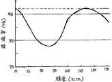
また、この厚みのITO膜は、その屈折率(550nmの波長で約2.0)から、透明導電膜付き基板の透過率は、図4に示すように厚みに大きく依存し、透過率を安定して得にくく、また透過率が透明導電膜が成膜されていない基板部分と大きく異なり、透明電極のある部分が容易に視認できてしまうという、商品上の不具合点を有する原因になっていた。 In addition, the ITO film with this thickness has a refractive index (approximately 2.0 at a wavelength of 550 nm), and the transmittance of the substrate with a transparent conductive film greatly depends on the thickness as shown in FIG. It was difficult to obtain, and the transmittance was greatly different from the substrate portion on which the transparent conductive film was not formed, which caused the product to have a defect in that the portion with the transparent electrode could be easily visually recognized. .
このような問題点を回避、克服するために、ITO膜の光学膜厚(屈折率nと実膜厚dの積nd)を可視光線領域の中央部分の波長である550nmの半波長(1/2)λ(λ=550nm)とし、つまり実膜厚としては138nm付近にすると、高透過率となることが知られている(図4参照)。しかしながら、ITO膜の表面抵抗が適切でないために、高い透過率が得られる膜厚が138nm付近では、抵抗値が低くなり、タッチパネルのON状態で流れる電流が大きくなり消費電力が増大してしまうという課題があった。 In order to avoid and overcome such problems, the optical film thickness (product nd of refractive index n and actual film thickness d) of the ITO film is set to a half wavelength (1 / 2) It is known that when λ (λ = 550 nm), that is, when the actual film thickness is around 138 nm, high transmittance is obtained (see FIG. 4). However, since the surface resistance of the ITO film is not appropriate, the resistance value is low when the film thickness at which high transmittance is obtained is around 138 nm, and the current flowing in the ON state of the touch panel increases, resulting in an increase in power consumption. There was a problem.
一方、最近、酸化亜鉛系の透明導電膜は、著しく性能改善が進み、ITO膜と同程度の透明性、電気特性が得られるようになってきた。このため、資源の枯渇のおそれがあり、また、高価なインジウム等を成分とするITO膜に代替し得る次世代の透明導電膜として、酸化亜鉛系透明導電膜に対する期待が高まっている。 On the other hand, recently, the performance of zinc oxide-based transparent conductive films has been remarkably improved, and transparency and electrical characteristics comparable to those of ITO films have been obtained. For this reason, there is a risk of depletion of resources, and expectation for a zinc oxide-based transparent conductive film is increasing as a next-generation transparent conductive film that can be replaced with an ITO film containing expensive indium or the like as a component.
酸化亜鉛系透明導電膜をタッチパネル用の透明電極に用いる場合は、酸化亜鉛の表面抵抗はITO膜に比較して大きいため、タッチパネルの透明電極に要求される中程度の表面抵抗を比較的簡単に得られるが、タッチパネルとして行う耐久性評価、具体的には、耐熱、耐湿熱環境試験での抵抗値安定性が悪く、タッチパネル用の透明電極として用いる場合に、上記耐久性の改善が望まれていた。 When using a zinc oxide-based transparent conductive film for a transparent electrode for a touch panel, the surface resistance of zinc oxide is larger than that of an ITO film. Although it is obtained, durability evaluation performed as a touch panel, specifically, resistance value stability in a heat and humidity heat resistance environment test is poor, and when used as a transparent electrode for a touch panel, improvement of the durability is desired. It was.
本発明は、タッチパネル用基板の透明導電膜として、資源枯渇問題のあるITO代替材料として、現在注目を集めている酸化亜鉛系透明導電膜を用い、上記の問題点を解決することを課題とする。すなわち
1)透過率が高いこと
2)耐久性があること
3)表面抵抗率がタッチパネルを得るのに好適な抵抗値を併せ有する透明導電膜付き基板を提供することを目的とする。An object of the present invention is to solve the above-mentioned problems by using a zinc oxide-based transparent conductive film which is currently attracting attention as an ITO alternative material having a resource depletion problem as a transparent conductive film for a touch panel substrate. . That is, the object is to provide a substrate with a transparent conductive film having 1) high transmittance, 2) durability, and 3) a surface resistivity that is suitable for obtaining a touch panel.
請求項1の発明は、主成分である酸化亜鉛に対し、ガリウムをGa2O3換算で1〜15重量パーセントの割合で含有することを特徴とする酸化亜鉛系透明導電膜である。The invention according to claim 1 is a zinc oxide-based transparent conductive film characterized by containing gallium in a proportion of 1 to 15 weight percent in terms of Ga2 O3 with respect to zinc oxide as a main component.
本発明の酸化亜鉛系透明導電膜のうち、ガリウムは膜の表面抵抗を制御する成分であり、また耐熱性、耐湿熱性などの耐久性を向上させる成分である。 Of the zinc oxide-based transparent conductive film of the present invention, gallium is a component that controls the surface resistance of the film, and is a component that improves durability such as heat resistance and moist heat resistance.
Ga2O3が1重量パーセント未満であると、膜の表面抵抗が大きくなるので好ましくない。また、樹脂フィルムとの張り合わせ工程などで加熱処理を受けると、抵抗が大きく上昇し、耐久性が悪くなるので好ましくない。一方Ga2O3が15重量パーセントを超えると、膜の表面抵抗が大きくなるだけでなく、ガリウムの増量によるコスト増を招くため好ましくない。When Ga2 O3 is less than 1 weight percent, the surface resistance of the film increases, which is not preferable. Moreover, when it heat-processes at the bonding process with a resin film etc., resistance will raise large and durability will worsen, and is unpreferable. On the other hand, when Ga2 O3 exceeds 15 weight percent, not only the surface resistance of the film increases, but also the cost increases due to an increase in the amount of gallium, which is not preferable.
請求項2の発明によれば、酸化亜鉛系透明導電膜の表面抵抗を200〜1000Ω/□とすることができる。透明導電膜の表面抵抗が200Ω/□未満であると、二枚の透明基板が対向配置されるようにしてタッチパネルを構成すると、対向する透明導電膜が接触(ON時)するときに流れる電流が大きくなり、消費電流が大きくなるので好ましくない。また透明導電膜の表面抵抗が1000Ω/□を越えると、接触時の電気的導通が不安定になるので好ましくない。 According to the invention of
請求項3の発明は、請求項1または2において、酸化亜鉛系透明導電膜の厚みが20〜400nmであり、全光線透過率が80%以上であることを特徴とする。 The invention of
本発明の酸化亜鉛系透明導電膜は、550nmの波長における屈折率が約2.0である酸化亜鉛を主成分として構成されている。したがって本発明の酸化亜鉛系透明導電膜は、550nmの波長における屈折率は、約2.0であることを特徴とする。 The zinc oxide-based transparent conductive film of the present invention is composed mainly of zinc oxide having a refractive index of about 2.0 at a wavelength of 550 nm. Therefore, the zinc oxide based transparent conductive film of the present invention has a refractive index of about 2.0 at a wavelength of 550 nm.
550nmにおける屈折率が約1.5であるガラスまたは樹脂の一方の表面に本発明の屈折率の透明導電膜が成膜されたときの両者を透過する全光線透過率は、図4に示されるように膜の厚みにより変化する。 When the transparent conductive film having the refractive index of the present invention is formed on one surface of glass or resin having a refractive index of about 1.5 at 550 nm, the total light transmittance which transmits both is shown in FIG. Thus, it varies depending on the thickness of the film.
請求項3の発明によれば、全光線透過率は80%以上と高いので、請求項5以下にあるように、それを用いたタッチパネル基板では、その表示が暗くなることがない。さらに視認性が良好で透過率の高いタッチパネルにする場合、酸化亜鉛系透明導電膜の厚みを120〜160nmにするとより好ましい。この透明導電膜の光学膜厚は設計波長λの大略半波長に相当する。酸化亜鉛膜の厚みを120〜160nmの範囲にすることにより、透明導電膜と基板とを透過する全光線透過率は、図4から明らかなように、基板のみの透過率(93%)により近づくため好ましい。 According to the invention of
請求項4の発明は、請求項1〜3の発明において、耐久性が熱処理(80℃、500時間)または、湿熱処理(60℃95%RH、500時間)を実施した前後の表面抵抗変化が0.8%以上1.3%以下であることを特徴とする。 According to a fourth aspect of the present invention, in the first to third aspects of the present invention, the change in surface resistance before and after the heat treatment (80 ° C., 500 hours) or wet heat treatment (60 ° C. 95% RH, 500 hours) is performed. It is characterized by being 0.8% or more and 1.3% or less.
請求項5〜8の発明は、請求項1〜4記載の酸化亜鉛系透明導電膜を透明基板上に成膜したことを特徴とするタッチパネル用基板である。すなわち、透過率が高く、耐久性が良好で、表面抵抗が省電力型のタッチパネルを得るのに好適な抵抗値を併せ有することにより、省電力でありかつON−OFFのスイッチング動作が、使用環境、使用時間に依存せず、確実に行えるタッチパネル用基板とすることが可能となる。 The invention according to
請求項9の発明は、透明基板をガラスもしく樹脂とすることを特徴とする。ガラスの材質としては、アルカリ成分の溶出がない無アルカリガラスが望ましい。樹脂の材質としては、水やトルエンなどのアウトガスが少なく、耐熱性が高い環状ポリオレフィン樹脂が望ましい。厚さは特に限定されるものではなく、透明基板自体の強度や用途に応じて適宜選択される。 The invention of
請求項10の発明は、請求項9のタッチパネル用基板を一方の基板に用いた抵抗膜方式タッチパネルである。この抵抗膜方式タッチパネルは、透明電極部分の透過率が高いので表示品質がよい。また、耐久性が良好であるため、屋内外での長期使用が可能である。さらに、透明電極の表面抵抗が所定の値に制御されることにより、省電力であり、かつスイッチング動作が確実に行える。 A tenth aspect of the present invention is a resistive touch panel using the touch panel substrate of the ninth aspect as one substrate. This resistive film type touch panel has a high display quality because the transmittance of the transparent electrode portion is high. Moreover, since durability is favorable, long-term use indoors and outdoors is possible. Furthermore, by controlling the surface resistance of the transparent electrode to a predetermined value, it is possible to save power and to perform a switching operation with certainty.
本発明のタッチパネル用基板は、透明基板に、酸化亜鉛を主成分とし、ガリウムを所定の範囲で含有した酸化亜鉛系透明導電膜を所定の膜厚にて成膜することにより、高い透過率を得ることができ、屋内外での長期使用が可能で、表面抵抗をタッチパネルに好適な中程度の抵抗値にすることができる。これにより、コスト高で資源枯渇問題のあるITO膜の代替が可能な、酸化亜鉛系透明導電膜を用いた抵抗膜方式タッチパネルを得ることができる。 The touch panel substrate of the present invention has a high transmittance by forming a zinc oxide-based transparent conductive film containing zinc oxide as a main component and containing gallium in a predetermined range on a transparent substrate in a predetermined film thickness. It can be obtained, can be used indoors and outdoors for a long time, and the surface resistance can be set to a moderate resistance value suitable for a touch panel. Thereby, it is possible to obtain a resistive film type touch panel using a zinc oxide-based transparent conductive film, which can be replaced with an ITO film which is costly and has a problem of resource depletion.
図1は、本発明のタッチパネル用基板の一実施例の断面図である。タッチパネル用基板1は、透明基板3の一方の表面に酸化亜鉛系透明導電膜2が成膜されている。透明基板は、ガラスや樹脂を用いることができる。ガラスは無アルカリガラス、石英ガラス、ホウケイ酸ガラスなどとくに組成が限定されない。ガラス中にソーダ成分を多量に含む場合は、二酸化珪素などのアルカリ溶出防止膜を設けてもよい。樹脂は環状ポリオレフィン、ポリカーボネート、ポリエーテルスルホン、ポリエチレンテレフタレート、ポリエチレンナフタレートなどの樹脂を例示することができる。樹脂からのアウトガス成分を防止するために、珪素の酸化物、窒化物等のアンダーコート層を設けてもよい。 FIG. 1 is a cross-sectional view of an embodiment of a touch panel substrate of the present invention. In the touch panel substrate 1, a zinc oxide-based transparent
本発明の透明導電膜は、イオンプレーティング法、スパッタリング法、真空蒸着法などの公知の方法で基板表面に成膜することができる。なかでも、イオンプレーティング法は基板を高温に加熱する必要がなく、樹脂にも成膜することができる点で好ましい。 The transparent conductive film of the present invention can be formed on the substrate surface by a known method such as an ion plating method, a sputtering method, or a vacuum evaporation method. Among these, the ion plating method is preferable in that it is not necessary to heat the substrate to a high temperature and the film can be formed on a resin.
イオンプレーティング法は、成膜室に配設した電極部としてのハース等に、成膜材料として、ガリウムを含有する酸化亜鉛の微粉末を焼結したターゲットを配置し、このターゲットに例えばアルゴンプラズマを照射してターゲットを加熱し、蒸発させ、プラズマを通過した酸化亜鉛等の各粒子をハース等に対向する位置に置かれた基板に成膜する方法である。 In the ion plating method, a target obtained by sintering a fine powder of zinc oxide containing gallium as a film forming material is disposed on a hearth as an electrode portion disposed in a film forming chamber, and an argon plasma, for example, is disposed on this target. , The target is heated and evaporated, and each particle such as zinc oxide that has passed through the plasma is deposited on a substrate placed at a position facing the hearth or the like.
イオンプレーティング法は、例えばスパッタ法に比べ、粒子の持つ運動エネルギーが小さいため、粒子が衝突するときに基板や基板に成膜させた酸化亜鉛膜に与えるダメージが小さく、結晶性の良好な膜を得ることができる。 Films with good crystallinity, such as ion plating, have less kinetic energy of particles than, for example, sputtering, and therefore less damage to the substrate and the zinc oxide film deposited on the substrate when the particles collide. Can be obtained.
図2は、本発明により得られるタッチパネル用基板1と樹脂板5が本発明にかかる酸化亜鉛系透明導電膜2と透明導電膜4とが対向するように配置し、樹脂板5と本発明のタッチパネル用基板1の間をドットスペーサ6により約1mmの間隔で固定した。 FIG. 2 shows that the touch panel substrate 1 and the
図3は、本発明のタッチパネルの動作状態を説明する図で、矢印の方向に指で押圧することにより樹脂板5が変形し、樹脂板5に形成された透明導電膜(透明電極)4と透明基板3に形成された透明導電膜(透明電極)2が接触してON状態になり、両電極間に電流が流れる。指を樹脂板5から離すことにより、樹脂板5の形状は初期の位置に戻り、OFF状態になる。本発明のタッチパネルは、透明電極2を、酸化亜鉛にガリウムを含有した、酸化亜鉛系透明導電膜とし、表面抵抗を200〜1000Ω/□とすることにより、ON状態の電流を小さくすることができ、かつON時の電気的接触を確実にすることができた。また、この抵抗範囲を確保しながら、透過率を高くすることができるので表示の品位がよい。さらに、耐熱、耐湿熱環境試験での抵抗値安定性、つまり耐久性が良好であるため屋内外での長期使用が可能である。 FIG. 3 is a diagram for explaining the operating state of the touch panel of the present invention. When the
以下に、実施例および比較例を用いて本発明を詳述する。用いた透明基板は、厚み0.7mmの無アルカリガラスを用いた。透明導電膜の成膜はイオンプレーティング法により行った。成膜条件を下記に示す。
1)成膜前の基板の予備加熱:なし
2)成膜時の圧力:0.1Pa
3)雰囲気ガス条件:アルゴン=100sccm、酸素=40sccm
4)ターゲット:表1に示す割合で、ガリウムを含有している酸化亜鉛焼結体The present invention will be described in detail below using examples and comparative examples. The transparent substrate used was non-alkali glass having a thickness of 0.7 mm. The transparent conductive film was formed by an ion plating method. The film forming conditions are shown below.
1) Preheating of substrate before film formation: None 2) Pressure during film formation: 0.1 Pa
3) Atmospheric gas conditions: argon = 100 sccm, oxygen = 40 sccm
4) Target: Zinc oxide sintered body containing gallium in the ratio shown in Table 1
実施例中の物性値は次の方法により測定した。
<表面抵抗>
表面抵抗は、JIS K 7194に準拠し、三菱化学株式会社製 ロレスタEPにて測定した。
<全光線透過率>
全光線透過率は、ASTM D 1003に準拠し、株式会社村上色彩技術研究所製 HM−100型にて測定した。
<耐熱性>
熱処理として、80℃にセットした熱風オーブン装置で500時間処理する前後の表面抵抗変化(R/R0)を測定した。
<耐湿熱性>
湿熱処理として、60℃95%RHにセットした恒温恒湿槽で500時間処理する前後の表面抵抗変化(R/R0)を測定した。The physical property values in the examples were measured by the following methods.
<Surface resistance>
The surface resistance was measured with Loresta EP manufactured by Mitsubishi Chemical Corporation in accordance with JIS K 7194.
<Total light transmittance>
The total light transmittance was measured by Murakami Color Research Laboratory Co., Ltd. HM-100 type according to ASTM D 1003.
<Heat resistance>
As the heat treatment, the change in surface resistance (R / R0) before and after treatment for 500 hours in a hot air oven set at 80 ° C. was measured.
<Heat and heat resistance>
As the wet heat treatment, the change in surface resistance (R / R0) before and after treatment for 500 hours in a constant temperature and humidity chamber set at 60 ° C. and 95% RH was measured.
(実施例1〜5、比較例1〜2)
酸化亜鉛に対し、ガリウムをGa2O3換算で表1に記載の割合で含有している酸化亜鉛焼結体をターゲットとした。この焼結体ターゲットを用いて、イオンプレーティング法によりガラス基板上に、表1に記載の膜厚になるように成膜した。その結果を表1に示す。
The target was a zinc oxide sintered body containing gallium in a ratio shown in Table 1 in terms of Ga2 O3 with respect to zinc oxide. Using this sintered compact target, it formed into a film so that it might become the film thickness of Table 1 on the glass substrate by the ion plating method. The results are shown in Table 1.
1:本発明のタッチパネル用基板
2:酸化亜鉛系透明導電膜
3:透明基板(ガラスもしくは樹脂)
4:透明導電膜
5:樹脂
6:ドットスペーサ
7:本発明のタッチパネル1: Touch panel substrate of the present invention 2: Zinc oxide-based transparent conductive film 3: Transparent substrate (glass or resin)
4: Transparent conductive film 5: Resin 6: Dot spacer 7: Touch panel of the present invention
Claims (10)
Translated fromJapanesePriority Applications (1)
| Application Number | Priority Date | Filing Date | Title |
|---|---|---|---|
| JP2005295891AJP2007109406A (en) | 2005-10-11 | 2005-10-11 | Substrate with zinc oxide transparent conductive film for touch panel |
Applications Claiming Priority (1)
| Application Number | Priority Date | Filing Date | Title |
|---|---|---|---|
| JP2005295891AJP2007109406A (en) | 2005-10-11 | 2005-10-11 | Substrate with zinc oxide transparent conductive film for touch panel |
Publications (1)
| Publication Number | Publication Date |
|---|---|
| JP2007109406Atrue JP2007109406A (en) | 2007-04-26 |
Family
ID=38035131
Family Applications (1)
| Application Number | Title | Priority Date | Filing Date |
|---|---|---|---|
| JP2005295891APendingJP2007109406A (en) | 2005-10-11 | 2005-10-11 | Substrate with zinc oxide transparent conductive film for touch panel |
Country Status (1)
| Country | Link |
|---|---|
| JP (1) | JP2007109406A (en) |
Cited By (8)
| Publication number | Priority date | Publication date | Assignee | Title |
|---|---|---|---|---|
| JP2009114538A (en)* | 2007-10-19 | 2009-05-28 | Hakusui Tech Co Ltd | Ion plating target for zinc oxide thin film production |
| JP2010009096A (en)* | 2008-06-24 | 2010-01-14 | Epson Imaging Devices Corp | Input device and display with input function |
| DE112008004011T5 (en) | 2008-09-24 | 2011-07-14 | Toshiba Mitsubishi-Electric Industrial Systems Corporation | A method of forming zinc oxide film (ZnO) or magnesium zinc oxide film (ZnMgO) and zinc oxide film or magnesium zinc oxide film forming apparatus |
| CN102191455A (en)* | 2010-03-15 | 2011-09-21 | 三菱综合材料株式会社 | Vapour deposition material for forming film, film sheet and laminated sheet having the same |
| DE112008004012T5 (en) | 2008-09-24 | 2011-09-29 | Toshiba Mitsubishi-Electric Industrial Systems Corporation | Process for producing a metal oxide film and apparatus for producing a metal oxide film |
| JP2011214136A (en)* | 2010-03-15 | 2011-10-27 | Mitsubishi Materials Corp | Vapor deposition material for forming thin film, thin film sheet having the thin film, and laminated sheet |
| KR101089873B1 (en)* | 2009-10-01 | 2011-12-05 | 삼성전기주식회사 | Input device of touch screen and manufacturing method thereof |
| DE112010005624T5 (en) | 2010-06-01 | 2013-03-21 | Kyoto University | A metal oxide film forming apparatus, a metal oxide film forming method and a metal oxide film |
Citations (4)
| Publication number | Priority date | Publication date | Assignee | Title |
|---|---|---|---|---|
| JPH02181304A (en)* | 1988-09-22 | 1990-07-16 | Nippon Soken Inc | Zinc oxide transparent conductive film and manufacture thereof |
| JPH07249316A (en)* | 1994-03-10 | 1995-09-26 | Asahi Glass Co Ltd | Transparent conductive film and transparent substrate using the transparent conductive film |
| JPH0853761A (en)* | 1993-07-28 | 1996-02-27 | Asahi Glass Co Ltd | Method for producing transparent conductive film |
| JP2004095223A (en)* | 2002-08-29 | 2004-03-25 | Sumitomo Heavy Ind Ltd | Method for producing zinc oxide-based transparent conductive film |
- 2005
- 2005-10-11JPJP2005295891Apatent/JP2007109406A/enactivePending
Patent Citations (4)
| Publication number | Priority date | Publication date | Assignee | Title |
|---|---|---|---|---|
| JPH02181304A (en)* | 1988-09-22 | 1990-07-16 | Nippon Soken Inc | Zinc oxide transparent conductive film and manufacture thereof |
| JPH0853761A (en)* | 1993-07-28 | 1996-02-27 | Asahi Glass Co Ltd | Method for producing transparent conductive film |
| JPH07249316A (en)* | 1994-03-10 | 1995-09-26 | Asahi Glass Co Ltd | Transparent conductive film and transparent substrate using the transparent conductive film |
| JP2004095223A (en)* | 2002-08-29 | 2004-03-25 | Sumitomo Heavy Ind Ltd | Method for producing zinc oxide-based transparent conductive film |
Cited By (10)
| Publication number | Priority date | Publication date | Assignee | Title |
|---|---|---|---|---|
| JP2009114538A (en)* | 2007-10-19 | 2009-05-28 | Hakusui Tech Co Ltd | Ion plating target for zinc oxide thin film production |
| JP2010009096A (en)* | 2008-06-24 | 2010-01-14 | Epson Imaging Devices Corp | Input device and display with input function |
| DE112008004011T5 (en) | 2008-09-24 | 2011-07-14 | Toshiba Mitsubishi-Electric Industrial Systems Corporation | A method of forming zinc oxide film (ZnO) or magnesium zinc oxide film (ZnMgO) and zinc oxide film or magnesium zinc oxide film forming apparatus |
| DE112008004012T5 (en) | 2008-09-24 | 2011-09-29 | Toshiba Mitsubishi-Electric Industrial Systems Corporation | Process for producing a metal oxide film and apparatus for producing a metal oxide film |
| US9598768B2 (en) | 2008-09-24 | 2017-03-21 | Toshiba Mitsubishi-Electric Industrial Systems Corporation | Method of forming zinc oxide film (ZnO) or magnesium zinc oxide film (ZnMgO) and apparatus for forming zinc oxide film or magnesium zinc oxide film |
| KR101089873B1 (en)* | 2009-10-01 | 2011-12-05 | 삼성전기주식회사 | Input device of touch screen and manufacturing method thereof |
| CN102191455A (en)* | 2010-03-15 | 2011-09-21 | 三菱综合材料株式会社 | Vapour deposition material for forming film, film sheet and laminated sheet having the same |
| JP2011214136A (en)* | 2010-03-15 | 2011-10-27 | Mitsubishi Materials Corp | Vapor deposition material for forming thin film, thin film sheet having the thin film, and laminated sheet |
| DE112010005624T5 (en) | 2010-06-01 | 2013-03-21 | Kyoto University | A metal oxide film forming apparatus, a metal oxide film forming method and a metal oxide film |
| US9279182B2 (en) | 2010-06-01 | 2016-03-08 | Toshiba Mitsubishi-Electric Industrial Systems Corporation | Apparatus for forming metal oxide film, method for forming metal oxide film, and metal oxide film |
Similar Documents
| Publication | Publication Date | Title |
|---|---|---|
| KR100696905B1 (en) | Substrate for a contact panel having a transparent conductive film and a resistive film type transparent contact panel including the same | |
| KR101007170B1 (en) | Crystalline transparent conductive thin film, its manufacturing method, transparent conductive film, and touch panel | |
| CN101622714B (en) | Thin film transistor and manufacturing method thereof | |
| EP1720175B1 (en) | Transparent conductive film and transparent conductive base material utilizing the same | |
| KR100821541B1 (en) | Transparent conductive film | |
| KR100788775B1 (en) | Transparent electroconductive film and touch panel | |
| US6146765A (en) | Transparent conductive film and method for its production, and sputtering target | |
| JP2012509397A (en) | Method for manufacturing ITO coated product for use with touch panel display and / or method for manufacturing said ITO coated product | |
| KR20160035998A (en) | Conductive structure body and method for manufacturing the same | |
| JP5962663B2 (en) | Glass plate with transparent conductive film | |
| CN102324271A (en) | Crystallized type ITO (Indium Tin Oxide) transparent conductive film and preparation method thereof | |
| JP4067141B2 (en) | Transparent conductive film, method for producing the same, and sputtering target | |
| JP2007109406A (en) | Substrate with zinc oxide transparent conductive film for touch panel | |
| CN111902561B (en) | Shield layer, method for producing shield layer, and oxide sputtering target | |
| JP4687733B2 (en) | Transparent electrode, transparent conductive substrate and transparent touch panel | |
| JP2018518787A (en) | Touch-controlled display device having a high resistivity layer | |
| TWI882248B (en) | Molybdenum oxide based sintered body, sputtering target, oxide thin film using the sintered body, and thin film transistors and display devices including the thin films | |
| JP2019194352A (en) | Shield layer and manufacturing method of shield layer and oxide sputtering target | |
| JP4358251B2 (en) | Method for forming high resistance tin-doped indium oxide film | |
| CN115925414B (en) | Molybdenum oxide-based sintered body, thin film using the sintered body, thin film transistor including the thin film, and display device | |
| JP2003335547A (en) | Glass substrate for flat panel display equipment | |
| CN106024110A (en) | Strontium stannate-based flexible transparent conductive electrode and preparation method thereof | |
| JP2007277016A (en) | Lead-free glass for flat fluorescent lamp electrode coating | |
| JP2002073280A (en) | Substrate for transparent touch panel and transparent touch panel | |
| JP2004035295A (en) | Glass substrate for flat panel display device |
Legal Events
| Date | Code | Title | Description |
|---|---|---|---|
| A711 | Notification of change in applicant | Free format text:JAPANESE INTERMEDIATE CODE: A712 Effective date:20070809 | |
| RD02 | Notification of acceptance of power of attorney | Free format text:JAPANESE INTERMEDIATE CODE: A7422 Effective date:20080414 | |
| A521 | Written amendment | Free format text:JAPANESE INTERMEDIATE CODE: A821 Effective date:20080414 | |
| A621 | Written request for application examination | Free format text:JAPANESE INTERMEDIATE CODE: A621 Effective date:20080930 | |
| A711 | Notification of change in applicant | Free format text:JAPANESE INTERMEDIATE CODE: A711 Effective date:20090528 | |
| A977 | Report on retrieval | Free format text:JAPANESE INTERMEDIATE CODE: A971007 Effective date:20110117 | |
| A131 | Notification of reasons for refusal | Free format text:JAPANESE INTERMEDIATE CODE: A131 Effective date:20110208 | |
| A02 | Decision of refusal | Free format text:JAPANESE INTERMEDIATE CODE: A02 Effective date:20110726 |