JP2007109216A - Semiconductor device - Google Patents
Semiconductor deviceDownload PDFInfo
- Publication number
- JP2007109216A JP2007109216AJP2006241019AJP2006241019AJP2007109216AJP 2007109216 AJP2007109216 AJP 2007109216AJP 2006241019 AJP2006241019 AJP 2006241019AJP 2006241019 AJP2006241019 AJP 2006241019AJP 2007109216 AJP2007109216 AJP 2007109216A
- Authority
- JP
- Japan
- Prior art keywords
- antenna
- semiconductor device
- integrated circuit
- circuit
- integrated circuits
- Prior art date
- Legal status (The legal status is an assumption and is not a legal conclusion. Google has not performed a legal analysis and makes no representation as to the accuracy of the status listed.)
- Withdrawn
Links
- 239000004065semiconductorSubstances0.000titleclaimsabstractdescription126
- 239000000758substrateSubstances0.000claimsabstractdescription68
- 238000004891communicationMethods0.000claimsabstractdescription30
- 238000003860storageMethods0.000claimsdescription5
- 238000000034methodMethods0.000abstractdescription35
- 230000008569processEffects0.000abstractdescription7
- 239000010410layerSubstances0.000description55
- 239000011241protective layerSubstances0.000description23
- 239000012298atmosphereSubstances0.000description16
- VYPSYNLAJGMNEJ-UHFFFAOYSA-Nsilicon dioxideInorganic materialsO=[Si]=OVYPSYNLAJGMNEJ-UHFFFAOYSA-N0.000description16
- 239000012535impuritySubstances0.000description13
- 239000007789gasSubstances0.000description12
- 230000006870functionEffects0.000description10
- 229910052581Si3N4Inorganic materials0.000description9
- 229920005989resinPolymers0.000description9
- 239000011347resinSubstances0.000description9
- HQVNEWCFYHHQES-UHFFFAOYSA-Nsilicon nitrideChemical compoundN12[Si]34N5[Si]62N3[Si]51N64HQVNEWCFYHHQES-UHFFFAOYSA-N0.000description9
- IJGRMHOSHXDMSA-UHFFFAOYSA-NAtomic nitrogenChemical compoundN#NIJGRMHOSHXDMSA-UHFFFAOYSA-N0.000description8
- UFHFLCQGNIYNRP-UHFFFAOYSA-NHydrogenChemical compound[H][H]UFHFLCQGNIYNRP-UHFFFAOYSA-N0.000description8
- XUIMIQQOPSSXEZ-UHFFFAOYSA-NSiliconChemical compound[Si]XUIMIQQOPSSXEZ-UHFFFAOYSA-N0.000description8
- 239000003814drugSubstances0.000description8
- 239000001257hydrogenSubstances0.000description8
- 229910052739hydrogenInorganic materials0.000description8
- 239000000463materialSubstances0.000description8
- 229910052710siliconInorganic materials0.000description8
- 239000010703siliconSubstances0.000description8
- 239000002585baseSubstances0.000description7
- QGZKDVFQNNGYKY-UHFFFAOYSA-NAmmoniaChemical compoundNQGZKDVFQNNGYKY-UHFFFAOYSA-N0.000description6
- 206010020751HypersensitivityDiseases0.000description6
- 230000006378damageEffects0.000description6
- 239000011521glassSubstances0.000description6
- 238000005121nitridingMethods0.000description6
- 238000012545processingMethods0.000description6
- 235000012239silicon dioxideNutrition0.000description6
- 229910052814silicon oxideInorganic materials0.000description6
- 238000002425crystallisationMethods0.000description5
- 238000004519manufacturing processMethods0.000description5
- 239000002245particleSubstances0.000description5
- 238000009832plasma treatmentMethods0.000description5
- 239000002356single layerSubstances0.000description5
- GQPLMRYTRLFLPF-UHFFFAOYSA-NNitrous OxideChemical compound[O-][N+]#NGQPLMRYTRLFLPF-UHFFFAOYSA-N0.000description4
- QVGXLLKOCUKJST-UHFFFAOYSA-Natomic oxygenChemical compound[O]QVGXLLKOCUKJST-UHFFFAOYSA-N0.000description4
- 230000015572biosynthetic processEffects0.000description4
- 229910052802copperInorganic materials0.000description4
- 239000013078crystalSubstances0.000description4
- 229910052757nitrogenInorganic materials0.000description4
- 230000001590oxidative effectEffects0.000description4
- 239000001301oxygenSubstances0.000description4
- 229910052760oxygenInorganic materials0.000description4
- 239000010453quartzSubstances0.000description4
- OKTJSMMVPCPJKN-UHFFFAOYSA-NCarbonChemical compound[C]OKTJSMMVPCPJKN-UHFFFAOYSA-N0.000description3
- 239000000853adhesiveSubstances0.000description3
- 230000001070adhesive effectEffects0.000description3
- 208000026935allergic diseaseDiseases0.000description3
- 208000030961allergic reactionDiseases0.000description3
- 230000007815allergyEffects0.000description3
- 229910021529ammoniaInorganic materials0.000description3
- 238000005452bendingMethods0.000description3
- 230000008901benefitEffects0.000description3
- 229910052799carbonInorganic materials0.000description3
- 238000005530etchingMethods0.000description3
- 238000005984hydrogenation reactionMethods0.000description3
- 238000007689inspectionMethods0.000description3
- 230000004044responseEffects0.000description3
- 239000000377silicon dioxideSubstances0.000description3
- 125000001424substituent groupChemical group0.000description3
- 229910045601alloyInorganic materials0.000description2
- 239000000956alloySubstances0.000description2
- 229910052782aluminiumInorganic materials0.000description2
- 229910021417amorphous siliconInorganic materials0.000description2
- 229910052786argonInorganic materials0.000description2
- 230000004888barrier functionEffects0.000description2
- WPYMKLBDIGXBTP-UHFFFAOYSA-Nbenzoic acidChemical compoundOC(=O)C1=CC=CC=C1WPYMKLBDIGXBTP-UHFFFAOYSA-N0.000description2
- 230000000903blocking effectEffects0.000description2
- 239000000919ceramicSubstances0.000description2
- 239000011248coating agentSubstances0.000description2
- 238000000576coating methodMethods0.000description2
- 230000008025crystallizationEffects0.000description2
- 238000009826distributionMethods0.000description2
- 229940079593drugDrugs0.000description2
- 238000005516engineering processMethods0.000description2
- 125000001153fluoro groupChemical groupF*0.000description2
- 235000013305foodNutrition0.000description2
- 230000007274generation of a signal involved in cell-cell signalingEffects0.000description2
- 229910052737goldInorganic materials0.000description2
- 229910052734heliumInorganic materials0.000description2
- 150000002431hydrogenChemical class0.000description2
- 230000010365information processingEffects0.000description2
- 150000002500ionsChemical class0.000description2
- 229910052743kryptonInorganic materials0.000description2
- 230000007257malfunctionEffects0.000description2
- 229910052751metalInorganic materials0.000description2
- 239000002184metalSubstances0.000description2
- 229910044991metal oxideInorganic materials0.000description2
- 150000004706metal oxidesChemical class0.000description2
- 229910052750molybdenumInorganic materials0.000description2
- 229910052754neonInorganic materials0.000description2
- 150000004767nitridesChemical class0.000description2
- 229960001730nitrous oxideDrugs0.000description2
- 235000013842nitrous oxideNutrition0.000description2
- 125000000962organic groupChemical group0.000description2
- 238000004806packaging method and processMethods0.000description2
- 239000004033plasticSubstances0.000description2
- 238000005498polishingMethods0.000description2
- 230000001681protective effectEffects0.000description2
- 239000002994raw materialSubstances0.000description2
- 229910052709silverInorganic materials0.000description2
- 239000004094surface-active agentSubstances0.000description2
- 229910052715tantalumInorganic materials0.000description2
- 229910052719titaniumInorganic materials0.000description2
- 229910052721tungstenInorganic materials0.000description2
- 229910052724xenonInorganic materials0.000description2
- 239000005711Benzoic acidSubstances0.000description1
- 241001465754MetazoaSpecies0.000description1
- 229910052779NeodymiumInorganic materials0.000description1
- 239000004952PolyamideSubstances0.000description1
- 239000004695Polyether sulfoneSubstances0.000description1
- 239000004642PolyimideSubstances0.000description1
- NIXOWILDQLNWCW-UHFFFAOYSA-Nacrylic acid groupChemical groupC(C=C)(=O)ONIXOWILDQLNWCW-UHFFFAOYSA-N0.000description1
- 239000000654additiveSubstances0.000description1
- 230000000996additive effectEffects0.000description1
- 230000002411adverseEffects0.000description1
- 229910052783alkali metalInorganic materials0.000description1
- 150000001340alkali metalsChemical class0.000description1
- 229910052784alkaline earth metalInorganic materials0.000description1
- 150000001342alkaline earth metalsChemical class0.000description1
- 125000000217alkyl groupChemical group0.000description1
- 239000005407aluminoborosilicate glassSubstances0.000description1
- 238000000137annealingMethods0.000description1
- 150000004945aromatic hydrocarbonsChemical class0.000description1
- 229910052788bariumInorganic materials0.000description1
- DSAJWYNOEDNPEQ-UHFFFAOYSA-Nbarium atomChemical compound[Ba]DSAJWYNOEDNPEQ-UHFFFAOYSA-N0.000description1
- 235000010233benzoic acidNutrition0.000description1
- 239000005388borosilicate glassSubstances0.000description1
- 239000003795chemical substances by applicationSubstances0.000description1
- 238000005229chemical vapour depositionMethods0.000description1
- 229910052804chromiumInorganic materials0.000description1
- 150000001875compoundsChemical class0.000description1
- 239000004020conductorSubstances0.000description1
- 238000011109contaminationMethods0.000description1
- CFBGXYDUODCMNS-UHFFFAOYSA-NcyclobuteneChemical compoundC1CC=C1CFBGXYDUODCMNS-UHFFFAOYSA-N0.000description1
- 230000007547defectEffects0.000description1
- 230000006866deteriorationEffects0.000description1
- 238000011161developmentMethods0.000description1
- 238000010586diagramMethods0.000description1
- 238000009792diffusion processMethods0.000description1
- 238000007599dischargingMethods0.000description1
- 230000009977dual effectEffects0.000description1
- 238000005401electroluminescenceMethods0.000description1
- 239000003822epoxy resinSubstances0.000description1
- 230000002349favourable effectEffects0.000description1
- 239000010408filmSubstances0.000description1
- 238000010438heat treatmentMethods0.000description1
- 230000006872improvementEffects0.000description1
- 239000004615ingredientSubstances0.000description1
- 238000007641inkjet printingMethods0.000description1
- 230000001788irregularEffects0.000description1
- 238000004898kneadingMethods0.000description1
- 238000005499laser crystallizationMethods0.000description1
- 239000004973liquid crystal related substanceSubstances0.000description1
- 244000144972livestockSpecies0.000description1
- 229910052748manganeseInorganic materials0.000description1
- 238000002156mixingMethods0.000description1
- 239000000203mixtureSubstances0.000description1
- 229910021421monocrystalline siliconInorganic materials0.000description1
- 239000002105nanoparticleSubstances0.000description1
- 229910052759nickelInorganic materials0.000description1
- 229910052756noble gasInorganic materials0.000description1
- 230000003647oxidationEffects0.000description1
- 238000007254oxidation reactionMethods0.000description1
- 238000005268plasma chemical vapour depositionMethods0.000description1
- 229910052697platinumInorganic materials0.000description1
- 229920002647polyamidePolymers0.000description1
- 229920001230polyarylatePolymers0.000description1
- 239000004417polycarbonateSubstances0.000description1
- 229920000515polycarbonatePolymers0.000description1
- 229920000647polyepoxidePolymers0.000description1
- 229920006393polyether sulfonePolymers0.000description1
- 229920001721polyimidePolymers0.000description1
- 239000000843powderSubstances0.000description1
- 238000007639printingMethods0.000description1
- 230000003252repetitive effectEffects0.000description1
- 238000011160researchMethods0.000description1
- 238000007650screen-printingMethods0.000description1
- 239000007787solidSubstances0.000description1
- 229920003002synthetic resinPolymers0.000description1
- 239000000057synthetic resinSubstances0.000description1
- 238000009210therapy by ultrasoundMethods0.000description1
- 238000004804windingMethods0.000description1
Images


Landscapes
- Hardware Redundancy (AREA)
Abstract
Description
Translated fromJapanese本発明は、非接触で情報の入出力が可能(無線通信で情報の入出力が可能)な半導体装置に関する。 The present invention relates to a semiconductor device in which information can be input / output without contact (information can be input / output by wireless communication).
電波又は電磁波を利用して非接触で情報の読み出しと書き込みを行う認証システム(Radio Frequency Identification System、「RFIDシステム」、「RFID」ともいう)は、産業界においてバーコードに代わる識別・認証技術として研究が進められている。近年では、このような用途に限定されず、スーパーマーケットにおける商品管理や、航空旅客の預入手荷物管理など、新たなサービスの提供が展開されつつある。 An authentication system (Radio Frequency Identification System, also referred to as “RFID system” or “RFID”) that reads and writes information in a non-contact manner using radio waves or electromagnetic waves is an identification / authentication technology that replaces barcodes in the industry. Research is ongoing. In recent years, the present invention is not limited to such applications, and new services such as merchandise management in supermarkets and baggage management for air passengers are being developed.
RFID技術で用いる無線IC(無線通信可能な集積回路)は、アンテナを含めると数十ミリメートルの大きさで、無線通信によりリーダライタ機器と情報の送受信を行う。その形状は、ラベル型、タグ型、カード型、コイン型、スティック型など様々なものがある。 A wireless IC (integrated circuit capable of wireless communication) used in the RFID technology has a size of several tens of millimeters including an antenna, and transmits and receives information to and from a reader / writer device by wireless communication. There are various shapes such as a label type, a tag type, a card type, a coin type, and a stick type.
このような無線ICは、これまでに培ったシリコンウエハーに集積回路を形成する微細化技術を利用して製造されている。RFIDを普及させるには、そのコアデバイスとなる無線ICのコストを下げる必要があり、そのためにチップサイズの縮小化が進められている。さらに、シリコンウエハーを分断して微小な半導体チップを実装する方法の開発が進められている(例えば、特許文献1参照)。
しかしながら、アンテナとICチップを組み合わせた従来の無線ICは、広く普及させるために、小型化や低コスト化の努力がされていた。そして、従来の無線ICには一つのICチップしか配設されていないので、情報を記憶する容量が小さく、高機能化や多機能化に障害があった。 However, efforts have been made to reduce the size and cost of a conventional wireless IC that combines an antenna and an IC chip in order to widely spread. Since a conventional wireless IC is provided with only one IC chip, the capacity for storing information is small, and there are obstacles to high functionality and multi-function.
本発明は、このような状況に鑑み、多くの情報を処理することができ、多機能化にも対応することができる非接触で情報処理が可能な半導体装置の提供を目的とする。また、非接触で情報処理が可能な半導体装置の信頼性を向上させることを目的とする。 In view of such circumstances, an object of the present invention is to provide a semiconductor device capable of processing a large amount of information and capable of dealing with multi-function and capable of non-contact information processing. It is another object of the present invention to improve the reliability of a semiconductor device capable of non-contact information processing.
本発明は、入出力手段としてアンテナを共有する複数の集積回路を備えた半導体装置である。ICは無線通信可能な集積回路であって、集積回路には、通信回路と論理回路と記憶回路とを含ませることができる。通信回路には、高周波回路と変調回路と復調回路を含ませることもできる。記憶回路は、不揮発性メモリと読み出し専用メモリを含ませることもできる。この複数の集積回路は、通信周波数を同じものとすることができる。また、この複数の集積回路は、通信周波数を同じものとし、通信プロトコルを異ならせたものであっても良い。 The present invention is a semiconductor device including a plurality of integrated circuits sharing an antenna as input / output means. The IC is an integrated circuit capable of wireless communication, and the integrated circuit can include a communication circuit, a logic circuit, and a memory circuit. The communication circuit may include a high frequency circuit, a modulation circuit, and a demodulation circuit. The memory circuit can include a nonvolatile memory and a read-only memory. The plurality of integrated circuits can have the same communication frequency. The plurality of integrated circuits may have the same communication frequency and different communication protocols.
本発明の一は、アンテナと、当該アンテナに接続された複数の集積回路を有し、複数の集積回路は、それぞれ、識別符号と集積回路の動作を制御するプログラムが記憶された記憶回路を有し、識別符号は複数の集積回路のぞれぞれで異なり、プログラムは複数の集積回路のそれぞれで異なることを特徴とする半導体装置である。 One embodiment of the present invention includes an antenna and a plurality of integrated circuits connected to the antenna, and each of the plurality of integrated circuits includes a storage circuit in which an identification code and a program for controlling the operation of the integrated circuit are stored. The semiconductor device is characterized in that the identification code is different for each of the plurality of integrated circuits, and the program is different for each of the plurality of integrated circuits.
本発明の一は、アンテナと、当該アンテナに接続された複数の集積回路を有し、複数の集積回路は、それぞれ、識別符号と集積回路の動作を制御するプログラムが記憶された記憶回路を有し、複数の集積回路から選択された少なくとも2つの集積回路は、同じ識別符号と同じプログラムを有することを特徴とする半導体装置である。 One embodiment of the present invention includes an antenna and a plurality of integrated circuits connected to the antenna, and each of the plurality of integrated circuits includes a storage circuit in which an identification code and a program for controlling the operation of the integrated circuit are stored. At least two integrated circuits selected from the plurality of integrated circuits are semiconductor devices having the same identification code and the same program.
本発明の一は、アンテナと、アンテナに接続された複数の集積回路と、集積回路に接続された多数決回路を有し、複数の集積回路は、それぞれ、識別符号と集積回路の動作を制御するプログラムが記憶された記憶回路を有し、複数の集積回路から選択された少なくとも2つの集積回路は、同じ識別符号と同じプログラムを有し、多数決回路は、当該集積回路の通信に応じた複数の識別符号より、識別符号の多数決値である識別符号を出力し、アンテナは、多数決値である識別符号を基に変調された搬送波を出力することを特徴とする半導体装置である。 One embodiment of the present invention includes an antenna, a plurality of integrated circuits connected to the antenna, and a majority circuit connected to the integrated circuit, and the plurality of integrated circuits control the identification code and the operation of the integrated circuit, respectively. A memory circuit storing a program, at least two integrated circuits selected from the plurality of integrated circuits have the same program with the same identification code, and the majority circuit has a plurality of circuits according to communication of the integrated circuit. An identification code that is a majority value of the identification code is output from the identification code, and the antenna outputs a carrier wave that is modulated based on the identification code that is the majority value.
アンテナは、複数の集積回路と異なる基板上に形成される構成であってもよく、複数の集積回路のそれぞれは、異なる基板上に形成される構成でもよい。 The antenna may be formed on a different substrate from the plurality of integrated circuits, and each of the plurality of integrated circuits may be formed on a different substrate.
本発明におけるアンテナの形状は、ループ状またはスパイラル状であってもよい。 The shape of the antenna in the present invention may be a loop shape or a spiral shape.
本発明における複数の集積回路は、アンテナと重なるように配置された構成であってもよい。 The plurality of integrated circuits in the present invention may be arranged so as to overlap with the antenna.
また、本発明における複数の集積回路は、アンテナと重ならない構成であってもよく、また、当該アンテナの内側に配置される構成であってもよい。 In addition, the plurality of integrated circuits in the present invention may be configured not to overlap with the antenna, or may be configured to be disposed inside the antenna.
本発明におけるアンテナと重ならない構成は、アンテナと集積回路の接続部は含まない。 The structure which does not overlap with the antenna in the present invention does not include a connection portion between the antenna and the integrated circuit.
本明細書において、識別符号は個体情報を識別するための信号である。また、個体情報の識別符号は、識別情報、識別符号、識別データともよぶ。 In this specification, the identification code is a signal for identifying individual information. The identification code of individual information is also called identification information, identification code, and identification data.
なお本明細書において、接続されているとは電気的に接続されていることと同義である。したがって、一方の接続端と他方の接続端の間に、他の素子などが配置されていてもよい。 Note that in this specification, being connected is synonymous with being electrically connected. Therefore, another element or the like may be disposed between one connection end and the other connection end.
本発明は、アンテナを共通とする複数の集積回路を有し、当該集積回路のメモリに記憶させるプログラムを異ならせることにより、本発明の半導体装置は複数の用途に対して同時に使用することができる、非接触で情報の入出力が可能(無線通信で情報の入出力が可能)な半導体装置を提供することができる。 The present invention includes a plurality of integrated circuits having a common antenna, and the program stored in the memory of the integrated circuit is different, whereby the semiconductor device of the present invention can be used simultaneously for a plurality of applications. In addition, a semiconductor device in which information can be input and output without contact (information can be input and output by wireless communication) can be provided.
本発明は、同じ識別情報を記憶した複数の集積回路を備えることにより、集積回路の故障や破壊に対して、冗長性を持たせることができ、より高い耐性を持たせることができる。 According to the present invention, by providing a plurality of integrated circuits storing the same identification information, it is possible to provide redundancy with respect to failure or destruction of the integrated circuit and to provide higher tolerance.
以下、本発明の実施の態様について、図面を参照して説明する。但し、本発明は多くの異なる態様で実施することが可能であり、本発明の趣旨及びその範囲から逸脱することなくその形態及び詳細を様々に変更し得ることは当業者であれば容易に理解される。従って、本実施の形態の記載内容に限定して解釈されるものではない。なお、以下に示す図面において、同一部分又は同様な機能を有する部分には同一の符号を付し、その繰り返しの説明は省略する。 Hereinafter, embodiments of the present invention will be described with reference to the drawings. However, the present invention can be implemented in many different modes, and those skilled in the art can easily understand that the modes and details can be variously changed without departing from the spirit and scope of the present invention. Is done. Therefore, the present invention is not construed as being limited to the description of this embodiment mode. Note that in the drawings described below, the same portions or portions having similar functions are denoted by the same reference numerals, and repetitive description thereof is omitted.
(実施の形態1)
本実施の形態は、アンテナと複数の集積回路を有する半導体装置の一態様について図面を参照して説明する。特に、同じ回路構成を有する複数の集積回路(例えば、ICチップ若しくはLSIチップ。)を備えた半導体装置について説明する。(Embodiment 1)
In this embodiment, one embodiment of a semiconductor device including an antenna and a plurality of integrated circuits is described with reference to drawings. In particular, a semiconductor device including a plurality of integrated circuits (for example, an IC chip or an LSI chip) having the same circuit configuration will be described.
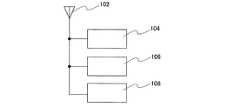
図1は、アンテナに、非接触で情報の入出力が可能(無線通信で情報の入出力が可能)な複数の集積回路が接続される半導体装置の構成を示している。図1では、アンテナ102に第1集積回路104、第2集積回路106、第3集積回路108が接続された構成を例示している。 FIG. 1 illustrates a structure of a semiconductor device in which a plurality of integrated circuits that can input and output information without contact (can input and output information by wireless communication) are connected to an antenna. FIG. 1 illustrates a configuration in which a first
図2は、図1の構成を具体化したものであり、アンテナ102と第1集積回路104、第2集積回路106、第3集積回路108が接続部109a〜109fを介してそれぞれ接続されている半導体装置100を示している。アンテナ102は、無線通信の周波数によりその形態を異ならせることができる。図2のアンテナ102は、HF帯からUHF帯(代表的には13.56MHz)に対応できる磁界型アンテナとして、スパイラルアンテナを示している。磁界型アンテナとしては、この他にもループアンテナやヘリカルアンテナを用いることができる。また、マイクロ波帯の通信周波数を用いる場合は、ダイポールアンテナやパッチアンテナを用いることができる。 FIG. 2 illustrates the configuration of FIG. 1. The
スパイラルアンテナはアンテナの巻きの回数や、アンテナの内側部分の面積により、アンテナのインピーダンスが異なるので、アンテナ102に接続する第1集積回路104、第2集積回路106、第3集積回路108のそれぞれで、実効的なアンテナ長が等しくなるように配置することが好ましい。 The spiral antenna has different antenna impedances depending on the number of windings of the antenna and the area of the inner part of the antenna. Therefore, the first
なお、アンテナは、コイルの中心軸に概略平行な方向から観察した場合に、円形、方形、三角形、及び多角形のいずれの形状を有するものであってもよい。なお、図2ではアンテナの角部(凹曲部)全てが約90度となる構成を示したがこれに限定されない。アンテナの角部(凹曲部)は、丸みを帯びた形状であっても良い。また、図2に示したアンテナの角部(凹曲部)において、直角三角形を切り取るように面取りした形状であっても良い。 The antenna may have any shape of a circle, a square, a triangle, and a polygon when observed from a direction substantially parallel to the central axis of the coil. Although FIG. 2 shows a configuration in which all the corners (concave portions) of the antenna are about 90 degrees, this is not limitative. The corner portion (concave curved portion) of the antenna may have a rounded shape. Further, the corner portion (concave curved portion) of the antenna shown in FIG. 2 may be chamfered so as to cut out a right triangle.
アンテナ102と接続する集積回路は、半導体基板(シリコンウエハー)に形成される集積回路、絶縁表面上の単結晶半導体層若しくは多結晶半導体層で形成される集積回路などを適用することができる。例えば、厚さ200nm以下の単結晶若しくは多結晶の半導体層を用いた集積回路で、当該集積回路を可撓性基板にアンテナと共に固定することで、半導体装置に柔軟性を持たせることができる。 As the integrated circuit connected to the
アンテナ102に接続する集積回路は図2で示すように、第1集積回路104、第2集積回路106、第3集積回路108として、互いに分離独立しているものを組み合わせても良いし、機能が独立していれば一体形成されているものであっても良い。製造歩留まりを考慮すると、集積回路の一つ当たりの面積が小さいものを複数個組み合わせて配設するものが好ましい。 As shown in FIG. 2, the integrated circuit connected to the
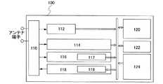
第1集積回路104、第2集積回路106、第3集積回路108は、それぞれアンテナ102に接続することで、無線ICとして機能する構成を有し、例えば、第1集積回路104、第2集積回路106、第3集積回路108は図3に示す構成を有する。図3において、集積回路は、アンテナに接続される高周波回路110(RF回路)、電源回路112、クロック及びリセット信号発生回路114、復調回路116、変調回路118、CPU120(セントラル プロセッシング ユニット)などの論理回路、ワーク領域としての揮発性メモリ122(代表的にはSRAM)、CPUのプログラムを格納する書き込み可能な不揮発性メモリ124(代表的にはEEPROM)を有する。このような構成の半導体装置により、プログラムを異ならせることで、複数の用途に対して同時に使用可能な無線ICを構成することができる。 The first
プログラムは集積回路を作製した後に書き込むことで、用途によらずに同じ回路構成のチップを生産することができ、低コストを実現することができる。つまり、多品種少量生産に適した構成である。 By writing the program after the integrated circuit is manufactured, a chip having the same circuit configuration can be produced regardless of the application, and low cost can be realized. In other words, this configuration is suitable for high-mix low-volume production.
例えば、複数の暗号に適用可能な無線ICを構成することができる。例えば、第1集積回路104の不揮発性メモリには暗号化を行わない通信に関するプログラムを格納し、第2集積回路106の不揮発性メモリには暗号方式aを用いた通信に関するプログラムを格納し、第3集積回路108の不揮発性メモリには暗号方式bを用いた通信に関するプログラムを格納した構成を有する無線ICとすることができる。 For example, a wireless IC applicable to a plurality of ciphers can be configured. For example, a non-encrypted communication program is stored in the non-volatile memory of the first
このような構成とすることで、通常の暗号化されない通信は、第1集積回路104が命令を解読し応答する。一方、暗号方式aを採用した通信は、第2集積回路106が命令を解読し応答する。また、暗号方式bを採用した通信は、第3集積回路108が命令を解読し応答する。なお、各集積回路は、サポートしない命令を受信しても応答しないようにすることで、これらの集積回路間で通信の衝突は起こらない。 By adopting such a configuration, the first
また、無線ICは複数の通信方式に対応することも可能である。例えば、図3に示すように、復調回路116と変調回路118にCPU120によって制御されるレジスタ117、レジスタ119を設け、復調信号からデータに変換する処理、およびデータの符号化処理をCPU120によって制御する構成とする。その上で、第1集積回路104には、チップの受信方式として位置変調を、応答方式としてマンチェスター符号化を用いる規格(例えばISO15693など)を用いた通信に関するプログラムを不揮発性メモリに格納し、第2集積回路106には、他の独自通信方式を用いた通信に関するプログラムを不揮発性メモリに格納した半導体装置とすることができる。 The wireless IC can also support a plurality of communication methods. For example, as shown in FIG. 3, a
このような無線ICはアンテナを集積回路と同じ基板上に形成する場合に有効である。これは、通信性能を確保するためにアンテナサイズがチップより大きい場合が多いためである。また、チップは可撓性を有することが好ましい。これは複数の集積回路を形成しチップサイズが大きくなるためである。この場合、単結晶シリコン基板やガラス基板に対し、チップは割れにくいという利点を有する。 Such a wireless IC is effective when the antenna is formed on the same substrate as the integrated circuit. This is because the antenna size is often larger than the chip in order to ensure communication performance. Moreover, it is preferable that a chip | tip has flexibility. This is because a plurality of integrated circuits are formed to increase the chip size. In this case, there is an advantage that the chip is hard to break with respect to the single crystal silicon substrate or the glass substrate.
(実施の形態2)
本実施の形態は、アンテナと複数の集積回路を有する半導体装置の一態様について図面を参照して説明する。(Embodiment 2)
In this embodiment, one embodiment of a semiconductor device including an antenna and a plurality of integrated circuits is described with reference to drawings.
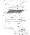
図4(A)は、本実施の形態に係る半導体装置200を示す。この半導体装置200は、アンテナ201に複数の集積回路が接続されている。図4(A)では、アンテナ201に複数の集積回路として、第1集積回路202と第2集積回路203が接続部204a〜204dを介してそれぞれ接続されている場合を示している。ここで、第1集積回路202、第2集積回路203は同じ識別符号が記憶されているものとする。つまり、第1集積回路202、第2集積回路203の識別符号が、半導体装置200の識別符号となる。 FIG. 4A shows a
リーダライタ210に接続されたアンテナ211から無線信号が出力される。当該無線信号は伝送する命令に応じて変調された電磁波である。命令を伝送するための電磁波を搬送波と呼び、無線信号を命令に応じて変調された搬送波とも呼ぶ。無線信号(命令に応じて変調された搬送波)は、半導体装置200が有するアンテナ201によって受信される。受信された無線信号の命令を第1集積回路202および第2集積回路203が処理する。処理した命令に応じて、第1集積回路202および第2集積回路203は、記憶されていた識別符号を出力する。そして、識別符号に応じて変調された搬送波は、半導体装置200のアンテナ201から、リーダライタ210のアンテナ211送信される。こうして、識別符号に応じて変調された搬送波は、アンテナ211によって受信される。そして、アンテナ211が接続されているリーダライタ210によって本発明の半導体装置200の固有識別符号が確認され制御用端末212に蓄積される。 A radio signal is output from the
半導体装置200において集積回路が1個の場合、故障や破損によって固有識別符号を認識できなくなるといった故障が発生する。しかし、本実施の形態のように、同じ識別符号を記憶した複数の集積回路を半導体装置200が備えることにより、一つの集積回路が何らかの原因で故障したり破損した場合でも、他の集積回路が正常に動作していれば、半導体装置の固有識別符号を認識することができる。 When there is one integrated circuit in the
なお、本実施の形態では、半導体装置200が同じ識別符号が記憶された第1集積回路202と第2集積回路203を有する場合を示したが、本実施の形態はそれに限定されず、複数の集積回路を備えるようにしても良い。装備する集積回路の数を増やせば、集積回路の故障や破壊に対して、冗長性を持たせることができ、より高い耐性を持つことができる。 Note that although the case where the
また、図4(A)において、半導体装置200のアンテナ201と、第1集積回路202及び第2集積回路203とが重なるように配置しているが、本実施の形態はこれに限定されず、アンテナと集積回路が重なっていなくともよい。ただし、ここでの重ならない構成とは、アンテナ201と、第1集積回路202、第2集積回路203の接続部204a〜204dは含まないものとする。アンテナ201と第1集積回路202、第2集積回路203を重ねて配置する場合、半導体装置200の中でこれらが重ならない領域A(図4、概略点線で囲む領域)が大きくなる。半導体装置200において、領域Aが大きい場合は、リーダライタ210に接続されたアンテナ211が発生する交流磁界が通りやすくなり、起電力が発生しやすくなる。半導体装置200とリーダライタ210のアンテナ211の距離が離れていても、半導体装置はアンテナ211が発生する交流磁界の影響を受けやすくなるため、半導体装置は長距離での識別が必要な場合に適している。 4A, the
一方、図4(B)のように、半導体装置200が有するアンテナ201と第1集積回路202、第2集積回路203が、接続部204a〜204dを除いて重ならない場合、半導体装置200の中で、アンテナ201、第1集積回路202、第2集積回路203以外の面積(領域A)が小さくなる。半導体装置200において、領域Aが小さい場合は、リーダライタ210に接続されたアンテナ211が発生する交流磁界が通りにくくなる。つまり、半導体装置200とリーダライタ210のアンテナ211の距離が近くなると、半導体装置200を認識させやすくなるので、他人に容易に情報が漏れることを防止することができ、情報が漏れてしまうと困る個人認証、個人情報の識別等の秘密情報の認識に適している。 On the other hand, as shown in FIG. 4B, when the
(実施の形態3)
本実施の形態は、アンテナと複数の集積回路を有する半導体装置の一態様について図面を参照して説明する。(Embodiment 3)
In this embodiment, one embodiment of a semiconductor device including an antenna and a plurality of integrated circuits is described with reference to drawings.
本実施の形態に係る半導体装置は、一つのアンテナに対し、複数の集積回路及び多数決回路を有している。この半導体図5(A)では、半導体装置300として、アンテナ301と、第1集積回路302、第2集積回路303、第3集積回路304が接続部307a〜接続部307cを介してそれぞれ接続され、アンテナ301と変調回路306が接続部307dを介して接続され、さらに第1集積回路302、第2集積回路303、第3集積回路304に多数決回路305が、図中に示す接続線を介して接続されている一例を示している。ここで、第1集積回路302、第2集積回路303、第3集積回路304は、同じ識別符号を記憶しているものとする。つまり、第1集積回路302、第2集積回路303、第3集積回路304の識別符号が、半導体装置300の固有識別符号となる。 The semiconductor device according to this embodiment includes a plurality of integrated circuits and a majority circuit for one antenna. In FIG. 5A, as the
リーダライタ210に接続されたアンテナ211から無線信号が出力される。当該無線信号は伝送する命令に応じて変調された電磁波である。命令を伝送するための電磁波を搬送波と呼び、無線信号を命令に応じて変調された搬送波とも呼ぶ。無線信号(命令に応じて変調された搬送波)は、アンテナ301によって受信される。受信された無線信号の命令は、第1集積回路302、第2集積回路303、第3集積回路304が処理する。処理した命令に応じて、第1集積回路302、第2集積回路303、第3集積回路304は、記憶していた識別符号を出力する。出力された識別符号は多数決回路305を通してから変調回路306に送られる。 A radio signal is output from the
多数決回路305の回路図を図5(C)に、真理値表を表1に示す。本実施の形態においては、三つの入力があることから、三変数の多数決回路となっている。多数決回路は三つのAND回路、すなわち第1AND回路320、第2AND回路321、第3AND回路322と、一つのOR回路323を含んでいる。 A circuit diagram of the

なお、多数決回路305は、図5(C)に示すように、複数個の信号(ここでは識別符号)に対する入力端(A〜C)を有し、その複数の入力信号に対し、多数決をとって入力数の多い信号(ここでは識別符号)を出力する出力端(X)を有する論理回路である。多数決回路305は、図5(C)において示した回路構成に限定されず、同様な機能を有するものであればどのような回路構成を用いても良い。 As shown in FIG. 5C, the
変調回路306に送られた識別符号は、識別符号に応じて変調された搬送波に変換される。そして、識別符号に応じて変調された搬送波は、アンテナ301からリーダライタ210に接続されたアンテナ211へ送信される。こうして、識別符号に応じて変調された搬送波は、アンテナ211によって受信される。そして、アンテナ211が接続されているリーダライタ210によって半導体装置300の固有識別符号が確認され、制御用端末212に蓄積される。 The identification code sent to the
本実施の形態では、何らかの要因で、同じ識別符号を記憶した三つの集積回路、すなわち、第1集積回路302、第2集積回路303、第3集積回路304のうち、一つが動作不良を起こして異なる識別符号を出力したとしても、多数決回路により排除できるため、集積回路の誤動作に対して半導体装置の冗長性を持たせることができる。 In this embodiment, for some reason, one of the three integrated circuits storing the same identification code, that is, one of the first
また、図5(A)において、半導体装置300のアンテナ301と、第1集積回路302、第2集積回路303、第3集積回路304とが重なるように配置しているが、本実施の形態はこれに限定されず、アンテナと集積回路が重なっていなくともよい。ただし、ここでの重ならない構成とは、アンテナ301と、第1集積回路302、第2集積回路303、第3集積回路304の接続部307a〜307dは含まないものとする。アンテナ301と第1集積回路302、第2集積回路303、第3集積回路304を重ねて配置する場合、半導体装置300の中でこれらが重ならない領域A(図5、概略点線で囲む領域)が大きくなる。半導体装置300において、領域Aが大きい場合は、リーダライタ210に接続されたアンテナ211が発生する交流磁界が通りやすくなり、起電力が発生しやすくなる。半導体装置200とリーダライタ210のアンテナ211の距離が離れていても、半導体装置はアンテナ211が発生する交流磁界の影響を受けやすくなるため、半導体装置は長距離での識別が必要な場合に適している。 5A, the
一方、図5(B)のように、半導体装置300が有するアンテナ301と第1集積回路302、第2集積回路303、第3集積回路304が、接続部307a〜接続部307dを除いて重ならない場合、半導体装置300の中で、アンテナ301、第1集積回路302、第2集積回路303,第3集積回路304、多数決回路305、変調回路306以外の面積(領域A)が小さくなる。半導体装置300において、領域Aが小さい場合は、リーダライタ210に接続されたアンテナ211が発生する交流磁界が通りにくくなる。つまり、半導体装置300とリーダライタ210のアンテナ211の距離が近くなると、半導体装置300を認識させやすくなるので、他人に容易に情報が漏れることを防止することができ、情報が漏れてしまうと困る個人認証、個人情報の識別等の秘密情報の認識に適している。 On the other hand, as shown in FIG. 5B, the
なお、本実施の形態では、半導体装置が三個の同じ識別符号を記憶した集積回路および多数決回路を有する場合を示したが、三個以上の集積回路を有していても良い。その場合は、複数の入力の多数決回路を使用する。半導体装置が三個以上の複数の同じ識別符号を記憶した半導体集積回路および多数決回路を有している場合は、半導体集積回路の故障や破壊に対して、より高い冗長性を持たせることができる。 Note that although the case where the semiconductor device includes the three integrated circuits and the majority circuit in which the same identification code is stored is described in this embodiment mode, the semiconductor device may include three or more integrated circuits. In that case, a majority circuit with a plurality of inputs is used. When the semiconductor device has a semiconductor integrated circuit and a majority circuit that store three or more of the same identification codes, it is possible to provide higher redundancy against failure or destruction of the semiconductor integrated circuit. .
(実施の形態4)
本実施の形態は、アンテナと集積回路の構成について図面を参照して説明する。(Embodiment 4)
In this embodiment mode, structures of an antenna and an integrated circuit are described with reference to drawings.
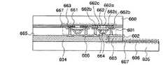
図6にアンテナと集積回路と、その接続部の構成を示す。基板600上にトランジスタを含む素子群601が形成されている。素子群601には複数のトランジスタが含まれ、配線666で回路が形成されている。さらに素子群601と電気的な接続関係にある端子部602が基板600に形成されている。そして、当該端子部602に接続するように、基板600とは別の基板605上に設けられたアンテナ606を接続する。また、アンテナ606と電気的に接続された端子部607が基板605上に形成されている。端子部607は、導電性粒子603を介して端子部602に接続されている。アンテナ606と素子群601(集積回路ともいう)に電気的に接続された接続部は、端子部602と端子部607、または、端子部602、端子部607及び導電性粒子603を含む。 FIG. 6 shows a configuration of an antenna, an integrated circuit, and a connection portion thereof. An
図6に示す構成では、素子群601のトランジスタを接続する配線の一部を端子部602として用いている。そして、アンテナ606の端子部607が、端子部602に接続するように、基板600と、アンテナ606が設けられた基板605とを貼り合わせている。基板600と基板605の間には、導電性粒子603と樹脂604が設けられている。導電性粒子603によって、アンテナ606の端子部607と端子部602とは電気的に接続されている。 In the configuration illustrated in FIG. 6, part of the wiring that connects the transistors in the
素子群601の構成及び作製方法について説明する。素子群601は、大面積の基板上に複数形成し、その後、分断することで完成させれば、安価なものを提供することができる。基板600としては、例えばバリウムホウケイ酸ガラスや、アルミノホウケイ酸ガラスなどのガラス基板、石英基板、セラミック基板等を用いることができる。また、半導体基板の表面に絶縁膜を形成したものを用いても良い。プラスチック等の可撓性を有する合成樹脂からなる基板を用いても良い。基板の表面を、CMP法などの研磨により平坦化しておいても良い。また、ガラス基板、石英基板や、半導体基板を研磨して薄くした基板を用いてもよい。 A structure and a manufacturing method of the
基板600上に設けられている下地層661としては、酸化珪素や、窒化珪素または窒化酸化珪素などの絶縁膜を用いることができる。下地層661によって、基板600に含まれるNaなどのアルカリ金属やアルカリ土類金属が半導体層662に拡散しトランジスタの特性に悪影響をおよぼすのを防ぐことができる。図6では、下地層661を単層の構造としているが、2層あるいはそれ以上の複数層で形成してもよい。なお、石英基板など不純物の拡散がさして問題とならない場合は、下地層661を必ずしも設ける必要はない。 As the
なお、高密度プラズマによって基板600の表面を直接処理してもよい。高密度プラズマは、マイクロ波、例えば2.45GHzを使うことによって生成される。なお、高密度プラズマとしては電子密度が1011〜1013/cm3かつ電子温度が2eV以下、イオンエネルギーが5eV以下であるものを用いる。このように低電子温度が特徴である高密度プラズマは、活性種の運動エネルギーが低いため、従来のプラズマ処理に比べプラズマダメージが少なく欠陥が少ない膜を形成することができる。プラズマの生成はラジアルスロットアンテナを用いたマイクロ波励起のプラズマ処理装置を用いることができる。マイクロ波を発生するアンテナから基板600までの距離を20〜80mm(好ましくは20〜60mm)とする。窒化性雰囲気、例えば、窒素(N)と希ガス(He、Ne、Ar、Kr、Xeの少なくとも一つを含む)雰囲気下、または窒素と水素(H)と希ガス雰囲気下、またはアンモニア(NH3)と希ガス雰囲気下において、上記高密度プラズマ処理を行うことによって、基板600表面を窒化することができる。基板600としてガラスや石英、シリコンウエハー等を用いた場合、基板600の表面に形成された窒化物層は窒化珪素を主成分とするので、基板600側から拡散してくる不純物のブロッキング層として利用することができる。この窒化物層の上に酸化珪素膜または酸窒化珪素膜をプラズマCVD法で形成して下地層661としても良い。Note that the surface of the
また、酸化珪素や酸窒化珪素などからなる下地層661の表面に対し同様な高密度プラズマ処理を行うことにより、その表面及び表面から1〜10nmの深さを窒化処理することができる。このきわめて薄い窒化珪素の層は、ブロッキング層として機能し、且つその上に形成する半導体層662へ与える応力の影響が少ないので好ましい。 Further, by performing similar high-density plasma treatment on the surface of the
半導体層662としては、単結晶半導体層や多結晶半導体層を用いることができる。多結晶半導体層は非晶質半導体膜を結晶化して得ることができる。結晶化方法としては、レーザ結晶化法、RTA又はファーネスアニール炉を用いる熱結晶化法、結晶化を助長する金属元素を用いる熱結晶化法等を用いることができる。半導体層662は、チャネル形成領域662aと、導電型を付与する不純物元素が添加された一対の不純物領域662bとを有する。なお、チャネル形成領域662aと一対の不純物領域662bとの間に、不純物領域662bよりも低濃度で前記不純物元素が添加された低濃度不純物領域662cを有する構成を示したがこれに限定されない。低濃度不純物領域662cを設けない構成であってもよい。トランジスタのチャネル形成領域662aにおいて、導電型を付与する不純物元素が添加されていてもよい。こうして、トランジスタのしきい値電圧を制御することができる。 As the
第1の絶縁層663としては、酸化珪素、窒化珪素または窒化酸化珪素等を用い、単層または複数の膜を積層させて形成することができる。この場合において、第1の絶縁層663の表面を酸化雰囲気又は窒化雰囲気で高密度プラズマによって処理し、酸化又は窒化処理して緻密化しても良い。高密度プラズマは、前述と同様に、マイクロ波、例えば2.45GHzを使うことによって生成される。なお、高密度プラズマとしては電子密度が1011〜1013/cm3かつ電子温度が2eV以下、イオンエネルギーが5eV以下であるものを用いる。プラズマの生成はラジアルスロットアンテナを用いたマイクロ波励起のプラズマ処理装置を用いることができる。The first insulating
第1の絶縁層663を成膜する前に、半導体層662の表面に対して上記高密度プラズマ処理を行って、半導体層の表面を酸化又は窒化処理してもよい。このとき、基板600の温度を300〜450℃とし、酸化雰囲気又は窒化雰囲気で処理することにより、その上に堆積する第1の絶縁層663と良好な界面を形成することができる。窒化雰囲気としては、窒素(N)と希ガス(He、Ne、Ar、Kr、Xeの少なくとも一つを含む)雰囲気下、または窒素と水素(H)と希ガス雰囲気下、またはアンモニア(NH3)と希ガス雰囲気を用いることができる。酸化雰囲気としては、酸素(O)と希ガス雰囲気下、または酸素と水素(H)と希ガス雰囲気下、または一酸化二窒素(N2O)と希ガス雰囲気を用いることができる。Before the first insulating
ゲート電極664としては、Ta、W、Ti、Mo、Al、Cu、Cr、Ndから選ばれた一種の元素または当該元素を複数含む合金若しくは化合物からなる、単層または積層構造を用いることができる。図6では、2層構造のゲート電極664を示す。 As the
トランジスタは、半導体層662と、ゲート電極664と、半導体層662とゲート電極664との間のゲート絶縁膜として機能する第1の絶縁層663とによって構成される。図6では、トランジスタをトップゲート型のトランジスタとして示したが、半導体層の下方にゲート電極を有するボトムゲート型のトランジスタであっても良いし、半導体層の上下にゲート電極を有するデュアルゲート型のトランジスタであっても良い。 The transistor includes a
第2の絶縁層667は窒化珪素膜などイオン性不純物をブロッキングするバリア性の絶縁膜であることが望ましい。第2の絶縁層667は窒化珪素または酸窒化珪素で形成する。この第2の絶縁層667は、半導体層662の汚染を防ぐ保護膜としての機能を有している。第2の絶縁層667を堆積した後に、水素ガスを導入して前述のような高密度プラズマ処理をすることで、第2の絶縁層667の水素化を行っても良い。または、アンモニア(NH3)ガスを導入して、第2の絶縁層667の窒化と水素化を行っても良い。または、酸素、一酸化二窒素(N2O)ガスなどと水素ガスを導入して、酸化窒化処理と水素化処理を行っても良い。この方法により、窒化処理、酸化処置若しくは酸化窒化処理を行うことにより第2の絶縁層667の表面を緻密化することができる。こうして第2の絶縁層667の保護膜としての機能を強化することができる。第2の絶縁層667に導入された水素は、その後400〜450℃の熱処理をすることにより放出されて、半導体層662の水素化をすることができる。なお当該水素化処理は、第1の絶縁層663に導入された水素を用いた水素化処理と組み合わせてもよい。The second
第3の絶縁層665としては、無機絶縁膜や有機絶縁膜の単層または積層構造を用いることができる。無機絶縁膜としては、CVD法により形成された酸化珪素膜や、SOG(Spin On Glass)法により塗布された酸化珪素膜などを用いることができ、有機絶縁膜としてはポリイミド、ポリアミド、BCB(ベンゾシクロブテン)、アクリルまたはポジ型感光性有機樹脂、ネガ型感光性有機樹脂等の膜を用いることができる。また、第3の絶縁層665として、珪素(Si)と酸素(O)との結合で骨格構造が構成される材料を用いることもできる。この材料の置換基として、少なくとも水素を含む有機基(例えばアルキル基、芳香族炭化水素)が用いられる。置換基として、フルオロ基を用いてもよい。または置換基として、少なくとも水素を含む有機基と、フルオロ基とを用いてもよい。 As the third insulating
配線666としては、Al、Ni、W、Mo、Ti、Pt、Cu、Ta、Au、Mnから選ばれた一種の元素または当該元素を複数含む合金からなる、単層または積層構造を用いることができる。配線666は、トランジスタのソースやドレインと接続される配線となると共に、端子部602となる。 As the
アンテナ606は、Au、Ag、Cuなどのナノ粒子を含む導電性ペーストを用いて、インクジェット印刷法やスクリーン印刷法などの印刷技術を用いて形成することもできる。また、ディスペンサ方式等の液滴を吐出してパターンを形成することができる。このような方法により、材料の利用効率の向上等の利点を有する。 The
また、素子群601は基板600上に形成されたもの(図7(A)参照)をそのまま使用してもよいが、基板600上の素子群601を剥離し(図7(B)参照)、当該素子群601をフレキシブル基板701に貼り合わせてもよい(図7(C)参照)。フレキシブル基板701は、柔軟性を有し、例えば、ポリカーボネート、ポリアリレート、ポリエーテルスルフォン等のプラスチック基板またはセラミック基板等を用いることができる。 Further, the
基板600からの素子群601の剥離は、(A)あらかじめ基板600と素子群601との間に剥離層を設けておいて、剥離層をエッチング剤により除去することで行う方法か、(B)剥離層をエッチング剤により部分的に除去し、その後、基板600と素子群601とを物理的に剥離する方法か、(C)素子群601が形成された耐熱性の高い基板600を機械的に削除又は溶液やガスによるエッチングで除去することで、当該素子群601を切り離す方法を用いることができる。なお、物理的手段によって剥離されるとは、外部からストレスが与えられて剥離されることを指し、例えば、ノズルから吹き付けられるガスの風圧や超音波等からストレスを与えられて剥離することである。 Peeling of the
上記(A)や(B)のより具体的な方法としては、耐熱性の高い基板600と素子群601の間に金属酸化膜を設け、当該金属酸化膜を結晶化により脆弱化して、当該素子群601を剥離する方法や、耐熱性の高い基板600と素子群601の間に水素を含む非晶質珪素膜を設け、レーザ−光の照射またはエッチングにより当該非晶質珪素膜を除去することで、当該素子群601を剥離する方法が挙げられる。剥離した素子群601のフレキシブル基板701への貼り付けは、市販の接着剤を用いればよく、例えば、エポキシ樹脂系接着剤や樹脂添加剤等の接着材を用いればよい。 As a more specific method of the above (A) or (B), a metal oxide film is provided between the
素子群601をアンテナが形成されたフレキシブル基板701に貼り合わせ当該アンテナとの電気的接続をとると、厚さが薄く、軽く、落下しても割れにくい半導体装置が完成する(図7(C)参照)。安価なフレキシブル基板701を用いると、安価な半導体装置を提供することができる。さらに、フレキシブル基板701は可撓性を有するため、曲面や異形の形状上に貼り合わせることが可能となり、多種多様の用途が実現する。例えば、薬の瓶のような曲面上に、本発明の半導体装置の一形態である集積回路を密着して貼り合わせることができる(図7(D)参照)。さらに、基板600を再利用すれば、低コストで半導体装置を作製することができる。 When the
素子群601は、フィルムで覆うことによって封止することができる。当該フィルムの表面は、二酸化珪素(シリカ)の粉末により、コーティングされていてもよい。コーティングにより、高温で高湿度の環境下においても防水性を保つことができる。つまり、耐湿性の機能を持たせることができる。また、当該フィルムの表面に帯電防止の機能を持たせてもよい。また、当該フィルムの表面は、炭素を主成分とする材料(例えば、ダイヤモンドライクカーボン)によりコーティングされていてもよい。コーティングにより強度が増し、半導体装置の劣化や破壊を抑制することができる。また、フィルムは、基材の材料(例えば樹脂)と、二酸化珪素や導電性材料や炭素を主成分とする材料とを混ぜ合わせた材料により形成してもよい。また、フィルムに界面活性剤を表面に塗布する、もしくは界面活性剤を直接練り込むことで帯電防止の機能を持たせることができる。 The
(実施の形態5)
本実施の形態では、集積回路が形成された薄片を可撓性基板と組み合わせる半導体装置の構成について図面を参照して説明する。(Embodiment 5)
In this embodiment mode, a structure of a semiconductor device in which a thin piece over which an integrated circuit is formed is combined with a flexible substrate will be described with reference to drawings.
図8(A)において、本発明の半導体装置は、可撓性を有する保護層901と、アンテナ902を含む可撓性を有する保護層903と、剥離プロセスや基板の薄膜化により形成された素子群904とを有する。素子群904は、実施の形態3で素子群601として示した構成と同様の構成とすることができる。保護層903上に形成されたアンテナ902は、素子群904と電気的に接続する。図8(A)では、アンテナ902は保護層903上にのみ形成されているが、本発明はこの構成に制約されず、アンテナ902を保護層901上にも形成してもよい。なお、素子群904と、保護層901及び保護層903との間には、窒化珪素膜等からなるバリア膜を形成するとよい。そうすると、素子群904が汚染されることなく、信頼性を向上させた半導体装置を提供することができる。 8A, a semiconductor device of the present invention includes a flexible
アンテナ902は、Ag、Cu、またはそれらでメッキされた金属で形成することができる。素子群904とアンテナ902とは、異方性導電膜を用い、紫外線処理又は超音波処理を行うことで接続することができる。なお、素子群904とアンテナ902とは、導電性ペースト等を用いて接着してもよい。保護層901及び保護層903によって素子群904を挟むことによって半導体装置が完成する(図8(A)中、矢印参照)。 The
こうして形成された半導体装置の断面構造を図8(B)に示す。挟まれた素子群904の厚さは、5μm以下、好ましくは0.1μm〜3μmの厚さを有するように形成するとよい。また、保護層901及び保護層903を重ねたときの厚さをdとしたとき、保護層901及び保護層903の厚さは、好ましくは(d/2)±30μm、さらに好ましくは(d/2)±10μmとする。また、保護層901及び保護層903の厚さは10μm〜200μmであることが望ましい。さらに、素子群904の面積は10mm角(100mm2)以下であり、望ましくは0.3mm角〜4mm角(0.09mm2〜16mm2)の面積とするとよい。A cross-sectional structure of the semiconductor device thus formed is shown in FIG. The thickness of the sandwiched
保護層901及び保護層903は、有機樹脂材料で形成されているため、折り曲げに対して強い特性を有する。また、剥離プロセスや基板の薄膜化により形成した素子群904自体も、単結晶半導体に比べて、折り曲げに対して強い特性を有する。そして、素子群904と、保護層901及び保護層903とは空隙がないように、密着させることができるため、完成した半導体装置自体も折り曲げに対して強い特性を有する。このような保護層901及び保護層903で囲われた素子群904は、他の個体物の表面または内部に配置しても良いし、紙の中に埋め込んでも良い。 Since the
素子群904を有する半導体装置を曲面を有する基板に貼る場合について説明する。説明には図8(C)を用いる。図8(C)では、素子群904から選択された1つのトランジスタ981を図示する。トランジスタ981は、ゲート電極907の電位に応じて、ソースまたはドレインの一方905からソースまたはドレインの他方906に電流を流す。トランジスタ981の電流が流れる方向(キャリアの移動方向)と、基板980が弧を描く方向が直交するように、トランジスタ981は配置される。このような配置にすれば、基板980が折り曲げられて弧を描いても、トランジスタ981に与えられる応力の影響が少なく、素子群904が含むトランジスタ981の特性の変動を抑制することができる。 A case where a semiconductor device including the
(実施の形態6)
本実施の形態では、非接触で情報の送受信が可能な半導体装置(無線ICともいう)の用途について図9及び図10を用いて説明する。無線IC700は、例えば、紙幣、硬貨、有価証券類、無記名債券類、証書類(運転免許証や住民票等、図10(A)参照)、包装用容器類(包装紙やボトル等、図10(B)参照)、DVDソフトやCDやビデオテープ等の記録媒体(図10(C)参照)、車やバイクや自転車等の乗物類(図10(D)参照)、鞄や眼鏡等の身の回り品(図10(E)参照)、食品類、衣類、生活用品類、電子機器等に設けて使用することができる。電子機器とは、液晶表示装置、EL(エレクトロルミネッセンス)表示装置、テレビジョン装置(単にテレビまたはテレビ受像器とも呼ぶ)および携帯電話機等を指す。(Embodiment 6)
In this embodiment, application of a semiconductor device (also referred to as a wireless IC) that can transmit and receive information without contact is described with reference to FIGS. The
無線IC700は、物品の表面に貼り付けたり、物品に埋め込んだりして物品に固定することができる。例えば、本なら紙に埋め込んだり、有機樹脂からなるパッケージなら当該有機樹脂に埋め込んだりするとよい。紙幣、硬貨、有価証券類、無記名債券類、証書類等に無線IC700を設けることにより、偽造を防止することができる。また、包装用容器類、記録媒体、身の回り品、食品類、衣類、生活用品類、電子機器等に無線IC700を設けることにより、検品システムやレンタル店のシステムなどの効率化を図ることができる。また乗物類に無線IC700を設けることにより、偽造や盗難を防止することができる。また、動物等の生き物に埋め込むことによって、個々の生き物の識別を容易に行うことができる。例えば、家畜等の生き物に無線ICを埋め込むことによって、生まれた年や性別または種類等を容易に識別することが可能となる。 The
以上のように、本発明の無線IC700は物品(生物を含む)であればどのようなものにでも設けて使用することができ、無線IC700を有する物品が壊れやすい環境においても有効である。 As described above, the
無線IC700は、無線通信によるデータの送受信が可能である点、様々な形状に加工可能である点、選択する周波数によっては、指向性が広く、認識範囲が広い点等の様々な利点を有する。 The
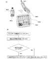
次に、無線IC700を用いたシステムの一形態について、図9を用いて説明する。表示部9521を含む携帯端末の側面には、リーダライタ9520が設けられ、物品A9522の側面には本発明の半導体装置9523(無線IC700)が設けられ、物品B9532の上面には本発明の半導体装置9531が設けられている(図9(A)参照)。物品A9522が含む半導体装置9523にリーダライタ9520をかざすと、表示部9521に物品A9522の原材料や原産地、生産工程ごとの検査結果や流通過程の履歴、商品の説明等の商品に関する情報が表示される。物品B9532が含む半導体装置9531にリーダライタ9520をかざすと、表示部9521に物品B9532の原材料や原産地、生産工程ごとの検査結果や流通過程の履歴、商品の説明等の商品に関する情報が表示される。 Next, one mode of a system using the
図9(A)に示すシステムを利用したビジネスモデルの一例を示す。説明には図9(B)のフローチャートを用いる。携帯端末において、アレルギーの情報を入力しておく(ステップ1)。アレルギーの情報とは、所定の人物がアレルギー反応を起こす医薬品またはその成分等の情報である。携帯端末に設けられたリーダライタ9520によって、前述のとおり物品A9522の情報を取得する(ステップ2)。ここで、物品A9522は医薬品であるとする。物品A9522の情報には物品A9522の成分等の情報が含まれる。アレルギーの情報と取得した物品A9522の成分等の情報とを比較し、一致するか否かを判断する(ステップ3)。一致する場合、所定の人物は物品Aに対してアレルギー反応を起こす危険性があるとし、携帯端末の使用者に注意を呼びかける(ステップ4)。一致しない場合、所定の人物は物品Aに対してアレルギー反応を起こす危険性が少ないとし、携帯端末の使用者にその旨(安全である旨)を知らせる(ステップ5)。ステップ4やステップ5において、携帯端末の使用者に情報を知らせる方法は、携帯端末の表示部9521に表示を行う方法であっても良いし、携帯端末のアラーム等を鳴らす方法であっても良い。 An example of a business model using the system shown in FIG. The flowchart of FIG. 9B is used for the description. In the portable terminal, allergy information is input (step 1). The allergy information is information on pharmaceuticals or components thereof that cause a predetermined person to cause an allergic reaction. Information on the
また、別のビジネスモデルの例として、端末に、同時に使用すると危険な医薬品または同時に使用すると危険な医薬品の成分の組み合わせの情報(以下、組み合わせ情報という)を入力しておく(ステップ1)。端末に設けられたリーダライタによって、前述のとおり物品Aの情報を取得する(ステップ2)。ここで、物品Aは医薬品であるとする。物品Aの情報には物品Aの成分等の情報が含まれる。次いで、端末に設けられたリーダライタによって、前述のとおり物品Bの情報を取得する(ステップ2’)。ここで、物品Bも医薬品であるとする。物品Bの情報には物品Bの成分等の情報が含まれる。こうして、複数の医薬品の情報を取得する。組み合わせ情報と取得した複数の物品の情報とを比較し、一致するか否か、即ち、同時に使用すると危険な医薬品の成分の組み合わせが有るか否かを判断する(ステップ3)。一致する場合、端末の使用者に注意を呼びかける(ステップ4)。一致しない場合、端末の使用者にその旨(安全である旨)を知らせる(ステップ5)。ステップ4やステップ5において、端末の使用者に情報を知らせる方法は、端末の表示部に表示を行う方法であっても良いし、携帯端末のアラーム等を鳴らす方法であっても良い。 As another example of the business model, information on a combination of dangerous drugs that are used at the same time or a combination of ingredients that are dangerous when used at the same time (hereinafter referred to as combination information) is input to the terminal (step 1). The information on the article A is acquired by the reader / writer provided in the terminal as described above (step 2). Here, it is assumed that the article A is a medicine. The information on the article A includes information such as the components of the article A. Next, the information on the article B is acquired by the reader / writer provided in the terminal as described above (step 2 '). Here, it is assumed that the article B is also a medicine. The information on the article B includes information such as the component of the article B. Thus, information on a plurality of medicines is acquired. The combination information is compared with the acquired information of the plurality of articles, and it is determined whether or not they match, that is, whether or not there is a combination of components of pharmaceuticals that are dangerous when used at the same time (step 3). If they match, the terminal user is alerted (step 4). If they do not match, the terminal user is informed of that fact (safe) (step 5). In step 4 or step 5, the method of notifying the user of the terminal may be a method of displaying on the display unit of the terminal, or a method of sounding an alarm of the portable terminal.
このように、システムに本発明の半導体装置を活用することで、情報の取得を簡単に行うことができ、高機能化と高付加価値化を実現したシステムを提供することができる。 In this manner, by utilizing the semiconductor device of the present invention for the system, information can be easily acquired, and a system that realizes high functionality and high added value can be provided.
100 半導体装置
102 アンテナ
104 第1集積回路
106 第2集積回路
108 第3集積回路
109a 接続部
109b 接続部
109c 接続部
109d 接続部
109e 接続部
109f 接続部
110 高周波回路
112 電源回路
114 クロック及びリセット信号発生回路
116 復調回路
117 レジスタ
118 変調回路
119 レジスタ
120 CPU
122 揮発性メモリ
124 不揮発性メモリ
200 半導体装置
201 アンテナ
202 第1集積回路
203 第2集積回路
204a 接続部
204b 接続部
204c 接続部
204d 接続部
210 リーダライタ
211 アンテナ
212 制御用端末
300 半導体装置
301 アンテナ
302 第1集積回路
303 第2集積回路
304 第3集積回路
305 多数決回路
306 変調回路
307a 接続部
307b 接続部
307c 接続部
307d 接続部
320 第1AND回路
321 第2AND回路
322 第3AND回路
323 OR回路
600 基板
601 素子群
602 端子部
603 導電性粒子
604 樹脂
605 基板
606 アンテナ
607 端子部
661 下地層
662 半導体層
662a チャネル形成領域
662b 不純物領域
662c 低濃度不純物領域
663 第1の絶縁層
664 ゲート電極
665 第3の絶縁層
666 配線
667 第2の絶縁層
700 無線IC
701 フレキシブル基板
901 保護層
902 アンテナ
903 保護層
904 素子群
905 ソースまたはドレインの一方
906 ソースまたはドレインの他方
907 ゲート電極
980 基板
981 トランジスタ
9520 リーダライタ
9521 表示部
9522 物品A
9523 半導体装置
9531 半導体装置
9532 物品BDESCRIPTION OF
122
701
9523
Claims (8)
Translated fromJapanese前記アンテナに接続された複数の集積回路を有し、
前記複数の集積回路は、それぞれ、識別符号と集積回路の動作を制御するプログラムが記憶された記憶回路を有し、
前記識別符号は、前記複数の集積回路のぞれぞれで異なり、
前記プログラムは、前記複数の集積回路のそれぞれで異なることを特徴とする半導体装置。An antenna,
A plurality of integrated circuits connected to the antenna;
Each of the plurality of integrated circuits includes a storage circuit in which an identification code and a program for controlling the operation of the integrated circuit are stored.
The identification code is different for each of the plurality of integrated circuits,
The semiconductor device is characterized in that the program is different for each of the plurality of integrated circuits.
前記アンテナに接続された複数の集積回路を有し、
前記複数の集積回路は、それぞれ、識別符号と集積回路の動作を制御するプログラムが記憶された記憶回路を有し、
前記複数の集積回路から選択された少なくとも2つの集積回路は、同じ識別符号と同じプログラムを有することを特徴とする半導体装置。An antenna,
A plurality of integrated circuits connected to the antenna;
Each of the plurality of integrated circuits includes a storage circuit in which an identification code and a program for controlling the operation of the integrated circuit are stored.
At least two integrated circuits selected from the plurality of integrated circuits have the same identification code and the same program.
前記アンテナに接続された複数の集積回路と、
前記複数の集積回路に接続された多数決回路を有し、
前記複数の集積回路は、それぞれ、識別符号と集積回路の動作を制御するプログラムが記憶された記憶回路を有し、
前記複数の集積回路から選択された少なくとも2つの集積回路は、同じ識別符号と同じプログラムを有し、
前記多数決回路は、前記複数の集積回路の通信に応じた複数の個体情報の識別符号より、当該識別符号の多数決値である識別符号を出力し、
前記アンテナは、前記多数決値である識別符号を基に変調された搬送波を出力することを特徴とする半導体装置。An antenna,
A plurality of integrated circuits connected to the antenna;
A majority circuit connected to the plurality of integrated circuits;
Each of the plurality of integrated circuits includes a storage circuit in which an identification code and a program for controlling the operation of the integrated circuit are stored.
At least two integrated circuits selected from the plurality of integrated circuits have the same identification code and the same program;
The majority circuit outputs an identification code, which is a majority value of the identification code, from identification codes of a plurality of individual information corresponding to communication of the plurality of integrated circuits,
The semiconductor device according to claim 1, wherein the antenna outputs a carrier wave modulated based on an identification code which is the majority value.
前記アンテナは、前記複数の集積回路とは異なる基板上に形成されることを特徴とする半導体装置。In any one of Claims 1 thru | or 3,
The semiconductor device is characterized in that the antenna is formed on a different substrate from the plurality of integrated circuits.
前記アンテナの形状は、ループ状またはスパイラル状であることを特徴とする半導体装置。In any one of Claims 1 thru | or 4,
The antenna device has a loop shape or a spiral shape.
前記複数の集積回路は、前記アンテナと重なるように配置されることを特徴とする半導体装置。In any one of Claims 1 thru | or 5,
The semiconductor device, wherein the plurality of integrated circuits are arranged to overlap the antenna.
前記複数の集積回路は、前記アンテナと重ならないように配置されることを特徴とする半導体装置。In any one of Claims 1 thru | or 5,
The semiconductor device, wherein the plurality of integrated circuits are arranged so as not to overlap with the antenna.
前記複数の集積回路は、前記アンテナと重ならず、且つ、当該アンテナの内側に配置されることを特徴とすることを特徴とする半導体装置。In any one of Claims 1 thru | or 5,
The semiconductor device is characterized in that the plurality of integrated circuits do not overlap with the antenna and are disposed inside the antenna.
Priority Applications (1)
| Application Number | Priority Date | Filing Date | Title |
|---|---|---|---|
| JP2006241019AJP2007109216A (en) | 2005-09-13 | 2006-09-06 | Semiconductor device |
Applications Claiming Priority (2)
| Application Number | Priority Date | Filing Date | Title |
|---|---|---|---|
| JP2005266122 | 2005-09-13 | ||
| JP2006241019AJP2007109216A (en) | 2005-09-13 | 2006-09-06 | Semiconductor device |
Publications (2)
| Publication Number | Publication Date |
|---|---|
| JP2007109216Atrue JP2007109216A (en) | 2007-04-26 |
| JP2007109216A5 JP2007109216A5 (en) | 2009-10-15 |
Family
ID=38035008
Family Applications (1)
| Application Number | Title | Priority Date | Filing Date |
|---|---|---|---|
| JP2006241019AWithdrawnJP2007109216A (en) | 2005-09-13 | 2006-09-06 | Semiconductor device |
Country Status (1)
| Country | Link |
|---|---|
| JP (1) | JP2007109216A (en) |
Cited By (16)
| Publication number | Priority date | Publication date | Assignee | Title |
|---|---|---|---|---|
| JP2009016805A (en)* | 2007-06-07 | 2009-01-22 | Semiconductor Energy Lab Co Ltd | Semiconductor device |
| JP2009207129A (en)* | 2008-01-31 | 2009-09-10 | Semiconductor Energy Lab Co Ltd | Semiconductor device |
| JP2010067128A (en)* | 2008-09-12 | 2010-03-25 | Nittoku Eng Co Ltd | Noncontact information processing medium |
| JP2010122852A (en)* | 2008-11-19 | 2010-06-03 | Universal Entertainment Corp | Game medium and game system |
| JP2011070321A (en)* | 2009-09-24 | 2011-04-07 | Maxell Seiki Kk | Multi-application ic card, and ic card |
| JP2011516933A (en)* | 2007-10-28 | 2011-05-26 | テゴ,インコーポレイテッド | Method and system for sharing power in a multiple radio frequency network node RFID tag |
| US8558699B2 (en) | 2005-12-09 | 2013-10-15 | Tego Inc. | Multiple radio frequency network node RFID tag |
| US8941470B2 (en) | 2005-12-09 | 2015-01-27 | Tego Inc. | Methods and systems of a radio frequency network node RFID tag with hardened memory system |
| US8988223B2 (en) | 2005-12-09 | 2015-03-24 | Tego Inc. | RFID drive management facility |
| US9117128B2 (en) | 2005-12-09 | 2015-08-25 | Tego, Inc. | External access to memory on an RFID tag |
| KR101554695B1 (en) | 2012-10-05 | 2015-09-21 | 가부시키가이샤 무라타 세이사쿠쇼 | Communication terminal device |
| US9361568B2 (en) | 2005-12-09 | 2016-06-07 | Tego, Inc. | Radio frequency identification tag with hardened memory system |
| US9418263B2 (en) | 2005-12-09 | 2016-08-16 | Tego, Inc. | Operating systems for an RFID tag |
| US9430732B2 (en) | 2014-05-08 | 2016-08-30 | Tego, Inc. | Three-dimension RFID tag with opening through structure |
| US9542577B2 (en) | 2005-12-09 | 2017-01-10 | Tego, Inc. | Information RFID tagging facilities |
| US9953193B2 (en) | 2014-09-30 | 2018-04-24 | Tego, Inc. | Operating systems for an RFID tag |
Citations (5)
| Publication number | Priority date | Publication date | Assignee | Title |
|---|---|---|---|---|
| JPH10187550A (en)* | 1996-12-26 | 1998-07-21 | Rohm Co Ltd | Ic card |
| WO1999032304A1 (en)* | 1997-12-22 | 1999-07-01 | Hitachi, Ltd. | Semiconductor device |
| JP2002083277A (en)* | 2000-09-07 | 2002-03-22 | Mitsubishi Materials Corp | Data carrier |
| JP2003346117A (en)* | 2000-06-30 | 2003-12-05 | Hitachi Maxell Ltd | Non-contact communication information carrier |
| JP2005244212A (en)* | 2004-01-30 | 2005-09-08 | Semiconductor Energy Lab Co Ltd | Semiconductor device |
- 2006
- 2006-09-06JPJP2006241019Apatent/JP2007109216A/ennot_activeWithdrawn
Patent Citations (5)
| Publication number | Priority date | Publication date | Assignee | Title |
|---|---|---|---|---|
| JPH10187550A (en)* | 1996-12-26 | 1998-07-21 | Rohm Co Ltd | Ic card |
| WO1999032304A1 (en)* | 1997-12-22 | 1999-07-01 | Hitachi, Ltd. | Semiconductor device |
| JP2003346117A (en)* | 2000-06-30 | 2003-12-05 | Hitachi Maxell Ltd | Non-contact communication information carrier |
| JP2002083277A (en)* | 2000-09-07 | 2002-03-22 | Mitsubishi Materials Corp | Data carrier |
| JP2005244212A (en)* | 2004-01-30 | 2005-09-08 | Semiconductor Energy Lab Co Ltd | Semiconductor device |
Cited By (32)
| Publication number | Priority date | Publication date | Assignee | Title |
|---|---|---|---|---|
| US9424447B2 (en) | 2005-12-09 | 2016-08-23 | Tego, Inc. | RFID tag facility with access to a sensor |
| US8988223B2 (en) | 2005-12-09 | 2015-03-24 | Tego Inc. | RFID drive management facility |
| US10691992B2 (en) | 2005-12-09 | 2020-06-23 | Tego, Inc. | RF tag with memory management |
| US10430702B2 (en) | 2005-12-09 | 2019-10-01 | Tego, Inc. | RF tag network connectivity through gateway facility |
| US9858452B2 (en) | 2005-12-09 | 2018-01-02 | Tego, Inc. | Information RFID tagging facilities |
| US9842290B2 (en) | 2005-12-09 | 2017-12-12 | Tego, Inc. | Flight-cycle sensor monitoring of aviation component |
| US8558699B2 (en) | 2005-12-09 | 2013-10-15 | Tego Inc. | Multiple radio frequency network node RFID tag |
| US8941470B2 (en) | 2005-12-09 | 2015-01-27 | Tego Inc. | Methods and systems of a radio frequency network node RFID tag with hardened memory system |
| US9405950B2 (en) | 2005-12-09 | 2016-08-02 | Tego, Inc. | External access to memory on an RFID tag |
| US9465559B2 (en) | 2005-12-09 | 2016-10-11 | Tego, Inc. | System and method for emulating many time programmable memory |
| US9117128B2 (en) | 2005-12-09 | 2015-08-25 | Tego, Inc. | External access to memory on an RFID tag |
| US9710682B2 (en) | 2005-12-09 | 2017-07-18 | Tego, Inc. | Operating systems for an RFID tag |
| US9361568B2 (en) | 2005-12-09 | 2016-06-07 | Tego, Inc. | Radio frequency identification tag with hardened memory system |
| US9390362B2 (en) | 2005-12-09 | 2016-07-12 | Tego, Inc. | Radio frequency identification tag with emulated multiple-time programmable memory |
| US9594998B2 (en) | 2005-12-09 | 2017-03-14 | Tego, Inc. | Radio frequency identification tag with hardened memory system |
| US9542577B2 (en) | 2005-12-09 | 2017-01-10 | Tego, Inc. | Information RFID tagging facilities |
| US8947233B2 (en) | 2005-12-09 | 2015-02-03 | Tego Inc. | Methods and systems of a multiple radio frequency network node RFID tag |
| US9418263B2 (en) | 2005-12-09 | 2016-08-16 | Tego, Inc. | Operating systems for an RFID tag |
| US9471821B2 (en) | 2005-12-09 | 2016-10-18 | Tego, Inc. | External access to memory on an RFID tag |
| JP2009016805A (en)* | 2007-06-07 | 2009-01-22 | Semiconductor Energy Lab Co Ltd | Semiconductor device |
| JP2011516933A (en)* | 2007-10-28 | 2011-05-26 | テゴ,インコーポレイテッド | Method and system for sharing power in a multiple radio frequency network node RFID tag |
| US9460377B2 (en) | 2008-01-31 | 2016-10-04 | Semiconductor Energy Laboratory Co., Ltd. | Semiconductor device |
| JP2009207129A (en)* | 2008-01-31 | 2009-09-10 | Semiconductor Energy Lab Co Ltd | Semiconductor device |
| JP2010067128A (en)* | 2008-09-12 | 2010-03-25 | Nittoku Eng Co Ltd | Noncontact information processing medium |
| JP2010122852A (en)* | 2008-11-19 | 2010-06-03 | Universal Entertainment Corp | Game medium and game system |
| JP2011070321A (en)* | 2009-09-24 | 2011-04-07 | Maxell Seiki Kk | Multi-application ic card, and ic card |
| KR101554695B1 (en) | 2012-10-05 | 2015-09-21 | 가부시키가이샤 무라타 세이사쿠쇼 | Communication terminal device |
| US9430732B2 (en) | 2014-05-08 | 2016-08-30 | Tego, Inc. | Three-dimension RFID tag with opening through structure |
| US9953193B2 (en) | 2014-09-30 | 2018-04-24 | Tego, Inc. | Operating systems for an RFID tag |
| US10204244B2 (en) | 2014-09-30 | 2019-02-12 | Tego, Inc. | Data aggregating radio frequency tag |
| US10445536B2 (en) | 2014-09-30 | 2019-10-15 | Tego, Inc. | Operating system for an RF tag |
| US10891449B2 (en) | 2014-09-30 | 2021-01-12 | Tego, Inc. | Self-monitoring wireless computing device |
Similar Documents
| Publication | Publication Date | Title |
|---|---|---|
| JP2007109216A (en) | Semiconductor device | |
| US7545276B2 (en) | Semiconductor device | |
| KR101346241B1 (en) | Antenna and manufacturing method thereof, semiconductor device including antenna and manufacturing method thereof, and radio communication system | |
| US7808098B2 (en) | Semiconductor device and manufacturing method thereof | |
| TWI442513B (en) | Semiconductor device manufacturing method | |
| TWI447822B (en) | Semiconductor device and product tracking system using semiconductor device having upper and lower fibrous body sealing layers and manufacturing method thereof | |
| TWI430180B (en) | Semiconductor device | |
| JP5376706B2 (en) | Method for manufacturing semiconductor device | |
| JP4827618B2 (en) | Method for manufacturing antenna, method for manufacturing semiconductor device | |
| JP5600714B2 (en) | Method for manufacturing semiconductor device | |
| JP4593534B2 (en) | Semiconductor device and wireless communication system | |
| CN101233531A (en) | Manufacturing method of semiconductor device | |
| JP2007181187A (en) | Antenna, manufacturing method thereof, semiconductor device having antenna, manufacturing method thereof, and wireless communication system | |
| US20080186181A1 (en) | Wireless system, semiconductor device, and communication device | |
| JP4845623B2 (en) | Method for manufacturing semiconductor device | |
| JP5159178B2 (en) | Semiconductor device | |
| JP5004537B2 (en) | Semiconductor device | |
| JP4789696B2 (en) | Semiconductor device | |
| KR20070030676A (en) | Semiconductor device | |
| JP2007073948A (en) | Method of fabricating semiconductor device | |
| JP2007116677A (en) | Cyclic redundancy check circuit, semiconductor device having cyclic redundancy check circuit, electronic device having the semiconductor device, and wireless communication system using the semiconductor device | |
| JP2007006464A (en) | Semiconductor device |
Legal Events
| Date | Code | Title | Description |
|---|---|---|---|
| A521 | Written amendment | Free format text:JAPANESE INTERMEDIATE CODE: A523 Effective date:20090902 | |
| A621 | Written request for application examination | Free format text:JAPANESE INTERMEDIATE CODE: A621 Effective date:20090902 | |
| A977 | Report on retrieval | Free format text:JAPANESE INTERMEDIATE CODE: A971007 Effective date:20120125 | |
| A131 | Notification of reasons for refusal | Free format text:JAPANESE INTERMEDIATE CODE: A131 Effective date:20120207 | |
| A521 | Written amendment | Free format text:JAPANESE INTERMEDIATE CODE: A523 Effective date:20120320 | |
| A131 | Notification of reasons for refusal | Free format text:JAPANESE INTERMEDIATE CODE: A131 Effective date:20120515 | |
| A761 | Written withdrawal of application | Free format text:JAPANESE INTERMEDIATE CODE: A761 Effective date:20120702 |