JP2007109197A - Semiconductor integrated circuit device and generation method of address conversion table - Google Patents
Semiconductor integrated circuit device and generation method of address conversion tableDownload PDFInfo
- Publication number
- JP2007109197A JP2007109197AJP2006024305AJP2006024305AJP2007109197AJP 2007109197 AJP2007109197 AJP 2007109197AJP 2006024305 AJP2006024305 AJP 2006024305AJP 2006024305 AJP2006024305 AJP 2006024305AJP 2007109197 AJP2007109197 AJP 2007109197A
- Authority
- JP
- Japan
- Prior art keywords
- conversion table
- address conversion
- state
- area
- storage area
- Prior art date
- Legal status (The legal status is an assumption and is not a legal conclusion. Google has not performed a legal analysis and makes no representation as to the accuracy of the status listed.)
- Pending
Links
Images


Classifications
- G—PHYSICS
- G06—COMPUTING OR CALCULATING; COUNTING
- G06F—ELECTRIC DIGITAL DATA PROCESSING
- G06F12/00—Accessing, addressing or allocating within memory systems or architectures
- G06F12/02—Addressing or allocation; Relocation
- G06F12/0223—User address space allocation, e.g. contiguous or non contiguous base addressing
- G06F12/023—Free address space management
- G06F12/0238—Memory management in non-volatile memory, e.g. resistive RAM or ferroelectric memory
- G06F12/0246—Memory management in non-volatile memory, e.g. resistive RAM or ferroelectric memory in block erasable memory, e.g. flash memory
- G—PHYSICS
- G06—COMPUTING OR CALCULATING; COUNTING
- G06F—ELECTRIC DIGITAL DATA PROCESSING
- G06F12/00—Accessing, addressing or allocating within memory systems or architectures
- G06F12/02—Addressing or allocation; Relocation
- G06F12/0223—User address space allocation, e.g. contiguous or non contiguous base addressing
- G06F12/0292—User address space allocation, e.g. contiguous or non contiguous base addressing using tables or multilevel address translation means
Landscapes
- Engineering & Computer Science (AREA)
- Theoretical Computer Science (AREA)
- Physics & Mathematics (AREA)
- General Engineering & Computer Science (AREA)
- General Physics & Mathematics (AREA)
- Read Only Memory (AREA)
- Memory System (AREA)
- Semiconductor Memories (AREA)
- Non-Volatile Memory (AREA)
Abstract
Description
Translated fromJapanese本発明は、記憶装置における高速動作技術に関し、特に、不揮発性半導体メモリのパワーオンリセット処理の時間短縮に適用して有効な技術に関するものである。 The present invention relates to a high-speed operation technique in a memory device, and more particularly to a technique effective when applied to shortening the time of power-on reset processing of a nonvolatile semiconductor memory.
パーソナルコンピュータや多機能端末機などの記憶装置として、たとえば、マルチメディアカード(登録商標)やCF(Compact Flash)カードなどのメモリカードが広く普及している。 As storage devices such as personal computers and multi-function terminals, for example, memory cards such as multimedia cards (registered trademark) and CF (Compact Flash) cards are widely used.
近年の高性能化の要求に伴って、メモリカードに搭載される半導体メモリとして、たとえば、電気的に一括消去、書き換えが可能であり、大容量のデータを保持できるフラッシュメモリなどの不揮発性半導体メモリが用いられている。 Along with the recent demand for higher performance, as a semiconductor memory mounted on a memory card, for example, a nonvolatile semiconductor memory such as a flash memory that can be electrically erased and rewritten collectively and can hold a large amount of data Is used.
この不揮発性半導体メモリにおいては、たとえば、ホスト機器から指定された論理アドレスから、該不揮発性半導体メモリの物理アドレスへの変換を管理するアドレス変換テーブルを備えたものが知られている。 As this non-volatile semiconductor memory, for example, one having an address conversion table for managing conversion from a logical address designated by a host device to a physical address of the non-volatile semiconductor memory is known.
アドレス変換テーブルは、たとえば、不揮発性半導体メモリの初期化動作(パワーオンリセット動作)毎に生成されており、生成されたアドレス変換テーブルは、該不揮発性半導体メモリの制御を行うコントローラに設けられたワークRAM(Random Access Meory)などの半導体メモリに格納される。 The address conversion table is generated, for example, for each initialization operation (power-on reset operation) of the nonvolatile semiconductor memory, and the generated address conversion table is provided in a controller that controls the nonvolatile semiconductor memory. It is stored in a semiconductor memory such as a work RAM (Random Access Memory).
ところが、上記のような不揮発性半導体メモリのアドレス変換テーブルの生成技術では、次のような問題点があることが本発明者により見い出された。 However, the present inventors have found that the above-described technology for generating an address conversion table for a nonvolatile semiconductor memory has the following problems.
すなわち、アドレス変換テーブルを生成する際、メモリアレイのすべてのブロックにおける管理データの読み出しが必要となるので、不揮発性半導体メモリの初期化時間が長くなってしまうという問題がある。それによって、不揮発性半導体メモリの高速化を妨げてしまう恐れがある。 That is, when generating the address conversion table, it is necessary to read out management data in all the blocks of the memory array, which causes a problem that the initialization time of the nonvolatile semiconductor memory becomes long. As a result, there is a risk of hindering speeding up of the nonvolatile semiconductor memory.
本発明の目的は、初期化動作の時間を大幅に低減し、不揮発性半導体メモリの高速化を実現することのできる技術を提供することにある。 An object of the present invention is to provide a technique capable of significantly reducing the time of the initialization operation and realizing the high speed of the nonvolatile semiconductor memory.
本発明の前記ならびにその他の目的と新規な特徴は、本明細書の記述および添付図面から明らかになるであろう。 The above and other objects and novel features of the present invention will be apparent from the description of this specification and the accompanying drawings.
本願において開示される発明のうち、代表的なものの概要を簡単に説明すれば、次のとおりである。 Of the inventions disclosed in the present application, the outline of typical ones will be briefly described as follows.
本発明は、複数の不揮発性メモリセルを有し、所定の情報を格納可能な不揮発性半導体メモリと、外部から発行されたコマンドに基づいて不揮発性半導体メモリの動作指示を行うコントローラとを備えた半導体集積回路装置であって、該不揮発性半導体メモリのメモリ領域は、たとえばプログラム格納に用いられデータの更新が許可されない第1状態に設定された領域と、たとえばデータ格納に用いられるデータの更新が許可される第2状態に設定された領域と、第1状態に設定された領域の物理アドレス毎に外部から供給される論理アドレスを対応付けしたアドレス変換テーブルを格納するテーブルブロックとを備え、コントローラは、初期化動作前に予め生成した第1状態に設定された領域のアドレス変換テーブルをテーブルブロックに格納し、第2状態に設定された領域のアドレス変換テーブルは、初期化動作毎に生成するものである。 The present invention includes a nonvolatile semiconductor memory having a plurality of nonvolatile memory cells and capable of storing predetermined information, and a controller for instructing operation of the nonvolatile semiconductor memory based on an externally issued command. In the semiconductor integrated circuit device, the memory area of the non-volatile semiconductor memory includes, for example, an area set in a first state that is used for program storage and is not permitted to update data, and an update of data used for data storage, for example. A controller that includes an area set in the permitted second state, and a table block that stores an address conversion table in which a logical address supplied from the outside is associated with each physical address of the area set in the first state. The table block contains the address conversion table of the area set in the first state generated in advance before the initialization operation. It was paid, the address conversion table of the set region in the second state, and generates for each initialization operation.
また、本発明は、前記第1状態に設定された領域、および前記第2状態に設定された領域は、別ストリングにそれぞれ設けられているものである。 In the present invention, the region set in the first state and the region set in the second state are provided in different strings, respectively.
さらに、本発明は、前記コントローラが、第1状態に設定された領域を所定の単位で任意の領域に設定するものである。 Further, according to the present invention, the controller sets the area set to the first state as an arbitrary area in a predetermined unit.
また、本発明は、前記コントローラが、第1状態に設定された領域の領域設定を外部から入力されたコマンドに基づいて行うものである。 According to the present invention, the controller performs region setting of the region set in the first state based on a command input from the outside.
さらに、本発明は、前記コントローラが、テーブルブロックに格納された第1状態に設定された領域のアドレス変換テーブルを読み出した際に、第1状態に設定された領域へのアクセスを許可するものである。 Furthermore, the present invention permits access to the area set in the first state when the controller reads the address conversion table of the area set in the first state stored in the table block. is there.
また、本発明は、不揮発性半導体メモリの第2状態に設定された領域が、第1の領域と第2の領域とに任意に分割されており、前記コントローラは、第1の領域のアドレス変換テーブルを初期化動作毎に生成し、第2の領域のアドレス変換テーブルを外部から入力されたコマンドに基づいて生成するものである。 Further, according to the present invention, the region set in the second state of the nonvolatile semiconductor memory is arbitrarily divided into a first region and a second region, and the controller performs address conversion of the first region. A table is generated for each initialization operation, and an address conversion table for the second area is generated based on an externally input command.
さらに、本発明は、前記コントローラが、第2状態に設定された領域におけるアドレス変換テーブルの生成中に、第1状態に設定された領域のデータを読み出す外部から入力されるリードコマンドを受け付け、アドレス変換テーブルの生成と第1状態に設定された領域からのデータの読み出しとを時分割で行うものである。 Further, according to the present invention, the controller accepts a read command input from the outside for reading data in the area set in the first state during generation of the address conversion table in the area set in the second state, Generation of the conversion table and reading of data from the area set in the first state are performed in a time-sharing manner.
また、本発明は、前記コントローラが、外部入力されるリードコマンドを受け付けた際に、第1状態に設定された領域から読み出したデータを、不揮発性半導体メモリからの読み出しデータを一時的に格納するリードバッファから外部に転送するセカンドアクセス時に第2状態に設定された領域におけるアドレス変換テーブルを生成するものである。 Further, according to the present invention, when the controller receives an externally input read command, the controller temporarily stores data read from the area set in the first state and data read from the nonvolatile semiconductor memory. An address conversion table is generated in the area set to the second state at the time of the second access transferred from the read buffer to the outside.
また、本願のその他の発明の概要を簡単に示す。 Moreover, the outline | summary of the other invention of this application is shown briefly.
本発明は、不揮発性半導体メモリのメモリ領域を、第1状態に設定された領域と第2状態に設定された領域とに任意に分割し、第1状態に設定された領域については、第1状態に設定された領域の物理アドレス毎に外部から供給される論理アドレスを対応付けしたアドレス変換テーブルを初期化動作前に予め生成してメモリ領域に格納し、第2状態に設定された領域については、初期化動作毎にアドレス変換テーブルを生成するものである。 The present invention arbitrarily divides the memory area of the nonvolatile semiconductor memory into an area set to the first state and an area set to the second state. For an area set in the second state, an address conversion table in which a logical address supplied from the outside is associated with each physical address of the area set in the state is generated in advance and stored in the memory area before the initialization operation. Generates an address conversion table for each initialization operation.
また、本発明は、前記第1状態に設定された領域、および前記第2状態に設定された領域は、別ストリングにそれぞれ領域設定を行うものである。 In the present invention, the area set in the first state and the area set in the second state are set in different strings, respectively.
さらに、本発明は、前記第1状態に設定された領域が、ストリング単位で領域設定を行うものである。 Further, according to the present invention, the area set in the first state performs area setting in units of strings.
また、本発明は、前記第1状態に設定された領域が、外部から入力されたコマンドに基づいて領域が設定されるものである。 According to the present invention, the area set in the first state is set based on a command input from the outside.
さらに、本発明は、初期化動作の際に、前記メモリ領域に格納された第1状態に設定された領域のアドレス変換テーブルを読み出して第1状態に設定された領域へのアクセスを可能としてから、第2状態に設定された領域のアドレス変換テーブルを生成するものである。 Further, according to the present invention, it is possible to access the area set in the first state by reading the address conversion table of the area set in the first state stored in the memory area during the initialization operation. The address conversion table for the area set in the second state is generated.
また、本発明は、前記不揮発性半導体メモリの第2状態に設定された領域を第1の領域と第2の領域とに任意に分割し、前記第1の領域のアドレス変換テーブルは初期化動作毎に生成し、第2の領域のアドレス変換テーブルは外部から入力されたコマンドに基づいて生成するものである。 According to the present invention, an area set in the second state of the nonvolatile semiconductor memory is arbitrarily divided into a first area and a second area, and the address conversion table of the first area is initialized. The address conversion table in the second area is generated on the basis of a command input from the outside.
さらに、本発明は、前記第2状態に設定された領域におけるアドレス変換テーブルの生成中に、前記第1状態に設定された領域のデータを読み出す外部から入力されるリードコマンドを受け付け、アドレス変換テーブルの生成と第1状態に設定された領域からのデータの読み出しとを時分割で行うものである。 Furthermore, the present invention accepts a read command input from the outside for reading data in the area set in the first state during generation of the address conversion table in the area set in the second state, and the address conversion table Generation and reading of data from the region set in the first state are performed in a time-sharing manner.
また、本発明は、外部入力されたリードコマンドを受け付けた際に、前記第1状態に設定された領域から読み出したデータを外部に転送するセカンドアクセス時に前記第2状態に設定された領域におけるアドレス変換テーブルを生成するものである。 Further, according to the present invention, when an externally input read command is accepted, the address in the area set in the second state at the time of the second access for transferring data read from the area set in the first state to the outside A conversion table is generated.
本願において開示される発明のうち、代表的なものによって得られる効果を簡単に説明すれば以下のとおりである。 Among the inventions disclosed in the present application, effects obtained by typical ones will be briefly described as follows.
(1)不揮発性半導体メモリを備えた半導体集積回路装置の初期化動作の時間を大幅に短縮することができる。 (1) The initialization operation time of a semiconductor integrated circuit device provided with a nonvolatile semiconductor memory can be greatly shortened.
(2)上記(1)により、半導体集積回路装置の性能を向上させることができる。 (2) With the above (1), the performance of the semiconductor integrated circuit device can be improved.
以下、本発明の実施の形態を図面に基づいて詳細に説明する。なお、実施の形態を説明するための全図において、同一の部材には原則として同一の符号を付し、その繰り返しの説明は省略する。 Hereinafter, embodiments of the present invention will be described in detail with reference to the drawings. Note that components having the same function are denoted by the same reference symbols throughout the drawings for describing the embodiment, and the repetitive description thereof will be omitted.
(実施の形態1)
図1は、本発明の実施の形態1による記憶装置のブロック図、図2は、図1の記憶装置に設けられた不揮発性半導体メモリにおけるメモリアレイ構成例を示した説明図、図3は、図2のメモリアレイにおけるメモリ領域の構成例を示す説明図、図4は、図3のメモリアレイに設けられた管理部における管理情報のデータ定義例を示した説明図、図5は、図3のメモリアレイにプログラム格納領域を設定する際の状態遷移を示す説明図、図6は、図3のメモリアレイにプログラム格納領域の領域設定を行う際の信号サイクルを示すタイミングチャート、図7は、図3のメモリアレイにおいてプログラム格納領域の設定後のPSAロック状態の信号サイクルを示すタイミングチャート、図8は、図3のメモリアレイのPSAアンフォーマットを行う際の信号サイクルを示すタイミングチャート、図9は、図3のメモリアレイのPSAアンロックを行う際の信号サイクルを示すタイミングチャート、図10は、図1の記憶装置におけるPSAフォーマットの処理例を示すフローチャート、図11は、図1の記憶装置におけるPSAロックの処理例を示すフローチャート、図12は、図1の記憶装置におけるPSAアンロックの処理例を示すフローチャート、図13は、図1の記憶装置1におけるPSAアンフォーマットの処理例を示すフローチャート、図14は、図1の記憶装置におけるプログラム格納領域の領域設定時のパワーオンリセットの処理例とプログラム格納領域の状態とを示すフローチャート、図15は、図1の記憶装置におけるデータ格納領域のイニシャライズの処理例を示すフローチャート、図16は、図1の記憶装置を用いて構成した電子システムの一例を示したブロック図である。(Embodiment 1)
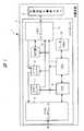
1 is a block diagram of a storage device according to
本実施の形態1において、記憶装置(半導体集積回路装置)1は、図1に示すように、フラッシュメモリに例示される電気的にデータの書き換え、消去が可能な不揮発性半導体メモリ2、およびコントローラ3から構成されている。 In the first embodiment, a storage device (semiconductor integrated circuit device) 1 includes a
このコントローラ3は、ホストインタフェース4、CPU5、CUI(Command User Interface)6、ライトバッファ7、リードバッファ8、ECC部9、ワークメモリ10、およびメモリインタフェース11などから構成されている。 The
コントローラ3は、不揮発性半導体メモリ2の制御を司り、該不揮発性半導体メモリ2に格納されたプログラムやデータなどを読み出してホスト機器へ出力し、またはホスト機器から入力されたプログラムやデータの書き込み動作指示を行う。 The
ホストインタフェース4は、ホスト機器とCPU5とのインタフェースである。CPU5は、コントローラ3におけるすべての制御を司る。CUI6は、ホストからのコマンドを解釈し、CPU5を起動する。 The
ライトバッファ7は、ホストからの読み出しデータを一時的に格納する。リードバッファ8は、不揮発性半導体メモリ2からの読み出しデータを一時的に格納する。 The
ECC部9は、ECC(Error Chek and Correction)コードの生成、ならびに不揮発性半導体メモリ2に書き込み/読み出しされるデータのECCエラーチェックと訂正を行う。 The
ワークメモリ10は、たとえば、RAMなどの半導体メモリからなり、CPU5のワーク領域のメモリとして用いられる。メモリインタフェース11は、CPU5と不揮発性半導体メモリ2とのインタフェースである。 The
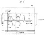
図2は、不揮発性半導体メモリ2におけるメモリアレイ(記憶領域)MAの一例を示した説明図である。 FIG. 2 is an explanatory diagram showing an example of a memory array (storage area) MA in the
図示するように、メモリアレイMAは、グローバルビット線GBLに複数のサブビット線SBLが選択用トランジスタTrを介して接続されるアレイ構造からなり、それらサブビット線SBLに、不揮発性メモリセルSがそれぞれ接続された構成からなる。 As shown in the figure, the memory array MA has an array structure in which a plurality of sub bit lines SBL are connected to a global bit line GBL via a selection transistor Tr, and a nonvolatile memory cell S is connected to each of the sub bit lines SBL. It consists of made.
サブデータ線SBLには、256本のワード線WL分の不揮発性メモリセルSが接続されており、この単位を1ストリングという。 Non-volatile memory cells S for 256 word lines WL are connected to the sub data line SBL, and this unit is called one string.
図3は、不揮発性半導体メモリ2のメモリアレイMAにおけるメモリ領域の構成例を示す説明図である。 FIG. 3 is an explanatory diagram showing a configuration example of the memory area in the memory array MA of the
メモリアレイMAは、たとえば、4つのバンクBank0〜Bank3に分割された4バンク構成からなる。バンクBank0〜Bank3には、データ格納領域DSA、およびプログラム格納領域PSA、およびテーブルブロックTBから構成されている。 The memory array MA has, for example, a four-bank configuration divided into four banks Bank0 to Bank3. The banks Bank0 to Bank3 are composed of a data storage area DSA, a program storage area PSA, and a table block TB.
データ格納領域DSAは、データが格納される領域であり、プログラム格納領域PSAは、プログラムが格納される領域である。また、テーブルブロックTBは、プログラム格納領域PSAにおけるアドレス変換テーブルが格納される領域である。 The data storage area DSA is an area where data is stored, and the program storage area PSA is an area where programs are stored. The table block TB is an area for storing an address conversion table in the program storage area PSA.
データ格納領域DSA、プログラム格納領域PSA、およびテーブルブロックTBにおいて、管理部(図3のハッチングで示した部分)KがセクタSc毎にそれぞれ備えられている。ここで、セクタScは、データ格納最小単位であり、16セクタ(4バンク列×4行)で1つのブロック(消去の最小単位)Bを構成する。 In the data storage area DSA, the program storage area PSA, and the table block TB, a management unit (a portion indicated by hatching in FIG. 3) K is provided for each sector Sc. Here, the sector Sc is a minimum data storage unit, and one block (minimum unit of erasure) B is composed of 16 sectors (4 bank columns × 4 rows).
管理部Kには、各々のブロックの管理情報が格納されている。この管理情報は、同じ行のセクタでは、バンクが異なっていても同じものが格納されており、行が異なると管理情報の内容が異なる。 The management unit K stores management information for each block. The same management information is stored in the same row sector even if the banks are different, and the content of the management information is different for different rows.
プログラム格納領域PSAの領域は任意に設定され、該プログラム格納領域PSAを設定した際に、論理アドレス/物理アドレスの変換テーブルデータを格納するテーブルブロックTBが準備されることになる。ここで、テーブルブロックTBのアドレスは、予め指定したアドレスでもよいし、簡単に検索することが可能なアドレスとしてもよい。 The area of the program storage area PSA is arbitrarily set, and when the program storage area PSA is set, a table block TB for storing logical / physical address conversion table data is prepared. Here, the address of the table block TB may be a predesignated address or an address that can be easily searched.
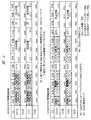
図4は、管理部Kにおける管理情報のデータ定義例を示した説明図である。 FIG. 4 is an explanatory diagram showing a data definition example of management information in the management unit K.
この図4においては、プログラム格納領域PSAの処理に関係している管理部のみを記載しており、上方に4行目のセクタの管理部を、その下方に1行目のセクタの管理部をそれぞれ示している。 In FIG. 4, only the management unit related to the processing of the program storage area PSA is described, and the sector management unit in the fourth row is shown above, and the sector management unit in the first row is shown below. Each is shown.
図示するように、4行目のセクタの管理部には、テーブルブロックのアドレスを格納する領域が備えられている。ただし、テーブルブロックのアドレスが実際に書き込まれているのは、最下位アドレスの良ブロックだけである。 As shown in the figure, the sector management section of the fourth row is provided with an area for storing the address of the table block. However, the address of the table block is actually written only in the good block at the lowest address.
その他のブロックにおける4行目のセクタの管理部のテーブルブロックアドレスを書き込む領域は消去状態(’FFh’)となっている。つまり、テーブルブロックとして使用されるブロックを検索するには、最下位アドレスの良ブロックの4行目のセクタの管理部を読み出せばよいことになる。 The area for writing the table block address of the management section of the sector in the fourth row in the other blocks is in the erased state ('FFh'). That is, in order to search for a block used as a table block, it is only necessary to read the management section of the sector in the fourth row of the good block at the lowest address.
テーブルブロックとして選択されたブロックには、1行目のセクタの管理部にコード’71h’を書き込むことでテーブル用のブロックとして認識される。また、1行目のセクタの管理部には、プログラム格納領域PSAの領域サイズ、プログラム格納領域PSAのロック判定ビットなども格納される。 A block selected as a table block is recognized as a table block by writing a code “71h” in the management section of the sector in the first row. In the sector management section in the first row, the area size of the program storage area PSA, the lock determination bit of the program storage area PSA, and the like are also stored.
図5は、不揮発性半導体メモリ2のメモリアレイMAにプログラム格納領域PSAを設定する際の状態遷移を示す説明図である。 FIG. 5 is an explanatory diagram showing a state transition when the program storage area PSA is set in the memory array MA of the
プログラム格納領域PSAは、たとえば、プログラム格納領域PSAの領域を設定するPSA設定コマンドの入力によって設定される。不揮発性半導体メモリ2は、保護制御信号(Protect Control Enable)PCEが入力される制御ピンが備えられている。 The program storage area PSA is set, for example, by inputting a PSA setting command for setting the area of the program storage area PSA. The
そして、その制御ピンに、たとえば、Hiレベルの保護制御信号PCEが入力された際に、PSA設定コマンドを受け付け、該保護制御信号PCEがLowレベルの場合には、PSA設定コマンドを受け付けない。 For example, when a Hi-level protection control signal PCE is input to the control pin, a PSA setting command is accepted, and when the protection control signal PCE is at a Low level, no PSA setting command is accepted.
メモリアレイMAは、図示するように、PSA設定前の状態(状態J1)、PSAフォーマット状態(状態J2)、およびPSAロック状態(状態J3)の3つの状態が存在する。 As shown in the figure, the memory array MA has three states: a state before PSA setting (state J1), a PSA format state (state J2), and a PSA lock state (state J3).
PSA設定前の状態(状態J1)は、PSA設定コマンドによってプログラム格納領域PSAの領域設定がされていない状態であり、消去/書き込みが可能な状態となっている(全領域がDSA領域)。PSAフォーマット状態(状態J2)は、PSA設定コマンドによってプログラム格納領域PSAの領域設定がなされた状態である。この状態J2でも、データ保護は無効であり、消去/書き込みが可能な状態となっている(PSA設定されるが動作は全領域DSA領域)。 The state before the PSA setting (state J1) is a state in which the area for the program storage area PSA is not set by the PSA setting command, and is in an erasable / writeable state (all areas are DSA areas). The PSA format state (state J2) is a state where the program storage area PSA is set by the PSA setting command. Even in this state J2, data protection is invalid and erasing / writing is possible (PSA is set, but the operation is the entire area DSA area).
PSAロック状態(状態J3)は、設定されたプログラム格納領域PSAにロック(PSAロック)がかかり、データ保護が有効になった状態であり、プログラム格納領域PSAにおいて消去/書き込みが不可となる(PSA設定された領域がPSA領域として動作)。 The PSA lock state (state J3) is a state in which the set program storage area PSA is locked (PSA lock) and data protection is enabled, and erasing / writing is disabled in the program storage area PSA (PSA The set area operates as the PSA area).
状態J3では、ロックを解除(PSAアンロック)することにより、状態J2に遷移することができる。また、状態J2,J3においては、プログラム格納領域PSAの設定を解除(PSAアンフォーマット)することにより、状態J1の状態に遷移させることができる。 In the state J3, the state can be changed to the state J2 by releasing the lock (PSA unlock). In the states J2 and J3, the state of the program storage area PSA can be canceled (PSA unformatted) to transition to the state J1.
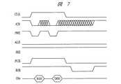
図6は、プログラム格納領域PSAの領域設定を行う際の信号サイクルを示すタイミングチャートである。 FIG. 6 is a timing chart showing a signal cycle when setting the program storage area PSA.
図6において、上方から下方にかけて、コマンドラッチイネーブルCLE、チップイネーブル/CE、ライトイネーブル/WE、アドレスラッチイネーブルALE、リードイネーブル/RE、保護制御信号PCE、レディビジーR/B、および入力されるコマンドであるデータDinをそれぞれ示している。なお、これらの各制御信号において、スラッシュ(/)を付している各記号は反転信号である。 In FIG. 6, from the top to the bottom, command latch enable CLE, chip enable / CE, write enable / WE, address latch enable ALE, read enable / RE, protection control signal PCE, ready busy R / B, and input commands Each data Din is shown. In each of these control signals, each symbol with a slash (/) is an inverted signal.
この場合、保護制御信号PCEがHiレベルとなった後、プログラム格納領域PSAの領域を設定するデータDinとしてコマンド’B0H’、’M’、’D0H’が順次入力される。 In this case, after the protection control signal PCE becomes Hi level, commands 'B0H', 'M', and 'D0H' are sequentially input as data Din for setting the program storage area PSA.
コマンド’M’が、指定領域を設定するものであり、プログラム格納領域PSAの領域設定は、たとえば、ストリング単位であり、ストリングの個数を入力する。そして、プログラム格納領域PSAの領域設定を行うコマンドが入力された後、プログラム格納領域PSAの領域設定が完了するまで、レディビジーR/Bは、ビジー(busy)となる。 The command 'M' sets the designated area, and the area setting of the program storage area PSA is, for example, in units of strings, and the number of strings is input. Then, after the command for setting the area of the program storage area PSA is input, the ready busy R / B is busy until the area setting of the program storage area PSA is completed.
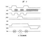
図7は、プログラム格納領域PSAの領域設定後におけるPSAロック状態の信号サイクルを示すタイミングチャートである。なお、この図7も含め、以下に示す図8、図9において、上方から下方にかけて示す信号は同一である。 FIG. 7 is a timing chart showing signal cycles in the PSA lock state after setting the program storage area PSA. In addition, in FIG. 8, FIG. 9 shown below including this FIG. 7, the signal shown from the top to the bottom is the same.
図7において、保護制御信号PCEがHiレベルとなった後、設定されたプログラム格納領域PSAのデータ保護を有効とするロックを行うデータDinとしてコマンド’B1H’、’D0H’が順次入力される。 In FIG. 7, after the protection control signal PCE becomes Hi level, commands 'B1H' and 'D0H' are sequentially input as data Din for performing locking for enabling data protection of the set program storage area PSA.
ここでも、PSAロック状態を設定するコマンドが入力された後、プログラム格納領域PSAのロック設定が完了するまで、レディビジーR/Bは、ビジー(busy)となる。 Again, after the command for setting the PSA lock state is input, the ready / busy R / B is busy until the lock setting of the program storage area PSA is completed.
図8は、PSAアンフォーマットを行う際の信号サイクルを示すタイミングチャートである。 FIG. 8 is a timing chart showing a signal cycle when PSA unformatting is performed.
PSAアンフォーマットを行う場合のコマンドは、’BFH’、’D0H’であり、図6、図7と同様に、PSAアンフォーマットを行うコマンドが入力された後、PSAアンフォーマットが完了するまで、レディビジーR/Bは、ビジー(busy)となる。 The commands for performing the PSA unformat are 'BFH' and 'D0H'. As in FIG. 6 and FIG. 7, after the command for performing the PSA unformat is input, the ready busy is completed until the PSA unformat is completed. R / B becomes busy.
図9は、PSAアンロックを行う際の信号サイクルを示すタイミングチャートである。 FIG. 9 is a timing chart showing a signal cycle when performing PSA unlocking.
PSAアンロックを行う場合のコマンドは、’BEH’、’D0H’となる。そして、図6〜図8と同様に、PSAアンロックを行うコマンドが入力された後、PSAアンロックが完了するまで、レディビジーR/Bは、ビジー(busy)となる。 Commands for performing PSA unlock are 'BEH' and 'D0H'. 6 to 8, the ready busy R / B is busy until the PSA unlock is completed after the command for performing the PSA unlock is input.
図10は、記憶装置1におけるPSAフォーマットの処理例を示すフローチャートである。 FIG. 10 is a flowchart illustrating a processing example of the PSA format in the
まず、メモリアレイMAにおいて、プログラム格納領域PSAの領域が設定されているか否かを判定する(ステップS101)。このステップS101の処理において、プログラム格納領域PSAの領域が設定されている(PSAフォーマット済み)場合には、PSAフォーマット処理を終了する。 First, it is determined whether or not an area for the program storage area PSA is set in the memory array MA (step S101). If the program storage area PSA area is set (PSA formatted) in the process of step S101, the PSA formatting process is terminated.
また、ステップS101の処理において、PSAフォーマット済みでない場合、テーブルブロックとして使用するブロックを検索し(ステップS102)、管理部にテーブルブロックであることを示すコード、ならびにその領域サイズを書き込む(ステップS103)。 If the PSA format is not completed in the process of step S101, a block to be used as a table block is searched (step S102), and a code indicating the table block and its area size are written in the management unit (step S103). .
続いて、検索したテーブルブロックのアドレス情報を、たとえば、最下位アドレスの良ブロックの管理部などの予め設定した位置に書き込みを行う(ステップS104)。 Subsequently, the address information of the searched table block is written in a preset position such as a management unit of the good block having the lowest address (step S104).
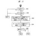
図11は、記憶装置1におけるPSAロックの処理例を示すフローチャートである。 FIG. 11 is a flowchart illustrating an example of PSA lock processing in the
まず、プログラム格納領域PSAがフォーマット済みであるか否かを判定し(ステップS201)、未フォーマットであるなら処理を終了する。ステップS201の処理で、フォーマット済みである場合には、プログラム格納領域PSAがロックされているか否かを判定し(ステップS202)、ロック済みの場合には、処理が終了となる。 First, it is determined whether or not the program storage area PSA has been formatted (step S201), and if it has not been formatted, the process ends. If it has been formatted in the process of step S201, it is determined whether or not the program storage area PSA is locked (step S202). If it has been locked, the process ends.
続いて、プログラム格納領域PSAの論理アドレスと物理アドレスとの対応付けを行い、論理アドレスから、不揮発性半導体メモリ2の物理アドレスへの変換を管理するアドレス変換テーブルを生成する(ステップS203)。 Subsequently, the logical address and the physical address of the program storage area PSA are associated with each other, and an address conversion table for managing conversion from the logical address to the physical address of the
そして、テーブルブロックに生成したアドレス変換テーブルの書き込みを行う(ステップS204)。このとき、テーブルブロックの管理部には、PSAロック判定ビットの書き込みも行われる。 Then, the generated address conversion table is written in the table block (step S204). At this time, the PSA lock determination bit is also written in the management unit of the table block.
その後、書き込みが完了したか否かの判断を行い(ステップS205)。完了した場合には処理が終了となり、書き込みに失敗した場合には、新たなテーブルブロックを設け、テーブルデータの書き込みを行う。 Thereafter, it is determined whether or not the writing is completed (step S205). If completed, the process ends. If writing fails, a new table block is provided and table data is written.
図12は、記憶装置1におけるPSAアンロックの処理例を示すフローチャートである。 FIG. 12 is a flowchart illustrating an example of PSA unlock processing in the
まず、プログラム格納領域PSAがフォーマット済みであるか否かを判定し(ステップS301)する。プログラム格納領域PSAがフォーマット済みの場合には、プログラム格納領域PSAがロックされているかを判定する(ステップS302)。 First, it is determined whether or not the program storage area PSA has been formatted (step S301). If the program storage area PSA has been formatted, it is determined whether the program storage area PSA is locked (step S302).
ステップS301の処理において、プログラム格納領域PSAがフォーマットされていない場合、およびステップS302の処理でプログラム格納領域PSAがロックされていない場合には、処理を終了する。 In the process of step S301, if the program storage area PSA is not formatted and if the program storage area PSA is not locked in the process of step S302, the process ends.
また、ステップS302の処理において、プログラム格納領域PSAがロックされている場合には、テーブルブロックに格納されているデータを消去する(ステップS303)。この場合、管理部には、テーブルブロックを示すコード、およびプログラム格納領域PSAの領域サイズのデータがかかれた状態であり、ロック判定ビットが消去される。これにより、PSAフォーマット状態に戻されることになる。 If the program storage area PSA is locked in the process of step S302, the data stored in the table block is deleted (step S303). In this case, the code indicating the table block and the area size data of the program storage area PSA are written in the management unit, and the lock determination bit is erased. As a result, the PSA format state is restored.
図13は、記憶装置1におけるPSAアンフォーマットの処理例を示すフローチャートである。 FIG. 13 is a flowchart illustrating an example of PSA unformat processing in the
まず、プログラム格納領域PSAがフォーマット済みであるか否かを判定し(ステップS401)、該プログラム格納領域PSAが未フォーマットの場合には、処理が終了となる。 First, it is determined whether or not the program storage area PSA has been formatted (step S401). If the program storage area PSA has not been formatted, the process ends.
プログラム格納領域PSAがフォーマット済みの場合、テーブルブロックの検索を行い(ステップS402)、検索したテーブルブロックの登録を解消する(ステップS403)。 If the program storage area PSA has been formatted, the table block is searched (step S402), and the registration of the searched table block is canceled (step S403).
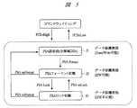
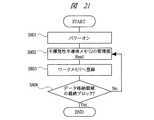
図14は、記憶装置1のプログラム格納領域PSAの領域設定時におけるパワーオンリセット(初期化動作)の処理例とプログラム格納領域PSAの状態とを示すフローチャートである。 FIG. 14 is a flowchart showing a processing example of power-on reset (initialization operation) and the state of the program storage area PSA when the area of the program storage area PSA of the
図14において、左側は、プログラム格納領域PSAの領域設定時におけるパワーオンリセットの処理フローを示しており、右側は、プログラム格納領域PSAの領域設定時におけるプログラム格納領域PSAの領域の状態を示している。 In FIG. 14, the left side shows the processing flow of power-on reset when setting the area of the program storage area PSA, and the right side shows the state of the area of the program storage area PSA when setting the area of the program storage area PSA. Yes.
まず、パワーオンによって、リセット信号が入力される(ステップS501)。PSAロックが設定されている場合には、テーブルブロックのアドレス変換テーブルの読み出しを行い(ステップS502)、レディ状態となる(ステップS503)。 First, a reset signal is input by power-on (step S501). If the PSA lock is set, the address conversion table of the table block is read (step S502), and the ready state is entered (step S503).
このステップS503の処理後、プログラム格納領域PSAはリードが可能となる。一方、データ格納領域DSAは、アクセスが不可の状態となっている。 After the processing in step S503, the program storage area PSA can be read. On the other hand, the data storage area DSA is in an inaccessible state.
そして、データ格納領域DSAのイニシャライズ動作を行うことで(ステップS504)、データ格納領域DSAのアドレス変換テーブルが生成される。 Then, by performing an initialization operation for the data storage area DSA (step S504), an address conversion table for the data storage area DSA is generated.
それによって、不揮発性半導体メモリ2はレディ状態となり、プログラム格納領域PSAのリードが可能であるとともに、データ格納領域DSAのアクセスが可能な状態となる。 As a result, the
また、プログラム格納領域PSAのロックが設定されていない場合(PSAフォーマット、またはPSAアンフォーマット)には、データ格納領域DSAのイニシャライズ動作を行い(ステップS505)、すべてのセクタの管理部をリードし、アドレス変換テーブルを作成する。ステップS505が終了すると、不揮発性半導体メモリ2はレディ状態となり、データ格納領域DSAのアクセスが可能な状態となる。 If the lock of the program storage area PSA is not set (PSA format or PSA unformat), the data storage area DSA is initialized (step S505), and the management units of all sectors are read. Create an address translation table. When step S505 ends, the
図15は、データ格納領域DSAのイニシャライズの処理例を示すフローチャートである。 FIG. 15 is a flowchart showing an example of a process for initializing the data storage area DSA.
まず、ロックされていないプログラム格納領域PSA、およびデータ格納領域DSAにおけるすべての管理部のリードを行う(ステップS601)。その後、データ格納領域DSAのアドレス変換テーブルを生成し(ステップS602)、生成したアドレス変換テーブルをワークメモリ10に格納する。 First, all management units in the unlocked program storage area PSA and data storage area DSA are read (step S601). Thereafter, an address conversion table of the data storage area DSA is generated (step S602), and the generated address conversion table is stored in the
図16は、記憶装置1を用いて構成した電子システムの一例を示したブロック図である。 FIG. 16 is a block diagram illustrating an example of an electronic system configured using the
図示するように、記憶装置1は、たとえば、ホスト機器のプロセッサPr、およびキャッシュメモリChとバスBを介して相互接続される。記憶装置1の不揮発性半導体メモリ2には、たとえば、ホスト用のプログラムやデータが格納されており、パワーオン時には、該ホスト用のプログラムが不揮発性半導体メモリ2から読み出され、たとえば、SRAM(Static Random Access Memory)/SDRAM(Synchronous Dynamic RAM)などからなるキャッシュメモリChに転送される。 As shown in the figure, the
よって、パワーオン時には、プログラムを格納するプログラム格納領域PSAのみのアクセスが可能になればよく、データ格納領域DSAのイニシャライズを電子システムのプロセッサPrの初期化時などのバックグラウンドで行うことが可能となる。 Therefore, at the time of power-on, it is sufficient that only the program storage area PSA for storing the program can be accessed, and the data storage area DSA can be initialized in the background such as when the processor Pr of the electronic system is initialized. Become.
それにより、本実施の形態1によれば、記憶装置1におけるパワーオンリセットの処理時間を大幅に短縮することができる。 Thereby, according to the first embodiment, the processing time of the power-on reset in the
(実施の形態2)
図17は、本発明の実施の形態2による記憶装置のパワーオンリセット時のアドレス変換テーブルの生成例を示す説明図、図18は、図17のパワーオン時に生成されるアドレス変換テーブルの処理例を示すフローチャート、図19は、図18アドレス変換テーブルの生成後に生成されるアドレステーブルの処理例を示すフローチャートである。(Embodiment 2)
FIG. 17 is an explanatory diagram illustrating an example of generation of an address conversion table at the time of power-on reset of the storage device according to the second embodiment of the present invention, and FIG. FIG. 19 is a flowchart showing a processing example of the address table generated after the generation of the address conversion table in FIG.
本実施の形態2において、記憶装置1は、前記実施の形態1の図1と同じであり、不揮発性半導体メモリ2、およびコントローラ3から構成されており、該コントローラ3は、ホストインタフェース4、CPU5、CUI6、ライトバッファ7、リードバッファ8、ECC部9、ワークメモリ10、およびメモリインタフェース11から構成されている。 In the second embodiment, the
図17は、記憶装置1のパワーオン時に生成されるアドレス変換テーブルの生成例を示したものである。 FIG. 17 shows an example of generating an address conversion table generated when the
この場合、図示するように、不揮発性半導体メモリ2のデータ格納領域DSAは、2つのデータ格納領域DSA1,DSA2に任意に分割されている。そして、記憶装置1のパワーオンリセット処理時には、データ格納領域DSA1のアドレス変換テーブルのみが生成される。これらデータ格納領域DSA1,DSA2の領域設定は、たとえば、ホスト機器からの設定コマンドの入力によって設定される。 In this case, as shown in the figure, the data storage area DSA of the
そして、データ格納領域DSA1のアドレス変換テーブルの生成が終了し、ホスト機器からデータ格納領域DSA2のアドレス変換テーブルを生成するコマンドが出力されると、そのコマンドを受けて、データ格納領域DSA2のアドレス変換テーブルが生成される。 When the generation of the address conversion table of the data storage area DSA1 is completed and a command for generating the address conversion table of the data storage area DSA2 is output from the host device, the address conversion of the data storage area DSA2 is received in response to the command. A table is generated.
次に、データ格納領域DSA1におけるアドレス変換テーブルの生成例を、図18のフローチャートを用いて説明する。なお、この図18に示す処理は、図14のステップS504の処理において行われるものである。 Next, an example of generating an address conversion table in the data storage area DSA1 will be described with reference to the flowchart of FIG. The process shown in FIG. 18 is performed in the process of step S504 in FIG.
まず、パワーオンによってリセット信号が入力される(ステップS601)、図14のステップS503の処理が終了すると、データ格納領域DSA1の管理部をリードし(ステップS602)、該データ格納領域DSA1における先頭ブロックのアドレス変換テーブルを作成する。 First, a reset signal is input by power-on (step S601). When the processing of step S503 in FIG. 14 is completed, the management unit of the data storage area DSA1 is read (step S602), and the first block in the data storage area DSA1 Create an address translation table.
作成されたアドレス変換テーブルは、ワークメモリ10に格納される(ステップS603)。そして、データ格納領域DSA1における最終ブロックのアドレス変換テーブルが生成されるまでステップS602,S603の処理を繰り返す(ステップSS604)。データ格納領域DSA1のすべてのアドレス変換テーブルが生成されると、データ格納領域DSA1におけるアドレス変換テーブルの生成処理が終了となる。 The created address conversion table is stored in the work memory 10 (step S603). The processes in steps S602 and S603 are repeated until the address conversion table for the final block in the data storage area DSA1 is generated (step SS604). When all the address conversion tables in the data storage area DSA1 are generated, the address conversion table generation process in the data storage area DSA1 is completed.
また、データ領域格納DSA2におけるアドレス変換テーブルの生成例を、図19のフローチャートを用いて説明する。 An example of generating an address conversion table in the data area storage DSA2 will be described with reference to the flowchart of FIG.
図18に示したデータ格納領域DSA1におけるアドレス変換テーブルの生成処理が終了した後、ホスト機器から、データ格納領域DSA2のアドレス変換テーブルを生成するコマンドが入力されると(ステップS701)、それを受けて、不揮発性半導体メモリ2におけるデータ格納領域DSA2の管理部をリードし(ステップS702)、該データ格納領域DSA2における先頭ブロックのアドレス変換テーブルを作成し、そのアドレス変換テーブルを、ワークメモリ10に格納する(ステップS703)。 After the generation processing of the address conversion table in the data storage area DSA1 shown in FIG. 18 is completed, a command for generating the address conversion table in the data storage area DSA2 is input from the host device (step S701). Then, the management unit of the data storage area DSA2 in the
そして、データ格納領域DSA2の最終ブロックのアドレス変換テーブルが生成されるまでステップS702,S703の処理を繰り返し行う(ステップS704)。データ格納領域DSA2のすべてのブロックのアドレス変換テーブルが生成されると、データ格納領域DSA2におけるアドレス変換テーブルの生成処理が終了となる。 Then, the processes in steps S702 and S703 are repeated until the address conversion table for the last block in the data storage area DSA2 is generated (step S704). When the address conversion tables for all the blocks in the data storage area DSA2 are generated, the address conversion table generation process in the data storage area DSA2 ends.
それにより、本実施の形態2おいても、記憶装置1におけるパワーオンリセットの処理時間を大幅に短縮することができる。 Thereby, also in the second embodiment, the processing time of the power-on reset in the
また、本実施の形態2では、不揮発性半導体メモリ2のメモリ領域を任意の2つのデータ格納領域DSA1,DSA2に分割するものとしたが、たとえば、記憶装置1が複数の不揮発性半導体メモリを備える場合には、パワーオン時にアドレス変換テーブルが生成する不揮発性半導体メモリと、ホスト機器からのコマンド入力後にアドレス変換テーブルを生成する不揮発性半導体メモリとを予め設定しておくようにしてもよい。 In the second embodiment, the memory area of the
図20は、たとえば、2つの不揮発性半導体メモリを備えた記憶装置におけるパワーオン時に生成されるアドレス変換テーブルの生成例を示したものである。 FIG. 20 shows an example of generating an address conversion table generated at power-on in a storage device including two nonvolatile semiconductor memories, for example.
この場合、図示するように、パワーオンリセット処理時に、予め設定された一方の不揮発性半導体メモリ2のデータ格納領域DSAのアドレス変換テーブルが生成される。その後、ホスト機器からアドレス変換テーブルを生成するコマンドが出力されると、他方の不揮発性半導体メモリ2aにおけるデータ格納領域DSAのアドレス変換テーブルが生成される。 In this case, as illustrated, an address conversion table of the data storage area DSA of one of the
よって、ワークメモリ10には、図20の右側に示すような、不揮発性半導体メモリ22aのアドレス変換テーブルが生成される。 Therefore, an address conversion table of the nonvolatile semiconductor memory 22a as shown on the right side of FIG. 20 is generated in the
図21は、2つの不揮発性半導体メモリ2,2aを備えた記憶装置におけるパワーオン時に生成されるアドレス変換テーブルの生成例を示したフローチャートである。 FIG. 21 is a flowchart showing an example of generating an address conversion table generated at power-on in a storage device including two
まず、パワーオンによって(ステップS801)リセット信号が入力され、図14のステップS503の処理が終了すると、不揮発性半導体メモリ2のデータ格納領域DSAにおける管理部をリードし(ステップS802)、該不揮発性半導体メモリ2における先頭ブロックのアドレス変換テーブルを作成する。 First, when a reset signal is input by power-on (step S801) and the processing of step S503 in FIG. 14 is completed, the management unit in the data storage area DSA of the
作成されたアドレス変換テーブルは、ワークメモリ10に格納される(ステップS803)。そして、不揮発性半導体メモリ2におけるすべてのブロックのアドレス変換テーブルが生成されるまでステップS802,S803の処理を繰り返す(ステップS804)。 The created address conversion table is stored in the work memory 10 (step S803). Then, the processes in steps S802 and S803 are repeated until the address conversion tables for all the blocks in the
不揮発性半導体メモリ2におけるすべてブロックのアドレス変換テーブルが生成されると、アドレス変換テーブルの生成処理が終了となる。 When the address conversion table for all blocks in the
また、他方の不揮発性半導体メモリ2aにおけるアドレス変換テーブルの生成例を、図22のフローチャートを用いて説明する。 An example of generating an address conversion table in the other
図21に示したアドレス変換テーブルの生成処理が終了した後、ホスト機器から、不揮発性半導体メモリ2aのアドレス変換テーブルを生成するコマンドが入力されると(ステップS901)、それを受けて、不揮発性半導体メモリ2aにおけるデータ格納領域DSAの管理部をリードし(ステップS902)、該不揮発性半導体メモリ2aにおける先頭ブロックのアドレス変換テーブルを作成し、そのアドレス変換テーブルをワークメモリ10に格納する(ステップS903)。 After the generation processing of the address conversion table shown in FIG. 21 is completed, when a command for generating the address conversion table of the
他方の不揮発性半導体メモリの最終ブロックのアドレス変換テーブルが生成されるまでステップS902,S903の処理を繰り返す(ステップS904)。そして、他方の不揮発性半導体メモリのすべてのアドレス変換テーブルが生成されると、アドレス変換テーブルの生成処理が終了となる。 The processes in steps S902 and S903 are repeated until the address conversion table for the final block of the other nonvolatile semiconductor memory is generated (step S904). When all the address conversion tables of the other nonvolatile semiconductor memory are generated, the generation process of the address conversion table ends.
それにより、複数の不揮発性半導体メモリを備えた記憶装置であっても、該記憶装置におけるパワーオンリセットの処理時間を大幅に短縮することができる。 Thereby, even in a storage device including a plurality of nonvolatile semiconductor memories, the processing time for power-on reset in the storage device can be significantly reduced.
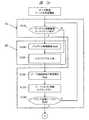
(実施の形態3)
図23は、本発明の実施の形態3による記憶装置のパワーオンリセット処理を示したフローチャート、図24は、図23に示すステップS1002,S1003の処理の詳細なフローチャート、図25は、図24の処理における記憶装置の信号タイミングチャートである。(Embodiment 3)
FIG. 23 is a flowchart showing power-on reset processing of the storage device according to the third embodiment of the present invention, FIG. 24 is a detailed flowchart of processing in steps S1002 and S1003 shown in FIG. 23, and FIG. It is a signal timing chart of the storage device in processing.
本実施の形態3でも、記憶装置1は、前記実施の形態1の図1と同じであり、不揮発性半導体メモリ2、およびコントローラ3から構成されており、該コントローラ3は、ホストインタフェース4、CPU5、CUI6、ライトバッファ7、リードバッファ8、ECC部9、ワークメモリ10、およびメモリインタフェース11から構成されている。 Also in the third embodiment, the
本実施の形態3において、コントローラ3は、データ格納領域DSAにおけるアドレス変換テーブルの生成中に、プログラム格納領域PSAのリードコマンドを受け付ける機能を有している。 In the third embodiment, the
次に、記憶装置1によるパワーオンリセット処理について、図23のフローチャートを用いて説明する。 Next, power-on reset processing by the
まず、電源が投入され、不揮発性半導体メモリ2の処理化が終了する(ステップS1001)。このステップS1001の処理では、図23の右上側に示すように、プログラム格納領域PSAのアドレス変換テーブルが生成される。 First, the power is turned on, and the processing of the
その後、ホスト機器から、データ格納領域DSAのアドレス変換テーブルを生成するコマンドが投入された後(ステップS1002)、プログラム格納領域PSAのプログラムがワークメモリ10に展開される(ステップS1003)。 Thereafter, after a command for generating an address conversion table of the data storage area DSA is input from the host device (step S1002), the program in the program storage area PSA is expanded in the work memory 10 (step S1003).
このステップS1002,S1003の処理では、図23の右上側に示すように、データ格納領域DSAのアドレス変換テーブルが生成され、ステップS1003の処理では、プログラム格納領域PSAのプログラムが読み出される。また、ステップS1003の処理では、点線で囲んだ範囲に示すように、データ格納領域DSAのアドレス変換テーブルの生成がプログラム格納領域PSAからのプログラムの読み出しのバックグランドで行われるように処理される。 In the processing of steps S1002 and S1003, as shown in the upper right side of FIG. 23, the address conversion table of the data storage area DSA is generated, and in the processing of step S1003, the program in the program storage area PSA is read. Further, in the process of step S1003, as shown in the range surrounded by the dotted line, the generation of the address conversion table of the data storage area DSA is performed in the background of reading the program from the program storage area PSA.
そして、ワークメモリ10に展開されたプログラムによる記憶装置1の初期化動作が行われて(ステップS1004)、初期化が終了となる。 Then, the initialization operation of the
続いて、図23のステップS1002,S1003の処理について、図24のフローチャート、ならびに図25のタイミングチャートを用いて詳しく説明する。 Next, the processing in steps S1002 and S1003 in FIG. 23 will be described in detail with reference to the flowchart in FIG. 24 and the timing chart in FIG.
図24においては、上方から下方にかけて、ホスト機器から出力されるコマンド、ホスト機器から出力されるデータ読み出し用のクロック信号CLK、およびコントローラ3から出力されるレディ/ビジーR/B、およびコントローラ3の内部動作状態、割り込みリクエスト信号のタイミングをそれぞれ示している。 24, from the top to the bottom, the command output from the host device, the data read clock signal CLK output from the host device, the ready / busy R / B output from the
まず、ホスト機器から、データ格納領域DSAにおけるアドレス変換テーブルを生成するコマンドを受けると、記憶装置1は、図24の(A)に示すルーチン処理を開始し、プログラム格納領域リードコマンドが発行されたか否かを判断する(ステップS1101)。 First, when a command for generating an address conversion table in the data storage area DSA is received from the host device, the
ステップS1001の処理において、プログラム格納領域リードコマンドが発行されていない場合、コントローラ3は、ホスト機器からはバックグランド動作として見なせるようにレディビジーR/Bを’Hi’としてレディ(Ready)状態とし、データ格納領域DSAの管理部のデータを読み出し(ステップS1102)、1ブロック分のアドレス変換テーブルを作成してワークメモリ10に格納する(ステップS1103)。 If the program storage area read command has not been issued in the process of step S1001, the
続いて、ステップS1101の処理に戻り、プログラム格納領域リードコマンドがステップS1102,S1103の処理中に発行されたか否かを判断する。 Subsequently, the processing returns to step S1101, and it is determined whether a program storage area read command has been issued during the processing of steps S1102 and S1103.
ホスト機器からプログラム格納領域リードコマンドが発行されている場合、コントローラ3内部では、割り込みリクエスト信号のフラグが’Hi’となる。このとき、コントローラ3は、レディビジーR/Bをビジーとして図24の(B)に示すルーチン処理を割り込ませ、割り込みリクエスト信号のフラグをリセット(’Lo’)する。 When a program storage area read command is issued from the host device, the flag of the interrupt request signal becomes “Hi” in the
続いて、コントローラ3は、プログラム格納領域PSAのデータを読み出す(ステップS1104)。そして、読み出しデータのエラー訂正が終了し、セカンドアクセスが可能な状態になると(ステップS1105)、再びレディ/ビジーR/Bをレディとし、ホスト機器からのセカンドアクセス用のコマンドを受け付けられる状態にする。
(B)のルーチン処理が終了すると、ステップS1102,S1103の処理を行う。(A)のルーチン処理は、データ格納領域DSAにおけるアドレス変換テーブルが完成するまで行われる(ステップS1106)。Subsequently, the
When the routine process (B) ends, the processes of steps S1102 and S1103 are performed. The routine process (A) is performed until the address conversion table in the data storage area DSA is completed (step S1106).
このとき、ホスト機器からセカンドアクセス用のコマンドが発行されると、コントローラ3は、アドレス変換テーブルを生成する(A)のルーチン処理を行いながら、ホスト機器からのデータ読み出し用のクロック信号CLKに基づいて、読み出しデータをホスト機器に転送する。 At this time, when a command for second access is issued from the host device, the
プログラム格納領域PSAのデータの読み出し動作は、データ格納領域DSAからのデータ読み出しと同様に、ファーストアクセス、およびセカンドアクセスからなる。ファーストアクセスでは、コントローラ3によって不揮発性半導体メモリ2から読み出したデータがリードバッファ8まで転送される。 The data read operation of the program storage area PSA includes first access and second access in the same manner as data read from the data storage area DSA. In the first access, data read from the
そして、セカンドアクセスでは、リードバッファ8に格納されたデータがクロック信号CLKによってホストへ読み出される。このセカンドアクセスの間、コントローラ3は、読み出し動作としてはフリーの状態であり、他の内部動作を行うことが可能な状態となる。 In the second access, the data stored in the read
よって、セカンドアクセスのフリーの状態を利用してアドレス変換テーブルの生成を継続して行うことができる。 Therefore, it is possible to continuously generate the address conversion table using the second access free state.
なお、この場合、データ格納領域DSAにおけるアドレス変換テーブルの生成完了を知るために、ステータスリードコマンドを設ける。任意の回数のプログラム格納領域PSAのデータの読み出しが終了し、ホスト機器がデータ格納領域DSAにアクセスしたい場合には、該ホスト機器がステータスリードコマンドを出力し、データ格納領域DSAのアドレス変換テーブルの生成が完了したことを確認してから行われることになる。 In this case, a status read command is provided in order to know completion of generation of the address conversion table in the data storage area DSA. When reading of data in the program storage area PSA of any number of times is completed and the host device wishes to access the data storage area DSA, the host device outputs a status read command, and the address conversion table of the data storage area DSA It will be done after confirming that the generation is complete.
それにより、本実施の形態3においては、データ格納領域DSAにおけるアドレス変換テーブルの生成中にプログラム格納領域PSAのデータを読み出すことが可能となる。 Thereby, in the third embodiment, it is possible to read data in the program storage area PSA during the generation of the address conversion table in the data storage area DSA.
また、プログラム格納領域PSAのデータを読み出しながら、データ格納領域DSAにおけるアドレス変換テーブルを生成することが可能となるので、より短時間でデータ格納領域DSAへアクセスすることができる。 In addition, since the address conversion table in the data storage area DSA can be generated while reading the data in the program storage area PSA, the data storage area DSA can be accessed in a shorter time.
さらに、本実施の形態では、1つの不揮発性半導体メモリのメモリ領域をプログラム格納領域PSAとデータ格納領域DSAとに分割した場合について記載したが、たとえば、図26に示すように、記憶装置1に2つの不揮発性半導体メモリ2,2aを備え、一方の不揮発性半導体メモリ2のメモリ領域をプログラム格納領域PSAとし、他方の不揮発性半導体メモリ2aのメモリ領域をデータ格納領域DSAとするようにしてもよい。 Furthermore, in the present embodiment, the case where the memory area of one nonvolatile semiconductor memory is divided into the program storage area PSA and the data storage area DSA has been described. For example, as shown in FIG. Two
この場合、図26の記憶装置1は、不揮発性半導体メモリ2aが新たにメモリインタフェース11に接続されており、その他の接続構成は、図1に示す記憶装置1と同じとなっている。 In this case, in the
図27は、図26に示す記憶装置1におけるデータ格納領域DSAのアドレス変換テーブル生成における処理例を示すフローチャートである。 FIG. 27 is a flowchart showing a processing example in generating an address conversion table for the data storage area DSA in the
まず、ホスト機器から、データ格納領域DSAにおけるアドレス変換テーブルを生成するコマンドを受けると、コントローラ3は、プログラム格納領域リードコマンドが発行されたか否かを判断する(ステップS1201)。 First, upon receiving a command for generating an address conversion table in the data storage area DSA from the host device, the
ステップS1201の処理において、プログラム格納領域リードコマンドが発行されていない場合、コントローラ3は、不揮発性半導体メモリ2aの管理部を読み出し(ステップS1203)、生成したアドレス変換テーブルをワークメモリ10に登録する(ステップS1203)。 If the program storage area read command has not been issued in the process of step S1201, the
また、ステップS1201の処理において、プログラム格納領域リードコマンドが発行されている場合には、不揮発性半導体メモリ2aの管理部を読み出してアドレス変換テーブルを生成する処理と、プログラム格納領域PSAのデータを読み出しとを並列して行う(ステップS1204)。 If a program storage area read command has been issued in the process of step S1201, the management unit of the
続いて、読み出しデータのエラー訂正が終了し、セカンドアクセスが可能な状態になると(ステップS1205)、ステップS1203の処理を行う。これらステップS1201〜S1205の処理は、、不揮発性半導体メモリ2aのデータ格納領域DSAにおけるアドレス変換テーブルが完成するまで行われる(ステップS1206)。 Subsequently, when error correction of read data is completed and second access is possible (step S1205), the process of step S1203 is performed. The processes in steps S1201 to S1205 are performed until the address conversion table in the data storage area DSA of the
それにより、不揮発性半導体メモリ2のプログラム格納領域PSAからの読み出しと、不揮発性半導体メモリ2aにおけるデータ格納領域DSAの管理部の読み出しを並列して行うことができるので、不揮発性半導体メモリ2,2aのファーストアクセスののべ時間を短縮することができる。 Thereby, reading from the program storage area PSA of the
また、図26では、1つのCPU5によって不揮発性半導体メモリ2,2aを制御する構成としたが、2つのCPUを設け、各々のCPUでそれぞれの不揮発性半導体メモリを個別に制御する構成としてもよい。 Further, in FIG. 26, the
それにより、時分割で行われていたプログラム格納領域PSAの読み出しとデータ格納領域DSAにおけるアドレス変換テーブルの生成とを並列して処理することができるので、より動作時間を短縮することができる。 As a result, the reading of the program storage area PSA performed in a time division manner and the generation of the address conversion table in the data storage area DSA can be processed in parallel, so that the operation time can be further shortened.
以上、本発明者によってなされた発明を実施の形態に基づき具体的に説明したが、本発明は前記実施の形態に限定されるものではなく、その要旨を逸脱しない範囲で種々変更可能であることはいうまでもない。 As mentioned above, the invention made by the present inventor has been specifically described based on the embodiment. However, the present invention is not limited to the embodiment, and various modifications can be made without departing from the scope of the invention. Needless to say.
本発明は、不揮発性半導体メモリにおける初期化動作時間の短縮技術に適している。 The present invention is suitable for a technique for shortening an initialization operation time in a nonvolatile semiconductor memory.
1 記憶装置(半導体集積回路装置)
2,2a 不揮発性半導体メモリ
3 コントローラ
4 ホストインタフェース
5 CPU
6 CUI
7 ライトバッファ
8 リードバッファ
9 ECC部
10 ワークメモリ
11 メモリインタフェース
MA メモリアレイ(記憶領域)
GBL グローバルビット線
SBL サブビット線
Tr 選択用トランジスタ
S 不揮発性メモリセル
Bank0〜Bank3 バンク
DSA データ格納領域
PSA プログラム格納領域
TB テーブルブロック
K 管理部
Sc セクタ
B ブロック1. Memory device (semiconductor integrated circuit device)
2, 2a
6 CUI
7 Write
GBL global bit line SBL sub-bit line Tr selection transistor S non-volatile memory cell Bank0 to Bank3 bank DSA data storage area PSA program storage area TB table block K management section Sc sector B block
Claims (16)
Translated fromJapanese前記不揮発性半導体メモリのメモリ領域は、
データの更新が許可されない第1状態に設定された領域と、データの更新が許可される第2状態に設定された領域と、前記第1状態に設定された領域の物理アドレス毎に外部から供給される論理アドレスを対応付けしたアドレス変換テーブルを格納するテーブルブロックとを備え、
前記コントローラは、
初期化動作前に予め生成した前記第1状態に設定された領域のアドレス変換テーブルを前記テーブルブロックに格納し、
前記第2状態に設定された領域のアドレス変換テーブルは、初期化動作毎に生成することを特徴とする半導体集積回路装置。A semiconductor integrated circuit comprising a nonvolatile semiconductor memory having a plurality of nonvolatile memory cells and capable of storing predetermined information, and a controller for instructing operation of the nonvolatile semiconductor memory based on a command issued from the outside A device,
The memory area of the nonvolatile semiconductor memory is
Supplied from the outside for each physical address of the area set in the first state where data update is not permitted, the area set in the second state where data update is permitted, and the area set in the first state A table block for storing an address conversion table in which logical addresses to be associated are associated,
The controller is
Storing the address conversion table of the area set in the first state generated in advance before the initialization operation in the table block;
The semiconductor integrated circuit device, wherein the address conversion table of the area set to the second state is generated for each initialization operation.
前記第1状態に設定された領域、および前記第2状態に設定された領域は、別ストリングにそれぞれ設けられていることを特徴とする半導体集積回路装置。The semiconductor integrated circuit device according to claim 1.
The region set in the first state and the region set in the second state are provided in different strings, respectively.
前記コントローラは、
前記第1状態に設定された領域をストリング単位で任意の領域に設定することを特徴とする半導体集積回路装置。The semiconductor integrated circuit device according to claim 1 or 2,
The controller is
A semiconductor integrated circuit device, wherein the region set in the first state is set to an arbitrary region in units of strings.
前記コントローラは、
前記第1状態に設定された領域の領域設定を外部から入力されたコマンドに基づいて行うことを特徴とする半導体集積回路装置。The semiconductor integrated circuit device according to any one of claims 1 to 3,
The controller is
A semiconductor integrated circuit device comprising: setting an area set in the first state based on an externally input command.
前記コントローラは、
前記テーブルブロックに格納された前記第1状態に設定された領域のアドレス変換テーブルを読み出した際に、前記第1状態に設定された領域へのアクセスを許可することを特徴とする半導体集積回路装置。The semiconductor integrated circuit device according to any one of claims 1 to 4,
The controller is
A semiconductor integrated circuit device that permits access to an area set in the first state when an address conversion table of the area set in the first state stored in the table block is read. .
前記不揮発性半導体メモリの第2状態に設定された領域は、
第1の領域と第2の領域とに任意に分割されており、
前記コントローラは、
前記第1の領域のアドレス変換テーブルを初期化動作毎に生成し、前記第2の領域のアドレス変換テーブルを外部から入力されたコマンドに基づいて生成することを特徴とする半導体集積回路装置。The semiconductor integrated circuit device according to any one of claims 1 to 4,
The region set to the second state of the nonvolatile semiconductor memory is
It is arbitrarily divided into a first area and a second area,
The controller is
The semiconductor integrated circuit device, wherein the address conversion table of the first area is generated for each initialization operation, and the address conversion table of the second area is generated based on an externally input command.
前記コントローラは、
前記第2状態に設定された領域におけるアドレス変換テーブルの生成中に、前記第1状態に設定された領域のデータを読み出す外部から入力されるリードコマンドを受け付け、前記アドレス変換テーブルの生成と前記第1状態に設定された領域からのデータの読み出しとを時分割で行うことを特徴とする半導体集積回路装置。The semiconductor integrated circuit device according to any one of claims 1 to 4,
The controller is
During generation of the address conversion table in the area set in the second state, a read command input from the outside that reads data in the area set in the first state is received, and the generation of the address conversion table and the first A semiconductor integrated circuit device characterized in that data is read from an area set in one state in a time-sharing manner.
前記コントローラは、
外部入力されるリードコマンドを受け付けた際に、前記第1状態に設定された領域から読み出したデータを、前記不揮発性半導体メモリからの読み出しデータを一時的に格納するリードバッファから外部に転送するセカンドアクセス時に前記第2状態に設定された領域におけるアドレス変換テーブルを生成することを特徴とする半導体集積回路装置。The semiconductor integrated circuit device according to claim 7,
The controller is
A second that transfers data read from the region set to the first state to the outside from a read buffer that temporarily stores read data from the nonvolatile semiconductor memory when an externally input read command is received A semiconductor integrated circuit device for generating an address conversion table in an area set in the second state at the time of access.
前記第1状態に設定された領域については、
前記第1状態に設定された領域の物理アドレス毎に外部から供給される論理アドレスを対応付けしたアドレス変換テーブルを初期化動作前に予め生成して前記メモリ領域に格納し、
前記第2状態に設定された領域については、
初期化動作毎にアドレス変換テーブルを生成することを特徴とするアドレス変換テーブルの生成方法。The memory area of the non-volatile semiconductor memory is arbitrarily divided into an area set in a first state where data update is not permitted and an area set in a second state where data update is allowed,
For the region set in the first state,
An address conversion table in which a logical address supplied from the outside is associated with each physical address of the area set in the first state is generated in advance before the initialization operation and stored in the memory area.
For the region set in the second state,
An address conversion table generation method, wherein an address conversion table is generated for each initialization operation.
前記第1状態に設定された領域、および前記第2状態に設定された領域は、別ストリングにそれぞれ領域設定を行うことを特徴とするアドレス変換テーブルの生成方法。The method of generating an address conversion table according to claim 9.
A method for generating an address conversion table, wherein the region set in the first state and the region set in the second state are respectively set in different strings.
前記第1状態に設定された領域は、ストリング単位で領域設定を行うことを特徴とするアドレス変換テーブルの生成方法。The method of generating an address conversion table according to claim 9 or 10,
A method for generating an address conversion table, wherein the region set in the first state is set in a string unit.
前記第1状態に設定された領域は、外部から入力されたコマンドに基づいて領域が設定されることを特徴とするアドレス変換テーブルの生成方法。The method of generating an address conversion table according to any one of claims 9 to 11,
A method for generating an address conversion table, wherein the region set in the first state is set based on an externally input command.
初期化動作の際に、前記メモリ領域に格納された前記第1状態に設定された領域のアドレス変換テーブルを読み出して前記第1状態に設定された領域へのアクセスを可能とした後、前記第2状態に設定された領域のアドレス変換テーブルを生成することを特徴とするアドレス変換テーブルの生成方法。The method of generating an address conversion table according to any one of claims 9 to 12,
During the initialization operation, after the address conversion table of the area set in the first state stored in the memory area is read to enable access to the area set in the first state, the first A method for generating an address conversion table, comprising generating an address conversion table for an area set in two states.
前記不揮発性半導体メモリの第2状態に設定された領域を第1の領域と第2の領域とに任意に分割し、
前記第1の領域のアドレス変換テーブルは初期化動作毎に生成し、前記第2の領域のアドレス変換テーブルは外部から入力されたコマンドに基づいて生成することを特徴とするアドレス変換テーブルの生成方法。The method of generating an address conversion table according to any one of claims 9 to 13,
An area set in the second state of the nonvolatile semiconductor memory is arbitrarily divided into a first area and a second area,
The address conversion table for the first area is generated for each initialization operation, and the address conversion table for the second area is generated based on an externally input command. .
前記第2状態に設定された領域におけるアドレス変換テーブルの生成中に、前記第1状態に設定された領域のデータを読み出す外部から入力されるリードコマンドを受け付け、前記アドレス変換テーブルの生成と前記第1状態に設定された領域からのデータの読み出しとを時分割で行うことを特徴とするアドレス変換テーブルの生成方法。The method of generating an address translation table according to any one of claims 9 to 14,
During generation of the address conversion table in the area set in the second state, a read command input from the outside that reads data in the area set in the first state is received, and the generation of the address conversion table and the first A method for generating an address conversion table, characterized in that reading data from an area set to one state is performed in a time-sharing manner.
外部入力されたリードコマンドを受け付けた際に、前記第1状態に設定された領域から読み出したデータを外部に転送するセカンドアクセス時に前記第2状態に設定された領域におけるアドレス変換テーブルを生成することを特徴とするアドレス変換テーブルの生成方法。The method of generating an address conversion table according to claim 15,
When an externally input read command is received, an address conversion table in the area set in the second state is generated at the time of a second access for transferring data read from the area set in the first state to the outside. A method of generating an address conversion table characterized by the above.
Priority Applications (2)
| Application Number | Priority Date | Filing Date | Title |
|---|---|---|---|
| JP2006024305AJP2007109197A (en) | 2005-09-16 | 2006-02-01 | Semiconductor integrated circuit device and generation method of address conversion table |
| US11/521,387US20070067603A1 (en) | 2005-09-16 | 2006-09-15 | Nonvolatile memory device and the method of generation of the address translation table |
Applications Claiming Priority (2)
| Application Number | Priority Date | Filing Date | Title |
|---|---|---|---|
| JP2005270067 | 2005-09-16 | ||
| JP2006024305AJP2007109197A (en) | 2005-09-16 | 2006-02-01 | Semiconductor integrated circuit device and generation method of address conversion table |
Publications (1)
| Publication Number | Publication Date |
|---|---|
| JP2007109197Atrue JP2007109197A (en) | 2007-04-26 |
Family
ID=37885601
Family Applications (1)
| Application Number | Title | Priority Date | Filing Date |
|---|---|---|---|
| JP2006024305APendingJP2007109197A (en) | 2005-09-16 | 2006-02-01 | Semiconductor integrated circuit device and generation method of address conversion table |
Country Status (2)
| Country | Link |
|---|---|
| US (1) | US20070067603A1 (en) |
| JP (1) | JP2007109197A (en) |
Families Citing this family (17)
| Publication number | Priority date | Publication date | Assignee | Title |
|---|---|---|---|---|
| US20090172246A1 (en)* | 2007-12-26 | 2009-07-02 | Sandisk Il Ltd. | Device and method for managing initialization thereof |
| CN101739347B (en)* | 2008-11-06 | 2011-11-09 | 奇岩电子股份有限公司 | A Protection Method for Memory Exclusive Commands |
| US8443167B1 (en) | 2009-12-16 | 2013-05-14 | Western Digital Technologies, Inc. | Data storage device employing a run-length mapping table and a single address mapping table |
| US8194340B1 (en) | 2010-03-18 | 2012-06-05 | Western Digital Technologies, Inc. | Disk drive framing write data with in-line mapping data during write operations |
| US8693133B1 (en) | 2010-03-22 | 2014-04-08 | Western Digital Technologies, Inc. | Systems and methods for improving sequential data rate performance using sorted data zones for butterfly format |
| US8687306B1 (en) | 2010-03-22 | 2014-04-01 | Western Digital Technologies, Inc. | Systems and methods for improving sequential data rate performance using sorted data zones |
| US8856438B1 (en) | 2011-12-09 | 2014-10-07 | Western Digital Technologies, Inc. | Disk drive with reduced-size translation table |
| US8699185B1 (en) | 2012-12-10 | 2014-04-15 | Western Digital Technologies, Inc. | Disk drive defining guard bands to support zone sequentiality when butterfly writing shingled data tracks |
| US9330715B1 (en) | 2010-03-22 | 2016-05-03 | Western Digital Technologies, Inc. | Mapping of shingled magnetic recording media |
| US8793429B1 (en) | 2011-06-03 | 2014-07-29 | Western Digital Technologies, Inc. | Solid-state drive with reduced power up time |
| US9213493B1 (en) | 2011-12-16 | 2015-12-15 | Western Digital Technologies, Inc. | Sorted serpentine mapping for storage drives |
| US8819367B1 (en) | 2011-12-19 | 2014-08-26 | Western Digital Technologies, Inc. | Accelerated translation power recovery |
| US8953269B1 (en) | 2014-07-18 | 2015-02-10 | Western Digital Technologies, Inc. | Management of data objects in a data object zone |
| US9875055B1 (en) | 2014-08-04 | 2018-01-23 | Western Digital Technologies, Inc. | Check-pointing of metadata |
| US10956076B2 (en)* | 2017-05-23 | 2021-03-23 | Texas Instruments Incorporated | Integrated circuit capable of switching between non-volatile memory-based and volatile memory-based processor execution |
| US10621116B2 (en)* | 2017-06-08 | 2020-04-14 | Western Digital Technologies, Inc. | Non-volatile storage device with adaptive data bus inversion |
| US12067289B2 (en)* | 2022-01-10 | 2024-08-20 | SanDisk Technologies, Inc. | Data storage device and method for memory-die-state-aware host command submission |
Family Cites Families (2)
| Publication number | Priority date | Publication date | Assignee | Title |
|---|---|---|---|---|
| US5682550A (en)* | 1995-06-07 | 1997-10-28 | International Business Machines Corporation | System for restricting user access to default work area settings upon restoration from nonvolatile memory where the settings are independent of the restored state information |
| US6377500B1 (en)* | 1999-11-11 | 2002-04-23 | Kabushiki Kaisha Toshiba | Memory system with a non-volatile memory, having address translating function |
- 2006
- 2006-02-01JPJP2006024305Apatent/JP2007109197A/enactivePending
- 2006-09-15USUS11/521,387patent/US20070067603A1/ennot_activeAbandoned
Also Published As
| Publication number | Publication date |
|---|---|
| US20070067603A1 (en) | 2007-03-22 |
Similar Documents
| Publication | Publication Date | Title |
|---|---|---|
| JP2007109197A (en) | Semiconductor integrated circuit device and generation method of address conversion table | |
| CN109992537B (en) | Storage system and operation method thereof | |
| JP6274589B1 (en) | Semiconductor memory device and continuous reading method | |
| JP4406339B2 (en) | Controller, memory card and control method thereof | |
| US10304539B2 (en) | Method of performing a write operation based on an idle time | |
| US10303372B2 (en) | Nonvolatile memory device and operation method thereof | |
| EP2345037B1 (en) | Translation layer in a solid state storage device | |
| CN100456272C (en) | Systems and methods for booting with flash memory | |
| KR102516547B1 (en) | Memory controller and memory system having the same | |
| CN112908374B (en) | Memory controller and method of operating the same | |
| KR101371516B1 (en) | The operation method of flash memory device and memory system including the same | |
| US9799402B2 (en) | Nonvolatile memory device and program method thereof | |
| CN111459845B (en) | Storage device, computing system including the same, and method of operating the same | |
| US20070300011A1 (en) | Memory card, semiconductor device, and method of controlling semiconductor memory | |
| KR102772896B1 (en) | Memory device and operating method thereof | |
| KR20200066882A (en) | Storage device and operating method thereof | |
| CN114077387A (en) | Storage device and method of operating the same | |
| KR102479483B1 (en) | Memory system and operation method thereof | |
| KR102317787B1 (en) | Method for managing flow of message transmission and storage device adopting the same | |
| KR20230139153A (en) | Storage device including memory controller and operating method thereof | |
| US11263148B2 (en) | Mapping host logical address to target address that is selected from combination of first memory's physical addresses and second memory's virtual addresses | |
| KR20200066893A (en) | Memory controller and operating method thereof | |
| KR20210026895A (en) | Storage device and operating method thereof | |
| CN108538332B (en) | NAND gate flash memory reading method | |
| TWI787627B (en) | Electronic device, flash memory controller and associated access method |