JP2007096105A - Magnetoresistive element, magnetoresistive head, magnetic storage device, and magnetic memory - Google Patents
Magnetoresistive element, magnetoresistive head, magnetic storage device, and magnetic memoryDownload PDFInfo
- Publication number
- JP2007096105A JP2007096105AJP2005285240AJP2005285240AJP2007096105AJP 2007096105 AJP2007096105 AJP 2007096105AJP 2005285240 AJP2005285240 AJP 2005285240AJP 2005285240 AJP2005285240 AJP 2005285240AJP 2007096105 AJP2007096105 AJP 2007096105A
- Authority
- JP
- Japan
- Prior art keywords
- layer
- magnetic
- magnetization
- magnetoresistive
- pinned
- Prior art date
- Legal status (The legal status is an assumption and is not a legal conclusion. Google has not performed a legal analysis and makes no representation as to the accuracy of the status listed.)
- Pending
Links
Images


Classifications
- H—ELECTRICITY
- H10—SEMICONDUCTOR DEVICES; ELECTRIC SOLID-STATE DEVICES NOT OTHERWISE PROVIDED FOR
- H10N—ELECTRIC SOLID-STATE DEVICES NOT OTHERWISE PROVIDED FOR
- H10N50/00—Galvanomagnetic devices
- H10N50/10—Magnetoresistive devices
- B—PERFORMING OPERATIONS; TRANSPORTING
- B82—NANOTECHNOLOGY
- B82Y—SPECIFIC USES OR APPLICATIONS OF NANOSTRUCTURES; MEASUREMENT OR ANALYSIS OF NANOSTRUCTURES; MANUFACTURE OR TREATMENT OF NANOSTRUCTURES
- B82Y25/00—Nanomagnetism, e.g. magnetoimpedance, anisotropic magnetoresistance, giant magnetoresistance or tunneling magnetoresistance
- G—PHYSICS
- G01—MEASURING; TESTING
- G01R—MEASURING ELECTRIC VARIABLES; MEASURING MAGNETIC VARIABLES
- G01R33/00—Arrangements or instruments for measuring magnetic variables
- G01R33/02—Measuring direction or magnitude of magnetic fields or magnetic flux
- G01R33/06—Measuring direction or magnitude of magnetic fields or magnetic flux using galvano-magnetic devices
- G01R33/09—Magnetoresistive devices
- G01R33/093—Magnetoresistive devices using multilayer structures, e.g. giant magnetoresistance sensors
- G—PHYSICS
- G11—INFORMATION STORAGE
- G11B—INFORMATION STORAGE BASED ON RELATIVE MOVEMENT BETWEEN RECORD CARRIER AND TRANSDUCER
- G11B5/00—Recording by magnetisation or demagnetisation of a record carrier; Reproducing by magnetic means; Record carriers therefor
- G11B5/127—Structure or manufacture of heads, e.g. inductive
- G11B5/33—Structure or manufacture of flux-sensitive heads, i.e. for reproduction only; Combination of such heads with means for recording or erasing only
- G11B5/39—Structure or manufacture of flux-sensitive heads, i.e. for reproduction only; Combination of such heads with means for recording or erasing only using magneto-resistive devices or effects
- G11B5/3903—Structure or manufacture of flux-sensitive heads, i.e. for reproduction only; Combination of such heads with means for recording or erasing only using magneto-resistive devices or effects using magnetic thin film layers or their effects, the films being part of integrated structures
- G11B5/3906—Details related to the use of magnetic thin film layers or to their effects
- G—PHYSICS
- G11—INFORMATION STORAGE
- G11B—INFORMATION STORAGE BASED ON RELATIVE MOVEMENT BETWEEN RECORD CARRIER AND TRANSDUCER
- G11B5/00—Recording by magnetisation or demagnetisation of a record carrier; Reproducing by magnetic means; Record carriers therefor
- G11B5/127—Structure or manufacture of heads, e.g. inductive
- G11B5/33—Structure or manufacture of flux-sensitive heads, i.e. for reproduction only; Combination of such heads with means for recording or erasing only
- G11B5/39—Structure or manufacture of flux-sensitive heads, i.e. for reproduction only; Combination of such heads with means for recording or erasing only using magneto-resistive devices or effects
- G11B5/3903—Structure or manufacture of flux-sensitive heads, i.e. for reproduction only; Combination of such heads with means for recording or erasing only using magneto-resistive devices or effects using magnetic thin film layers or their effects, the films being part of integrated structures
- G11B5/398—Specially shaped layers
- G11B5/3983—Specially shaped layers with current confined paths in the spacer layer
- G—PHYSICS
- G11—INFORMATION STORAGE
- G11C—STATIC STORES
- G11C11/00—Digital stores characterised by the use of particular electric or magnetic storage elements; Storage elements therefor
- G11C11/02—Digital stores characterised by the use of particular electric or magnetic storage elements; Storage elements therefor using magnetic elements
- G11C11/16—Digital stores characterised by the use of particular electric or magnetic storage elements; Storage elements therefor using magnetic elements using elements in which the storage effect is based on magnetic spin effect
- G11C11/161—Digital stores characterised by the use of particular electric or magnetic storage elements; Storage elements therefor using magnetic elements using elements in which the storage effect is based on magnetic spin effect details concerning the memory cell structure, e.g. the layers of the ferromagnetic memory cell
- H—ELECTRICITY
- H01—ELECTRIC ELEMENTS
- H01F—MAGNETS; INDUCTANCES; TRANSFORMERS; SELECTION OF MATERIALS FOR THEIR MAGNETIC PROPERTIES
- H01F10/00—Thin magnetic films, e.g. of one-domain structure
- H01F10/32—Spin-exchange-coupled multilayers, e.g. nanostructured superlattices
- H01F10/324—Exchange coupling of magnetic film pairs via a very thin non-magnetic spacer, e.g. by exchange with conduction electrons of the spacer
- H01F10/3268—Exchange coupling of magnetic film pairs via a very thin non-magnetic spacer, e.g. by exchange with conduction electrons of the spacer the exchange coupling being asymmetric, e.g. by use of additional pinning, by using antiferromagnetic or ferromagnetic coupling interface, i.e. so-called spin-valve [SV] structure, e.g. NiFe/Cu/NiFe/FeMn
- H01F10/3272—Exchange coupling of magnetic film pairs via a very thin non-magnetic spacer, e.g. by exchange with conduction electrons of the spacer the exchange coupling being asymmetric, e.g. by use of additional pinning, by using antiferromagnetic or ferromagnetic coupling interface, i.e. so-called spin-valve [SV] structure, e.g. NiFe/Cu/NiFe/FeMn by use of anti-parallel coupled [APC] ferromagnetic layers, e.g. artificial ferrimagnets [AFI], artificial [AAF] or synthetic [SAF] anti-ferromagnets
- H—ELECTRICITY
- H10—SEMICONDUCTOR DEVICES; ELECTRIC SOLID-STATE DEVICES NOT OTHERWISE PROVIDED FOR
- H10N—ELECTRIC SOLID-STATE DEVICES NOT OTHERWISE PROVIDED FOR
- H10N50/00—Galvanomagnetic devices
- H10N50/01—Manufacture or treatment
- H—ELECTRICITY
- H01—ELECTRIC ELEMENTS
- H01F—MAGNETS; INDUCTANCES; TRANSFORMERS; SELECTION OF MATERIALS FOR THEIR MAGNETIC PROPERTIES
- H01F10/00—Thin magnetic films, e.g. of one-domain structure
- H01F10/32—Spin-exchange-coupled multilayers, e.g. nanostructured superlattices
- H01F10/324—Exchange coupling of magnetic film pairs via a very thin non-magnetic spacer, e.g. by exchange with conduction electrons of the spacer
- H01F10/3254—Exchange coupling of magnetic film pairs via a very thin non-magnetic spacer, e.g. by exchange with conduction electrons of the spacer the spacer being semiconducting or insulating, e.g. for spin tunnel junction [STJ]
- H01F10/3259—Spin-exchange-coupled multilayers comprising at least a nanooxide layer [NOL], e.g. with a NOL spacer
- H—ELECTRICITY
- H01—ELECTRIC ELEMENTS
- H01F—MAGNETS; INDUCTANCES; TRANSFORMERS; SELECTION OF MATERIALS FOR THEIR MAGNETIC PROPERTIES
- H01F10/00—Thin magnetic films, e.g. of one-domain structure
- H01F10/32—Spin-exchange-coupled multilayers, e.g. nanostructured superlattices
- H01F10/324—Exchange coupling of magnetic film pairs via a very thin non-magnetic spacer, e.g. by exchange with conduction electrons of the spacer
- H01F10/3268—Exchange coupling of magnetic film pairs via a very thin non-magnetic spacer, e.g. by exchange with conduction electrons of the spacer the exchange coupling being asymmetric, e.g. by use of additional pinning, by using antiferromagnetic or ferromagnetic coupling interface, i.e. so-called spin-valve [SV] structure, e.g. NiFe/Cu/NiFe/FeMn
- H01F10/3281—Exchange coupling of magnetic film pairs via a very thin non-magnetic spacer, e.g. by exchange with conduction electrons of the spacer the exchange coupling being asymmetric, e.g. by use of additional pinning, by using antiferromagnetic or ferromagnetic coupling interface, i.e. so-called spin-valve [SV] structure, e.g. NiFe/Cu/NiFe/FeMn only by use of asymmetry of the magnetic film pair itself, i.e. so-called pseudospin valve [PSV] structure, e.g. NiFe/Cu/Co
- H—ELECTRICITY
- H01—ELECTRIC ELEMENTS
- H01F—MAGNETS; INDUCTANCES; TRANSFORMERS; SELECTION OF MATERIALS FOR THEIR MAGNETIC PROPERTIES
- H01F10/00—Thin magnetic films, e.g. of one-domain structure
- H01F10/32—Spin-exchange-coupled multilayers, e.g. nanostructured superlattices
- H01F10/324—Exchange coupling of magnetic film pairs via a very thin non-magnetic spacer, e.g. by exchange with conduction electrons of the spacer
- H01F10/3295—Spin-exchange coupled multilayers wherein the magnetic pinned or free layers are laminated without anti-parallel coupling within the pinned and free layers
- H—ELECTRICITY
- H10—SEMICONDUCTOR DEVICES; ELECTRIC SOLID-STATE DEVICES NOT OTHERWISE PROVIDED FOR
- H10B—ELECTRONIC MEMORY DEVICES
- H10B61/00—Magnetic memory devices, e.g. magnetoresistive RAM [MRAM] devices
- H10B61/10—Magnetic memory devices, e.g. magnetoresistive RAM [MRAM] devices comprising components having two electrodes, e.g. diodes or MIM elements
- H—ELECTRICITY
- H10—SEMICONDUCTOR DEVICES; ELECTRIC SOLID-STATE DEVICES NOT OTHERWISE PROVIDED FOR
- H10B—ELECTRONIC MEMORY DEVICES
- H10B61/00—Magnetic memory devices, e.g. magnetoresistive RAM [MRAM] devices
- H10B61/20—Magnetic memory devices, e.g. magnetoresistive RAM [MRAM] devices comprising components having three or more electrodes, e.g. transistors
- H10B61/22—Magnetic memory devices, e.g. magnetoresistive RAM [MRAM] devices comprising components having three or more electrodes, e.g. transistors of the field-effect transistor [FET] type
- Y—GENERAL TAGGING OF NEW TECHNOLOGICAL DEVELOPMENTS; GENERAL TAGGING OF CROSS-SECTIONAL TECHNOLOGIES SPANNING OVER SEVERAL SECTIONS OF THE IPC; TECHNICAL SUBJECTS COVERED BY FORMER USPC CROSS-REFERENCE ART COLLECTIONS [XRACs] AND DIGESTS
- Y10—TECHNICAL SUBJECTS COVERED BY FORMER USPC
- Y10T—TECHNICAL SUBJECTS COVERED BY FORMER US CLASSIFICATION
- Y10T428/00—Stock material or miscellaneous articles
- Y10T428/11—Magnetic recording head
- Y10T428/1107—Magnetoresistive
- Y10T428/1121—Multilayer
Landscapes
- Engineering & Computer Science (AREA)
- Chemical & Material Sciences (AREA)
- Manufacturing & Machinery (AREA)
- Physics & Mathematics (AREA)
- Nanotechnology (AREA)
- Crystallography & Structural Chemistry (AREA)
- General Physics & Mathematics (AREA)
- Computer Hardware Design (AREA)
- Condensed Matter Physics & Semiconductors (AREA)
- Power Engineering (AREA)
- Hall/Mr Elements (AREA)
- Measuring Magnetic Variables (AREA)
- Mram Or Spin Memory Techniques (AREA)
- Magnetic Heads (AREA)
- Thin Magnetic Films (AREA)
- Semiconductor Memories (AREA)
Abstract
Description
Translated fromJapanese本発明は、磁気抵抗効果膜の膜面の垂直方向にセンス電流を流して磁気を検知する磁気抵抗効果素子、磁気抵抗効果ヘッド、磁気記憶装置、および磁気メモリに関する。 The present invention relates to a magnetoresistive effect element, a magnetoresistive effect head, a magnetic storage device, and a magnetic memory that detect magnetism by flowing a sense current in a direction perpendicular to the film surface of the magnetoresistive effect film.
巨大磁気抵抗効果(Giant Magneto-Resistive Effect:GMR)の発見により、磁気デバイス、特に磁気ヘッドの性能が飛躍的に向上している。特に、スピンバルブ膜(Spin-Valve:SV膜)の磁気ヘッドやMRAM(Magnetic Random Access Memory)などへの適用は、磁気デバイス分野に大きな技術的進歩をもたらした。 The discovery of the giant magneto-resistive effect (GMR) has dramatically improved the performance of magnetic devices, particularly magnetic heads. In particular, the application of a spin-valve (SV film) to a magnetic head, MRAM (Magnetic Random Access Memory), etc. has brought great technical progress in the field of magnetic devices.
「スピンバルブ膜」とは、二つの強磁性層の間に非磁性のスペーサ層を挟んだ構造を有し、一方の強磁性層(「ピン層」や「磁化固着層」などと称される)の磁化を反強磁性層などで固着し、もう一方の強磁性層(「フリー層」や「磁化自由層」などと称される)の磁化を外部磁界に応じて回転するようにした積層膜をいう。スピンバルブ膜では、ピン層とフリー層の磁化方向の相対角度が変化することによって、巨大な磁気抵抗変化が得られる。 A “spin valve film” has a structure in which a nonmagnetic spacer layer is sandwiched between two ferromagnetic layers, and is called one of the ferromagnetic layers (“pinned layer”, “magnetization pinned layer”, etc.) ) Is fixed by an antiferromagnetic layer, and the magnetization of the other ferromagnetic layer (referred to as “free layer” or “magnetization free layer”) is rotated in response to an external magnetic field. A membrane. In the spin valve film, a huge change in magnetoresistance can be obtained by changing the relative angle between the magnetization directions of the pinned layer and the free layer.
従来のスピンバルブ膜は、膜面に平行にセンス電流を通電するCIP(Current In Plane)−GMR素子であった。近年、膜面に対してほぼ垂直方向にセンス電流を通電するCPP(Current Perpendicular to Plane)−GMR素子(以下、「CPP素子」という)が、CIP−GMR素子よりも大きなGMR効果を発現することから、注目されている。これらの磁気抵抗効果素子を磁気ヘッドに応用することを考慮した場合、素子抵抗が高くなるとショットノイズおよび高周波応答の点で問題が生じる。素子抵抗に関しては、RA(抵抗×通電面積)で評価するのが妥当である。具体的には、RAは、200Gbpsi(Gigabit per square inch)の記録密度で数百mΩμm2〜1Ωμm2、500Gbpsiの記録密度で500mΩμm2以下であることが必要とされている。The conventional spin valve film is a CIP (Current In Plane) -GMR element in which a sense current is passed in parallel to the film surface. In recent years, a CPP (Current Perpendicular to Plane) -GMR element (hereinafter referred to as a “CPP element”) that supplies a sense current in a direction substantially perpendicular to the film surface exhibits a greater GMR effect than a CIP-GMR element. Has attracted attention. Considering the application of these magnetoresistive elements to magnetic heads, problems arise in terms of shot noise and high frequency response when the element resistance increases. Regarding the element resistance, it is appropriate to evaluate by RA (resistance x energization area). Specifically, RA is required to be several hundred mΩμm2 to 1Ωμm2 at a recording density of 200 Gbpsi (Gigabit per square inch) and 500 mΩμm2 or less at a recording density of 500 Gbpsi.
このような要求に対して、CPP素子は、磁気デバイスがますます微細化される傾向下において、抵抗が低くても大きなMR変化率が得られるポテンシャルを有している。このような背景から、CPP素子およびそれを用いた磁気ヘッドは、200Gbpsi〜1Tbpsi(Terabit per square inch)の記録密度を実現するための有力候補と考えられる。 In response to such demands, the CPP element has a potential to obtain a large MR change rate even when the resistance is low under the tendency that the magnetic device is increasingly miniaturized. From such a background, the CPP element and the magnetic head using the CPP element are considered to be promising candidates for realizing a recording density of 200 Gbpsi to 1 Tbpsi (Terabit per square inch).
しかし、ピン層/スペーサ層/フリー層(これら三層構造をスピン依存散乱ユニット、またはスピンバルブ膜と呼ぶ)が金属層で形成されているメタルCPP素子では、磁化による抵抗変化量が小さく、高密度化に伴う微弱磁界を検知するのは困難である。 However, in a metal CPP element in which a pinned layer / spacer layer / free layer (these three-layer structures are called spin-dependent scattering units or spin valve films) are formed of a metal layer, the amount of resistance change due to magnetization is small, and high It is difficult to detect a weak magnetic field accompanying the increase in density.
この問題を解決するために、非磁性スペーサ層として、厚み方向への電流パスを含む酸化物層[NOL(nano-oxide layer)]を用いたCPP素子が提案されている(例えば特許文献1参照)。このようなCPP素子では、電流狭窄[CCP(Current-confined-path)]効果により素子抵抗およびMR変化率ともに増大させることができる。以下、このような素子をCCP−CPP素子という。 In order to solve this problem, a CPP element using an oxide layer [NOL (nano-oxide layer)] including a current path in the thickness direction as a nonmagnetic spacer layer has been proposed (see, for example, Patent Document 1). ). In such a CPP element, both the element resistance and the MR change rate can be increased by a current confinement [CCP (Current-confined-path)] effect. Hereinafter, such an element is referred to as a CCP-CPP element.
ここで、素子(磁気デバイス)の微細化傾向に伴い、CPPスピンバルブ膜の平面方向のサイズを100nm×100nmより小さくすることが要求される。例えば、磁気ディスクの高密度化により、0.1μm以下のトラック幅が必要となる。
このように面積の小さなCPPスピンバルブ膜の膜面垂直方向にセンス電流を流す場合、スピントランスファートルクに起因するノイズが生じることが報告されている(STI(Spin-Transfer Induced)ノイズの発生、非特許文献1、2参照)。Here, with the trend toward miniaturization of elements (magnetic devices), it is required that the size of the CPP spin valve film in the planar direction be smaller than 100 nm × 100 nm. For example, a track width of 0.1 μm or less is required due to the high density of the magnetic disk.
It has been reported that when a sense current flows in the direction perpendicular to the film surface of a CPP spin valve film having a small area as described above, noise due to spin transfer torque occurs (STI (Spin-Transfer Induced) noise is (See Patent Documents 1 and 2).
スピントランスファー効果は、ある臨界値以上の電流をCPPスピンバルブ膜に通電したときに、外部磁界を全く印加しない状態でも、フリー層の磁化方向が変化する現象である。このとき、通電方向が変化すると、フリー層の磁化方向が反転する可能性がある。言い換えれば、通電方向が一方向に固定されれば、フリー層の磁化安定方向も一方向に固定されることになる。
なお、このときの磁化安定方向は、次のようになる。電子がピン層からフリー層に流れる(電流がフリー層からピン層に流れる)ときには、フリー層の磁化方向がピン層の向きに揃うようなスピントルクが働く。一方、電子がフリー層からピン層に流れる(電流がピン層からフリー層に流れる)ときには、フリー層の磁化方向がピン層とは反平行の向きに揃うような方向にスピントルクが働く。The spin transfer effect is a phenomenon in which the magnetization direction of the free layer changes even when no external magnetic field is applied when a current of a certain critical value or more is passed through the CPP spin valve film. At this time, if the energization direction changes, the magnetization direction of the free layer may be reversed. In other words, if the energization direction is fixed in one direction, the magnetization stable direction of the free layer is also fixed in one direction.
The magnetization stable direction at this time is as follows. When electrons flow from the pinned layer to the free layer (current flows from the free layer to the pinned layer), a spin torque is applied so that the magnetization direction of the free layer is aligned with the direction of the pinned layer. On the other hand, when electrons flow from the free layer to the pinned layer (current flows from the pinned layer to the free layer), spin torque acts in such a direction that the magnetization direction of the free layer is aligned antiparallel to the pinned layer.
磁気ヘッドでは、媒体磁界の向きによって、フリー層の磁化方向が変化する。このため、通電方向が一定の場合、フリー層の磁化方向によっては、フリー層が磁化的に不安定となり、ノイズが発生する可能性がある。
このように、外部磁界を印加せず、センス電流を流した状態においても、フリー層内の磁化が不安定となり、素子のノイズが増大する可能性がある。このノイズは、スピントランスファー効果に誘導されたノイズということで、STI(Spin Transfer Induced)ノイズと呼ばれる。In the magnetic head, the magnetization direction of the free layer changes depending on the direction of the medium magnetic field. For this reason, when the energization direction is constant, depending on the magnetization direction of the free layer, the free layer may become magnetically unstable, and noise may be generated.
Thus, even in a state where a sense current is passed without applying an external magnetic field, the magnetization in the free layer becomes unstable, and the noise of the element may increase. This noise is referred to as STI (Spin Transfer Induced) noise because it is noise induced by the spin transfer effect.
STIノイズが発生すると、信号出力が一定でも、ノイズが増大することから、磁気ヘッドのS/N比が悪くなり、HDDでのBER(Bit Error Rate)が増大してしまう。この結果、高密度記録時の微弱な媒体磁界を素子で検知することが困難となり、磁気ヘッド等に用いることが実質的に不可能となる危険性がある。
非特許文献1、2には、メタルCu層をスペーサ層として用いた、メタルCPPスピンバルブ膜でのSTIノイズが示されている。CCPを有するNOLスペーサ層を用いた、CCP−CPPスピンバルブ膜においては、メタルCPPスピンバルブ膜と比べて、STIノイズを巡る状況がより複雑となる可能性がある。 Non-Patent Documents 1 and 2 show STI noise in a metal CPP spin valve film using a metal Cu layer as a spacer layer. In a CCP-CPP spin valve film using a NOL spacer layer having CCP, there is a possibility that the situation around STI noise is more complicated than a metal CPP spin valve film.
CCP−CPPスピンバルブ膜では、CCPの電流狭窄されたスペーサ層を介して、電流が局所的に集中した状態で、フリー層からピン層、もしくはピン層からフリー層へと、電子が注入される。局所的な電流密度は通常のメタルCPPスピンバルブ膜よりもはるかに大きな値となる。STIノイズが電流密度に敏感な点を考慮すると、CCP−CPPスピンバルブ膜でのSTIノイズは、メタルCPPスピンバルブ膜でのSTIノイズよりも大きくなる可能性がある。このように、CCP−CPPスピンバルブ膜において、STIノイズの抑制は重要な課題である。 In the CCP-CPP spin-valve film, electrons are injected from the free layer to the pinned layer or from the pinned layer to the free layer through the CCP current constricted spacer layer in a state where the current is locally concentrated. . The local current density is much larger than that of a normal metal CPP spin valve film. Considering that the STI noise is sensitive to the current density, the STI noise in the CCP-CPP spin valve film may be larger than the STI noise in the metal CPP spin valve film. Thus, suppression of STI noise is an important issue in the CCP-CPP spin valve film.
上記に鑑み、本発明は、ノイズの低減を図った磁気抵抗効果素子、磁気抵抗効果ヘッド、磁気記憶装置、および磁気メモリを提供することを目的とする。 In view of the above, an object of the present invention is to provide a magnetoresistive effect element, a magnetoresistive effect head, a magnetic storage device, and a magnetic memory in which noise is reduced.
本発明に係る磁気抵抗効果素子は、磁化方向が実質的に一方向に固着される磁化固着層と、前記磁化固着層上に配置され、絶縁層と、この絶縁層の層方向に電流を通過させる導電体と、を有する非磁性層と、前記非磁性層上に配置され、かつ磁化方向が外部磁界によって変化する磁化自由層と、前記磁化固着層、または前記磁化自由層の少なくとも一方に配置され、Zr,Nb,Mo,Ru,Rh,Pd,Ag,La,Hf,Ta,W,Re,Os,Ir,Pt,Auのいずれかを含み、かつ厚さが0.1nm以上、1nm以下の所定の層と、を具備することを特徴とする。 A magnetoresistive effect element according to the present invention is provided on a magnetization pinned layer whose magnetization direction is fixed substantially in one direction, and disposed on the magnetization pinned layer, and passes an electric current in the layer direction of the insulation layer. A nonmagnetic layer having a conductor to be disposed; a magnetization free layer disposed on the nonmagnetic layer and having a magnetization direction changed by an external magnetic field; and the magnetization pinned layer or the magnetization free layer. Including any of Zr, Nb, Mo, Ru, Rh, Pd, Ag, La, Hf, Ta, W, Re, Os, Ir, Pt, and Au, and a thickness of 0.1 nm or more and 1 nm or less And a predetermined layer.
本発明によれば、ノイズの低減を図った磁気抵抗効果素子、磁気抵抗効果ヘッド、磁気記憶装置、および磁気メモリを提供できる。 According to the present invention, it is possible to provide a magnetoresistive effect element, a magnetoresistive effect head, a magnetic storage device, and a magnetic memory in which noise is reduced.
以下、図面を参照しながら本発明の実施の形態を説明する。なお、以下の実施の形態においては、合金の組成は原子%(atomic%)で表される。
(第1の実施の形態)
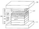
図1は、本発明の第1の実施の形態に係る磁気抵抗効果素子(CCP−CPP素子)を表す斜視図である。なお、図1および以降の図は全て模式図であり、図上での膜厚同士の比率と、実際の膜厚同士の比率は必ずしも一致しない。
図1に示すように本実施の形態に係る磁気抵抗効果素子は、磁気抵抗効果膜10、およびこれを上下から夾む下電極11および上電極20を有し、図示しない基板上に構成される。Hereinafter, embodiments of the present invention will be described with reference to the drawings. In the following embodiments, the composition of the alloy is expressed in atomic%.
(First embodiment)
FIG. 1 is a perspective view showing a magnetoresistive effect element (CCP-CPP element) according to a first embodiment of the present invention. Note that FIG. 1 and the subsequent drawings are all schematic views, and the ratio between the film thicknesses in the figure does not necessarily match the ratio between the actual film thicknesses.
As shown in FIG. 1, the magnetoresistive effect element according to the present embodiment has a
磁気抵抗効果膜10は、下地層12、ピニング層13、ピン層14、下部金属層15、スペーサ層(CCP−NOL)16、上部金属層17、フリー層18、キャップ層19が順に積層されて構成される。この内、ピン層14、スペーサ層16、およびフリー層18が、全体として、二つの強磁性層の間に非磁性のスペーサ層を挟んでなるスピンバルブ膜に対応する。なお、見やすさのために、スペーサ層16はその上下層(下部金属層15および上部金属層17)から切り離した状態で表している。
本実施形態では、ピン層14、およびフリー層18の少なくとも一方にダンピングファクタ(DF)調整層21を挿入することで、STIノイズの低減を図っている。The
In this embodiment, the STI noise is reduced by inserting a damping factor (DF)
なお、図1のCCP−CPP素子はピン層14を下部に配置したボトム型であるが、ピン層14を上部に配置したトップ型でも差し支えない。即ち、下電極11、下地層12〜キャップ層19、および上電極20の積層構造の上下を逆転することが可能である。 The CCP-CPP element in FIG. 1 is a bottom type in which the pinned layer 14 is disposed at the bottom, but may be a top type in which the pinned layer 14 is disposed at the top. That is, it is possible to reverse the top and bottom of the laminated structure of the
以下、磁気抵抗効果素子の構成要素を説明する。
下電極11は、スピンバルブ膜の垂直方向に通電するための電極である。下電極11と上電極20との間に電圧が印加されることで、スピンバルブ膜内部をその膜垂直方向に沿って電流が流れる。この電流によって、磁気抵抗効果に起因する抵抗の変化を検出することで、磁気の検知が可能となる。具体的な材料としては、下シールドと兼用したNiFeや、非磁性のCu,Ta,Ru、Crなどの金属層が用いられる。Hereinafter, components of the magnetoresistive element will be described.
The
下地層12は、例えば、バッファ層12a、シード層12bに区分することができる。バッファ層12aは下電極11表面の荒れを緩和したりするための層である。シード層12bは、その上に成膜されるスピンバルブ膜の結晶配向および結晶粒径を制御するための層である。 The
バッファ層12aとしては、Ta、Ti、W、Zr、Hf、Crまたはこれらの合金を用いることができる。バッファ層12aの膜厚は2〜10nm程度が好ましく、3〜5nm程度がより好ましい。バッファ層12aの厚さが薄すぎるとバッファ効果が失われる。一方、バッファ層12aの厚さが厚すぎるとMR変化率に寄与しない直列抵抗を増大させることになるので好ましくない。なお、バッファ層12a上に成膜されるシード層12bがバッファ効果も有する場合には、バッファ層12aを必ずしも設ける必要はない。 As the buffer layer 12a, Ta, Ti, W, Zr, Hf, Cr, or an alloy thereof can be used. The thickness of the buffer layer 12a is preferably about 2 to 10 nm, and more preferably about 3 to 5 nm. If the buffer layer 12a is too thin, the buffer effect is lost. On the other hand, if the buffer layer 12a is too thick, the series resistance that does not contribute to the MR ratio is increased, which is not preferable. In addition, when the seed layer 12b formed on the buffer layer 12a also has a buffer effect, the buffer layer 12a is not necessarily provided.
シード層12bは、その上に成膜される層の結晶配向を制御できる材料であればよいが、hcp構造(hexagonal close-packed structure:六方最密構造)またはfcc構造(face-centered cubic structure:面心立方構造)を有する金属層などが好ましい。シード層12bとして、Ruを用いることにより、その上のスピンバルブ膜の結晶配向をfcc(111)配向にすることができる。また、ピニング層13(例えば、PtMn)の結晶配向を規則化したfct構造(face-centered tetragonal structure:面心正方構造)、あるいはbcc(body-centered cubic structure:体心立方構造)(110)配向とすることができる。 The seed layer 12b may be any material that can control the crystal orientation of a layer formed thereon, but it may have an hcp structure (hexagonal close-packed structure) or an fcc structure (face-centered cubic structure: A metal layer having a face-centered cubic structure is preferred. By using Ru as the seed layer 12b, the crystal orientation of the spin valve film thereon can be changed to the fcc (111) orientation. Further, the fct structure (face-centered tetragonal structure) in which the crystal orientation of the pinning layer 13 (for example, PtMn) is regularized, or bcc (body-centered cubic structure) (110) orientation It can be.
スピンバルブ膜やピニング層13の結晶配向性は、X線回折により測定できる。スピンバルブ膜のfcc(111)ピーク、ピニング層13(PtMn)のfct(111)ピークまたはbcc(110)ピークでのロッキングカーブの半値幅を3.5〜6度として、良好な配向性を得ることができる。なお、この配向の分散角は断面TEMを用いた回折スポットからも判別することができる。 The crystal orientation of the spin valve film and the pinning
また、シード層12bを設けることにより、スピンバルブ膜の結晶粒径を10〜40nmに制御することができ、CCP−CPP素子のサイズが小さくなっても特性のばらつきを招くことなく高MR変化率を実現できる。 In addition, by providing the seed layer 12b, the crystal grain size of the spin valve film can be controlled to 10 to 40 nm, and even if the size of the CCP-CPP element is reduced, a high MR change rate without causing variation in characteristics. Can be realized.
シード層12bとして、Ruの代わりに、例えばNixFe100−x(x=90〜50%、好ましくは75〜85%)や、NiFeに第3元素Xを添加して非磁性にした(NixFe100−x)100−yXy(X=Cr、V、Nb、Hf、Zr、Mo)などのNiFeベースの合金を用いることもできる。Ruよりも、NiFeベースのほうが、シード層12bとして良好な結晶配向性を得るのがより容易であり、上記と同様に測定したロッキングカーブの半値幅を3〜5度とすることができる。As the seed layer 12b, instead of Ru, for example, Nix Fe100-x (x = 90 to 50%, preferably 75 to 85%) or the third element X is added to NiFe to make it nonmagnetic (Nix Fe 100-x) 100- y X y (X = Cr, V, Nb, Hf, Zr, Mo) can also be used NiFe-based alloy such as. It is easier for the NiFe base to obtain better crystal orientation as the seed layer 12b than Ru, and the half width of the rocking curve measured in the same manner as described above can be 3 to 5 degrees.
上述した10〜40nmという適正な結晶粒径を得るためには、第3元素Xの組成yを0〜30%程度とすることが好ましい(yが0%の場合も含む)。結晶粒径を40nmよりも粗大化させるためには、さらに多量の添加元素を用いることが好ましい。例えば、NiFeCrの場合にはCr量を35〜45%程度とし、fccとbccの境界相を示す組成を用いることが好ましい。 In order to obtain an appropriate crystal grain size of 10 to 40 nm as described above, the composition y of the third element X is preferably about 0 to 30% (including the case where y is 0%). In order to make the crystal grain size coarser than 40 nm, it is preferable to use a larger amount of additive element. For example, in the case of NiFeCr, it is preferable to use a composition having a Cr amount of about 35 to 45% and a boundary phase between fcc and bcc.
ただし、高密度記録に対応した再生ヘッドとして用いる場合には、素子サイズが100nm以下になるので、結晶粒径が大きすぎると特性のばらつきを招くことがあり、大きな結晶粒を用いることはあまり好ましくない。一方、例えばMRAMとして用いる場合には、素子サイズが100nm以上の場合があるので、結晶粒径を粗大化させるシード層12bを用いてもよい。 However, when used as a reproducing head compatible with high-density recording, the element size is 100 nm or less, and if the crystal grain size is too large, there may be variations in characteristics, and it is not preferable to use large crystal grains. Absent. On the other hand, when used as an MRAM, for example, the element size may be 100 nm or more, and therefore a seed layer 12b for increasing the crystal grain size may be used.
シード層12bの膜厚は1.5nm〜6nm程度が好ましく、2〜4nmがより好ましい。シード層12bの厚さが薄すぎると結晶配向制御などの効果が失われる。一方、シード層12bの厚さが厚すぎると直列抵抗の増大を招くうえに、スピンバルブ膜の界面凹凸の原因となることがある。 The thickness of the seed layer 12b is preferably about 1.5 nm to 6 nm, and more preferably 2 to 4 nm. If the thickness of the seed layer 12b is too thin, effects such as crystal orientation control are lost. On the other hand, if the seed layer 12b is too thick, the series resistance may be increased and the interface irregularity of the spin valve film may be caused.
ピニング層13は、その上に成膜されるピン層14となる強磁性層に一方向異方性を付与して磁化を固着する機能を有する。ピニング層13の材料としては、PtMn、PdPtMn、IrMn、RuRhMnなどの反強磁性材料を用いることができる。
十分な強さの一方向異方性を付与するために、ピニング層13の膜厚を適切に設定する。ピニング層13がPtMnやPdPtMnの場合には、膜厚は8〜20nm程度が好ましく、10〜15nmがより好ましい。ピニング層13がIrMnやRuRhMnの場合には、PtMnなどより薄い膜厚でも一方向異方性を付与することができるので、5〜18nmが好ましく、7〜15nmがより好ましい。The pinning
In order to impart sufficient strength of unidirectional anisotropy, the film thickness of the pinning
PtMn等の反強磁性層の比抵抗は概ね100μΩcm以上と大きいため、ピニング層13がMR変化率に直接寄与しない直列抵抗を増大させ、RAの値を大きくする要因になる可能性がある。直列抵抗の増加を防止するために、ピニング層13として、反強磁性層の代わりに、ハード磁性層を用いることができる。ハード磁性層としては、例えばCoPt(Co=50〜85%)、(CoxPt100−x)100−yCry(x=50〜85%、y=0〜40%)、FePt(Pt40〜60%)などを用いることができる。ハード磁性層(特にCoPt)は比抵抗が比較的小さいため、直列抵抗およびRAの増大を抑制できる。Since the specific resistance of the antiferromagnetic layer such as PtMn is as large as about 100 μΩcm or more, there is a possibility that the pinning
ピン層14は、下部ピン層141(例えば、Co90Fe10)、磁気結合層142(例えば、Ru)、および上部ピン層143(例えば、Co90Fe10[4nm])からなる3層構造のシンセティックピン層とすることができる。ピニング層13(例えば、PtMn)とその直上の下部ピン層141は一方向異方性をもつように交換磁気結合している。磁気結合層142の上下の下部ピン層141および上部ピン層143は、磁化の向きが互いに反平行になるように強く磁気結合している。The pinned layer 14 has a three-layer structure including a lower pinned layer 141 (for example, Co90 Fe10 ), a magnetic coupling layer 142 (for example, Ru), and an upper pinned layer 143 (for example, Co90 Fe10 [4 nm]). It can be a synthetic pinned layer. The pinning layer 13 (for example, PtMn) and the lower pinned
下部ピン層141には、例えばCoxFe100−x合金(x=0〜100%)、NixFe100−x合金(x=0〜100%)、またはこれらに非磁性元素を添加したものを用いることができる。The lower pinned
下部ピン層141は、磁気膜厚すなわち飽和磁化Bs×膜厚t(Bs・t積)が、上部ピン層143とほぼ等しくなるように設計することが好ましい。一例として、上部ピン層143が(Fe50Co50[1nm]/Cu[0.25nm])×2/Fe50Co50[1nm]の場合には、FeCoの飽和磁化が約2.2Tであるため、磁気膜厚は2.2T×3nm=6.6Tnmとなる。下部ピン層141についてはCo90Fe10の飽和磁化が約1.8Tなので、上記と等しい磁気膜厚を与える下部ピン層141の膜厚tは6.6Tnm/1.8T=3.66nmとなる。したがって、膜厚が約3.6nmのCo90Fe10を用いることが望ましい。The lower pinned
下部ピン層141に用いられる磁性層の膜厚は2〜5nm程度が好ましい。ピニング層13(例えば、PtMn)による一方向異方性磁界強度およびRuを介した下部ピン層141と上部ピン層143との反強磁性結合磁界強度という観点に基づく。下部ピン層141が薄すぎるとMR変化率が小さくなる。一方、下部ピン層141が厚すぎるとデバイス動作に必要な十分な一方向性異方性磁界を得ることが困難になる。 The thickness of the magnetic layer used for the lower pinned
磁気結合層142(例えば、Ru)は上下の磁性層に反強磁性結合を生じさせてシンセティックピン構造を形成する機能を有する。磁気結合層142としてのRu層の膜厚は0.8〜1nmであることが好ましい。なお、上下の磁性層(下部ピン層141および上部ピン層143)に十分な反強磁性結合を生じさせる材料であれば、Ru以外の材料を用いてもよい。 The magnetic coupling layer 142 (for example, Ru) has a function of forming an antiferromagnetic coupling in the upper and lower magnetic layers to form a synthetic pin structure. The film thickness of the Ru layer as the magnetic coupling layer 142 is preferably 0.8 to 1 nm. A material other than Ru may be used as long as it is a material that causes sufficient antiferromagnetic coupling in the upper and lower magnetic layers (lower pinned
上部ピン層143(Co90Fe10[4nm])は、スピン依存散乱ユニットの一部をなす。上部ピン層143として、fcc構造をもつCo90Fe10の換わりに、bcc構造をもつFeCoなどを用いた場合、スピン依存界面散乱効果が大きいため、大きなMR変化率を実現することができる。bcc構造をもつFeCo系合金としては、FexCo100−x(x=30〜100%)や、FexCo100−xに添加元素を加えたものが挙げられる。スピンバルブ膜に用いられる金属材料は、fcc構造またはfct構造であることが多いため、上部ピン層143のみがbcc構造を有することがあり得る。The upper pinned layer 143 (Co90 Fe10 [4 nm]) forms part of the spin-dependent scattering unit. When FeCo having a bcc structure or the like is used as the upper pinned
上部ピン層143の膜厚が薄すぎると、bcc構造を安定に保つことが困難になり、高いMR変化率が得られなくなるので、上部ピン層143の膜厚は2nm以上であることが好ましい。一方、大きなピン固着磁界を得るために、上部ピン層143の膜厚は5nm以下であることが好ましい。
上部ピン層143が高MR変化率を実現しやすいbcc構造をもつ磁性層から形成されている場合には、bcc構造をより安定に保つために、bcc構造をもつ層の膜厚は2nm以上であることが好ましい。If the film thickness of the upper pinned
When the upper pinned
大きなピン固着磁界とbcc構造の安定性とを両立させるには、bcc構造をもつ層の膜厚は2.5nm〜4nm程度が好ましい。FeCo系の磁性膜に関しては、相図上でより安定なbcc構造が得られる組成範囲として、Fe75Co25〜Fe85Co15が挙げられる。In order to achieve both a large pinned magnetic field and the stability of the bcc structure, the thickness of the layer having the bcc structure is preferably about 2.5 nm to 4 nm. Regarding FeCo-based magnetic films, Fe75 Co25 to Fe85 Co15 can be cited as a composition range in which a more stable bcc structure can be obtained on the phase diagram.
上部ピン層143には、bcc構造をもつ磁性材料の代わりに、fcc構造のCoFe合金や、hcp構造をもつコバルト合金も用いることができる。Co、Fe、Niなどの単体金属、またはこれらのいずれか一つの元素を含む合金材料はすべて用いることができる。上部ピン層143の磁性材料として、大きなMR変化率を得るのに有利なものから並べると、bcc構造をもつ合金材料、50%以上のコバルト組成をもつコバルト合金、50%以上のNi組成をもつニッケル合金の順になる。
上部ピン層143中にダンピングファクタ(DF)調整層21を挿入して、STIノイズの抑制を図ることができる。この詳細は後述する。For the upper pinned
A damping factor (DF)
下部金属層15は、電流パス162を形成するときに用いられ、いわば電流パス162の供給源である。ただし、電流パス162の形成後にも明確な金属層として残存している必要はない。 The
スペーサ層(CCP−NOL)16は、絶縁層161、電流パス162を有する。なお、スペーサ層16、下部金属層15、および上部金属層17を含めて、スペーサ層として取り扱うことも可能である。
絶縁層161は、酸化物、窒化物、酸窒化物等から構成され、アモルファスから形成されるAl2O3もあれば、MgOのような結晶構造を有する場合もある。The spacer layer (CCP-NOL) 16 includes an insulating
The insulating
絶縁層161に用いる典型的な絶縁材料として、Al2O3をベース材料としたものや、これに添加元素を加えたものがある。添加元素として、Ti、Hf、Mg、Zr,V,Mo、Si,Cr,Nb,Ta,W、B,Cなどがある。これらの添加元素の割合は0%〜50%程度の割合で適宜変えて用いることができる。As a typical insulating material used for the insulating
絶縁層161には、Al2O3のようなAl酸化物の換わりに、Ti酸化物、Hf酸化物、Mg酸化物、Zr酸化物、Cr酸化物、V酸化物、Ta酸化物、Nb酸化物、Mo酸化物、Si酸化物なども用いることができる。これらの酸化物の場合でも、添加元素として上述したような材料を用いることができる。また、添加元素の量としても0%〜50%程度の割合で適宜変えて用いることができる。
これら酸化物の換わりに、上述したようなAl,Si,Hf,Ti,Mg,Zr,V,Mo,Nb,Ta,W,B,Cをベースとした酸窒化物や、窒化物を用いても良い。For the insulating
Instead of these oxides, oxynitrides and nitrides based on Al, Si, Hf, Ti, Mg, Zr, V, Mo, Nb, Ta, W, B, and C as described above are used. Also good.
電流パス162は、電流を狭窄するためのものであり、絶縁層161の層方向に電流を通過させる導電体として機能し、例えば、Cu等の非磁性金属から構成できる。即ち、スペーサ層16は電流狭窄構造(CCP構造)を有する。電流狭窄効果により素子抵抗およびMR変化率を増大させることができる。
電流パス162は絶縁層161と比べて著しく酸素、窒素の含有量が少ない領域であり(少なくとも2倍以上の酸素や窒素の含有量の差がある)、一般的には結晶相である。結晶相は非結晶相よりも抵抗が小さいため、電流パス162として機能しやすい。The
The
上部金属層17は、その上に成膜されるフリー層18がスペーサ層16の酸化物に接して酸化されないように保護するバリア層としての機能を有する。
なお、フリー層18の酸化はアニール条件の最適化などによって回避可能なので、必ずしも上部金属層17を設けなくてもよい。しかし、製造上のマージンを考慮すると、スペーサ層16上に上部金属層17を形成することが好ましい。The upper metal layer 17 functions as a barrier layer that protects the
Since the oxidation of the
上部金属層17の構成材料として、Cu以外に、Au、Ag、Ruなどを用いることもできる。上部金属層17の材料は、スペーサ層16の電流パス162の材料と同一であることが好ましい。上部金属層17の材料が電流パス162の材料と異なる場合には界面抵抗の増大を招くが、両者が同一の材料であれば界面抵抗の増大は生じない。
上部金属層17の膜厚は、0〜1nmが好ましく、0.1〜0.5nmがより好ましい。上部金属層17が厚すぎると、スペーサ層16で狭窄された電流が上部金属層17で広がって電流狭窄効果が不十分になり、MR変化率の低下を招く。As a constituent material of the upper metal layer 17, Au, Ag, Ru, or the like can be used in addition to Cu. The material of the upper metal layer 17 is preferably the same as the material of the
The thickness of the upper metal layer 17 is preferably 0 to 1 nm, and more preferably 0.1 to 0.5 nm. If the upper metal layer 17 is too thick, the current confined by the spacer layer 16 spreads in the upper metal layer 17 and the current confinement effect becomes insufficient, leading to a reduction in MR ratio.
フリー層18は、磁化方向が外部磁界によって変化する強磁性体を有する層であり、例えば、界面にCoFeを挿入してNiFeを用いたCo90Fe10[1nm]/Ni83Fe17[3.5nm]という3層を用いてもよい。高いMR変化率を得るためには、スペとーサ層16の界面に位置するフリー層18の磁性材料の選択が重要である。この場合、スペーサ層16との界面には、NiFe合金よりもCoFe合金を設けることが好ましい。なお、NiFe層を用いない場合には、Co90Fe10[4nm]を用いることができる。
CoFe合金のなかでも、軟磁気特性が安定であることから、Co90Fe10が好ましい。Co90Fe10近傍のCoFe合金を用いる場合には、膜厚を0.5〜4nmとすることが好ましい。
また、フリー層18として、1〜2nmのCoFe層またはFe層と、0.1〜0.8nm程度の極薄Cu層とを、複数層交互に積層したものを用いてもよい。The
Among the CoFe alloys, Co90 Fe10 is preferable because the soft magnetic characteristics are stable. When a CoFe alloy near Co90 Fe10 is used, the film thickness is preferably 0.5 to 4 nm.
Further, as the
フリー層18の場合においても、ピン層14の場合と同様に、スペーサ層16がCu層から形成される場合には、bccのFeCo層をスペーサ層16との界面材料として用いるとMR変化率が大きくなるので、スペーサ層16との界面材料として、fccのCoFe合金の換わりにbccのFeCo合金を用いることもできる。この場合にはbcc層が形成されやすい、FexCo100−x(x=30〜100)や、これに添加元素を加えた材料も用いることができる。
ここで、これらのフリー層18中にダンピングファクタ(DF)調整層21を挿入して、STIノイズの抑制を図ることができる。この詳細は後述する。Also in the case of the
Here, a damping factor (DF)
キャップ層19は、スピンバルブ膜を保護する機能を有する。キャップ層19は、例えば、複数の金属層、例えば、Cu層とRu層の2層構造とすることができる。このときCu層の膜厚は0.5〜10nm程度が好ましい。また、Ru層の膜厚を0.5〜10nm程度とすることができる。
キャップ層19として、Cu層を用いず、0.5〜10nm程度の厚さのRu層をフリー層18上に直接設けてもよい。また、Ru層の代わりに他の金属層を設けてもよい。キャップ層19の構成は特に限定されず、キャップとしてスピンバルブ膜を保護可能なものであれば、他の材料を用いてもよい。The
As the
上電極20は、スピンバルブ膜の垂直方向に通電するための電極である。下電極11と上電極20との間に電圧が印加されることで、スピンバルブ膜内部をその膜垂直方向に沿って電流が流れる。 The
(ダンピングファクタ(DF)調整層21の詳細)
ダンピングファクタ調整層21はSTIノイズを低減するための層である。前述したように、磁化方向を動かそうとするトルクによって、STIノイズが発生する。スピントルクを持った電子(簡易的な言い方をすると、磁性層の磁化情報をもった電子)がピン層14からフリー層18もしくはその逆向きに流れることで、磁化情報を互いに平行に揃える方向、もしくは反平行の向きに揃えるトルクが発生し、このトルクがノイズの原因となる。このような磁化方向を動かそうとするトルクを抑制すること(電流通電による磁化トルクを安定させること)がSTIノイズの低減に有効である。このトルクへのダンピングを表すパラメータがダンピングファクタである。(Details of damping factor (DF) adjustment layer 21)
The damping
本実施形態では、ダンピングファクタを増大させて、STIノイズを低減し、しかもMR変化率を高い値に維持することが可能である。具体的な手法として、CCP−CPPスピンバルブ膜の磁性層中に、ダンピングファクタ調整層21として、例えば、0.5nm程度の極薄のPt層を挿入する。これによりスピントランスファートルク現象、ひいてはSTIノイズが抑制される。 In this embodiment, it is possible to increase the damping factor to reduce STI noise and to maintain the MR change rate at a high value. As a specific method, for example, an ultrathin Pt layer of about 0.5 nm is inserted as the damping
ここで、ダンピングファクタ調整層21として、原子番号が大きな材料、または非磁性3d遷移金属の極薄層を用いることが、ダンピングファクタを上昇させるために有効である。ダンピングファクタ調整層21は、ピン層14、またはフリー層18に挿入される。 Here, it is effective to use a material having a large atomic number or a non-magnetic 3d transition metal ultrathin layer as the damping
しかしながら、通常のメタルCPPスピンバルブ膜の磁性層に大きな原子番号の材料を混入させることは、弊害をもたらす危険性がある。具体的には、大きな原子番号を有する材料を磁性層に混入させると、スピン軌道相互作用によってGMR効果が減少する。特に、メタルCPPスピンバルブ膜においては、GMR効果への影響が顕著である。これは、CPP−GMRでは、スピン依存界面散乱効果とスピン依存バルク散乱効果の二つがあるが、通常のメタルCPPスピンバルブ膜ではスピン依存バルク散乱効果の方が顕著であることに起因する。 However, mixing a material having a large atomic number into the magnetic layer of a normal metal CPP spin valve film has a risk of causing adverse effects. Specifically, when a material having a large atomic number is mixed in the magnetic layer, the GMR effect is reduced by the spin orbit interaction. In particular, in the metal CPP spin valve film, the influence on the GMR effect is significant. This is because the CPP-GMR has a spin-dependent interface scattering effect and a spin-dependent bulk scattering effect, but the spin-dependent bulk scattering effect is more prominent in a normal metal CPP spin valve film.
スピン依存界面散乱効果は、スペーサ層16と、ピン層14、もしくはフリー層18の界面におけるGMR効果であり、界面近傍のみで生じる現象である。それに対し、スピン依存バルク散乱効果は、ピン層14、もしくはフリー層18の磁性層内部で生じるGMR効果である。スピン依存バルク散乱効果は磁性層内での現象であるため、磁性層の膜厚が厚いほうが、スピン依存バルク散乱効果が大きくなり、MR変化率が大きくなる。 The spin-dependent interface scattering effect is a GMR effect at the interface between the spacer layer 16 and the pinned layer 14 or the
通常のメタルCPPスピンバルブ膜においては、スピン依存界面散乱効果によるGMR現象は小さく、GMR現象のほとんどがスピン依存バルク散乱効果に起因する(非特許文献3:H. Yuasa et al., J. Appl. Phys. 92 (5), 2646 (2002))。この非特許文献3のFig5で、磁性層膜厚がゼロの極限でのAdR(面積抵抗変化量)に比べて(この値がスピン依存界面散乱効果に相当)、磁性層膜厚が厚いところでのAdRのほうがはるかに大きいこと(磁性層膜厚が厚いところではスピン依存界面散乱効果とスピン依存バルク散乱効果の和をみていることになる)から、この事実を理解することができる。 In a normal metal CPP spin valve film, the GMR phenomenon due to the spin-dependent interface scattering effect is small, and most of the GMR phenomenon is caused by the spin-dependent bulk scattering effect (Non-Patent Document 3: H. Yuasa et al., J. Appl. Phys. 92 (5), 2646 (2002)). In FIG. 5 of Non-Patent Document 3, compared to AdR (area resistance change amount) in the limit where the magnetic layer thickness is zero (this value corresponds to the spin-dependent interface scattering effect), the magnetic layer thickness is larger. This fact can be understood from the fact that AdR is much larger (the sum of the spin-dependent interface scattering effect and the spin-dependent bulk scattering effect is seen where the magnetic layer is thick).
つまり、通常のメタルCPPスピンバルブ膜においては、スピンバルク散乱効果の寄与が非常に大きい。このため、スピン依存バルク散乱効果を低下させる大きな原子番号の材料を磁性層に挿入することは、MR変化率の低下、ひいてはヘッド出力の低下、という観点において好ましくない。即ち、低STIノイズと高出力の両立が困難である。このように、通常のメタルスペーサ層16を有するメタルCPPスピンバルブ膜において、大きな原子番号の元素をピン層14もしくはフリー層18の磁性層に挿入するのは好ましい手法とは言いにくい。 That is, in the normal metal CPP spin valve film, the contribution of the spin bulk scattering effect is very large. For this reason, it is not preferable to insert a material having a large atomic number that reduces the spin-dependent bulk scattering effect into the magnetic layer from the viewpoint of a decrease in MR ratio and a decrease in head output. That is, it is difficult to achieve both low STI noise and high output. Thus, in a metal CPP spin valve film having a normal metal spacer layer 16, it is difficult to say that inserting an element having a large atomic number into the magnetic layer of the pinned layer 14 or the
一方、CCP−CPPスピンバルブ膜においては、スピン依存バルク散乱効果よりも、スピン依存界面散乱効果の影響のほうがはるかに大きい(非特許文献4:H. Fukuzawa et al., Appl. Phys. Lett. 87, 082507 (2005))。これは、スピンバルブ膜のトータル抵抗に占める、CCP部分の寄与が非常に大きいため、CCP近傍での界面効果の影響が大きいことに起因する。つまり、CCP−CPPスピンバルブ膜においては、多少のスピン依存バルク散乱効果の低下があったとしても、スピン依存界面散乱効果の低下が起こらなければ、MR変化率およびヘッド出力の低下は生じにくい。このため、低STIノイズと高いMR変化率の両立を図ることが容易となる。
上記の理由によって、CCP−CPP素子において、ダンピングファクタ調整層21によって、MRを事実上低下させることなく、STIノイズを抑制することが可能となる。On the other hand, in the CCP-CPP spin valve film, the influence of the spin-dependent interface scattering effect is much greater than the spin-dependent bulk scattering effect (Non-patent Document 4: H. Fukuzawa et al., Appl. Phys. Lett. 87, 082507 (2005)). This is because the influence of the interface effect in the vicinity of the CCP is large because the contribution of the CCP portion to the total resistance of the spin valve film is very large. That is, in the CCP-CPP spin valve film, even if there is a slight decrease in the spin-dependent bulk scattering effect, the MR ratio and the head output are unlikely to decrease unless the spin-dependent interface scattering effect decreases. For this reason, it is easy to achieve both low STI noise and a high MR ratio.
For the above reason, in the CCP-CPP element, the damping
ダンピングファクタ調整層21としては、Pt以外にもZr,Nb,Mo,Ru,Rh,Pd,Ag,La,Hf,Ta,W,Re,Os,Ir,Pt,Auなどの原子番号が比較的大きな材料や、非磁性のTi、V、Cr、Mnなどの3d遷移金属も用いることができる。 As the damping
非磁性材料を挿入することで、ピン層14、またはフリー層18内(即ち、ダンピングファクタ調整層21を介した上下磁性層間)での磁気結合が分断される可能性がある。ダンピングファクタ調整層21を介した磁気結合を十分大きな値として保つためには、ダンピングファクタ調整層21の膜厚として、0.1〜1nm、さらに好ましくは0.1nm〜0.7nmが好ましい。 By inserting a nonmagnetic material, there is a possibility that the magnetic coupling in the pinned layer 14 or the free layer 18 (that is, the upper and lower magnetic layers via the damping factor adjusting layer 21) may be broken. In order to keep the magnetic coupling through the damping
ダンピングファクタ調整層21はピン層14、フリー層18のいずれか一方のみに挿入されていても差し支えない。
スペーサ層16の近傍にダンピングファクタ調整層21を挿入すると、MR変化率の減少を招き好ましくない。スペーサ層16から少なくとも1nm以上離れた位置に、ダンピングファクタ調整層21を挿入することが好ましい。即ち、MR変化率への影響を考慮し、スペーサ層16からある程度離れた位置にダンピングファクタ調整層21を配置する。The damping
If the damping
このように、スペーサ層16との界面近傍から1nm程度離れた位置にダンピングファクタ調整層21が配置されることによって、スピン依存界面散乱効果には悪影響を与えることなく、ダンピングファクタを抑制することができる。つまり、CCP−CPPの場合にはMR変化率を犠牲にすることなく、効率的にSTIノイズを抑制することが可能となる。 As described above, the damping
材料によっては、スペーサ層16との界面近傍から1nm以下の領域にダンピングファクタ調整層21を挿入することも可能である。具体的には、Ti、Zr、PdやNbなどをダンピングファクタ調整層21として用いたときには、比較的スピン依存界面散乱効果の影響を乱すことがないので、スペーサ層16との界面から1nm以下の領域にダンピングファクタ調整層21を挿入しても構わない。より具体的には、スペーサ層16との界面(つまり界面から0nmの距離)から1nmまでの距離における挿入位置でも用いることができる。当然のことながら、これらの材料は、それよりも離れた距離など、任意の位置に挿入することが可能ある。
MR変化率への影響が少ない、という観点において、これらTi、Zr、Pd、Nbなどの材料はダンピングファクタ調整層21として用いやすい材料である。Depending on the material, it is also possible to insert the damping
These materials such as Ti, Zr, Pd, and Nb are materials that can be easily used as the damping
ダンピングファクタ調整層21はピン層14、もしくはフリー層18といった磁性層に複数層挿入しても構わない。この場合には、上記Ti、Zr、Nbなどの材料を用いるときはスペーサ層16からの距離が1nm以下のところに第一層を挿入し、Pt等他の元素のときにはスペーサ層16からの距離が1nmよりも離れたところに第一層を挿入する。そして、第2層、第3層といった積層膜を前記第1層よりもスペーサ層16から離れた位置に挿入することになる。これら第1層と第2層、もしくは第2層と第3層との間の距離は、1nmから2nm程度が好ましい範囲である。しかし、厚い磁性層を用いる場合にはこの範囲よりも厚い間隔で用いることも可能である。 A plurality of damping factor adjustment layers 21 may be inserted in a magnetic layer such as the pinned layer 14 or the
フリー層18、もしくはピン層14内でダンピングファクタ調整層21を複数層用いることのメリットとして、ダンピングファクタ調整の効果、ひいてはノイズ低減の効果がより増大する点がある。ダンピングファクタ調整層21を複数層挿入するのは、フリー層18だけの場合でもよいし、ピン層14だけの場合でもよく、またピン層14、フリー層18両方を積層構成にしても構わない。 As an advantage of using a plurality of damping factor adjusting layers 21 in the
複数層のダンピングファクタ調整層21を用いるデメリットとして、MR変化率が低減したり、ダンピングファクタ調整層21を介した磁性層間の磁気結合が弱まったりすることで、磁気特性が悪くなる可能性がある。磁気特性を防止するため、フリー層18、もしくはピン層14内でのダンピングファクタ調整層21の膜厚の総量が、一層の場合と同様の膜厚範囲であることが好ましい。また、一つの磁性層内での複数のダンピングファクタ調整層21間の距離としては、上述したように、1〜2nmが好ましい範囲となる。 Disadvantages of using a plurality of damping factor adjustment layers 21 may be that the MR ratio is reduced or the magnetic coupling between the magnetic layers via the damping
ここで、本実施形態のような、ダンピングファクタ調整層21を用いる代わりに、磁性層(ピン層14、フリー層18)の構成材料自体に、ST効果が抑制されるような材料(例えば、合金材料)を選択することが考えられる。
しかし、この場合にはMR変化率が低下してしまう。CCP構造をもつCPPスピンバルブ膜ではスペーサ層16の界面近傍でのMR効果が大きく、この界面近傍にMR変化率を低下させるような添加元素が存在することは好ましくない。
スペーサ層16との界面近傍では高MR化を損なわない磁性材料を用い、磁性層(ピン層14、フリー層18)の内部に極薄の層(ダンピングファクタ調整層21)を挿入することでST効果を抑制できる。このようにすることで、ST効果の抑制と、MR変化率の維持とを両立することが容易となる。Here, instead of using the damping
However, in this case, the MR change rate decreases. In a CPP spin valve film having a CCP structure, the MR effect near the interface of the spacer layer 16 is large, and it is not preferable that an additive element that lowers the MR ratio be present near this interface.
In the vicinity of the interface with the spacer layer 16, a magnetic material that does not impair high MR is used, and an extremely thin layer (damping factor adjustment layer 21) is inserted inside the magnetic layer (pinned layer 14, free layer 18). The effect can be suppressed. By doing so, it becomes easy to achieve both suppression of the ST effect and maintenance of the MR ratio.
以下、本実施形態を比較例と対比して説明する。
A.Ptを磁性層全体に添加する場合との比較
比較例として、Ptを磁性層全体に添加元素として用いた場合を考える。フリー層18として用いる、CoFe/NiFeのような積層磁性層に、Ptを全体的に添加すると、CoFePt/NiFePtのフリー層18となる。この場合、ダンピングファクタが上昇し、STIノイズを抑制することができる。しかし、その一方では、MR変化率が低下するため、ヘッド出力の低下を招くことになる。具体的には、Pt添加しないフリー層においては、9%であったMR変化率が、Ptを添加したフリー層においては、4%となり、MR変化率が大幅に低下してしまう。Hereinafter, this embodiment will be described in comparison with a comparative example.
A. Comparison with the case where Pt is added to the entire magnetic layer As a comparative example, a case where Pt is used as an additive element to the entire magnetic layer is considered. When Pt is added as a whole to a laminated magnetic layer such as CoFe / NiFe used as the
一方、本実施形態では、Ptの極薄層をCCPの界面から少し遠ざかったところに挿入することで、大きなスピン依存界面散乱効果を維持したままで、ダンピングファクタ調整する効果が発揮される。具体的には、0.5nmの極薄Pt層をNiFe層中に挿入することで、MR変化率は8.5%と若干低下するが、さほど大きな低下ではなく、かつSTIノイズを大幅に抑制することが可能となる。即ち、本実施形態では、MR変化率が微減して信号出力が微減する影響よりも、ノイズが低減することでS/N比が向上するメリットの方が大きく、結果的にBER(Bit Error Rate)が低下し、良好な特性を得ることが可能となる。 On the other hand, in this embodiment, the effect of adjusting the damping factor is exhibited while maintaining a large spin-dependent interface scattering effect by inserting the Pt ultrathin layer at a distance from the CCP interface. Specifically, by inserting a 0.5 nm ultra-thin Pt layer into the NiFe layer, the MR change rate is slightly reduced to 8.5%, but this is not a significant decrease, and STI noise is greatly suppressed. It becomes possible to do. That is, in this embodiment, the advantage of improving the S / N ratio by reducing noise is greater than the effect of slightly reducing the MR change rate and the signal output, resulting in a BER (Bit Error Rate). ) Is reduced, and good characteristics can be obtained.
B.メタルCPPスピンバルブ膜の場合との比較
CCP構造を有しないメタルCPPスピンバルブ膜の場合には、スピン依存界面散乱効果が主ではなく、スピン依存バルク散乱効果が非常に大きな寄与となっている。このため、スペーサ層16の界面から遠ざかったところに極薄のPt層を挿入したとしても、MR変化率は低下してしまい、ダンピングファクタ調整層21としての機能を発揮することができない。B. Comparison with Metal CPP Spin Valve Film In the case of a metal CPP spin valve film having no CCP structure, the spin-dependent interface scattering effect is not the main effect, and the spin-dependent bulk scattering effect contributes very much. For this reason, even if an ultrathin Pt layer is inserted at a position away from the interface of the spacer layer 16, the MR change rate decreases, and the function as the damping
具体的な例を挙げると、CCPスペーサ層を有しない、5nmのCuスペーサ層を有する通常のメタルCPPスピンバルブ膜で、標準的なCoFe/NiFeフリー層の場合には、MR変化率は2%である。このとき、NiFe層中に0.5nmの極薄Pt層等を挿入すると、MR変化率は1%になってしまう。単純なメタルCPPスピンバルブ膜の場合には、もともとのMR変化率が1〜3%とただでさえ小さい値で、磁気ヘッドとして十分な出力を取りにくい。そして、このメタルCPPスピンバルブ膜にダンピングファクタ調整層21を挿入することによるMR変化率の劣化量は、CCP−CPPの場合よりも大きい。このため、トータルパフォーマンスとしては、メタルCPPスピンバルブ膜のダンピングファクタ調整層21として、極薄Pt層を用いることは困難である。
このように、CCPスピンバルブ膜とダンピングファクタ調整層21とを組み合わせることで、大きな効果が発揮される。As a specific example, in the case of a normal metal CPP spin valve film having a 5 nm Cu spacer layer without a CCP spacer layer and a standard CoFe / NiFe free layer, the MR ratio is 2%. It is. At this time, if a 0.5 nm ultrathin Pt layer or the like is inserted in the NiFe layer, the MR ratio will be 1%. In the case of a simple metal CPP spin-valve film, it is difficult to obtain a sufficient output as a magnetic head with an original MR change rate as small as 1 to 3%. The amount of MR change rate deterioration caused by inserting the damping
Thus, a great effect is exhibited by combining the CCP spin valve film and the damping
C.ダンピングファクタ調整層21を変更することによる影響
基本となるCCP−CPPスピンバルブ膜を固定し、ダンピングファクタ調整層21を変えたときのMR変化率への影響を検討する。
MR変化率に大きな影響を与えるピン層14、スペーサ層16、フリー層18の構成としては以下のような構成を用いて検討した。まず、ピン層143として、2〜3nmのFe50Co50に、0.2nmの極薄Cuを1nmのFeCoごとに積層したものを用いた。スペーサ層16は、CCP構造を有するAl2O3を絶縁層として用い、Cuをメタルパスとして用いた1.5〜2nmのスペーサ層16とした。フリー層18としては、CoFe 1nm/NiFe 3.5nmを基本膜構成とした。
このようなCCP−CPPスピンバルブ膜において、ダンピングファクタ調整層21を用いたときの、ダンピングファクタ調整層21の材料、および挿入位置依存性を示したものを以下の表1に示す。C. Effect of changing the damping
As the configurations of the pinned layer 14, the spacer layer 16, and the
In such a CCP-CPP spin valve film, Table 1 below shows the material and insertion position dependency of the damping

この表1は、ダンピングファクタ調整層21をフリー層18のみに挿入した場合の、材料、および挿入位置(距離:CCP界面からの距離)へのMR変化率の依存性を表す。なお、比較例0は、ダンピングファクタ調整層21を有しない場合である。
表1から判るように、Ptのような標準的なダンピングファクタ調整層21をスペーサ層16の界面に挿入した場合には、MR変化率は大きく減少し、有効とはいえない。通常は、スペーサ層16の界面から1nm以上離れた位置にダンピングファクタ調整層21を挿入することが望ましい。Table 1 shows the dependency of the MR ratio on the material and the insertion position (distance: distance from the CCP interface) when the damping
As can be seen from Table 1, when a standard damping
一方、ダンピングファクタ調整層21がTi,Zr,PdやHfの場合には、これをスペーサ層16の界面近傍に挿入してもMR変化率の減少の程度は比較的小さく、界面近傍においても用いることができる。しかしながら、界面よりも磁性層内部に挿入した場合のほうが、MR変化率減少への影響が少なくなるので、MR変化率の観点からは望ましい。 On the other hand, when the damping
具体的なSTIノイズの状況に応じて、界面近傍に設けるか、それとも磁性層内部に設けるかが最適化される。媒体の磁界に対する磁化応答はフリー層18が担い、ピン層14は媒体磁界の向きによらず磁化固着されているため、フリー層18にダンピングファクタ調整層21を挿入することがSTIノイズ低減に有効である。よって、実施例1〜11のようにフリー層18に挿入することが、MR変化率と、STIノイズ低減とが両立する構成として好ましい。 Depending on the specific STI noise situation, it is optimized whether it is provided near the interface or inside the magnetic layer. Since the
ピン層14のみにダンピングファクタ調整層21を挿入した場合の実施例21〜31を表2に示す。この場合も材料への依存性は定性的には実施例1〜11と同様である。しかしながら、ピン層14の場合にはスピン依存界面散乱効果が大きなbcc−FeCoを用いていることで、スピン依存界面散乱効果の上昇程度が大きい。このため、ダンピングファクタ調整層21を挿入することによるMR変化率の減少へのダメージはフリー層18の場合よりも大きくなる。 Examples 21 to 31 in the case where the damping
ピン層14、フリー層18ともに挿入した場合の実施例41〜51を表3に示す。傾向はこれまでと同様であり、ピン層14のみ、フリー層18のみに挿入した場合と比較すると、MR変化率の減少度合いは大きくなるが、STIノイズ抑制効果は大きくなる。 Tables 3 to 51 show Examples 41 to 51 when both the pinned layer 14 and the
(磁気抵抗効果素子の製造方法)
以下、本実施の形態における磁気抵抗効果素子の製造方法についてより詳細に説明する。
図2は、本発明の第1の実施形態に係る磁気抵抗効果素子の製造工程を表すフロー図である。
図3は、磁気抵抗効果素子の製造に用いられる成膜装置の概略を示す模式図である。また、図4は、この成膜装置中の酸化チャンバー60を表す模式図である。(Method for manufacturing magnetoresistive element)
Hereinafter, the manufacturing method of the magnetoresistive effect element in this Embodiment is demonstrated in detail.
FIG. 2 is a flowchart showing manufacturing steps of the magnetoresistive effect element according to the first embodiment of the present invention.
FIG. 3 is a schematic diagram showing an outline of a film forming apparatus used for manufacturing a magnetoresistive effect element. FIG. 4 is a schematic view showing an
図3に示すように、搬送チャンバー(TC)50を中心として、ロードロックチャンバー51、プレクリーニングチャンバー52、第1の金属成膜チャンバー(MC1)53、第2の金属成膜チャンバー(MC2)54、酸化チャンバー(OC)60がそれぞれゲートバルブを介して設けられている。この成膜装置では、ゲートバルブを介して接続された各チャンバーの間で、真空中において基板を搬送することができるので、基板の表面は清浄に保たれる。 As shown in FIG. 3, a
金属成膜チャンバー53,54は多元(5〜10元)のターゲットを有する。成膜方式は、DCマグネトロンスパッタ、RFマグネトロンスパッタ等のスパッタ法や、イオンビームスパッタ法、蒸着法などが挙げられる。 The metal
図4に示すように、酸化チャンバー60は真空ポンプ61によって真空引きされ、酸化チャンバー60にはマスフローコントローラー(MFC)63により流量制御された酸素ガスが酸素供給管62から導入される。
酸化チャンバー60内にはイオンソース70が設けられている。イオンソースの形式は、ICP(Inductive coupled plasma)型、Capacitive coupled plasma型、ECR(Electron-cyclotron resonance)型、カウフマン型などが挙げられる。As shown in FIG. 4, the
An
イオンソース70に対向するように基板ホルダー80および基板1が配置される。イオンソース70からのイオン放出口には、イオン加速度を調整する3枚のグリッド71、72、73が設けられている。イオンソース70の外側にはイオンを中和するニュートラライザ74が設けられている。基板ホルダー80は傾斜可能に支持されている。基板1へのイオンの入射角度は広い範囲で変えることができるが、典型的な入射角度の値は15°〜60°である。 The
以下、磁気抵抗効果素子の製造工程を説明する。
基板(図示せず)上に、下電極11、下地層12、ピニング層13、ピン層14、下部金属層15、スペーサ層16、上部金属層17、フリー層18、キャップ層19、上電極20を順に形成する。なお、形成の順序をこの逆とすることも可能である。Hereinafter, the manufacturing process of the magnetoresistive effect element will be described.
On a substrate (not shown), the
基板をロードロックチャンバー51にセットし、金属の成膜を金属成膜チャンバー53、54で、酸化を酸化チャンバー60でそれぞれ行う。金属成膜チャンバーの到達真空度は1×10⁻⁸Torr以下とすることが好ましく、5×10⁻¹⁰Torr〜5×10⁻⁹Torr程度が一般的である。搬送チャンバー50の到達真空度は10−9Torrオーダーである。酸化チャンバー60の到達真空度は8×10⁻⁸Torr以下である。The substrate is set in the
(1)下電極11、下地層12、ピニング層13の形成(ステップS11)
基板(図示せず)上に、下電極11を形成する。
下電極11上に、下地層12として、例えば、Ta[5nm]/Ru[2nm]を成膜する。既述のように、Taは下電極の荒れを緩和したりするためのバッファ層12aである。Ruはその上に成膜されるスピンバルブ膜の結晶配向および結晶粒径を制御するシード層12bである。(1) Formation of
A
On the
下地層12上にピニング層13を成膜する。ピニング層13の材料としては、PtMn、PdPtMn、IrMn、RuRhMnなどの反強磁性材料を用いることができる。 A pinning
(2)ピン層14(およびダンピングファクタ調整層21)の形成(ステップS12)
ピニング層13上にピン層14を形成する。ピン層14は、例えば、下部ピン層141(Co90Fe10)、磁気結合層142(Ru)、および上部ピン層143(Co90Fe10[4nm])からなるシンセティックピン層とすることができる。(2) Formation of pinned layer 14 (and damping factor adjusting layer 21) (step S12)
A pinned layer 14 is formed on the pinning
上部ピン層143の成膜の途中で、成膜する材料を切り換えることでダンピングファクタ調整層21を挿入することができる。具体的には、成膜材料をCo90Fe10からPtに切り換えて、またCo90Fe10に戻すことで、上部ピン層143中にPtからなるダンピングファクタ調整層21が挿入される。The damping
(3)スペーサ層16の形成(ステップS13)
次に、電流狭窄構造(CCP構造)を有するスペーサ層16を形成する。スペーサ層16を形成するには、酸化チャンバー60を用いる。
スペーサ層16を形成するには、以下のような方法を用いる。ここでは、アモルファス構造を有するAl2O3からなる絶縁層161中に金属結晶構造を有するCuからなる電流パス162を含むスペーサ層16を形成する場合を例に説明する。(3) Formation of spacer layer 16 (step S13)
Next, the spacer layer 16 having a current confinement structure (CCP structure) is formed. An
In order to form the spacer layer 16, the following method is used. Here, a case where the spacer layer 16 including the
1)上部ピン層143上に、電流パスの供給源となる下部金属層15(例えばCu)を成膜した後、下部金属層15上に絶縁層に変換される被酸化金属層(例えばAlCuやAl)を成膜する。 1) After forming a lower metal layer 15 (for example, Cu) serving as a current path supply source on the upper pinned
被酸化金属層に希ガス(例えばAr)のイオンビームを照射して前処理を行う。この前処理をPIT(Pre-ion treatmentという)。このPITの結果、被酸化金属層中に下部金属層の一部が吸い上げられて侵入した状態になる。 Pretreatment is performed by irradiating the metal layer to be oxidized with an ion beam of a rare gas (eg, Ar). This pretreatment is called PIT (Pre-ion treatment). As a result of this PIT, a part of the lower metal layer is sucked and invaded into the metal layer to be oxidized.
2)酸化ガス(例えば酸素)を供給して被酸化金属層を酸化する。この酸化により、被酸化金属層をAl2O3からなる絶縁層161に変換するとともに、絶縁層161を貫通する電流パス162を形成して、スペーサ層16を形成する。
例えば、希ガス(Ar、Xe、Kr、Heなど)のイオンビームを照射しながら酸化ガス(例えば酸素)を供給して被酸化金属層を酸化する(イオンビームアシスト酸化(IAO:Ion beam-assisted Oxidation))。この酸化処理により、絶縁層161であるAl2O3と電流パス162であるCuとが分離した形態のスペーサ層16が形成される。Alが酸化されやすく、Cuが酸化されにくいという、酸化エネルギーの差を利用した処理である。2) An oxidizing gas (for example, oxygen) is supplied to oxidize the metal layer to be oxidized. By this oxidation, the metal layer to be oxidized is converted into an insulating
For example, an oxidizing gas (for example, oxygen) is supplied while irradiating an ion beam of a rare gas (Ar, Xe, Kr, He, etc.) to oxidize a metal layer to be oxidized (ion beam assisted oxidation (IAO)). Oxidation)). By this oxidation treatment, the spacer layer 16 in a form in which the Al2 O3 as the insulating
(4)上部金属層17、フリー層18(およびダンピングファクタ調整層21)の形成(ステップS14)
スペーサ層16の上に、上部金属層17として、例えば、Cu[0.25nm]を成膜する。(4) Formation of upper metal layer 17 and free layer 18 (and damping factor adjusting layer 21) (step S14)
On the spacer layer 16, for example, Cu [0.25 nm] is formed as the upper metal layer 17.
上部金属層17の上に、フリー層18、例えば、Co90Fe10[1nm]/Ni83Fe17[3.5nm]を形成する。
フリー層18の成膜の途中で、成膜する材料を切り換えることでダンピングファクタ調整層21を挿入することができる。具体的には、成膜材料をNi83Fe17からPtに切り換えて、またNi83Fe17に戻すことで、フリー層18のNi83Fe17中にPtからなるダンピングファクタ調整層21が挿入される。A
The damping
(5)キャップ層19、および上電極20の形成(ステップS15)
フリー層18の上に、キャップ層19として例えば、Cu[1nm]/Ru[10nm]を積層する。キャップ層19の上にスピンバルブ膜へ垂直通電するための上電極20を形成する。(5) Formation of
On the
(実施例)
本発明の実施例の一例として、以下のような構成を挙げることができる。この実施例では、上部ピン層143中、およびフリー層18のFe50Co50層中に、ダンピングファクタ調整層21として、0.5nmのPt層を配置している。ダンピングファクタ調整層21を用いることで、RAが300〜1000mm2で、MR変化率が8〜15%という高い値を保持しつつ、STIノイズを抑制することが可能となる。
・下電極11
・下地層12:Ta[5nm]/Ru[2nm]
・ピニング層13:Pt50Mn50[15nm]
・ピン層14:Co90Fe10[4nm]/Ru[0.9nm]/Fe50Co50[2nm]/Pt0.5nm/Fe50Co50[2nm]
・下部金属層15:Cu[0.5nm]
・スペーサ層(CCP−NOL)16:Al2O3からなる絶縁層161およびCuからなる電流パス162(Al90Cu10[0.9nm]を成膜した後、酸化処理)
・上部金属層17:Cu[0.25nm]
・フリー層18:Co90Fe10[1nm]/Ni83Fe17[1nm]/Pt[0.5nm]/Ni83Fe17[1nm]
・キャップ層19:Cu[1nm]/Ru[10nm]
・ 上電極20(Example)
As an example of an embodiment of the present invention, the following configuration can be exemplified. In this embodiment, a 0.5 nm Pt layer is disposed as the damping
・
・ Underlayer 12: Ta [5 nm] / Ru [2 nm]
Pinning layer 13: Pt50 Mn50 [15 nm]
Pins layer14: Co 90 Fe 10 [4nm ] / Ru [0.9nm] /
Lower metal layer 15: Cu [0.5 nm]
Spacer layer (CCP-NOL) 16: Insulating
Upper metal layer 17: Cu [0.25 nm]
Free layer 18: Co90 Fe10 [1 nm] / Ni83 Fe17 [1 nm] / Pt [0.5 nm] / Ni83 Fe17 [1 nm]
Cap layer 19: Cu [1 nm] / Ru [10 nm]
・
(第2の実施の形態)
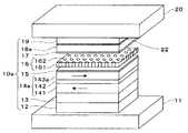
図5は、本発明の第2の実施の形態に係る磁気抵抗効果素子(CCP−CPP素子)を表す斜視図である。
図5に示すように本実施の形態に係る磁気抵抗効果素子は、磁気抵抗効果膜10a、およびこれを上下から夾む下電極11および上電極20を有し、図示しない基板上に構成される。
磁気抵抗効果膜10aは、下地層12、ピニング層13、ピン層14a、下部金属層15、スペーサ層(CCP−NOL)16、上部金属層17、フリー層18a、キャップ層19が順に積層されて構成される。磁気抵抗効果膜10aは、本質的に磁気抵抗効果膜10と異なる訳ではないので、これら下地層12〜キャップ層19の詳細な説明は省略する。(Second Embodiment)
FIG. 5 is a perspective view showing a magnetoresistive effect element (CCP-CPP element) according to the second embodiment of the present invention.
As shown in FIG. 5, the magnetoresistive effect element according to the present embodiment includes a magnetoresistive effect film 10a, and a
The magnetoresistive effect film 10a includes a
本実施形態では、フリー層18a上の界面(フリー層18aとキャップ層19の境界)に電子乱反射層(Diffusive Electron Scattering Layer: DESL)22を配置することで、STIノイズの低減を図っている。第1の実施形態と異なり、ピン層14aには電子乱反射層22は配置していない。
電子乱反射層22は、キャップ層19の下に配置され、電子を乱反射させる層である。電子乱反射層22で電子を乱反射させることで、強磁性層(フリー層18a)の外側界面(スペーサ層16とは反対側の界面)での電子反射を制限し、ST効果、ひいてはSTIノイズを抑制することができる。なお、電子乱反射層22をキャップ層19に含めて考えることも可能である。In this embodiment, an STI noise is reduced by disposing an electron diffuse reflection layer (Diffusive Electron Scattering Layer: DESL) 22 at an interface (a boundary between the free layer 18a and the cap layer 19) on the free layer 18a. Unlike the first embodiment, the electron
The electron
(1)非磁性アモルファス材料によって、電子乱反射層22を構成できる。非磁性アモルファス材料のアモルファス構造によって、電子を乱反射させ、STIノイズが抑制される。
非磁性アモルファス材料として、Ta、Ti、Zr、Hf、Nb、B、Si、Wなどの単体金属、またはこれらの元素を少なくとも50%以上含む合金材料を用いることができる。非磁性アモルファス材料として、AlBや、AlSiB、AlSiなどの合金組成によるアモルファス材料を用いても良い。(1) The electron
As the nonmagnetic amorphous material, a single metal such as Ta, Ti, Zr, Hf, Nb, B, Si, W, or an alloy material containing at least 50% of these elements can be used. As the nonmagnetic amorphous material, an amorphous material having an alloy composition such as AlB, AlSiB, or AlSi may be used.
非磁性アモルファス材料のアモルファス構造による電子の乱反射を利用してSTIノイズを抑制するため、電子乱反射層22が結晶構造を有することは好ましくない。電子乱反射層22内の結晶化を抑制するために、電子乱反射層22がある程度薄い方が好ましい。また、狭ギャップという観点からも、電子乱反射層22がある程度薄い方が好ましい。具体的には、電子乱反射層22の厚さとして0.5〜5nmが好ましく、1〜3nmがより好ましい。 Since the STI noise is suppressed by utilizing the irregular reflection of electrons due to the amorphous structure of the nonmagnetic amorphous material, it is not preferable that the electron
(2)また、ミキシング層によって、電子乱反射層22を構成できる。ミキシング層によって、電子の乱反射を発生させ、STIノイズを抑制できる。
2つの層を積層し、その界面にミキシング層を形成できる。即ち、相互に固溶な関係にある少なくとも二種以上の合金材料を2層にわけて積層し、その界面に固溶なミキシング層を形成できる。相互に固溶な材料の組み合わせとして、CuとAl(CuAl合金を形成)、CuとNi(CuNi合金を形成)などが挙げられる。(2) Moreover, the electron
Two layers can be laminated and a mixing layer can be formed at the interface. That is, at least two kinds of alloy materials having a solid solution relationship can be laminated in two layers, and a solid solution mixing layer can be formed at the interface. Examples of combinations of mutually solid materials include Cu and Al (form a CuAl alloy), Cu and Ni (form a CuNi alloy), and the like.
(磁気抵抗効果素子の製造方法)
図6は、本発明の第2の実施の形態に係る磁気抵抗効果素子の製造工程を表すフロー図である。
図6は、ダンピングファクタ調整層21に換えて電子乱反射層22を形成する点が図2と異なる。これ以外の点では、図6は図2と本質的に異なる訳ではないので、以下、電子乱反射層22の形成のみを説明する。(Method for manufacturing magnetoresistive element)
FIG. 6 is a flowchart showing the manufacturing process of the magnetoresistive effect element according to the second embodiment of the invention.
FIG. 6 differs from FIG. 2 in that an electron
図6のステップS25での電子乱反射層22の形成には次の手法(1)〜(3)のいずれかを適用できる。
(1)アモルファス層の形成
既述のTaなどの単体金属、これらの元素を少なくとも50%以上含む合金材料、AlBなどの合金材料を成膜することで、非磁性アモルファス材料の層が形成される。この成膜にDCマグネトロンスパッタ、RFマグネトロンスパッタ等のスパッタ法や、イオンビームスパッタ法、蒸着法を用いることができる。
なお、これらの材料はアモルファス化し易いことから、冷却等のアモルファス化を促進する手段を成膜時に適用しなくても差し支えない。Any of the following methods (1) to (3) can be applied to the formation of the electron
(1) Formation of amorphous layer A nonmagnetic amorphous material layer is formed by depositing the above-described simple metal such as Ta, an alloy material containing at least 50% of these elements, or an alloy material such as AlB. . For this film formation, sputtering methods such as DC magnetron sputtering and RF magnetron sputtering, ion beam sputtering, and vapor deposition can be used.
Since these materials are easily amorphized, means for promoting the amorphization such as cooling may not be applied at the time of film formation.
(2)ミキシング層の形成
1)既述のように、相互に固溶な関係にある少なくとも二種以上の合金材料を第1層、第2層にわけて積層することで、その界面に固溶なミキシング層を形成できる。この積層にDCマグネトロンスパッタ、RFマグネトロンスパッタ等のスパッタ法や、イオンビームスパッタ法、蒸着法を用いることができる。
例えば、フリー層18a上に、第1層としてAlを0.5nm、第2層としてCuを0.5nm、順に積層する。AlとCuは互いに固溶な関係にあるため、その界面においてミキシング層が形成され、このミキシング層で電子が乱反射される。
なお、Al[0.5nm]/Cu[0.5nm]に引き続いて、Ruを10nm積層し、キャップ層19とすることができる(図6のステップS26)。(2) Formation of mixing layer 1) As described above, at least two or more kinds of alloy materials having a solid solution relationship with each other are laminated into a first layer and a second layer so that a solid layer is formed at the interface. A soluble mixing layer can be formed. A sputtering method such as DC magnetron sputtering or RF magnetron sputtering, an ion beam sputtering method, or a vapor deposition method can be used for this lamination.
For example, on the free layer 18a, 0.5 nm of Al is stacked as the first layer, and 0.5 nm of Cu is stacked as the second layer in this order. Since Al and Cu are in a solid solution relationship, a mixing layer is formed at the interface, and electrons are irregularly reflected by this mixing layer.
In addition, following Al [0.5 nm] / Cu [0.5 nm], Ru can be laminated by 10 nm to form the cap layer 19 (step S26 in FIG. 6).
2)第1層、第2層の界面に表面処理を施して、ミキシング層の形成を促進することも可能である。
例えば、フリー層18a上に、第1層としてAlを0.5nm成膜し、その後、第2層としてCuを0.5nm成膜後、プラズマやイオンビーム等の処理をその表面に施す。表面処理を施すことで、Al層とCu層の界面でのミキシング層の形成をエンハンス(促進)できる。イオン等の入射エネルギーにより、Al層とCu層の界面の原子が移動し、入り交じることで、ミキシング層の形成が促進される。2) It is also possible to promote the formation of the mixing layer by applying a surface treatment to the interface between the first layer and the second layer.
For example, on the free layer 18a, Al is deposited to a thickness of 0.5 nm as a first layer, and Cu is deposited to a thickness of 0.5 nm as a second layer. By performing the surface treatment, it is possible to enhance (promote) the formation of the mixing layer at the interface between the Al layer and the Cu layer. The formation of the mixing layer is promoted by moving and intermingling atoms at the interface between the Al layer and the Cu layer by incident energy such as ions.
この表面処理は、第1、第2層の成膜後のみならず、成膜中に行っても良い。例えば、第1層の成膜後、第2層の成膜中に、表面処理を施すことができる。
この表面処理には、Ar,Ne等の不活性ガスをプラズマ化、イオン化して用いることができる。このとき、希ガスのイオンの他に、中性原子も、この表面処理に寄与し得る。界面に入射した際に、ある程度のエネルギーを有していれば、そのイオン化の有無を問わず、界面の原子を移動させることができる。
表面処理によるミキシング層の形成促進は、AlとCuの組み合わせ以外に、他の材料の組み合わせの場合(例えば、NiとCu)でも有効である。This surface treatment may be performed not only after the film formation of the first and second layers but also during the film formation. For example, after the first layer is formed, the surface treatment can be performed during the formation of the second layer.
For this surface treatment, an inert gas such as Ar or Ne can be used after being plasmatized or ionized. At this time, neutral atoms can contribute to the surface treatment in addition to ions of the rare gas. If it has a certain amount of energy when it is incident on the interface, atoms at the interface can be moved regardless of the presence or absence of ionization.
The promotion of the formation of the mixing layer by the surface treatment is also effective in the case of a combination of other materials (for example, Ni and Cu) in addition to the combination of Al and Cu.
(実施例)
本発明の実施例の一例として、以下のような構成を挙げることができる。ここではキャップ層19内のTa層が電子乱反射層22として機能する。即ち、ここでは電子乱反射層22をキャップ層19に含めて考えている。フリー層18の内部にある非磁性層や、スペーサ層16との界面にある非磁性層はダンピングファクタ調整層21として考えるが、フリー層18の最上部に積層された非磁性層はキャップ層19の一部とみなすことができる。
ここでは、(Fe50Co50/Cu)を2回繰り返し積層して、上部ピン層143aを形成している。非特許文献3で示したように、FeCoはスピン依存界面散乱効果が大きいため用いており、Cuを積層するのはスピン依存バルク散乱効果を向上させるためである。
なお、上部ピン層143aをFe50Co50のみから形成しても差し支えない。(Example)
As an example of an embodiment of the present invention, the following configuration can be exemplified. Here, the Ta layer in the
Here, (Fe50 Co50 / Cu) is repeatedly laminated twice to form the upper pinned
Note that the upper pinned
・下電極11
・下地層12:Ta[5nm]/Ru[2nm]
・ピニング層13:Pt50Mn50[15nm]
・ピン層14:Co90Fe10[4nm]/Ru[0.9nm]/(Fe50Co50[1nm]/Cu[0.25nm])×2/Fe50Co50[1nm]
・下部金属層15:Cu[0.5nm]
・スペーサ層(CCP−NOL)16
・上部金属層17:Cu[0.25nm]
・フリー層18:Co90Fe10[1nm]/Ni83Fe17[3.5nm]
・キャップ層19:Ta[1nm]/Cu[10nm]
・上電極20・
・ Underlayer 12: Ta [5 nm] / Ru [2 nm]
Pinning layer 13: Pt50 Mn50 [15 nm]
Pinned layer 14: Co90 Fe10 [4 nm] / Ru [0.9 nm] / (Fe50 Co50 [1 nm] / Cu [0.25 nm]) × 2 / Fe50 Co50 [1 nm]
Lower metal layer 15: Cu [0.5 nm]
・ Spacer layer (CCP-NOL) 16
Upper metal layer 17: Cu [0.25 nm]
Free layer 18: Co90 Fe10 [1 nm] / Ni83 Fe17 [3.5 nm]
Cap layer 19: Ta [1 nm] / Cu [10 nm]
-
(磁気ヘッド)
図7および図8は、本発明の実施形態に係る磁気抵抗効果素子を磁気ヘッドに組み込んだ状態を示している。図7は、磁気記録媒体(図示せず)に対向する媒体対向面に対してほぼ平行な方向に磁気抵抗効果素子を切断した断面図である。図8は、この磁気抵抗効果素子を媒体対向面ABSに対して垂直な方向に切断した断面図である。(Magnetic head)
7 and 8 show a state in which the magnetoresistive effect element according to the embodiment of the present invention is incorporated in a magnetic head. FIG. 7 is a cross-sectional view of the magnetoresistive element cut in a direction substantially parallel to a medium facing surface facing a magnetic recording medium (not shown). FIG. 8 is a cross-sectional view of the magnetoresistive element cut in a direction perpendicular to the medium facing surface ABS.
図7および図8に例示した磁気ヘッドは、いわゆるハード・アバッテッド(hard abutted)構造を有する。磁気抵抗効果膜10は上述したCCP−CPP膜である。磁気抵抗効果膜10の上下には、下電極11と上電極20とがそれぞれ設けられている。図7において、磁気抵抗効果膜10の両側面には、バイアス磁界印加膜41と絶縁膜42とが積層して設けられている。図8に示すように、磁気抵抗効果膜10の媒体対向面には保護層43が設けられている。 The magnetic head illustrated in FIGS. 7 and 8 has a so-called hard abutted structure. The
磁気抵抗効果膜10に対するセンス電流は、その上下に配置された電極11、20によって矢印Aで示したように、膜面に対してほぼ垂直方向に通電される。また、左右に設けられた一対のバイアス磁界印加膜41、41により、磁気抵抗効果膜10にはバイアス磁界が印加される。このバイアス磁界により、磁気抵抗効果膜10のフリー層18の磁気異方性を制御して単磁区化することによりその磁区構造が安定化し、磁壁の移動に伴うバルクハウゼンノイズ(Barkhausen noise)を抑制することができる。
磁気抵抗効果膜10のS/N比が向上しているので、磁気ヘッドに応用した場合に高感度の磁気再生が可能となる。The sense current for the
Since the S / N ratio of the
(ハードディスクおよびヘッドジンバルアセンブリー)
図7および図8に示した磁気ヘッドは、記録再生一体型の磁気ヘッドアセンブリに組み込んで、磁気記録再生装置に搭載することができる。
図9は、このような磁気記録再生装置の概略構成を例示する要部斜視図である。すなわち、本発明の磁気記録再生装置150は、ロータリーアクチュエータを用いた形式の装置である。同図において、磁気ディスク200は、スピンドル152に装着され、図示しない駆動装置制御部からの制御信号に応答する図示しないモータにより矢印Aの方向に回転する。本発明の磁気記録再生装置150は、複数の磁気ディスク200を備えたものとしてもよい。(Hard disk and head gimbal assembly)
The magnetic head shown in FIGS. 7 and 8 can be mounted on a magnetic recording / reproducing apparatus by being incorporated in a recording / reproducing integrated magnetic head assembly.
FIG. 9 is a main part perspective view illustrating a schematic configuration of such a magnetic recording / reproducing apparatus. That is, the magnetic recording / reproducing
磁気ディスク200に格納する情報の記録再生を行うヘッドスライダ153は、薄膜状のサスペンション154の先端に取り付けられている。ヘッドスライダ153は、上述したいずれかの実施形態に係る磁気抵抗効果素子を含む磁気ヘッドをその先端付近に搭載している。
磁気ディスク200が回転すると、ヘッドスライダ153の媒体対向面(ABS)は磁気ディスク200の表面から所定の浮上量をもって保持される。あるいはスライダが磁気ディスク200と接触するいわゆる「接触走行型」であってもよい。A
When the
サスペンション154はアクチュエータアーム155の一端に接続されている。アクチュエータアーム155の他端には、リニアモータの一種であるボイスコイルモータ156が設けられている。ボイスコイルモータ156は、ボビン部に巻かれた図示しない駆動コイルと、このコイルを挟み込むように対向して配置された永久磁石および対向ヨークからなる磁気回路とから構成される。
アクチュエータアーム155は、スピンドル157の上下2箇所に設けられた図示しないボールベアリングによって保持され、ボイスコイルモータ156により回転摺動が自在にできるようになっている。The
The
図10は、アクチュエータアーム155から先のヘッドジンバルアセンブリーをディスク側から眺めた拡大斜視図である。すなわち、アセンブリ160は、アクチュエータアーム155を有し、アクチュエータアーム155の一端にはサスペンション154が接続されている。サスペンション154の先端には、上述したいずれかの実施形態に係る磁気抵抗効果素子を含む磁気ヘッドを具備するヘッドスライダ153が取り付けられている。サスペンション154は信号の書き込みおよび読み取り用のリード線164を有し、このリード線164とヘッドスライダ153に組み込まれた磁気ヘッドの各電極とが電気的に接続されている。図中165はアセンブリ160の電極パッドである。
本実施形態によれば、上述の磁気抵抗効果素子を含む磁気ヘッドを具備することにより、高い記録密度で磁気ディスク200に磁気的に記録された情報を確実に読み取ることが可能となる。FIG. 10 is an enlarged perspective view of the head gimbal assembly ahead of the
According to the present embodiment, by providing the magnetic head including the magnetoresistive element described above, it is possible to reliably read information magnetically recorded on the
(磁気メモリ)
次に、本発明の実施形態に係る磁気抵抗効果素子を搭載した磁気メモリについて説明する。すなわち、本発明の実施形態に係る磁気抵抗効果素子を用いて、例えばメモリセルがマトリクス状に配置されたランダムアクセス磁気メモリ(MRAM: magnetic random access memory)などの磁気メモリを実現できる。(Magnetic memory)
Next, a magnetic memory equipped with the magnetoresistive effect element according to the embodiment of the present invention will be described. That is, by using the magnetoresistive effect element according to the embodiment of the present invention, a magnetic memory such as a random access magnetic memory (MRAM) in which memory cells are arranged in a matrix can be realized.
図11は、本発明の実施形態に係る磁気メモリのマトリクス構成の一例を示す図である。この図は、メモリセルをアレイ状に配置した場合の回路構成を示す。アレイ中の1ビットを選択するために、列デコーダ350、行デコーダ351が備えられており、ビット線334とワード線332によりスイッチングトランジスタ330がオンになり一意に選択され、センスアンプ352で検出することにより磁気抵抗効果膜10中の磁気記録層(フリー層)に記録されたビット情報を読み出すことができる。ビット情報を書き込むときは、特定の書き込みワード線323とビット線322に書き込み電流を流して発生する磁場を印加する。 FIG. 11 is a diagram showing an example of a matrix configuration of the magnetic memory according to the embodiment of the present invention. This figure shows a circuit configuration when memory cells are arranged in an array. In order to select one bit in the array, a
図12は、本発明の実施形態に係る磁気メモリのマトリクス構成の他の例を示す図である。この場合、マトリクス状に配線されたビット線322とワード線334とが、それぞれデコーダ360、361により選択されて、アレイ中の特定のメモリセルが選択される。それぞれのメモリセルは、磁気抵抗効果素子10とダイオードDとが直列に接続された構造を有する。ここで、ダイオードDは、選択された磁気抵抗効果素子10以外のメモリセルにおいてセンス電流が迂回することを防止する役割を有する。書き込みは、特定のビット線322と書き込みワード線323とにそれぞれに書き込み電流を流して発生する磁場により行われる。 FIG. 12 is a diagram showing another example of the matrix configuration of the magnetic memory according to the embodiment of the present invention. In this case,
図13は、本発明の実施形態に係る磁気メモリの要部を示す断面図である。図14は、図13のA−A’線に沿う断面図である。これらの図に示した構造は、図11または図12に示した磁気メモリに含まれる1ビット分のメモリセルに対応する。このメモリセルは、記憶素子部分311とアドレス選択用トランジスタ部分312とを有する。 FIG. 13 is a cross-sectional view showing the main part of the magnetic memory according to the embodiment of the present invention. FIG. 14 is a cross-sectional view taken along the line A-A ′ of FIG. 13. The structures shown in these drawings correspond to 1-bit memory cells included in the magnetic memory shown in FIG. This memory cell has a
記憶素子部分311は、磁気抵抗効果素子10と、これに接続された一対の配線322、324とを有する。磁気抵抗効果素子10は、上述した実施形態に係る磁気抵抗効果素子(CCP−CPP素子)である。
一方、選択用トランジスタ部分312には、ビア326および埋め込み配線328を介して接続されたトランジスタ330が設けられている。このトランジスタ330は、ゲート332に印加される電圧に応じてスイッチング動作をし、磁気抵抗効果素子10と配線334との電流経路の開閉を制御する。
また、磁気抵抗効果素子10の下方には、書き込み配線323が、配線322とほぼ直交する方向に設けられている。これら書き込み配線322、323は、例えばアルミニウム(Al)、銅(Cu)、タングステン(W)、タンタル(Ta)あるいはこれらいずれかを含む合金により形成することができる。The
On the other hand, the
Further, below the
このような構成のメモリセルにおいて、ビット情報を磁気抵抗効果素子10に書き込むときは、配線322、323に書き込みパルス電流を流し、それら電流により誘起される合成磁場を印加することにより磁気抵抗効果素子の記録層の磁化を適宜反転させる。
また、ビット情報を読み出すときは、配線322と、磁気記録層を含む磁気抵抗効果素子10と、下電極324とを通してセンス電流を流し、磁気抵抗効果素子10の抵抗値または抵抗値の変化を測定する。
本発明の実施形態に係る磁気メモリは、上述した実施形態に係る磁気抵抗効果素子(CCP−CPP素子)を用いることにより、セルサイズを微細化しても、記録層の磁区を確実に制御して確実な書き込みを確保でき、且つ、読み出しも確実に行うことができる。In the memory cell having such a configuration, when writing bit information to the
When reading bit information, a sense current is passed through the
The magnetic memory according to the embodiment of the present invention uses the magnetoresistive effect element (CCP-CPP element) according to the embodiment described above to reliably control the magnetic domain of the recording layer even if the cell size is reduced. Reliable writing can be ensured and reading can be performed reliably.
(その他の実施形態)
本発明の実施形態は上記の実施形態に限られず拡張、変更可能であり、拡張、変更した実施形態も本発明の技術的範囲に含まれる。
磁気抵抗効果膜の具体的な構造や、その他、電極、バイアス印加膜、絶縁膜などの形状や材質に関しては、当業者が公知の範囲から適宜選択することにより本発明を同様に実施し、同様の効果を得ることができる。
例えば、磁気抵抗効果素子を再生用磁気ヘッドに適用する際に、素子の上下に磁気シールドを付与することにより、磁気ヘッドの検出分解能を規定することができる。(Other embodiments)
Embodiments of the present invention are not limited to the above-described embodiments, and can be expanded and modified. The expanded and modified embodiments are also included in the technical scope of the present invention.
The specific structure of the magnetoresistive film, and other shapes and materials of the electrode, bias application film, insulating film, etc., are appropriately implemented by those skilled in the art, and the present invention is similarly implemented. The effect of can be obtained.
For example, when applying a magnetoresistive element to a reproducing magnetic head, the detection resolution of the magnetic head can be defined by providing magnetic shields above and below the element.
また、本発明の実施形態は、長手磁気記録方式のみならず、垂直磁気記録方式の磁気ヘッドあるいは磁気再生装置についても適用できる。
さらに、本発明の磁気再生装置は、特定の記録媒体を定常的に備えたいわゆる固定式のものでも良く、一方、記録媒体が差し替え可能ないわゆる「リムーバブル」方式のものでも良い。
その他、本発明の実施形態として上述した磁気ヘッドおよび磁気記憶再生装置を基にして、当業者が適宜設計変更して実施しうるすべての磁気抵抗効果素子、磁気ヘッド、磁気記憶再生装置および磁気メモリも同様に本発明の範囲に属する。The embodiment of the present invention can be applied not only to a longitudinal magnetic recording system but also to a perpendicular magnetic recording system magnetic head or magnetic reproducing apparatus.
Furthermore, the magnetic reproducing apparatus of the present invention may be a so-called fixed type having a specific recording medium constantly provided, or a so-called “removable” type in which the recording medium can be replaced.
In addition, all magnetoresistive elements, magnetic heads, magnetic storage / reproduction devices, and magnetic memories that can be appropriately designed and implemented by those skilled in the art based on the magnetic head and magnetic storage / reproduction device described above as embodiments of the present invention Are also within the scope of the present invention.
10…磁気抵抗効果膜(磁気抵抗効果素子)、11…下電極、12…下地層、13…ピニング層、14…ピン層、141…下部ピン層、142…磁気結合層、143…上部ピン層、15…下部金属層、16…スペーサ層、161…絶縁層、162…電流パス、17…上部金属層、18…フリー層、19…キャップ層、20…上電極、21…ダンピングファクタ調整層、22…電子乱反射層 DESCRIPTION OF
Claims (12)
Translated fromJapanese前記磁化固着層上に配置され、絶縁層と、この絶縁層の層方向に電流を通過させる導電体と、を有する非磁性層と、
前記非磁性層上に配置され、かつ磁化方向が外部磁界によって変化する磁化自由層と、
前記磁化固着層、または前記磁化自由層の少なくとも一方に配置され、Zr,Nb,Mo,Ru,Rh,Pd,Ag,La,Hf,Ta,W,Re,Os,Ir,Pt,Auのいずれかを含み、かつ厚さが0.1nm以上、1nm以下の所定の層と、
を具備することを特徴とする磁気抵抗効果素子。A magnetization pinned layer in which the magnetization direction is substantially pinned in one direction;
A nonmagnetic layer disposed on the magnetization pinned layer and having an insulating layer and a conductor that allows current to pass in a layer direction of the insulating layer;
A magnetization free layer disposed on the nonmagnetic layer and having a magnetization direction changed by an external magnetic field;
Any one of Zr, Nb, Mo, Ru, Rh, Pd, Ag, La, Hf, Ta, W, Re, Os, Ir, Pt, and Au is arranged in at least one of the magnetization pinned layer or the magnetization free layer. And a predetermined layer having a thickness of 0.1 nm or more and 1 nm or less,
A magnetoresistive effect element comprising:
ことを特徴とする請求項1記載の磁気抵抗効果素子。2. The magnetoresistive element according to claim 1, wherein the predetermined layer is disposed at a distance of 1 nm or more from the nonmagnetic layer.
ことを特徴とする請求項1記載の磁気抵抗効果素子。2. The magnetoresistive element according to claim 1, wherein the predetermined layer is disposed in the magnetization free layer and includes any one of Ti, Zr, Hf, Pd, and Pt.
ことを特徴とする請求項1記載の磁気抵抗効果素子。2. The magnetoresistive element according to claim 1, wherein the predetermined layer includes any one of Ti, Zr, Hf, and Pd, and is disposed at a distance of 1 nm or less from the nonmagnetic layer.
前記磁化固着層上に配置され、かつ絶縁層と、この絶縁層の層方向に電流を通過させる導電体と、を有する非磁性層と、
前記非磁性層上に配置され、かつ磁化方向が外部磁界によって変化する磁化自由層と、
前記磁化自由層上に配置され、電子を乱反射する電子乱反射層と、
を具備することを特徴とする磁気抵抗効果素子。A magnetization pinned layer in which the magnetization direction is substantially pinned in one direction;
A nonmagnetic layer that is disposed on the magnetization pinned layer and includes an insulating layer and a conductor that allows current to pass in a layer direction of the insulating layer;
A magnetization free layer disposed on the nonmagnetic layer and having a magnetization direction changed by an external magnetic field;
An electron irregular reflection layer disposed on the magnetization free layer and irregularly reflecting electrons;
A magnetoresistive effect element comprising:
ことを特徴とする請求項5記載の磁気抵抗効果素子。The magnetoresistive effect element according to claim 5, wherein the electron irregular reflection layer includes a nonmagnetic amorphous layer.
ことを特徴とする請求項5記載の磁気抵抗効果素子。The electron irregular reflection layer is disposed at a boundary between the first and second nonmagnetic layers having the first and second elements, respectively, and the first and second nonmagnetic layers. The magnetoresistive element according to claim 5, comprising a mixed layer containing an element.
ことを特徴とする請求項7記載の磁気抵抗効果素子。The magnetoresistive element according to claim 7, wherein the mixed layer has a thickness of 0.5 nm or more and 1.5 nm or less.
Priority Applications (4)
| Application Number | Priority Date | Filing Date | Title |
|---|---|---|---|
| JP2005285240AJP2007096105A (en) | 2005-09-29 | 2005-09-29 | Magnetoresistive element, magnetoresistive head, magnetic storage device, and magnetic memory |
| US11/525,076US7821748B2 (en) | 2005-09-29 | 2006-09-22 | Magneto-resistance effect element including a damping factor adjustment layer, magneto-resistance effect head, magnetic storage and magnetic memory |
| US12/879,642US8130477B2 (en) | 2005-09-29 | 2010-09-10 | Magneto-resistance effect element having a diffusive electron scattering layer, magneto-resistance effect head, magnetic storage and magnetic memory |
| US13/360,143US8305716B2 (en) | 2005-09-29 | 2012-01-27 | Magneto-resistance effect element including diffusive electron scattering layer, magneto-resistance effect head, magnetic storage and magnetic memory |
Applications Claiming Priority (1)
| Application Number | Priority Date | Filing Date | Title |
|---|---|---|---|
| JP2005285240AJP2007096105A (en) | 2005-09-29 | 2005-09-29 | Magnetoresistive element, magnetoresistive head, magnetic storage device, and magnetic memory |
Related Child Applications (1)
| Application Number | Title | Priority Date | Filing Date |
|---|---|---|---|
| JP2011182832ADivisionJP5118766B2 (en) | 2011-08-24 | 2011-08-24 | Magnetoresistive element, magnetoresistive head, magnetic storage device, and magnetic memory |
Publications (1)
| Publication Number | Publication Date |
|---|---|
| JP2007096105Atrue JP2007096105A (en) | 2007-04-12 |
Family
ID=37981422
Family Applications (1)
| Application Number | Title | Priority Date | Filing Date |
|---|---|---|---|
| JP2005285240APendingJP2007096105A (en) | 2005-09-29 | 2005-09-29 | Magnetoresistive element, magnetoresistive head, magnetic storage device, and magnetic memory |
Country Status (2)
| Country | Link |
|---|---|
| US (3) | US7821748B2 (en) |
| JP (1) | JP2007096105A (en) |
Cited By (9)
| Publication number | Priority date | Publication date | Assignee | Title |
|---|---|---|---|---|
| JP2009016401A (en)* | 2007-06-29 | 2009-01-22 | Toshiba Corp | Magnetoresistive element, vertical conduction type magnetic head, and magnetic disk apparatus |
| JP2009253303A (en)* | 2008-04-09 | 2009-10-29 | Magic Technologies Inc | Mtj element and forming method thereof, and method for manufacturing stt-ram |
| US7732881B2 (en) | 2006-11-01 | 2010-06-08 | Avalanche Technology, Inc. | Current-confined effect of magnetic nano-current-channel (NCC) for magnetic random access memory (MRAM) |
| JP2010533367A (en)* | 2007-07-10 | 2010-10-21 | コミサリア ア レネルジィ アトミーク エ オ ゼネ ルジイ アルテアナティーフ | Low noise magnetic sensor using lateral spin transfer |
| US8198102B2 (en) | 2008-08-18 | 2012-06-12 | Samsung Electronics Co., Ltd. | Methods of fabricating magnetic memory devices with thin conductive bridges |
| US8363457B2 (en) | 2006-02-25 | 2013-01-29 | Avalanche Technology, Inc. | Magnetic memory sensing circuit |
| US8508984B2 (en) | 2006-02-25 | 2013-08-13 | Avalanche Technology, Inc. | Low resistance high-TMR magnetic tunnel junction and process for fabrication thereof |
| US8535952B2 (en) | 2006-02-25 | 2013-09-17 | Avalanche Technology, Inc. | Method for manufacturing non-volatile magnetic memory |
| US8802451B2 (en) | 2008-02-29 | 2014-08-12 | Avalanche Technology Inc. | Method for manufacturing high density non-volatile magnetic memory |
Families Citing this family (22)
| Publication number | Priority date | Publication date | Assignee | Title |
|---|---|---|---|---|
| JP2007096105A (en) | 2005-09-29 | 2007-04-12 | Toshiba Corp | Magnetoresistive element, magnetoresistive head, magnetic storage device, and magnetic memory |
| JP2007299880A (en) | 2006-04-28 | 2007-11-15 | Toshiba Corp | Magnetoresistive element and method of manufacturing magnetoresistive element |
| JP4388093B2 (en)* | 2007-03-27 | 2009-12-24 | 株式会社東芝 | Magnetoresistive element, magnetic head, magnetic recording / reproducing apparatus |
| JP5113163B2 (en)* | 2007-05-11 | 2013-01-09 | アルプス電気株式会社 | Tunnel type magnetic sensor |
| US7978442B2 (en)* | 2007-10-03 | 2011-07-12 | Tdk Corporation | CPP device with a plurality of metal oxide templates in a confining current path (CCP) spacer |
| US8233247B2 (en)* | 2008-04-11 | 2012-07-31 | Hitachi Global Storage Technologies Netherlands B.V. | Scissoring-type current-perpendicular-to-the-plane giant magnetoresistance (CPP-GMR) sensors with damped free layer structures |
| JP5039006B2 (en) | 2008-09-26 | 2012-10-03 | 株式会社東芝 | Magnetoresistive element manufacturing method, magnetoresistive element, magnetic head assembly, and magnetic recording / reproducing apparatus |
| JP5039007B2 (en) | 2008-09-26 | 2012-10-03 | 株式会社東芝 | Magnetoresistive element manufacturing method, magnetoresistive element, magnetic head assembly, and magnetic recording / reproducing apparatus |
| KR101746615B1 (en)* | 2010-07-22 | 2017-06-14 | 삼성전자 주식회사 | Magnetic memory device and memory card and system including the same |
| JP5629608B2 (en)* | 2011-02-25 | 2014-11-26 | 株式会社東芝 | Magnetoresistive element, magnetic head assembly, magnetic recording / reproducing apparatus, memory cell array, and method of manufacturing magnetoresistive element |
| US8493695B1 (en) | 2011-06-28 | 2013-07-23 | Western Digital (Fremont), Llc | Method and system for providing a magnetic read transducer having an improved signal to noise ratio |
| US8462461B2 (en)* | 2011-07-05 | 2013-06-11 | HGST Netherlands B.V. | Spin-torque oscillator (STO) with magnetically damped free layer |
| JP2013033881A (en) | 2011-08-03 | 2013-02-14 | Sony Corp | Storage element and storage device |
| US8970996B2 (en) | 2012-09-27 | 2015-03-03 | HSGT Netherlands B.V. | Spin-torque oscillator for microwave assisted magnetic recording |
| US8576519B1 (en)* | 2012-10-11 | 2013-11-05 | HGST Netherlands B.V. | Current-perpendicular-to-the-plane (CPP) magnetoresistive (MR) sensor with magnetic damping material at the sensor edges |
| KR102078850B1 (en) | 2013-03-15 | 2020-02-18 | 삼성전자 주식회사 | Magnetic memory device and data writing method with respect to the same |
| US9177576B2 (en) | 2013-10-03 | 2015-11-03 | HGST Netherlands B.V. | Giant magneto resistive sensor and method for making same |
| US9230571B1 (en)* | 2014-08-26 | 2016-01-05 | Headway Technologies, Inc. | MgO based perpendicular spin polarizer in microwave assisted magnetic recording (MAMR) applications |
| US10840259B2 (en) | 2018-08-13 | 2020-11-17 | Sandisk Technologies Llc | Three-dimensional memory device including liner free molybdenum word lines and methods of making the same |
| KR102698782B1 (en)* | 2018-11-09 | 2024-08-27 | 삼성전자주식회사 | Magnetic memory devices |
| US11081154B1 (en)* | 2020-01-27 | 2021-08-03 | Rongfu Xiao | Synthetic magnetic pinning element having strong antiferromagnetic coupling |
| US11088200B1 (en)* | 2020-02-10 | 2021-08-10 | Rongfu Xiao | Lattice matched seed layer to improve PMA for perpendicular magnetic pinning |
Citations (6)
| Publication number | Priority date | Publication date | Assignee | Title |
|---|---|---|---|---|
| JP2002208744A (en)* | 2000-10-20 | 2002-07-26 | Toshiba Corp | Magnetoresistive element, magnetic head, and magnetic recording / reproducing device |
| JP2002319112A (en)* | 2001-02-01 | 2002-10-31 | Toshiba Corp | Magnetoresistive head and perpendicular magnetic recording / reproducing device |
| JP2004006589A (en)* | 2002-03-28 | 2004-01-08 | Toshiba Corp | Magnetoresistive element, magnetic head, and magnetic reproducing device |
| JP2004259363A (en)* | 2003-02-26 | 2004-09-16 | Toshiba Corp | Magnetoresistive head and magnetic recording / reproducing device |
| JP2005109378A (en)* | 2003-10-02 | 2005-04-21 | Toshiba Corp | Magnetoresistive element, magnetic head, and magnetic reproducing apparatus |
| JP2005191312A (en)* | 2003-12-25 | 2005-07-14 | Toshiba Corp | Magnetoresistive element, magnetic head, magnetic reproducing device, and magnetic memory |
Family Cites Families (61)
| Publication number | Priority date | Publication date | Assignee | Title |
|---|---|---|---|---|
| US5780176A (en)* | 1992-10-30 | 1998-07-14 | Kabushiki Kaisha Toshiba | Magnetoresistance effect element |
| JPH0849063A (en) | 1994-05-30 | 1996-02-20 | Sony Corp | Magnetoresistance-effect film |
| US5874886A (en)* | 1994-07-06 | 1999-02-23 | Tdk Corporation | Magnetoresistance effect element and magnetoresistance device |
| US5608593A (en)* | 1995-03-09 | 1997-03-04 | Quantum Peripherals Colorado, Inc. | Shaped spin valve type magnetoresistive transducer and method for fabricating the same incorporating domain stabilization technique |
| US5668688A (en)* | 1996-05-24 | 1997-09-16 | Quantum Peripherals Colorado, Inc. | Current perpendicular-to-the-plane spin valve type magnetoresistive transducer |
| US6080445A (en)* | 1997-02-20 | 2000-06-27 | Citizen Watch Co., Ltd. | Method of forming films over insulating material |
| JPH1186229A (en) | 1997-09-16 | 1999-03-30 | Hitachi Metals Ltd | Spin valve effect sensor |
| JP3182399B2 (en) | 1997-09-17 | 2001-07-03 | 株式会社東芝 | Soft magnetic alloy film and manufacturing method thereof, magnetic head, and magnetic disk |
| JP3263016B2 (en) | 1997-10-20 | 2002-03-04 | アルプス電気株式会社 | Spin valve type thin film element |
| US6169303B1 (en)* | 1998-01-06 | 2001-01-02 | Hewlett-Packard Company | Ferromagnetic tunnel junctions with enhanced magneto-resistance |
| JP3839607B2 (en) | 1998-02-16 | 2006-11-01 | アルプス電気株式会社 | Method for adjusting magnetoresistive head |
| US6313973B1 (en)* | 1998-06-30 | 2001-11-06 | Kabushiki Kaisha Toshiba | Laminated magnetorestrictive element of an exchange coupling film, an antiferromagnetic film and a ferromagnetic film and a magnetic disk drive using same |
| JP2000228004A (en) | 1998-11-30 | 2000-08-15 | Nec Corp | Magneto-resistive element, reproducing head and recording and reproducing system |
| JP2001094173A (en) | 1999-09-22 | 2001-04-06 | Fujitsu Ltd | Magnetic sensor, magnetic head and magnetic disk drive |
| US6411476B1 (en)* | 1999-10-28 | 2002-06-25 | International Business Machines Corporation | Trilayer seed layer structure for spin valve sensor |
| JP3623417B2 (en) | 1999-12-03 | 2005-02-23 | アルプス電気株式会社 | Spin valve thin film magnetic element and thin film magnetic head |
| AU5836701A (en)* | 2000-04-24 | 2001-11-07 | Shell Int Research | In situ recovery of hydrocarbons from a kerogen-containing formation |
| US6452763B1 (en)* | 2000-06-06 | 2002-09-17 | International Business Machines Corporation | GMR design with nano oxide layer in the second anti-parallel pinned layer |
| US6521098B1 (en)* | 2000-08-31 | 2003-02-18 | International Business Machines Corporation | Fabrication method for spin valve sensor with insulating and conducting seed layers |
| US6853520B2 (en)* | 2000-09-05 | 2005-02-08 | Kabushiki Kaisha Toshiba | Magnetoresistance effect element |
| JP3559513B2 (en) | 2000-09-05 | 2004-09-02 | 株式会社東芝 | Magnetoresistive element, method and apparatus for manufacturing the same, and magnetic reproducing apparatus |
| JP3618654B2 (en)* | 2000-09-11 | 2005-02-09 | 株式会社東芝 | Magnetoresistive element, magnetic head, and magnetic recording / reproducing apparatus |
| US6937446B2 (en)* | 2000-10-20 | 2005-08-30 | Kabushiki Kaisha Toshiba | Magnetoresistance effect element, magnetic head and magnetic recording and/or reproducing system |
| JP3995072B2 (en)* | 2000-11-16 | 2007-10-24 | 富士通株式会社 | CPP structure spin valve head |
| US7059201B2 (en)* | 2000-12-20 | 2006-06-13 | Fidelica Microsystems, Inc. | Use of multi-layer thin films as stress sensors |
| US6905780B2 (en)* | 2001-02-01 | 2005-06-14 | Kabushiki Kaisha Toshiba | Current-perpendicular-to-plane-type magnetoresistive device, and magnetic head and magnetic recording-reproducing apparatus using the same |
| JP2004022614A (en)* | 2002-06-13 | 2004-01-22 | Alps Electric Co Ltd | Magnetic sensor element and method of manufacturing the same |
| US6686068B2 (en)* | 2001-02-21 | 2004-02-03 | International Business Machines Corporation | Heterogeneous spacers for CPP GMR stacks |
| US6707649B2 (en)* | 2001-03-22 | 2004-03-16 | Alps Electric Co., Ltd. | Magnetic sensing element permitting decrease in effective element size while maintaining large optical element size |
| JP4050481B2 (en)* | 2001-04-17 | 2008-02-20 | ジーイー・メディカル・システムズ・グローバル・テクノロジー・カンパニー・エルエルシー | Ultrasound imaging device |
| JP2003016613A (en)* | 2001-06-28 | 2003-01-17 | Hitachi Ltd | Magnetic head |
| US6709767B2 (en)* | 2001-07-31 | 2004-03-23 | Hitachi Global Storage Technologies Netherlands B.V. | In-situ oxidized films for use as cap and gap layers in a spin-valve sensor and methods of manufacture |
| JP4024499B2 (en)* | 2001-08-15 | 2007-12-19 | 株式会社東芝 | Magnetoresistive element, magnetic head, and magnetic reproducing apparatus |
| US6937447B2 (en)* | 2001-09-19 | 2005-08-30 | Kabushiki Kaisha Toshiba | Magnetoresistance effect element, its manufacturing method, magnetic reproducing element and magnetic memory |
| JP2003152239A (en) | 2001-11-12 | 2003-05-23 | Fujitsu Ltd | Magnetoresistive element, and read head and drive having the same |
| JP2003198004A (en)* | 2001-12-27 | 2003-07-11 | Fujitsu Ltd | Magnetoresistance effect element |
| JP4184668B2 (en)* | 2002-01-10 | 2008-11-19 | 富士通株式会社 | CPP structure magnetoresistive effect element |
| JP3749873B2 (en)* | 2002-03-28 | 2006-03-01 | 株式会社東芝 | Magnetoresistive element, magnetic head, and magnetic reproducing apparatus |
| US6785103B2 (en)* | 2002-04-12 | 2004-08-31 | International Business Machines Corporation | Magnetoresistance sensor with reduced side reading |
| JP3648504B2 (en)* | 2002-09-06 | 2005-05-18 | 株式会社東芝 | Magnetoresistive element, magnetic head, and magnetic reproducing apparatus |
| JP2004103769A (en)* | 2002-09-09 | 2004-04-02 | Fujitsu Ltd | CPP structure magnetoresistive element |
| US7218484B2 (en)* | 2002-09-11 | 2007-05-15 | Kabushiki Kaisha Toshiba | Magnetoresistance effect element, magnetic head, and magnetic reproducing apparatus |
| JP4435521B2 (en) | 2002-09-11 | 2010-03-17 | 株式会社東芝 | Method for manufacturing magnetoresistive element |
| US7245462B2 (en)* | 2003-08-21 | 2007-07-17 | Grandis, Inc. | Magnetoresistive element having reduced spin transfer induced noise |
| US6961224B2 (en)* | 2003-09-24 | 2005-11-01 | Hitachi Global Storage Technologies Netherlands, B.V. | GMR enhancing seed layer for self pinned spin valves |
| US7180714B2 (en)* | 2003-09-30 | 2007-02-20 | Hitachi Global Storage Technolgies Netherlands B.V. | Apparatus for providing a ballistic magnetoresistive sensor in a current perpendicular-to-plane mode |
| JP2005116701A (en)* | 2003-10-06 | 2005-04-28 | Alps Electric Co Ltd | Magnetic detecting element |
| US7221545B2 (en)* | 2004-02-18 | 2007-05-22 | Hitachi Global Storage Technologies Netherlands B.V. | High HC reference layer structure for self-pinned GMR heads |
| US7130167B2 (en)* | 2004-03-03 | 2006-10-31 | Hitachi Global Storage Technologies Netherlands B.V. | Magnetoresistive sensor having improved synthetic free layer |
| US7369373B2 (en)* | 2004-04-26 | 2008-05-06 | Hitachi Global Storage Technologies Netherlands B.V. | CPP GMR with hard magnet in stack bias layer |
| US7390529B2 (en)* | 2004-05-26 | 2008-06-24 | Headway Technologies, Inc. | Free layer for CPP GMR having iron rich NiFe |
| US7331100B2 (en)* | 2004-07-07 | 2008-02-19 | Headway Technologies, Inc. | Process of manufacturing a seed/AFM combination for a CPP GMR device |
| JP4822680B2 (en)* | 2004-08-10 | 2011-11-24 | 株式会社東芝 | Method for manufacturing magnetoresistive element |
| JP4594679B2 (en)* | 2004-09-03 | 2010-12-08 | 株式会社東芝 | Magnetoresistive element, magnetic head, magnetic recording / reproducing apparatus, and magnetic memory |
| JP4261454B2 (en)* | 2004-10-13 | 2009-04-30 | 株式会社東芝 | Magnetoresistive element, magnetic head and magnetic reproducing apparatus using the same |
| JP5095076B2 (en)* | 2004-11-09 | 2012-12-12 | 株式会社東芝 | Magnetoresistive effect element |
| US7423850B2 (en)* | 2005-03-31 | 2008-09-09 | Hitachi Global Storage Technologies Netherlands B.V. | CPP-GMR read head sensor with synthetic free layer providing suppression of spin torque noise |
| US7918014B2 (en)* | 2005-07-13 | 2011-04-05 | Headway Technologies, Inc. | Method of manufacturing a CPP structure with enhanced GMR ratio |
| JP2007096105A (en)* | 2005-09-29 | 2007-04-12 | Toshiba Corp | Magnetoresistive element, magnetoresistive head, magnetic storage device, and magnetic memory |
| KR100790978B1 (en)* | 2006-01-24 | 2008-01-02 | 삼성전자주식회사 | Bonding method at low temperature, and semiconductor package mounting method using same |
| JP4768488B2 (en)* | 2006-03-27 | 2011-09-07 | 株式会社東芝 | Magnetoresistive element, magnetic head, and magnetic disk device |
- 2005
- 2005-09-29JPJP2005285240Apatent/JP2007096105A/enactivePending
- 2006
- 2006-09-22USUS11/525,076patent/US7821748B2/ennot_activeExpired - Fee Related
- 2010
- 2010-09-10USUS12/879,642patent/US8130477B2/ennot_activeExpired - Fee Related
- 2012
- 2012-01-27USUS13/360,143patent/US8305716B2/ennot_activeExpired - Fee Related
Patent Citations (6)
| Publication number | Priority date | Publication date | Assignee | Title |
|---|---|---|---|---|
| JP2002208744A (en)* | 2000-10-20 | 2002-07-26 | Toshiba Corp | Magnetoresistive element, magnetic head, and magnetic recording / reproducing device |
| JP2002319112A (en)* | 2001-02-01 | 2002-10-31 | Toshiba Corp | Magnetoresistive head and perpendicular magnetic recording / reproducing device |
| JP2004006589A (en)* | 2002-03-28 | 2004-01-08 | Toshiba Corp | Magnetoresistive element, magnetic head, and magnetic reproducing device |
| JP2004259363A (en)* | 2003-02-26 | 2004-09-16 | Toshiba Corp | Magnetoresistive head and magnetic recording / reproducing device |
| JP2005109378A (en)* | 2003-10-02 | 2005-04-21 | Toshiba Corp | Magnetoresistive element, magnetic head, and magnetic reproducing apparatus |
| JP2005191312A (en)* | 2003-12-25 | 2005-07-14 | Toshiba Corp | Magnetoresistive element, magnetic head, magnetic reproducing device, and magnetic memory |
Cited By (11)
| Publication number | Priority date | Publication date | Assignee | Title |
|---|---|---|---|---|
| US8363457B2 (en) | 2006-02-25 | 2013-01-29 | Avalanche Technology, Inc. | Magnetic memory sensing circuit |
| US8508984B2 (en) | 2006-02-25 | 2013-08-13 | Avalanche Technology, Inc. | Low resistance high-TMR magnetic tunnel junction and process for fabrication thereof |
| US8535952B2 (en) | 2006-02-25 | 2013-09-17 | Avalanche Technology, Inc. | Method for manufacturing non-volatile magnetic memory |
| US7732881B2 (en) | 2006-11-01 | 2010-06-08 | Avalanche Technology, Inc. | Current-confined effect of magnetic nano-current-channel (NCC) for magnetic random access memory (MRAM) |
| JP2009016401A (en)* | 2007-06-29 | 2009-01-22 | Toshiba Corp | Magnetoresistive element, vertical conduction type magnetic head, and magnetic disk apparatus |
| JP2010533367A (en)* | 2007-07-10 | 2010-10-21 | コミサリア ア レネルジィ アトミーク エ オ ゼネ ルジイ アルテアナティーフ | Low noise magnetic sensor using lateral spin transfer |
| US8624590B2 (en) | 2007-07-10 | 2014-01-07 | Commissariat A L'energie Atomique | Low noise magnetic field sensor using a lateral spin transfer |
| US8802451B2 (en) | 2008-02-29 | 2014-08-12 | Avalanche Technology Inc. | Method for manufacturing high density non-volatile magnetic memory |
| JP2009253303A (en)* | 2008-04-09 | 2009-10-29 | Magic Technologies Inc | Mtj element and forming method thereof, and method for manufacturing stt-ram |
| US8198102B2 (en) | 2008-08-18 | 2012-06-12 | Samsung Electronics Co., Ltd. | Methods of fabricating magnetic memory devices with thin conductive bridges |
| US8575667B2 (en) | 2008-08-18 | 2013-11-05 | Samsung Electronics Co., Ltd. | Magnetic memory devices with thin conductive bridges |
Also Published As
| Publication number | Publication date |
|---|---|
| US7821748B2 (en) | 2010-10-26 |
| US20100226048A1 (en) | 2010-09-09 |
| US8130477B2 (en) | 2012-03-06 |
| US20120129008A1 (en) | 2012-05-24 |
| US8305716B2 (en) | 2012-11-06 |
| US20110019312A1 (en) | 2011-01-27 |
Similar Documents
| Publication | Publication Date | Title |
|---|---|---|
| US7821748B2 (en) | Magneto-resistance effect element including a damping factor adjustment layer, magneto-resistance effect head, magnetic storage and magnetic memory | |
| JP4490950B2 (en) | Magnetoresistive element manufacturing method and magnetoresistive element | |
| JP4786331B2 (en) | Method for manufacturing magnetoresistive element | |
| JP5095076B2 (en) | Magnetoresistive effect element | |
| JP5150284B2 (en) | Magnetoresistive element and manufacturing method thereof | |
| JP4975335B2 (en) | Magnetoresistive element, magnetic head, and magnetic recording / reproducing apparatus | |
| JP4550778B2 (en) | Method for manufacturing magnetoresistive element | |
| JP4550777B2 (en) | Magnetoresistive element manufacturing method, magnetoresistive element, magnetic head, magnetic recording / reproducing apparatus, and magnetic memory | |
| JP4822680B2 (en) | Method for manufacturing magnetoresistive element | |
| JP5361201B2 (en) | Method for manufacturing magnetoresistive element | |
| JP2007299880A (en) | Magnetoresistive element and method of manufacturing magnetoresistive element | |
| JP5460375B2 (en) | Method for manufacturing magnetoresistive element | |
| JP5118766B2 (en) | Magnetoresistive element, magnetoresistive head, magnetic storage device, and magnetic memory | |
| JP5197826B2 (en) | Magnetoresistive element, magnetoresistive head, magnetic storage device, and magnetic memory | |
| JP4945606B2 (en) | Magnetoresistive element and method of manufacturing magnetoresistive element | |
| JP5095765B2 (en) | Method for manufacturing magnetoresistive element |
Legal Events
| Date | Code | Title | Description |
|---|---|---|---|
| A977 | Report on retrieval | Free format text:JAPANESE INTERMEDIATE CODE: A971007 Effective date:20090605 | |
| A131 | Notification of reasons for refusal | Free format text:JAPANESE INTERMEDIATE CODE: A131 Effective date:20090616 | |
| A521 | Request for written amendment filed | Free format text:JAPANESE INTERMEDIATE CODE: A523 Effective date:20090812 | |
| A131 | Notification of reasons for refusal | Free format text:JAPANESE INTERMEDIATE CODE: A131 Effective date:20100119 | |
| A521 | Request for written amendment filed | Free format text:JAPANESE INTERMEDIATE CODE: A523 Effective date:20100323 | |
| RD02 | Notification of acceptance of power of attorney | Free format text:JAPANESE INTERMEDIATE CODE: A7422 Effective date:20100323 | |
| A521 | Request for written amendment filed | Free format text:JAPANESE INTERMEDIATE CODE: A821 Effective date:20100323 | |
| A131 | Notification of reasons for refusal | Free format text:JAPANESE INTERMEDIATE CODE: A131 Effective date:20100824 | |
| A521 | Request for written amendment filed | Free format text:JAPANESE INTERMEDIATE CODE: A523 Effective date:20101025 | |
| A02 | Decision of refusal | Free format text:JAPANESE INTERMEDIATE CODE: A02 Effective date:20110524 | |
| A521 | Request for written amendment filed | Free format text:JAPANESE INTERMEDIATE CODE: A523 Effective date:20110824 |