JP2007096053A - Patterning method and thin film transistor manufacturing method - Google Patents
Patterning method and thin film transistor manufacturing methodDownload PDFInfo
- Publication number
- JP2007096053A JP2007096053AJP2005284472AJP2005284472AJP2007096053AJP 2007096053 AJP2007096053 AJP 2007096053AJP 2005284472 AJP2005284472 AJP 2005284472AJP 2005284472 AJP2005284472 AJP 2005284472AJP 2007096053 AJP2007096053 AJP 2007096053A
- Authority
- JP
- Japan
- Prior art keywords
- layer
- etching
- electrode layer
- constituent material
- film transistor
- Prior art date
- Legal status (The legal status is an assumption and is not a legal conclusion. Google has not performed a legal analysis and makes no representation as to the accuracy of the status listed.)
- Withdrawn
Links
- 238000000034methodMethods0.000titleclaimsabstractdescription41
- 238000004519manufacturing processMethods0.000titleclaimsabstractdescription26
- 238000000059patterningMethods0.000titleclaimsabstractdescription25
- 239000010409thin filmSubstances0.000titleclaimsdescription30
- 238000005530etchingMethods0.000claimsabstractdescription149
- 239000000463materialSubstances0.000claimsabstractdescription66
- 229910021417amorphous siliconInorganic materials0.000claimsabstractdescription23
- 239000010410layerSubstances0.000claimsdescription213
- 239000004065semiconductorSubstances0.000claimsdescription37
- 239000000470constituentSubstances0.000claimsdescription33
- 239000007789gasSubstances0.000claimsdescription26
- 239000002346layers by functionSubstances0.000claimsdescription23
- 229910052751metalInorganic materials0.000claimsdescription22
- 239000002184metalSubstances0.000claimsdescription22
- MYMOFIZGZYHOMD-UHFFFAOYSA-NDioxygenChemical compoundO=OMYMOFIZGZYHOMD-UHFFFAOYSA-N0.000claimsdescription8
- 229910001882dioxygenInorganic materials0.000claimsdescription8
- ZOKXTWBITQBERF-UHFFFAOYSA-NMolybdenumChemical group[Mo]ZOKXTWBITQBERF-UHFFFAOYSA-N0.000claimsdescription6
- 229910052750molybdenumInorganic materials0.000claimsdescription6
- 239000011733molybdenumSubstances0.000claimsdescription6
- TXEYQDLBPFQVAA-UHFFFAOYSA-NtetrafluoromethaneChemical compoundFC(F)(F)FTXEYQDLBPFQVAA-UHFFFAOYSA-N0.000claimsdescription5
- 238000010030laminatingMethods0.000claims1
- 239000010408filmSubstances0.000description7
- 238000001020plasma etchingMethods0.000description7
- 239000000758substrateSubstances0.000description7
- 230000004888barrier functionEffects0.000description6
- 238000002844meltingMethods0.000description6
- 230000008018meltingEffects0.000description6
- 238000010586diagramMethods0.000description5
- 238000000206photolithographyMethods0.000description5
- 150000002500ionsChemical class0.000description4
- 229910021420polycrystalline siliconInorganic materials0.000description3
- 229920005591polysiliconPolymers0.000description3
- 238000007493shaping processMethods0.000description3
- 238000005229chemical vapour depositionMethods0.000description2
- 238000002425crystallisationMethods0.000description2
- 230000008025crystallizationEffects0.000description2
- 238000010438heat treatmentMethods0.000description2
- 239000007769metal materialSubstances0.000description2
- 239000002210silicon-based materialSubstances0.000description2
- OAICVXFJPJFONN-UHFFFAOYSA-NPhosphorusChemical compound[P]OAICVXFJPJFONN-UHFFFAOYSA-N0.000description1
- VYPSYNLAJGMNEJ-UHFFFAOYSA-NSilicium dioxideChemical compoundO=[Si]=OVYPSYNLAJGMNEJ-UHFFFAOYSA-N0.000description1
- ATJFFYVFTNAWJD-UHFFFAOYSA-NTinChemical compound[Sn]ATJFFYVFTNAWJD-UHFFFAOYSA-N0.000description1
- 230000001133accelerationEffects0.000description1
- 239000000956alloySubstances0.000description1
- 229910052782aluminiumInorganic materials0.000description1
- 229910052787antimonyInorganic materials0.000description1
- QVGXLLKOCUKJST-UHFFFAOYSA-Natomic oxygenChemical compound[O]QVGXLLKOCUKJST-UHFFFAOYSA-N0.000description1
- 230000001413cellular effectEffects0.000description1
- 238000003486chemical etchingMethods0.000description1
- 239000007795chemical reaction productSubstances0.000description1
- 229910052804chromiumInorganic materials0.000description1
- 238000000576coating methodMethods0.000description1
- 238000007796conventional methodMethods0.000description1
- 229910052802copperInorganic materials0.000description1
- 238000009792diffusion processMethods0.000description1
- 238000007598dipping methodMethods0.000description1
- 230000000694effectsEffects0.000description1
- 238000005516engineering processMethods0.000description1
- 229910052737goldInorganic materials0.000description1
- 230000001678irradiating effectEffects0.000description1
- 229910052759nickelInorganic materials0.000description1
- 239000001301oxygenSubstances0.000description1
- 229910052760oxygenInorganic materials0.000description1
- 229910052698phosphorusInorganic materials0.000description1
- 239000011574phosphorusSubstances0.000description1
- 238000007747platingMethods0.000description1
- 229910052697platinumInorganic materials0.000description1
- 229910052814silicon oxideInorganic materials0.000description1
- 229910052709silverInorganic materials0.000description1
- 238000009751slip formingMethods0.000description1
- 238000004528spin coatingMethods0.000description1
- 238000005507sprayingMethods0.000description1
- 229910052715tantalumInorganic materials0.000description1
- 229910052719titaniumInorganic materials0.000description1
- 229910052721tungstenInorganic materials0.000description1
- 229910052726zirconiumInorganic materials0.000description1
Images


Landscapes
- Electrodes Of Semiconductors (AREA)
- Drying Of Semiconductors (AREA)
- Internal Circuitry In Semiconductor Integrated Circuit Devices (AREA)
- Thin Film Transistor (AREA)
Abstract
Translated fromJapaneseDescription
Translated fromJapanese本発明は、パターニング方法および薄膜トランジスタの製造方法に関するものである。 The present invention relates to a patterning method and a method for manufacturing a thin film transistor.
図8(a)は、従来技術に係る薄膜トランジスタの断面図である。この薄膜トランジスタ10は、ゲート絶縁膜16を挟んで基板12とは反対側にゲート電極18が形成された、スタガ型の薄膜トランジスタである。そのゲート絶縁膜16の下層には、半導体層14が形成されている。その半導体層14の両端部の下層には、モリブデン(Mo)からなる電極層28(ソース電極層28sおよびドレイン電極層28d)が形成されている。なお電極層28と半導体層14との間には、両者をオーミック接続するための接続層38が形成されている。 FIG. 8A is a cross-sectional view of a thin film transistor according to the prior art. The
上述した電極層28は厚さ500nm程度に形成され、半導体層14は厚さ50nm程度に形成される。そのため、電極層28の側面を垂直面にすると、半導体層14の段切れが発生するおそれがある。そこで、電極層28の側面は傾斜面とされている。
図8(b)は、従来技術に係る薄膜トランジスタの製造方法の説明図である。電極層28の側面を傾斜面に整形するため、レジスト後退法が採用されている。レジスト後退法は、エッチングマスク層40の縮小に伴って電極層20のエッチング範囲を拡大することにより、電極層28をパターニングしつつ、その側面を傾斜面に整形するものである。そして電極層28の形成後、図8(a)に示す接続層38をパターニングする。
FIG. 8B is an explanatory diagram of a method for manufacturing a thin film transistor according to the prior art. In order to shape the side surface of the
しかしながら、上述した従来技術では、レジスト後退法により電極層28をパターニングするため第1のレジストが必要であり、また接続層38をパターニングするため第2のレジストが必要である。すなわち、2回のフォトリソグラフィを実施するため、2枚のフォトマスクが必要になり、製造コストの低減に限界がある。 However, in the above-described conventional technology, the first resist is necessary for patterning the
なお特許文献1および特許文献2には、異なるエッチングガスを用いて2回のエッチングを行うことにより、積層構造体をテーパ形状に整形する技術が提案されている。しかしながらこの技術では、2回のエッチングのため異なるエッチング装置を必要とするなど、製造コストの低減に限界がある。
本発明は上記課題を解決するためになされたものであって、フォトマスクの枚数を削減して製造コストの低減が可能なパターニング方法および薄膜トランジスタの製造方法の提供を目的とする。 The present invention has been made to solve the above problems, and an object of the present invention is to provide a patterning method and a thin film transistor manufacturing method capable of reducing the manufacturing cost by reducing the number of photomasks.
上記目的を達成するため、本発明に係るパターニング方法は、金属層および機能層を順に積層形成する工程と、前記機能層の表面の所定位置にエッチングマスク層を形成する工程と、前記機能層の構成材料のエッチングレートが、前記金属層の構成材料および前記エッチングマスク層の構成材料のエッチングレートより大きくなる第1エッチングと、前記金属層の構成材料および前記エッチングマスク層の構成材料のエッチングレートが、前記機能層の構成材料のエッチングレートより大きくなる第2エッチングとを、繰り返し実施することにより、前記機能層および前記金属層をパターニングするとともに、前記金属層の側面を傾斜面に整形する工程と、を有することを特徴とする。
また前記機能層は、前記金属層と半導体層との間のオーミック接続層であってもよい。
この構成によれば、機能層および金属層のパターニングを、一括して実施することが可能になる。そのため、フォトリソグラフィはエッチングマスク層を形成する際に1回だけ行えばよく、1枚のフォトマスクを形成すれば足りる。したがって、フォトマスクの枚数を削減して製造コストを低減することができる。また金属層の側面が傾斜面に整形されるので、金属層の表面に形成される半導体層の段切れを防止することができる。In order to achieve the above object, a patterning method according to the present invention includes a step of sequentially forming a metal layer and a functional layer, a step of forming an etching mask layer at a predetermined position on the surface of the functional layer, The etching rate of the constituent material is higher than the etching rate of the constituent material of the metal layer and the constituent material of the etching mask layer, and the etching rate of the constituent material of the metal layer and the constituent material of the etching mask layer is Patterning the functional layer and the metal layer by repeatedly performing a second etching that is larger than the etching rate of the constituent material of the functional layer, and shaping the side surface of the metal layer into an inclined surface; It is characterized by having.
The functional layer may be an ohmic connection layer between the metal layer and the semiconductor layer.
According to this configuration, the functional layer and the metal layer can be patterned at once. Therefore, photolithography needs to be performed only once when the etching mask layer is formed, and it is sufficient to form one photomask. Therefore, the manufacturing cost can be reduced by reducing the number of photomasks. In addition, since the side surface of the metal layer is shaped into an inclined surface, the semiconductor layer formed on the surface of the metal layer can be prevented from being disconnected.
また、前記金属層の構成材料はモリブデンであり、前記機能層の構成材料はアモルファスシリコンであり、エッチングマスク層の構成材料はレジストであってもよい。
また前記第1エッチングは、エッチング処理室に供給する四フッ化炭素ガスおよび酸素ガスのうち、酸素ガスの流量比を5%以上30%以下として行うことが望ましい。
この構成によれば、機能層のアモルファスシリコン材料のエッチングレートを、金属層のモリブデン材料およびエッチングマスク層のレジスト材料のエッチングレートより大きくすることができる。The constituent material of the metal layer may be molybdenum, the constituent material of the functional layer may be amorphous silicon, and the constituent material of the etching mask layer may be a resist.
Further, it is preferable that the first etching is performed with a flow rate ratio of oxygen gas of 5% to 30% of carbon tetrafluoride gas and oxygen gas supplied to the etching chamber.
According to this configuration, the etching rate of the amorphous silicon material of the functional layer can be made larger than the etching rate of the molybdenum material of the metal layer and the resist material of the etching mask layer.
また前記第2エッチングは、エッチング処理室に供給する四フッ化炭素ガスおよび酸素ガスのうち、酸素ガスの流量比を75%以上85%以下として行うことが望ましい。
この構成によれば、金属層のモリブデン材料およびエッチングマスク層のレジスト材料のエッチングレートを、機能層のアモルファスシリコン材料のエッチングレートより大きくすることができる。The second etching is preferably performed at a flow rate ratio of oxygen gas of 75% to 85% of the carbon tetrafluoride gas and the oxygen gas supplied to the etching chamber.
According to this configuration, the etching rate of the molybdenum material of the metal layer and the resist material of the etching mask layer can be made larger than the etching rate of the amorphous silicon material of the functional layer.
一方、本発明に係る薄膜トランジスタの製造方法は、上述したパターニング方法を採用して、前記金属層をパターニングすることにより薄膜トランジスタの電極層を形成するとともに、前記機能層をパターニングすることにより前記電極層と半導体層との間のオーミック接続層を形成することを特徴とする。
この構成によれば、電極層およびオーミック接続層のパターニングを、一括して実施することが可能になる。そのため、フォトリソグラフィはエッチングマスク層を形成する際に1回だけ行えばよく、1枚のフォトマスクを形成すれば足りる。したがって、フォトマスクの枚数を削減して製造コストを低減することができる。また電極層の側面が傾斜面に整形されるので、電極層の表面に形成される半導体層の段切れを防止することができる。On the other hand, the thin film transistor manufacturing method according to the present invention employs the patterning method described above to form the electrode layer of the thin film transistor by patterning the metal layer, and pattern the functional layer to form the electrode layer. An ohmic connection layer is formed between the semiconductor layer and the semiconductor layer.
According to this configuration, the electrode layer and the ohmic connection layer can be patterned in a lump. Therefore, photolithography needs to be performed only once when the etching mask layer is formed, and it is sufficient to form one photomask. Therefore, the manufacturing cost can be reduced by reducing the number of photomasks. In addition, since the side surface of the electrode layer is shaped into an inclined surface, the semiconductor layer formed on the surface of the electrode layer can be prevented from being disconnected.
以下、本発明の実施形態につき、図面を参照して説明する。なお以下には、本発明のパターニング方法を、薄膜トランジスタの製造方法に適用した場合を例にして説明する。また以下の説明に用いる各図面では、各部材を認識可能な大きさとするため、各部材の縮尺を適宜変更している。 Embodiments of the present invention will be described below with reference to the drawings. Hereinafter, a case where the patterning method of the present invention is applied to a method for manufacturing a thin film transistor will be described as an example. In each drawing used for the following description, the scale of each member is appropriately changed in order to make each member a recognizable size.
(薄膜トランジスタ)
図1は、薄膜トランジスタの側面断面図である。この薄膜トランジスタ10は、ゲート絶縁膜16を挟んで基板12とは反対側にゲート電極18が形成された、スタガ型の薄膜トランジスタである。(Thin film transistor)
FIG. 1 is a side sectional view of a thin film transistor. The
ゲート電極18は、ポリシリコンや金属材料等によって構成されている。そのゲート電極18の下層には、酸化ケイ素等からなるゲート絶縁膜16が形成されている。そのゲート絶縁膜16の下層には、ポリシリコン(p−Si)からなる半導体層14が形成されている。この半導体層14は、アモルファスシリコンを1100℃程度に加熱し、結晶化することによって形成されている。なおアモルファスシリコンにレーザを照射すれば、より低温で半導体層14を形成することができる。 The
その半導体層14の下層には、電極層28が形成されている。具体的には、半導体層14の一方端部の下層にソース電極層28sが形成され、他方端部の下層にドレイン電極層28dが形成されている。これらの電極層28は、モリブデン(Mo)材料によって構成されている。高融点のMo材料で電極層28を形成することにより、アモルファスシリコンを加熱して半導体層14を形成する際に、電極層28の溶融を防止することができる。 An
なおMo材料以外にも、AuやAg、Cu、Ni、Co、Pt、Zr、W、Ta、Cr、Ti、Al、Sb等の金属材料、またはこれらを主成分とする合金材料によって、電極層28を構成することが可能である。ただし、半導体層14の形成時に電極層28の溶融を防止しうることが前提となる。例えば、Al材料により電極層28を構成する場合には、アモルファスシリコンにレーザを照射して低温で半導体層を形成することにより、電極層28の溶融を防止することができる。
なお、Cu材料により電極層28を構成する場合には、半導体層14へのCuの拡散を防止するため、電極層28を覆うバリア層を形成すべきである。このバリア層は、TiWやTiN、TaN等で構成すればよい。In addition to the Mo material, the electrode layer is made of a metal material such as Au, Ag, Cu, Ni, Co, Pt, Zr, W, Ta, Cr, Ti, Al, Sb, or an alloy material containing these as a main component. 28 can be configured. However, it is assumed that the melting of the
When the
上述した電極層28の厚さは500nm程度に形成され、半導体層14の厚さは50nm程度に形成されている。そのため、電極層28の側面を垂直面にすると、半導体層14の段切れが発生するおそれがある。そこで、電極層28の断面は台形状とされ、その側面は傾斜面とされている。これにより、半導体層14の段切れが防止されている。 The
上述した半導体層14と電極層28との間には、両者をオーミック接続するための接続層38が形成されている。この接続層は、リン(P)イオン等を高濃度にドープしたn形のアモルファスシリコン(a−Si)材料で構成されている。これにより、半導体層14と電極層28との間のショットキー障壁の幅が小さくなり、両者のオーミック接続が実現されている。 A
(薄膜トランジスタの製造方法)
次に、本実施形態に係る薄膜トランジスタの製造方法につき、図2ないし図5を用いて説明する。
図2および図3は、本実施形態に係る薄膜トランジスタの製造方法の工程図である。
まず図2(a)に示すように、基板12の表面全体に、CVD法やPVD法、塗布法、メッキ法等により電極層20を形成する。次に、その電極層20の表面全体に、CVD法やPVD法等により接続層30を形成する。(Thin Film Transistor Manufacturing Method)
Next, a method for manufacturing the thin film transistor according to the present embodiment will be described with reference to FIGS.
2 and 3 are process diagrams of the method of manufacturing the thin film transistor according to the present embodiment.
First, as shown in FIG. 2A, an
次に図2(b)に示すように、接続層30の表面にエッチングマスク層40を形成する。このエッチングマスク層40の構成材料として、レジストを採用すればよい。具体的には、東京応化工業株式会社製のTSMR−8900D2LB(ポジレジスト)を採用することができる。エッチングマスク層40は、厚さ1500nm程度に形成する。またエッチングマスク層40は、後述する方法で電極層をパターニングするため、電極層を形成すべき領域より広範囲に形成する。具体的には、まず接続層30の表面全体にレジストを塗布する。レジストの塗布は、スピンコート法やディッピング法、スプレーコート法等によって行うことが可能である。次に、エッチングマスク層40のパターンが描画されたフォトマスクを用いてレジストを露光する。そしてレジストを現像することにより、所定パターンのエッチングマスク層40が形成される。 Next, as shown in FIG. 2B, an
次に図2(c)に示すように、エッチングマスク層40の開口部から露出した接続層30をエッチングする(第1エッチング)。この第1エッチングは、プラズマエッチング装置や反応性イオンエッチング装置等を使用して行うことが可能である。 Next, as shown in FIG. 2C, the
図4は、反応性イオンエッチング装置の概略構成図である。このエッチング装置50は、排気ポンプ51が接続されたエッチング処理室52を備えている。このエッチング処理室52の内部上方には、シャワーヘッド54が設けられている。このシャワーヘッド54は、バルブ55を介して、四フッ化炭素(CF4)ガス供給装置56および酸素(O2)ガス供給装置57に接続されている。またエッチング処理室52の内部下方には、基板12を載置するテーブル58が設けられている。このテーブルは、RF電源59に接続されている。FIG. 4 is a schematic configuration diagram of a reactive ion etching apparatus. The
この反応性イオンエッチング装置を使用してエッチングを行うには、まずシャワーヘッド54からCF4ガスおよびO2ガスをエッチング処理室52の内部に供給する。その際、バルブ55の開度を調節することにより、CF4ガスおよびO2ガスの流量比を調整することが可能である。また排気ポンプ51の出力を調節して、エッチング処理室52の内圧を10Pa程度に調整する。次に、RF電源59の出力を750W程度に設定して、エッチング処理室52の内部にプラズマを発生させる。このプラズマにより反応ガスが励起されて、ラジカルやイオン等の活性種が生成される。そのラジカルが基板12に到達することにより、化学的エッチングが行われる。またイオンに加速電圧を印加して基板12に引き込むことにより、物理的エッチングが行われる。In order to perform etching using this reactive ion etching apparatus, first, CF4 gas and O2 gas are supplied from the
図5は、エッチング処理室に供給するCF4ガスおよびO2ガスのうちO2ガスの割合(流量比)と、各材料のエッチングレートとの関係を示すグラフである。なおエッチングレートがマイナスになっているのは、エッチングによる反応生成物の再付着の影響等によるものである。
O2ガスの割合が5%以上30%以下(すなわち、CF4ガスの割合が95%以下70%以上の範囲)の条件1では、a−Siのエッチングレートが、Moおよびレジストのエッチングレートより大きくなっている。特に、O2ガスの割合を略20%(すなわち、CF4ガスの割合を80%)とすれば、a−Siのエッチングレートが格段に大きくなる。この条件1の範囲内でエッチングを行うことにより、Moおよびレジストをエッチングすることなく、a−Siのみをエッチングすることができる。FIG. 5 is a graph showing the relationship between the ratio (flow rate ratio) of O2 gas to CF4 gas and O2 gas supplied to the etching chamber and the etching rate of each material. The reason why the etching rate is negative is due to the effect of re-adhesion of reaction products due to etching.
Under the
そこで第1エッチングでは、条件1の範囲内でエッチングを行う。これにより、図2(c)に示すように、レジストからなるエッチングマスク層40を縮小させることなく、エッチングマスク層40の開口部に配置されたa−Siからなる接続層30のみをエッチングすることができる。その際、Moからなる電極層20の表面でエッチングがストップし、電極層20がエッチングされることはない。 Therefore, in the first etching, the etching is performed within the range of
次に図2(d)に示すように、接続層30の開口部から露出した電極層20をエッチングするとともに、エッチングマスク層40を縮小させる(第2エッチング)。この第2エッチングも、プラズマエッチング装置や反応性イオンエッチング装置等を使用して行うことが可能である。 Next, as shown in FIG. 2D, the
図5に示すように、O2ガスの割合が75%以上85%以下(すなわち、CF4ガスの割合が25%以下15%以上の範囲)の条件2では、Moおよびレジストのエッチングレートが、a−Siのエッチングレートより大きくなっている。特に、O2ガスの割合を略80%(すなわち、CF4ガスの割合を20%)とすれば、Moおよびレジストのエッチングレートが格段に大きくなる。この条件2の範囲内でエッチングを行うことにより、a−Siをエッチングすることなく、Moおよびレジストのみをエッチングすることができる。As shown in FIG. 5, under the condition 2 in which the O2 gas ratio is 75% or more and 85% or less (that is, the CF4 gas ratio is 25% or less and 15% or more), the etching rates of Mo and resist are It is larger than the etching rate of a-Si. In particular, if the ratio of O2 gas is approximately 80% (that is, the ratio of CF4 gas is 20%), the etching rates of Mo and resist are remarkably increased. By performing etching within the range of the condition 2, only Mo and resist can be etched without etching a-Si.
そこで第2エッチングでは、条件2の範囲内でエッチングを行う。これにより、図2(d)に示すように、a−Siからなる接続層30の形状を変化させることなく、接続層30の開口部から露出したMoからなる電極層20をエッチングすることができる。これと同時に、接続層30の表面に配置されたレジストからなるエッチングマスク層40をエッチングすることができる。 Therefore, in the second etching, the etching is performed within the range of Condition 2. Thereby, as shown in FIG. 2D, the
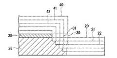
そして、上述した第1エッチングおよび第2エッチングを繰り返し実施する。例えば、40秒間の第1エッチングおよび30秒間の第2エッチングを1セットとして、15セット実施する。これにより、図3(a)に示すように、電極層28および接続層38をパターニングするとともに、電極層28の側面を傾斜面に整形する。 Then, the above-described first etching and second etching are repeatedly performed. For example, the first etching for 40 seconds and the second etching for 30 seconds are set as one set, and 15 sets are performed. As a result, as shown in FIG. 3A, the
図6は、エッチングによる形状変化の説明図である。1回目の第1エッチングでは、エッチングマスク層40の開口部に合わせて接続層30が形成される。次の1回目の第2エッチングでは、接続層30の開口部に合わせて電極層21が形成されるとともに、エッチングマスク層41が縮小形成される。2回目の第1エッチングでは、エッチングマスク層41の開口部に合わせて接続層31が形成される。次の2回目の第2エッチングでは、接続層31の開口部に合わせて電極層22が形成されるとともに、エッチングマスク層42が縮小形成される。このように、第1エッチングおよび第2エッチングを繰り返し実施することにより、理論的には電極層28の側面が階段状に整形されることになる。ただし各エッチングの繰り返し数を増加させることにより、また一般に階段の角部および隅部が鈍るため、電極層28の側面はほぼ傾斜面となる。 FIG. 6 is an explanatory diagram of a shape change due to etching. In the first first etching, the
なおエッチング条件を調節することにより、電極層28の側面の傾斜角度を調整することが可能である。具体的には、図5の条件2の範囲内でO2ガスの割合を増加させるほど、電極層の側面の傾斜角度が小さくなる(緩斜面になる)。O2ガスの割合を増加させるほど、レジストのエッチングレートがMoのエッチングレートより高くなるので、エッチングが縦方向より横方向に早く進行するからである。また第2エッチングの処理時間を長くするほど、電極層の側面の傾斜角度が大きくなる(急斜面になる)。Note that the inclination angle of the side surface of the
次に図3(b)に示すように、接続層38にPイオン等をドープする。そして接続層38および電極層28を覆うように、ポリシリコンからなる半導体層14を形成する。半導体層14は、アモルファスシリコンを1100℃程度に加熱し、結晶化することによって形成する。なお高融点のMo材料で電極層28を形成したので、アモルファスシリコンを加熱して半導体層14を形成する際に、電極層28の溶融を防止することができる。さらに、その半導体層14の表面にゲート絶縁膜16を形成し、そのゲート絶縁膜16の表面にゲート電極18を形成する。以上により、本実施形態に係る薄膜トランジスタ10が完成する。 Next, as shown in FIG. 3B, the
ところで、従来技術に係る薄膜トランジスタの製造方法では、レジスト後退法により電極層28をパターニングした後に、電極層28の表面に接続層をパターニングしていた。この場合、電極層28をパターニングするため第1のレジストが必要であり、接続層38をパターニングするため第2のレジストが必要である。すなわち、2回のフォトリソグラフィを実施するため、2枚のフォトマスクが必要になり、製造コストの低減に限界があった。 By the way, in the method of manufacturing a thin film transistor according to the conventional technique, after patterning the
これに対して、本実施形態に係る薄膜トランジスタの製造方法では、接続層38のa−Si材料のエッチングレートが、電極層28のMo材料およびエッチングマスクのレジスト材料のエッチングレートより大きくなる第1エッチングと、Mo材料およびレジスト材料のエッチングレートが、a−Si材料のエッチングレートより大きくなる第2エッチングとを、繰り返し実施することにより、接続層38および電極層28をパターニングするとともに、電極層28の側面を傾斜面に整形する構成とした。
この構成によれば、接続層38および電極層28のパターニングを、一括して実施することが可能になる。そのため、フォトリソグラフィはエッチングマスク層を形成する際に1回だけ行えばよく、1枚のフォトマスクを形成すれば足りる。したがって、フォトマスクの枚数を削減して製造コストを低減することができる。また電極層28の側面が傾斜面に整形されるので、電極層28の表面に形成される半導体層14の段切れを防止することができる。In contrast, in the method of manufacturing the thin film transistor according to the present embodiment, the first etching in which the etching rate of the a-Si material of the
According to this configuration, the
また本実施形態に係る薄膜トランジスタの製造方法では、電極層および接続層を連続成膜し、一括してエッチングを行うことができる。そのため、電極層28の形成後であって接続層38の形成前に基板が大気曝露されることがなく、電極層28と接続層38との界面に異物が入り込むのを防止することができる。これにより、信頼性に優れた薄膜トランジスタを製造することができる。 In the method for manufacturing a thin film transistor according to this embodiment, the electrode layer and the connection layer can be continuously formed, and etching can be performed collectively. Therefore, the substrate is not exposed to the atmosphere after the
なお、上述した電極層28、接続層38またはエッチングマスク層を、本実施形態とは異なる材料で構成する場合でも、接続層38の構成材料のエッチングレートが、電極層28の構成材料およびエッチングマスク層の構成材料のエッチングレートより大きくなる第1エッチングと、電極層28の構成材料およびエッチングマスク層の構成材料のエッチングレートが、接続層38の構成材料のエッチングレートより大きくなる第2エッチングとを、繰り返し実施することにより、本発明を適用することが可能である。 Even when the above-described
なお、電極層28をMo材料に代えてCu材料で形成する場合には、Cu材料の半導体層14への拡散を防止するため、電極層28を覆うバリア層を形成する必要がある。この場合にも、バリア層の構成材料のエッチングレートが、電極層28のCu材料およびエッチングマスクのレジスト材料のエッチングレートより大きくなる第1エッチングと、Cu材料およびレジスト材料のエッチングレートが、バリア層の構成材料のエッチングレートより大きくなる第2エッチングとを、繰り返し実施することにより、本発明を適用することができる。 When the
なお以上には、本発明に係るパターニング方法を、薄膜トランジスタの製造方法に適用した場合を例にして説明した。しかしながら、本発明に係るパターニング方法は、例えば配線層および機能層の積層体の製造方法に適用することも可能である。この場合には、機能層の構成材料のエッチングレートが、配線層の構成材料およびエッチングマスク層の構成材料のエッチングレートより大きくなる第1エッチングと、配線層の構成材料およびエッチングマスク層の構成材料のエッチングレートが、機能層の構成材料のエッチングレートより大きくなる第2エッチングとを、繰り返し実施すればよい。 Note that the case where the patterning method according to the present invention is applied to a method of manufacturing a thin film transistor has been described above as an example. However, the patterning method according to the present invention can also be applied to, for example, a method for manufacturing a laminate of a wiring layer and a functional layer. In this case, the first etching in which the etching rate of the constituent material of the functional layer is larger than the etching rate of the constituent material of the wiring layer and the constituent material of the etching mask layer, and the constituent material of the wiring layer and the constituent material of the etching mask layer The second etching in which the etching rate is larger than the etching rate of the constituent material of the functional layer may be repeated.
(電子機器)
このように、本発明のパターニング方法を使用して様々な半導体装置を形成することができる。その半導体装置を備えた電子機器の例につき、図7を用いて説明する。
図7は、携帯電話の斜視図である。本発明のパターニング方法を使用して形成した半導体装置は、携帯電話300の筐体内部に配置されている。これにより、低コストで信頼性に優れた携帯電話を提供することができる。(Electronics)
As described above, various semiconductor devices can be formed by using the patterning method of the present invention. An example of an electronic device including the semiconductor device will be described with reference to FIGS.
FIG. 7 is a perspective view of the mobile phone. A semiconductor device formed by using the patterning method of the present invention is disposed inside the housing of the
なお上述した半導体装置は、携帯電話以外にも種々の電子機器に適用することができる。例えば、液晶プロジェクタ、マルチメディア対応のパーソナルコンピュータ(PC)およびエンジニアリング・ワークステーション(EWS)、ページャ、ワードプロセッサ、テレビ、ビューファインダ型またはモニタ直視型のビデオテープレコーダ、電子手帳、電子卓上計算機、カーナビゲーション装置、POS端末、タッチパネルを備えた装置などの電子機器に適用することが可能である。いずれの電子機器も、本発明を適用することにより、低コストで信頼性に優れたものになる。 Note that the semiconductor device described above can be applied to various electronic devices other than cellular phones. For example, LCD projectors, multimedia-compatible personal computers (PCs) and engineering workstations (EWS), pagers, word processors, TVs, viewfinder type or monitor direct view type video tape recorders, electronic notebooks, electronic desk calculators, car navigation systems The present invention can be applied to electronic devices such as a device, a POS terminal, and a device provided with a touch panel. Any electronic device is excellent in reliability at low cost by applying the present invention.
10‥薄膜トランジスタ 14‥半導体層 20,28‥電極層(金属層) 30,38‥オーミック接続層(機能層) 40‥エッチングマスク層 52‥エッチング処理室 DESCRIPTION OF
Claims (6)
Translated fromJapanese前記機能層の表面の所定位置にエッチングマスク層を形成する工程と、
前記機能層の構成材料のエッチングレートが、前記金属層の構成材料および前記エッチングマスク層の構成材料のエッチングレートより大きくなる第1エッチングと、前記金属層の構成材料および前記エッチングマスク層の構成材料のエッチングレートが、前記機能層の構成材料のエッチングレートより大きくなる第2エッチングとを、繰り返し実施することにより、前記機能層および前記金属層をパターニングするとともに、前記金属層の側面を傾斜面とする工程と、
を有することを特徴とするパターニング方法。A step of sequentially laminating a metal layer and a functional layer;
Forming an etching mask layer at a predetermined position on the surface of the functional layer;
The first etching in which the etching rate of the constituent material of the functional layer is higher than the etching rate of the constituent material of the metal layer and the constituent material of the etching mask layer, and the constituent material of the metal layer and the constituent material of the etching mask layer And the second etching in which the etching rate of the functional layer is higher than the etching rate of the constituent material of the functional layer, the functional layer and the metal layer are patterned, and the side surface of the metal layer is inclined. And a process of
A patterning method characterized by comprising:
Priority Applications (1)
| Application Number | Priority Date | Filing Date | Title |
|---|---|---|---|
| JP2005284472AJP2007096053A (en) | 2005-09-29 | 2005-09-29 | Patterning method and thin film transistor manufacturing method |
Applications Claiming Priority (1)
| Application Number | Priority Date | Filing Date | Title |
|---|---|---|---|
| JP2005284472AJP2007096053A (en) | 2005-09-29 | 2005-09-29 | Patterning method and thin film transistor manufacturing method |
Publications (1)
| Publication Number | Publication Date |
|---|---|
| JP2007096053Atrue JP2007096053A (en) | 2007-04-12 |
Family
ID=37981379
Family Applications (1)
| Application Number | Title | Priority Date | Filing Date |
|---|---|---|---|
| JP2005284472AWithdrawnJP2007096053A (en) | 2005-09-29 | 2005-09-29 | Patterning method and thin film transistor manufacturing method |
Country Status (1)
| Country | Link |
|---|---|
| JP (1) | JP2007096053A (en) |
Cited By (1)
| Publication number | Priority date | Publication date | Assignee | Title |
|---|---|---|---|---|
| JP2011192973A (en)* | 2010-02-19 | 2011-09-29 | Semiconductor Energy Lab Co Ltd | Transistor and method of manufacturing the same |
- 2005
- 2005-09-29JPJP2005284472Apatent/JP2007096053A/ennot_activeWithdrawn
Cited By (3)
| Publication number | Priority date | Publication date | Assignee | Title |
|---|---|---|---|---|
| JP2011192973A (en)* | 2010-02-19 | 2011-09-29 | Semiconductor Energy Lab Co Ltd | Transistor and method of manufacturing the same |
| JP2017163150A (en)* | 2010-02-19 | 2017-09-14 | 株式会社半導体エネルギー研究所 | Method for manufacturing transistor |
| KR101794352B1 (en) | 2010-02-19 | 2017-11-06 | 가부시키가이샤 한도오따이 에네루기 켄큐쇼 | Transistor and manufacturing method of the same |
Similar Documents
| Publication | Publication Date | Title |
|---|---|---|
| TWI453912B (en) | Electronic device including a crystal structure having an active region adjacent to a stress layer and method of forming the same | |
| US7785941B2 (en) | Method of fabricating thin film transistor | |
| JP2007200936A (en) | THIN FILM TRANSISTOR, ITS MANUFACTURING METHOD, AND LIQUID CRYSTAL DISPLAY DEVICE | |
| KR100618361B1 (en) | Interconnections including multi-layer metal film stack for improving corrosion and heat resistances | |
| US20090042402A1 (en) | Method for fabricating semiconductor device | |
| JP3302240B2 (en) | Thin film transistor and method of manufacturing the same | |
| US20100165227A1 (en) | Tft-lcd array substrate and method of manufacturing the same | |
| KR100240880B1 (en) | Method for forming gate electrode of semiconductor device | |
| JP4382375B2 (en) | Thin film transistor manufacturing method | |
| WO2005083795A8 (en) | Method for manufacturing semiconductor device and plasma oxidation method | |
| US7229863B2 (en) | Method for fabricating thin film transistors | |
| US20080105926A1 (en) | Thin film transistor and fabrication method thereof | |
| JP2007096053A (en) | Patterning method and thin film transistor manufacturing method | |
| KR20020035747A (en) | Thin film transistor of bottom-gate type, fabrication method thereof and display device using the same | |
| JP4304374B2 (en) | Top gate type thin film transistor | |
| CN100378929C (en) | Method for manufacturing thin film transistor element | |
| JPH0645606A (en) | Manufacture of thin-film transistor matrix | |
| JP5299245B2 (en) | Method for dry etching insulating film on molybdenum metal film and method for manufacturing thin film transistor panel | |
| JP3613221B2 (en) | Thin film transistor manufacturing method | |
| JP4495428B2 (en) | Method for forming thin film transistor | |
| KR100774830B1 (en) | Nonsalicide region formation method of semiconductor device | |
| JP2007033786A (en) | Display device | |
| CN100372081C (en) | Switching element of pixel electrode and manufacturing method thereof | |
| JP4485481B2 (en) | Method for manufacturing semiconductor device | |
| WO2018094597A1 (en) | Method for manufacturing tft array substrate and tft array substrate |
Legal Events
| Date | Code | Title | Description |
|---|---|---|---|
| A300 | Withdrawal of application because of no request for examination | Free format text:JAPANESE INTERMEDIATE CODE: A300 Effective date:20081202 |