JP2007088506A - Semiconductor device, method for manufacturing the same, and method for forming interlayer insulating film - Google Patents
Semiconductor device, method for manufacturing the same, and method for forming interlayer insulating filmDownload PDFInfo
- Publication number
- JP2007088506A JP2007088506AJP2006337910AJP2006337910AJP2007088506AJP 2007088506 AJP2007088506 AJP 2007088506AJP 2006337910 AJP2006337910 AJP 2006337910AJP 2006337910 AJP2006337910 AJP 2006337910AJP 2007088506 AJP2007088506 AJP 2007088506A
- Authority
- JP
- Japan
- Prior art keywords
- organic
- adhesion layer
- insulating film
- film
- siloxane
- Prior art date
- Legal status (The legal status is an assumption and is not a legal conclusion. Google has not performed a legal analysis and makes no representation as to the accuracy of the status listed.)
- Pending
Links
Images


Landscapes
- Internal Circuitry In Semiconductor Integrated Circuit Devices (AREA)
- Formation Of Insulating Films (AREA)
Abstract
Translated fromJapaneseDescription
Translated fromJapanese本発明は、比誘電率及び密着性に優れた層間絶縁膜を有する半導体装置及びその製造方法、並びに比誘電率及び密着性に優れた層間絶縁膜の形成方法に関する。 The present invention relates to a semiconductor device having an interlayer insulating film excellent in relative dielectric constant and adhesiveness, a manufacturing method thereof, and a method of forming an interlayer insulating film excellent in relative dielectric constant and adhesiveness.
半導体集積回路の高集積化の進展に伴い、金属配線同士の間の寄生容量である配線間容量の増加に起因する配線遅延時間の増大が半導体集積回路の高性能化の妨げとなっている。配線遅延時間は金属配線の抵抗と配線間容量との積に比例するいわゆるRC遅延といわれるものである。 With the progress of higher integration of semiconductor integrated circuits, an increase in wiring delay time due to an increase in inter-wire capacitance, which is a parasitic capacitance between metal wirings, has hindered performance enhancement of semiconductor integrated circuits. The wiring delay time is a so-called RC delay that is proportional to the product of the resistance of the metal wiring and the capacitance between the wirings.
従って、配線遅延時間を低減するためには、金属配線の抵抗を小さくするか又は配線間容量を小さくすることが必要である。 Therefore, in order to reduce the wiring delay time, it is necessary to reduce the resistance of the metal wiring or to reduce the capacitance between the wirings.
配線間容量を小さくする方法としては、金属配線同士の間に形成される層間絶縁膜の比誘電率を小さくすることが考えられ、層間絶縁膜として従来のシリコン酸化膜とは異なる材料を用いることが検討されている。 As a method of reducing the capacitance between wirings, it is conceivable to reduce the relative dielectric constant of an interlayer insulating film formed between metal wirings, and a material different from that of a conventional silicon oxide film is used as an interlayer insulating film. Is being considered.
0.25μmの最小加工寸法を有する半導体集積回路では、層間絶縁膜としてシリコン酸化膜にフッ素が添加されてなるフッ素添加シリコン酸化膜が用いられつつある。フッ素添加シリコン酸化膜の比誘電率は、3.3〜3.9程度であって、従来のシリコン酸化膜の4.2〜4.5に比べて小さいので、配線間容量の低減ひいては配線遅延時間の低減に効果的であると報告されている。 In a semiconductor integrated circuit having a minimum processing dimension of 0.25 μm, a fluorine-added silicon oxide film obtained by adding fluorine to a silicon oxide film is being used as an interlayer insulating film. The relative dielectric constant of the fluorine-added silicon oxide film is about 3.3 to 3.9, which is smaller than 4.2 to 4.5 of the conventional silicon oxide film. It has been reported to be effective in reducing time.
ところが、半導体集積回路の微細化がさらに進展することは明らかであり、最小加工寸法が0.13μm以下の半導体集積回路では、比誘電率が2.50以下の層間絶縁膜を用いることが、実用的な処理速度を実現するためには必須であると考えられている。 However, it is clear that further miniaturization of semiconductor integrated circuits will progress further. For semiconductor integrated circuits having a minimum processing dimension of 0.13 μm or less, it is practical to use an interlayer insulating film having a relative dielectric constant of 2.50 or less. It is considered indispensable to realize a typical processing speed.
そこで、比誘電率がフッ素添加シリコン酸化膜よりも一層小さい層間絶縁膜として、低誘電率SOG(スピンオングラス)膜、有機膜及び多孔質膜の検討が行われている。 Therefore, studies have been made on a low dielectric constant SOG (spin-on-glass) film, an organic film, and a porous film as an interlayer insulating film having a relative dielectric constant smaller than that of a fluorine-added silicon oxide film.
現在知られている層間絶縁膜を材料物性の観点から検討すると、有機膜は比誘電率が小さく、その中でもパーフルオロカーボンポリマーは比誘電率が最も小さい材料である。パーフルオロカーボンポリマーの比誘電率は最小のもので1.9程度である。 Examining the currently known interlayer insulating film from the viewpoint of material properties, the organic film has a small relative dielectric constant, and perfluorocarbon polymer is the material having the smallest relative dielectric constant. Perfluorocarbon polymer has a minimum dielectric constant of about 1.9.
しかしながら、パーフルオロカーボンポリマーは、炭素−炭素の骨格を有していると共に、骨格形成に関与する結合以外はすべてフッ素で終端されているため、非常に密着性が悪い。その理由は、パーフルオロカーボンポリマーにおいては、炭素−フッ素結合の分極が小さいため、炭素−フッ素結合は、化学反応性が低くて他の材料との相互作用が小さいので、他の材料との接着が起こりにくいためである。 However, since the perfluorocarbon polymer has a carbon-carbon skeleton and is terminated with fluorine except for the bonds involved in the skeleton formation, the perfluorocarbon polymer has very poor adhesion. The reason for this is that, in the perfluorocarbon polymer, since the polarization of the carbon-fluorine bond is small, the carbon-fluorine bond has low chemical reactivity and has little interaction with other materials. This is because it is difficult to occur.
パーフルオロカーボンポリマー膜を形成する代表的な方法としては、プラズマCVD法が報告されており、プラズマCVD法により形成されたパーフルオロカーボンポリマー膜は一般的にアモルファスフルオロカーボン(a−CF)膜と呼ばれることが多い。 As a typical method for forming a perfluorocarbon polymer film, a plasma CVD method has been reported, and the perfluorocarbon polymer film formed by the plasma CVD method is generally called an amorphous fluorocarbon (a-CF) film. Many.
ところが、a−CF膜は絶縁膜又は金属膜との密着性が非常に悪いため、a−CF膜と絶縁膜又は金属膜との間に密着層を形成することが不可欠となっており、密着層としては、シリコンリッチ酸化膜とダイアモンドライクカーボン(DLC)膜との積層構造が提案されている。シリコンリッチ酸化膜は下地酸化膜及び金属膜との密着性を有していると共にDLC膜との密着性も有しており、また、DLC膜はa−CF膜との密着性を有している。 However, since the a-CF film has very poor adhesion to the insulating film or metal film, it is indispensable to form an adhesion layer between the a-CF film and the insulating film or metal film. As a layer, a laminated structure of a silicon rich oxide film and a diamond like carbon (DLC) film has been proposed. The silicon-rich oxide film has adhesion with the base oxide film and the metal film and also has adhesion with the DLC film, and the DLC film has adhesion with the a-CF film. Yes.
以下、従来の配線構造及びその形成方法について図7を参照しながら説明する。まず、半導体基板10の上に金属配線パターン11を形成した後、金属配線パターン11の上を含む半導体基板10の上に全面に亘って、第1の密着層として、30nmの膜厚の第1のシリコンリッチ酸化膜12及び30nmの膜厚の第1のDLC膜13を順次堆積する。 Hereinafter, a conventional wiring structure and a method for forming the same will be described with reference to FIG. First, after the
次に、第1のDLC膜13の上に200nmの膜厚を有するa−CF膜14を金属配線パターン11同士の間に充填されるように堆積した後、a−CF膜14の上に全面に亘って、第2の密着層として、30nmの膜厚の第2のシリコンリッチ酸化膜15及び30nmの膜厚の第2のDLC膜16を順次堆積する。 Next, an a-CF film 14 having a thickness of 200 nm is deposited on the
しかしながら、第1及び第2のシリコンリッチ酸化膜12、15の比誘電率は3.9以上であり、第1及び第2のDLC膜13、16の比誘電率は2.8以上であって、これらの比誘電率はa−CF膜14の比誘電率に比べてかなり高い。このため、金属配線パターン11同士の間に、比誘電率の高い第1のシリコンリッチ酸化膜12及び第1のDLC膜13からなる第1の密着層が介在するので、金属配線パターン11同士の間の絶縁膜の実効的な比誘電率が増大してしまうという問題がある。例えば、金属配線パターン11同士の間隔が250nmのときに、金属配線パターン11同士の間に、30nmの膜厚の第1のシリコンリッチ酸化膜12と30nmの膜厚の第1のDLC膜13とからなる第1の密着層が介在する場合には、金属配線パターン11同士の間に120nmの膜厚の比誘電率の高い密着層が介在することになるので、金属配線パターン11同士の間の絶縁膜の実効的な比誘電率の増大は大きな問題になる。 However, the relative permittivity of the first and second silicon-
また、反応系が大きく異なる、第1及び第2のシリコンリッチ酸化膜12、15、第1及び第2のDLC膜13、16並びにa−CF膜14をCVD装置の同一の処理室内で形成する場合には、処理室内の雰囲気が激変してしまうので、成膜のプロセスが安定しない。このため、第1及び第2のシリコンリッチ酸化膜12、15、第1及び第2のDLC膜13、16並びにa−CF膜14の各膜質が変化するので、密着性が安定しないという問題がある。 Further, the first and second silicon-
また、第1及び第2のシリコンリッチ酸化膜12、15、第1及び第2のDLC膜13、16並びにa−CF膜14を同一の処理室内で形成する場合には、有機物と酸化物との混合物が処理室の内壁に堆積し、堆積した混合物がシリコンリッチ酸化膜を堆積する際に用いられる酸素によって処理室の内壁から剥がされるので、パーティクルが発生するという問題がある。 When the first and second silicon-
また、酸化膜と有機膜という性質が大きく異なる膜を薄い膜厚で積層する必要があるので、プロセスの制御が困難であるという問題がある。 In addition, there is a problem that it is difficult to control the process because films having greatly different properties such as an oxide film and an organic film need to be stacked with a thin film thickness.
本発明は、前記の問題点を一挙に解決し、金属配線同士の間の絶縁膜の実効的な比誘電率を低減すると共に、金属配線と有機絶縁膜との密着性を向上させることを第1の目的とし、処理室内に発生するパーティクルを低減すると共にプロセスの制御を容易にすることを第2の目的とする。 The present invention solves the above problems all at once, reduces the effective relative dielectric constant of the insulating film between the metal wirings, and improves the adhesion between the metal wiring and the organic insulating film. A first object is to reduce particles generated in the processing chamber and to facilitate process control.
前記の第1の目的を達成するため、本発明に係る第1の半導体装置は、半導体基板上に形成された金属配線パターンと、金属配線パターンの上を含む半導体基板上に形成され、フッ素−炭素結合を含有する有機化合物及び有機シラン誘導体を主原料とするシロキサン含有フッ素化有機膜からなる第1の密着層と、第1の密着層の上に形成され、フッ素−炭素結合を含有する有機化合物を主原料とするフッ素化有機膜からなる有機絶縁膜と、有機絶縁膜の上に形成され、フッ素−炭素結合を含有する有機化合物及び有機シラン誘導体を主原料とするシロキサン含有フッ素化有機膜からなる第2の密着層と、第1の密着層の上に形成された無機化合物からなる無機絶縁膜とを備えている。 In order to achieve the first object, a first semiconductor device according to the present invention is formed on a semiconductor substrate including a metal wiring pattern formed on the semiconductor substrate and the metal wiring pattern. A first adhesion layer made of a siloxane-containing fluorinated organic film mainly composed of an organic compound containing a carbon bond and an organic silane derivative, and an organic containing a fluorine-carbon bond formed on the first adhesion layer An organic insulating film composed of a fluorinated organic film containing a compound as a main material, and a siloxane-containing fluorinated organic film formed on the organic insulating film and containing as a main material an organic compound containing a fluorine-carbon bond and an organic silane derivative And an inorganic insulating film made of an inorganic compound formed on the first adhesion layer.
前記の第1の目的を達成するため、本発明に係る第2の半導体装置は、半導体基板上に形成され、フッ素−炭素結合を含有する有機化合物及び有機シラン誘導体を主原料とするシロキサン含有フッ素化有機膜からなる第1の密着層と、第1の密着層の上に形成され、フッ素−炭素結合を含有する有機化合物を主原料とするフッ素化有機膜からなる有機絶縁膜と、有機絶縁膜に形成された配線溝と、配線溝の側壁に形成され、フッ素−炭素結合を含有する有機化合物及び有機シラン誘導体を主原料とするシロキサン含有フッ素化有機膜からなる第2の密着層と、配線溝の内部における第1の密着層及び第2の密着層で囲まれた部分に埋め込まれた金属配線とを備えている。 In order to achieve the first object, a second semiconductor device according to the present invention is a siloxane-containing fluorine which is formed on a semiconductor substrate and mainly comprises an organic compound containing a fluorine-carbon bond and an organic silane derivative. A first adhesion layer made of a fluorinated organic film, an organic insulating film formed on the first adhesion layer and made of an organic compound containing a fluorine-carbon bond as a main material, and an organic insulation A wiring groove formed in the film, a second adhesion layer formed on a sidewall of the wiring groove, and comprising a siloxane-containing fluorinated organic film mainly composed of an organic compound containing a fluorine-carbon bond and an organic silane derivative; And a metal wiring embedded in a portion surrounded by the first adhesion layer and the second adhesion layer inside the wiring groove.
前記の第1の目的を達成するため、本発明に係る第3の半導体装置は、半導体基板上に形成され、フッ素−炭素結合を含有する有機化合物及び有機シラン誘導体を主原料とするシロキサン含有フッ素化有機膜からなる第1の密着層と、第1の密着層の上に形成され、フッ素−炭素結合を含有する有機化合物を主原料とするフッ素化有機膜からなる有機絶縁膜と、第1の密着層及び有機絶縁膜に形成され、互いに連通している接続孔及び配線溝と、接続孔及び配線溝の側壁に形成され、フッ素−炭素結合を含有する有機化合物及び有機シラン誘導体を主原料とするシロキサン含有フッ素化有機膜からなる第2の密着層と、接続孔及び配線溝の内部における第2の密着層で囲まれた部分に埋め込まれた金属膜からなるコンタクト及び金属配線とを備えている。 In order to achieve the first object, a third semiconductor device according to the present invention is a siloxane-containing fluorine which is formed on a semiconductor substrate and mainly contains an organic compound containing a fluorine-carbon bond and an organic silane derivative. A first adhesion layer made of a fluorinated organic film, an organic insulating film formed on the first adhesion layer and made of an organic compound containing a fluorine-carbon bond as a main material, and a first The main raw material is an organic compound and an organic silane derivative containing a fluorine-carbon bond, formed in a contact hole and a wiring groove which are formed in the adhesion layer and the organic insulating film, and are formed on the side walls of the connection hole and the wiring groove. A second adhesion layer made of a siloxane-containing fluorinated organic film, and a contact and metal wiring made of a metal film embedded in a portion surrounded by the second adhesion layer inside the connection hole and the wiring groove. Eteiru.
前記の第1の目的を達成するため、本発明に係る第4の半導体装置は、半導体基板上に形成され、フッ素−炭素結合を含有する有機化合物及び有機シラン誘導体を主原料とするシロキサン含有フッ素化有機膜からなる第1の密着層と、第1の密着層の上に形成された無機化合物からなる第1の無機絶縁膜と、第1の無機絶縁膜の上に形成され、フッ素−炭素結合を含有する有機化合物及び有機シラン誘導体を主原料とするシロキサン含有フッ素化有機膜からなる第2の密着層と、第2の密着層の上に形成され、フッ素−炭素結合を含有する有機化合物を主原料とするフッ素化有機膜からなる第1の有機絶縁膜と、第1の有機絶縁膜の上に形成され、フッ素−炭素結合を含有する有機化合物及び有機シラン誘導体を主原料とするシロキサン含有フッ素化有機膜からなる第3の密着層と、第3の密着層の上に形成された無機化合物からなる第2の無機絶縁膜と、第2の無機絶縁膜の上に形成され、フッ素−炭素結合を含有する有機化合物及び有機シラン誘導体を主原料とするシロキサン含有フッ素化有機膜からなる第4の密着層と、第4の密着層の上に形成され、フッ素−炭素結合を含有する有機化合物を主原料とするフッ素化有機膜からなる第2の有機絶縁膜と、第2の有機絶縁膜の上に形成され、フッ素−炭素結合を含有する有機化合物及び有機シラン誘導体を主原料とするシロキサン含有フッ素化有機膜からなる第5の密着層と、第5の密着層の上に形成された無機化合物からなる第3の無機絶縁膜と、第1の密着層、第1の無機絶縁膜、第2の密着層、第1の有機絶縁膜、第3の密着層、第2の無機絶縁膜、第4の密着層、第2の有機絶縁膜、第5の密着層及び第3の無機絶縁膜からなる層間絶縁膜に形成され、互いに連通している接続孔及び配線溝と、接続孔及び配線溝の側壁に形成され、フッ素−炭素結合を含有する有機化合物及び有機シラン誘導体を主原料とするシロキサン含有フッ素化有機膜からなる第6の密着層と、接続孔及び配線溝の内部における第6の密着層で囲まれた部分に埋め込まれた金属膜からなるコンタクト及び金属配線とを備えている。 In order to achieve the first object, a fourth semiconductor device according to the present invention is a siloxane-containing fluorine which is formed on a semiconductor substrate and mainly comprises an organic compound containing a fluorine-carbon bond and an organic silane derivative. A first adhesion layer made of a fluorinated organic film; a first inorganic insulation film made of an inorganic compound formed on the first adhesion layer; and a fluorine-carbon film formed on the first inorganic insulation film. A second adhesion layer comprising a siloxane-containing fluorinated organic film comprising a bond-containing organic compound and an organic silane derivative as a main raw material, and an organic compound containing a fluorine-carbon bond formed on the second adhesion layer A first organic insulating film made of a fluorinated organic film mainly composed of silane, and a siloxane formed on the first organic insulating film and mainly composed of an organic compound containing a fluorine-carbon bond and an organic silane derivative Contains A third adhesion layer made of a fluorinated organic film; a second inorganic insulation film made of an inorganic compound formed on the third adhesion layer; and a second inorganic insulation film formed on the second inorganic insulation film, A fourth adhesion layer composed of a siloxane-containing fluorinated organic film mainly composed of an organic compound containing a carbon bond and an organic silane derivative, and a fluorine-carbon bond formed on the fourth adhesion layer; A second organic insulating film made of a fluorinated organic film containing an organic compound as a main raw material; an organic compound containing a fluorine-carbon bond and an organic silane derivative formed on the second organic insulating film as a main raw material; A fifth adhesion layer made of a siloxane-containing fluorinated organic film, a third inorganic insulating film made of an inorganic compound formed on the fifth adhesion layer, a first adhesion layer, and a first inorganic insulation Film, second adhesion layer, first organic insulating film, third Connection formed in an interlayer insulating film composed of an adhesion layer, a second inorganic insulating film, a fourth adhesion layer, a second organic insulating film, a fifth adhesion layer, and a third inorganic insulating film, and communicating with each other A sixth adhesion layer made of a siloxane-containing fluorinated organic film mainly formed of an organic compound containing a fluorine-carbon bond and an organic silane derivative, formed on the sidewalls of the hole and the wiring groove, and the connection hole and the wiring groove; A contact and a metal wiring made of a metal film embedded in a portion surrounded by a sixth adhesion layer inside the connection hole and the wiring groove are provided.
第1〜第4の半導体装置によると、フッ素−炭素結合を含有する有機化合物及び有機シラン誘導体を主原料とするシロキサン含有フッ素化有機膜からなる密着層の比誘電率は2.5以下であって、従来のシリコンリッチ酸化膜の比誘電率(3.9以上)又はDLC膜の比誘電率(2.8以上)に比べて小さい。 According to the first to fourth semiconductor devices, the relative dielectric constant of the adhesion layer made of the siloxane-containing fluorinated organic film mainly composed of an organic compound containing a fluorine-carbon bond and an organic silane derivative was 2.5 or less. Therefore, it is smaller than the relative dielectric constant (3.9 or higher) of the conventional silicon-rich oxide film or the relative dielectric constant (2.8 or higher) of the DLC film.
フッ素−炭素結合を含有する有機化合物と有機シラン誘導体とは、任意の混合比で、酸化剤非存在下においてプラズマにより共重合してシロキサン含有フッ素化有機膜(有機・無機複合膜)となる。このシロキサン含有フッ素化有機膜においては、有機シラン誘導体のアルコキシ基からシロキサンが形成され、形成されたシロキサンの酸素と金属配線パターン(又は接続孔に埋め込まれたコンタクト又は配線溝に埋め込まれた金属配線)の金属とが強固に結合するため、密着層と金属配線パターン(又はコンタクト又は金属配線)との密着性が高くなる。また、形成されたシロキサンの酸素は無機絶縁膜の無機化合物とも強固に結合するため、密着層と無機絶縁膜との密着性も高くなる。 An organic compound containing a fluorine-carbon bond and an organic silane derivative are copolymerized by plasma in an arbitrary mixing ratio and in the absence of an oxidizing agent to form a siloxane-containing fluorinated organic film (organic / inorganic composite film). In this siloxane-containing fluorinated organic film, siloxane is formed from the alkoxy group of the organosilane derivative, and the formed siloxane oxygen and metal wiring pattern (or contact embedded in the connection hole or metal wiring embedded in the wiring trench) ) Are strongly bonded to each other, and the adhesion between the adhesion layer and the metal wiring pattern (or contact or metal wiring) is increased. Further, since the oxygen of the formed siloxane is strongly bonded to the inorganic compound of the inorganic insulating film, the adhesion between the adhesive layer and the inorganic insulating film is also improved.
密着層を構成する有機シラン誘導体の有機基と有機絶縁膜を構成するフッ素−炭素結合を含有する有機化合物の有機基とが共重合反応して、有機シラン誘導体の有機基が有機化合物の炭素骨格に共有結合するため、密着層と有機絶縁膜との密着性も高くなる。 The organic group of the organic silane derivative composing the adhesion layer and the organic group of the organic compound containing a fluorine-carbon bond composing the organic insulating film undergo a copolymerization reaction, and the organic group of the organic silane derivative becomes the carbon skeleton of the organic compound. Since it is covalently bonded, the adhesion between the adhesion layer and the organic insulating film is increased.
前記の第1及び第2の目的を達成するため、本発明に係る第1の半導体装置の製造方法は、半導体基板上に金属配線パターンを形成する工程と、金属配線パターンの上を含む半導体基板上に、プラズマCVD法により、フッ素−炭素結合を含有する有機化合物及び有機シラン誘導体を主原料とするシロキサン含有フッ素化有機膜からなる第1の密着層を形成する工程と、第1の密着層の上に、プラズマCVD法により、フッ素−炭素結合を含有する有機化合物を主原料とするフッ素化有機膜からなる有機絶縁膜を形成する工程と、有機絶縁膜の上に、プラズマCVD法により、フッ素−炭素結合を含有する有機化合物及び有機シラン誘導体を主原料とするシロキサン含有フッ素化有機膜からなる第2の密着層を形成する工程と、第1の密着層の上に無機化合物からなる無機絶縁膜を形成する工程とを備えている。 In order to achieve the first and second objects, a first method of manufacturing a semiconductor device according to the present invention includes a step of forming a metal wiring pattern on a semiconductor substrate, and a semiconductor substrate including the metal wiring pattern. A step of forming a first adhesion layer comprising a siloxane-containing fluorinated organic film comprising, as a main raw material, an organic compound containing a fluorine-carbon bond and an organic silane derivative by a plasma CVD method; A step of forming an organic insulating film made of a fluorinated organic film mainly composed of an organic compound containing a fluorine-carbon bond by plasma CVD, and on the organic insulating film by plasma CVD, A step of forming a second adhesion layer comprising a siloxane-containing fluorinated organic film mainly composed of an organic compound containing a fluorine-carbon bond and an organic silane derivative, and the first adhesion layer And a step of forming an inorganic insulating film made of an inorganic compound above.
第1の半導体装置の製造方法において、第1の密着層を構成するシロキサン含有フッ素化有機膜の原料となる有機化合物と、有機絶縁膜を構成するフッ素化有機膜の原料なる有機化合物と、第2の密着層を構成するシロキサン含有フッ素化有機膜の原料となる有機化合物とは、同種類の有機化合物であることが好ましい。 In the first method for manufacturing a semiconductor device, an organic compound as a raw material for the siloxane-containing fluorinated organic film constituting the first adhesion layer, an organic compound as a raw material for the fluorinated organic film constituting the organic insulating film, It is preferable that the organic compound which is a raw material of the siloxane-containing fluorinated organic film constituting the two adhesion layers is the same kind of organic compound.
第1の半導体装置の製造方法において、第1の密着層及び第2の密着層を構成するシロキサン含有フッ素化有機膜の原料となる有機シラン誘導体は、R1nSi(OR2)4−n(但し、nは1〜3の整数であり、R1はアルキル基又はアリール基であり、R2はアルキル基又はアリール基である。)の一般式で表される有機シラン誘導体であることが好ましい。In the first method for manufacturing a semiconductor device, the organosilane derivative used as a raw material for the siloxane-containing fluorinated organic film constituting the first adhesion layer and the second adhesion layer is R1n Si (OR2 )4-n. (Where n is an integer of 1 to 3, R1 is an alkyl group or an aryl group, and R2 is an alkyl group or an aryl group), and is an organosilane derivative represented by the general formula: preferable.
前記の第1及び第2の目的を達成するため、本発明に係る第2の半導体装置の製造方法は、半導体基板上に、フッ素−炭素結合を含有する有機化合物及び有機シラン誘導体を主原料とするシロキサン含有フッ素化有機膜からなる第1の密着層を形成する工程と、第1の密着層の上に無機化合物からなる第1の無機絶縁膜を形成する工程と、第1の無機絶縁膜の上に、フッ素−炭素結合を含有する有機化合物及び有機シラン誘導体を主原料とするシロキサン含有フッ素化有機膜からなる第2の密着層を形成する工程と、第2の密着層の上に、フッ素−炭素結合を含有する有機化合物を主原料とするフッ素化有機膜からなる第1の有機絶縁膜を形成する工程と、第1の有機絶縁膜の上に、フッ素−炭素結合を含有する有機化合物及び有機シラン誘導体を主原料とするシロキサン含有フッ素化有機膜からなる第3の密着層を形成する工程と、第3の密着層の上に無機化合物からなる第2の無機絶縁膜を形成する工程と、第2の無機絶縁膜の上に、フッ素−炭素結合を含有する有機化合物及び有機シラン誘導体を主原料とするシロキサン含有フッ素化有機膜からなる第4の密着層を形成する工程と、第4の密着層の上にフッ素−炭素結合を含有する有機化合物を主原料とするフッ素化有機膜からなる第2の有機絶縁膜を形成する工程と、第2の有機絶縁膜の上に、フッ素−炭素結合を含有する有機化合物及び有機シラン誘導体を主原料とするシロキサン含有フッ素化有機膜からなる第5の密着層を形成する工程と、第5の密着層の上に無機化合物からなる第3の無機絶縁膜を形成する工程と、第1の密着層、第1の無機絶縁膜、第2の密着層、第1の有機絶縁膜、第3の密着層、第2の無機絶縁膜、第4の密着層、第2の有機絶縁膜、第5の密着層及び第3の無機絶縁膜からなる層間絶縁膜に、互いに連通する接続孔及び配線溝を形成する工程と、接続孔及び配線溝の側壁に、フッ素−炭素結合を含有する有機化合物及び有機シラン誘導体を主原料とするシロキサン含有フッ素化有機膜からなる第6の密着層を形成する工程と、接続孔及び配線溝の内部における第6の密着層で囲まれた部分に金属膜を埋め込んで、該金属膜からなるコンタクト及び金属配線を形成する工程と備えている。 In order to achieve the first and second objects described above, a second method of manufacturing a semiconductor device according to the present invention includes an organic compound containing a fluorine-carbon bond and an organic silane derivative as a main raw material on a semiconductor substrate. Forming a first adhesion layer made of a siloxane-containing fluorinated organic film, forming a first inorganic insulation film made of an inorganic compound on the first adhesion layer, and a first inorganic insulation film A step of forming a second adhesion layer composed of a siloxane-containing fluorinated organic film mainly composed of an organic compound containing a fluorine-carbon bond and an organic silane derivative, and on the second adhesion layer, A step of forming a first organic insulating film made of a fluorinated organic film mainly containing an organic compound containing a fluorine-carbon bond, and an organic containing a fluorine-carbon bond on the first organic insulating film Compounds and organosilane derivatives Forming a third adhesion layer made of a siloxane-containing fluorinated organic film mainly composed of a body, forming a second inorganic insulating film made of an inorganic compound on the third adhesion layer, Forming a fourth adhesion layer comprising a siloxane-containing fluorinated organic film mainly composed of an organic compound containing a fluorine-carbon bond and an organic silane derivative on the inorganic insulating film, and a fourth adhesion Forming a second organic insulating film made of a fluorinated organic film mainly composed of an organic compound containing a fluorine-carbon bond on the layer, and a fluorine-carbon bond on the second organic insulating film Forming a fifth adhesion layer made of a siloxane-containing fluorinated organic film mainly containing an organic compound containing silane and an organic silane derivative, and a third inorganic insulation made of an inorganic compound on the fifth adhesion layer Forming a film and 1st adhesion layer, 1st inorganic insulating film, 2nd adhesion layer, 1st organic insulation film, 3rd adhesion layer, 2nd inorganic insulation film, 4th adhesion layer, 2nd organic insulation Forming a connection hole and a wiring groove communicating with each other in an interlayer insulating film composed of the film, the fifth adhesion layer, and the third inorganic insulating film, and containing a fluorine-carbon bond on the side wall of the connection hole and the wiring groove Forming a sixth adhesion layer made of a siloxane-containing fluorinated organic film mainly composed of an organic compound and an organic silane derivative, and a portion surrounded by the sixth adhesion layer inside the connection hole and the wiring groove A step of embedding a metal film to form a contact and metal wiring made of the metal film.
第1及び第2の半導体装置の製造方法によると、フッ素−炭素結合を含有する有機化合物と有機シラン誘導体とを主原料とするシロキサン含有フッ素化有機膜からなる密着層の比誘電率は2.5以下であって、従来のシリコンリッチ酸化膜の比誘電率(3.9以上)又はDLC膜の比誘電率(2.8以上)に比べて小さい。 According to the first and second methods for manufacturing a semiconductor device, the relative dielectric constant of the adhesion layer made of a siloxane-containing fluorinated organic film mainly composed of an organic compound containing a fluorine-carbon bond and an organic silane derivative is 2. 5 or less, which is smaller than the relative dielectric constant (3.9 or more) of the conventional silicon-rich oxide film or the relative dielectric constant (2.8 or more) of the DLC film.
フッ素−炭素結合を含有する有機化合物と有機シラン誘導体とは、任意の混合比で、酸化剤非存在下においてプラズマにより共重合してシロキサン含有フッ素化有機膜(有機・無機複合膜)となる。このシロキサン含有フッ素化有機膜においては、有機シラン誘導体のアルコキシ基からシロキサンが形成され、形成されたシロキサンの酸素と金属配線パターン(又は接続孔に埋め込まれたコンタクト又は配線溝に埋め込まれた金属配線)の金属とが強固に結合するため、密着層と金属配線パターン(又はコンタクト又は金属配線)との密着性が高くなる。また、形成されたシロキサンの酸素は無機絶縁膜の無機化合物とも強固に結合するため、密着層と無機絶縁膜との密着性も高くなる。 An organic compound containing a fluorine-carbon bond and an organic silane derivative are copolymerized by plasma in an arbitrary mixing ratio and in the absence of an oxidizing agent to form a siloxane-containing fluorinated organic film (organic / inorganic composite film). In this siloxane-containing fluorinated organic film, siloxane is formed from the alkoxy group of the organosilane derivative, and the formed siloxane oxygen and metal wiring pattern (or contact embedded in the connection hole or metal wiring embedded in the wiring trench) ) Are strongly bonded to each other, and the adhesion between the adhesion layer and the metal wiring pattern (or contact or metal wiring) is increased. Further, since the oxygen of the formed siloxane is strongly bonded to the inorganic compound of the inorganic insulating film, the adhesion between the adhesive layer and the inorganic insulating film is also improved.
密着層を構成する有機シラン誘導体の有機基と有機絶縁膜を構成するフッ素−炭素結合を含有する有機化合物の有機基とが共重合反応して、有機シラン誘導体の有機基が有機化合物の炭素骨格に共有結合するため、密着層と有機絶縁膜との密着性も高くなる。 The organic group of the organic silane derivative composing the adhesion layer and the organic group of the organic compound containing a fluorine-carbon bond composing the organic insulating film undergo a copolymerization reaction, and the organic group of the organic silane derivative becomes the carbon skeleton of the organic compound. Since it is covalently bonded, the adhesion between the adhesion layer and the organic insulating film is increased.
また、フッ素−炭素結合を含有する有機化合物を主原料とするフッ素化有機膜からなる有機絶縁膜を形成する工程は、フッ素−炭素結合を含有する有機化合物及び有機シラン誘導体を主原料とするシロキサン含有フッ素化有機膜からなる密着層を形成する工程同士の間に行なわれると共に、有機絶縁膜の形成工程と密着層の形成工程とは同一の反応系プロセスであるため、有機絶縁膜の形成工程とその前後の密着層の形成工程とを連続して行なうことができると共に、反応系のプロセスの制御が容易である上に、処理室の雰囲気を一定に保つことができる。 In addition, the step of forming an organic insulating film composed of a fluorinated organic film mainly containing an organic compound containing a fluorine-carbon bond is a siloxane mainly containing an organic compound containing a fluorine-carbon bond and an organic silane derivative. The organic insulating film forming step is performed between the steps of forming the adhesive layer made of the fluorinated organic film, and the organic insulating film forming step and the adhesive layer forming step are the same reaction process. And the process of forming the adhesion layer before and after that can be performed continuously, the process of the reaction system can be easily controlled, and the atmosphere in the processing chamber can be kept constant.
本発明に係る第1の層間絶縁膜の形成方法は、半導体基板上に順次堆積された、第1の密着層、有機絶縁膜及び第2の密着層からなる層間絶縁膜の形成方法を対象とし、半導体基板が保持されている処理室内に、フッ素−炭素結合を含有する有機化合物を含む第1の原料ガス及び有機シラン誘導体を含む第2の原料ガスを導入した後、第1の原料ガスの導入量をほぼ一定に保つ一方、第2の原料ガスの導入量を減少させながら、第1の原料ガス及び第2の原料ガスからなるプラズマにより、半導体基板上にシロキサン含有フッ素化有機膜からなる第1の密着層を形成する工程と、処理室内に第1の原料ガスをその導入量をほぼ一定に保ちながら導入する一方、第2の原料ガスの導入を停止して、第1の原料ガスからなるプラズマにより、第1の密着層の上にフッ素−炭素結合を含有する有機化合物からなる有機絶縁膜を形成する工程と、処理室内に、第1の原料ガスをその導入量をほぼ一定に保ちながら導入すると共に、第2の原料ガスを再び導入し且つ第2の原料ガスの導入量を増加させながら、第1の原料ガス及び第2の原料ガスからなるプラズマにより、有機絶縁膜の上にシロキサン含有フッ素化有機膜からなる第2の密着層を形成する工程とを備えている。 The method for forming a first interlayer insulating film according to the present invention is directed to a method for forming an interlayer insulating film comprising a first adhesion layer, an organic insulating film, and a second adhesion layer sequentially deposited on a semiconductor substrate. After introducing the first source gas containing an organic compound containing a fluorine-carbon bond and the second source gas containing an organosilane derivative into the processing chamber in which the semiconductor substrate is held, While the introduction amount is kept substantially constant, the siloxane-containing fluorinated organic film is formed on the semiconductor substrate by the plasma comprising the first source gas and the second source gas while reducing the introduction amount of the second source gas. The step of forming the first adhesion layer and the first raw material gas are introduced into the processing chamber while maintaining the introduction amount thereof substantially constant, while the introduction of the second raw material gas is stopped and the first raw material gas is introduced. The plasma comprising A step of forming an organic insulating film made of an organic compound containing a fluorine-carbon bond on the adhesion layer; a first source gas is introduced into the processing chamber while keeping the introduction amount substantially constant; The siloxane-containing fluorinated organic film is formed on the organic insulating film by plasma composed of the first source gas and the second source gas while introducing the source gas again and increasing the introduction amount of the second source gas. Forming a second adhesion layer.
第1の層間絶縁膜の形成方法によると、処理室内に導入した第1の原料ガスの導入量をほぼ一定に保つ一方、第2の原料ガスの導入量を減少させながら、半導体基板上に第1の密着層を形成した後、処理室内に導入している第1の原料ガスの導入量をほぼ一定に保つ一方、第2の原料ガスの導入を停止して、第1の密着層の上に有機絶縁膜を形成し、その後、処理室内に導入している第1の原料ガスの導入量をほぼ一定に保つ一方、再び導入した第2の原料ガスの導入量を増加させながら、有機絶縁膜の上に第2の密着層を形成するため、つまり、第1の原料ガスの導入量をほぼ一定に保った状態で、第2の原料ガスの導入量を減少、停止及び増加することにより、第1の密着層、有機絶縁膜及び第2の密着層を連続的に形成することができる。 According to the method for forming the first interlayer insulating film, the introduction amount of the first source gas introduced into the processing chamber is kept substantially constant, while the introduction amount of the second source gas is reduced, and the first source gas is introduced onto the semiconductor substrate. After forming the first adhesion layer, the introduction amount of the first source gas introduced into the processing chamber is kept substantially constant, while the introduction of the second source gas is stopped to An organic insulating film is then formed, and then the amount of the first source gas introduced into the processing chamber is kept substantially constant, while the amount of the second source gas introduced again is increased while the organic insulating film is increased. In order to form the second adhesion layer on the film, that is, with the introduction amount of the first source gas kept substantially constant, the introduction amount of the second source gas is reduced, stopped, and increased. The first adhesion layer, the organic insulating film and the second adhesion layer can be continuously formed. .
本発明に係る第2の層間絶縁膜の形成方法は、半導体基板上に順次堆積された、第1の密着層、有機絶縁膜及び第2の密着層からなる層間絶縁膜の形成方法を対象とし、半導体基板が保持されている処理室内に、フッ素−炭素結合を含有する有機化合物を含む第1の原料ガス及び有機シラン誘導体を含む第2の原料ガスを、それぞれの導入量をほぼ一定に保ちながら導入しながら、第1の原料ガス及び第2の原料ガスからなるプラズマにより、半導体基板上にシロキサン含有フッ素化有機膜からなる第1の密着層を形成する工程と、処理室内に第1の原料ガスをその導入量をほぼ一定に保ちながら導入する一方、第2の原料ガスの導入を停止して、第1の原料ガスからなるプラズマにより、第1の密着層の上にフッ素−炭素結合を含有する有機化合物からなる有機絶縁膜を形成する工程と、処理室内に、第1の原料ガスをその導入量をほぼ一定に保ちながら導入すると共に、第2の原料ガスを再び導入し且つ第2の原料ガスの導入量をほぼ一定に保ちながら、第1の原料ガス及び第2の原料ガスからなるプラズマにより、有機絶縁膜の上にシロキサン含有フッ素化有機膜からなる第2の密着層を形成する工程とを備えている。 The second interlayer insulating film forming method according to the present invention is directed to an interlayer insulating film forming method comprising a first adhesion layer, an organic insulating film, and a second adhesion layer, which are sequentially deposited on a semiconductor substrate. The first source gas containing an organic compound containing a fluorine-carbon bond and the second source gas containing an organosilane derivative are kept substantially constant in the processing chamber in which the semiconductor substrate is held. And introducing a first adhesion layer made of a siloxane-containing fluorinated organic film on the semiconductor substrate with plasma made of the first source gas and the second source gas, and a first in the processing chamber. While introducing the source gas while keeping the introduction amount substantially constant, the introduction of the second source gas is stopped, and the fluorine-carbon bond is formed on the first adhesion layer by the plasma made of the first source gas. Containing A step of forming an organic insulating film made of a compound, and a first source gas is introduced into the processing chamber while maintaining the introduction amount thereof substantially constant, and the second source gas is introduced again and the second source gas is introduced. Forming a second adhesion layer composed of a siloxane-containing fluorinated organic film on the organic insulating film by plasma composed of the first source gas and the second source gas while keeping the introduction amount of the gas substantially constant; It has.
第2の層間絶縁膜の形成方法によると、処理室内に、第1の原料ガス及び第2の原料ガスをそれぞれの導入量をほぼ一定に保ちながら、第1の密着層を形成した後、処理室内に導入している第1の原料ガスの導入量をほぼ一定に保つ一方、第2の原料ガスの導入を停止して、第1の密着層の上に有機絶縁膜を形成し、その後、処理室内に導入している第1の原料ガスの導入量をほぼ一定に保つと共に第2の原料ガスを再び導入し且つ第2の原料ガスの導入量をほぼ一定に保ちながら、有機絶縁膜の上に第2の密着層を形成するため、つまり、第1の原料ガスの導入量をほぼ一定に保った状態で、第2の原料ガスの導入、停止及び導入を行なうことにより、第1の密着層、有機絶縁膜及び第2の密着層を連続的に形成することができる。 According to the method for forming the second interlayer insulating film, after forming the first adhesive layer in the processing chamber while maintaining the introduction amounts of the first source gas and the second source gas substantially constant, While maintaining the introduction amount of the first source gas introduced into the room substantially constant, the introduction of the second source gas is stopped to form an organic insulating film on the first adhesion layer, and then While maintaining the introduction amount of the first source gas introduced into the processing chamber substantially constant, introducing the second source gas again and keeping the introduction amount of the second source gas substantially constant, the organic insulating film In order to form the second adhesion layer thereon, that is, by introducing, stopping and introducing the second source gas while maintaining the introduction amount of the first source gas substantially constant, The adhesion layer, the organic insulating film, and the second adhesion layer can be formed continuously.
第1〜第4の半導体装置によると、フッ素−炭素結合を含有する有機化合物及び有機シラン誘導体を主原料とするシロキサン含有フッ素化有機膜からなる密着層の比誘電率は、従来のシリコンリッチ酸化膜とDLC膜との積層膜からなる密着層の比誘電率に比べて小さい。 According to the first to fourth semiconductor devices, the dielectric constant of the adhesion layer composed of a siloxane-containing fluorinated organic film mainly composed of an organic compound containing a fluorine-carbon bond and an organic silane derivative is the same as that of a conventional silicon-rich oxide. It is smaller than the relative dielectric constant of the adhesion layer composed of the laminated film of the film and the DLC film.
密着層と金属配線パターン(又はコンタクト又は金属配線)との密着性、密着層と無機絶縁膜との密着性、及び密着層と有機絶縁膜との密着性はいずれも高いので、金属配線パターン(又はコンタクト又は金属配線)、無機絶縁膜及び有機絶縁膜の相互間の密着性の向上を単層の密着層により実現することができる。 Since the adhesion between the adhesion layer and the metal wiring pattern (or contact or metal wiring), the adhesion between the adhesion layer and the inorganic insulating film, and the adhesion between the adhesion layer and the organic insulating film are all high, the metal wiring pattern ( Alternatively, the adhesion between the inorganic insulating film and the organic insulating film can be improved by a single adhesive layer.
従って、第1〜第4の半導体装置によると、金属配線同士の間の絶縁膜の実効的な比誘電率を低減できると共に、金属配線と有機絶縁膜との間の密着性を向上させることができる。 Therefore, according to the first to fourth semiconductor devices, the effective relative dielectric constant of the insulating film between the metal wirings can be reduced, and the adhesion between the metal wiring and the organic insulating film can be improved. it can.
第1及び第2の半導体装置の製造方法によると、密着層の比誘電率を従来のシリコンリッチ酸化膜とDLC膜との積層膜に比べて小さくできると共に、金属配線パターン(又はコンタクト又は金属配線)、無機絶縁膜及び有機絶縁膜の相互間の密着性の向上を単層で且つ1種類の密着層により実現することができる。 According to the first and second semiconductor device manufacturing methods, the relative dielectric constant of the adhesion layer can be reduced as compared with the conventional laminated film of the silicon-rich oxide film and the DLC film, and the metal wiring pattern (or contact or metal wiring). ), An improvement in adhesion between the inorganic insulating film and the organic insulating film can be realized by a single layer and a single type of adhesion layer.
また、有機絶縁膜の形成工程とその前後の密着層の形成工程とを連続的に行なうことができると共に、反応系のプロセスの制御が容易である上に、処理室の雰囲気を一定に保つことができる。 In addition, the process of forming the organic insulating film and the process of forming the adhesion layer before and after that can be performed continuously, the process of the reaction system is easily controlled, and the atmosphere in the processing chamber is kept constant. Can do.
従って、第1及び第2の半導体装置の製造方法によると、金属配線同士の間の絶縁膜の実効的な比誘電率の低減及び金属配線と有機絶縁膜との間の密着性の向上を、処理室内にパーティクルを発生させることなく且つプロセスの制御性を容易に実現することができる。 Therefore, according to the first and second semiconductor device manufacturing methods, the effective relative dielectric constant of the insulating film between the metal wirings can be reduced and the adhesion between the metal wiring and the organic insulating film can be improved. The process controllability can be easily realized without generating particles in the processing chamber.
第1の半導体装置の製造方法において、第1の密着層の原料となる有機化合物、有機絶縁膜の原料なる有機化合物及び第2の密着層の原料となる有機化合物が同種類の有機化合物であると、プロセスの制御性が一層向上する。 In the first method for manufacturing a semiconductor device, the organic compound that is the raw material of the first adhesion layer, the organic compound that is the raw material of the organic insulating film, and the organic compound that is the raw material of the second adhesion layer are the same kind of organic compound. And process controllability is further improved.
第1の半導体装置の製造方法において、第1の密着層及び第2の密着層の原料が、R1nSi(OR2)4−n(但し、nは1〜3の整数であり、R1はアルキル基又はアリール基であり、R2はアルキル基又はアリール基である。)の一般式で表される有機シラン誘導体であると、密着層の比誘電率を確実に小さくできると共に密着性を確実に向上することができる。In the first method for manufacturing a semiconductor device, the raw materials of the first adhesion layer and the second adhesion layer are R1n Si (OR2 )4-n (where n is an integer of 1 to 3,1 is an alkyl group or an aryl group, and R2 is an alkyl group or an aryl group.) When the organic silane derivative is represented by the general formula: Can be reliably improved.
第1の層間絶縁膜の形成方法によると、第1の原料ガスの導入量をほぼ一定に保った状態で、第2の原料ガスの導入量を減少、停止及び増加することにより、第1の密着層、有機絶縁膜及び第2の密着層を連続的に形成できるため、第1の密着層、有機絶縁膜及び第2の密着層の組成が連続的に変化するので、密着性が非常に高くなる。 According to the first interlayer insulating film forming method, the first source gas introduction amount is decreased, stopped, and increased while the first source gas introduction amount is kept substantially constant. Since the adhesion layer, the organic insulating film, and the second adhesion layer can be continuously formed, the composition of the first adhesion layer, the organic insulating film, and the second adhesion layer is continuously changed. Get higher.
第2の層間絶縁膜の形成方法によると、第1の原料ガスの導入量をほぼ一定に保った状態で、第2の原料ガスの導入、停止及び導入を行なうことにより、第1の密着層、有機絶縁膜及び第2の密着層を連続的に形成できるため、第1及び第2の密着層の膜厚を薄くできるので、層間絶縁膜の実効的な比誘電率を極めて小さくすることができる。 According to the method for forming the second interlayer insulating film, the first adhesion layer is formed by introducing, stopping, and introducing the second source gas while keeping the introduction amount of the first source gas substantially constant. Since the organic insulating film and the second adhesion layer can be formed continuously, the thickness of the first and second adhesion layers can be reduced, so that the effective relative dielectric constant of the interlayer insulation film can be made extremely small. it can.
(第1の実施形態)
以下、本発明の第1の実施形態に係る半導体装置及びその製造方法について、図1(a)〜(c)及び図2(a)〜(c)を参照しながら説明する。(First embodiment)
Hereinafter, a semiconductor device and a manufacturing method thereof according to a first embodiment of the present invention will be described with reference to FIGS. 1 (a) to (c) and FIGS. 2 (a) to (c).
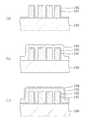
まず、図1(a)に示すように、半導体基板100の上に、例えば高さが800nmで配線スペースが250nmの金属配線パターン101を形成した後、金属配線パターン101の上を含む半導体基板100の上に全面に亘って、例えば20nmの膜厚を有するシロキサン含有フッ素化有機膜からなる第1の密着層102を堆積する。シロキサン含有フッ素化有機膜の堆積方法としては、フッ素−炭素結合を有する有機化合物及び有機シラン誘導体を主原料とする第1の原料ガス、例えばC4F8/CH4/ビニルトリメトキシシラン(vinyltrimethoxysilane)の混合ガスを用いるプラズマCVD法が挙げられ、堆積条件としては、例えばRFパワーは200W、プロセス圧力は200mmTorr、堆積時間は4秒間である。First, as shown in FIG. 1A, after a
次に、図1(b)に示すように、第1の密着層102の上に全面に亘って、例えば200nmの膜厚を有するフッ素化アモルファスカーボン膜からなる有機絶縁膜103を金属配線パターン101同士の間のスペース部が完全に充填されるように堆積する。フッ素化アモルファスカーボン膜の堆積方法としては、フッ素−炭素結合を有する有機化合物を主原料とする第2の原料ガス、例えばC4F8/CH4の混合ガスを用いるプラズマCVD法が挙げられ、堆積条件としては、例えばRFパワーは200W、プロセス圧力は200mmTorr、堆積時間は60秒間である。Next, as shown in FIG. 1B, an organic
次に、図1(c)に示すように、有機絶縁膜103の上に全面に亘って、例えば20nmの膜厚を有するシロキサン含有フッ素化有機膜からなる第2の密着層104を堆積する。シロキサン含有フッ素化有機膜の堆積方法としては、第1の密着層102の場合と同様、フッ素−炭素結合を有する有機化合物及び有機シラン誘導体を主原料とする第1の原料ガス、例えばC4F8/CH4/ビニルトリメトキシシランの混合ガスを用いるプラズマCVD法が挙げられ、堆積条件としては、例えばRFパワーは200W、プロセス圧力は200mmTorr、堆積時間は4秒間である。Next, as shown in FIG. 1C, a
次に、図2(a)に示すように、第2の密着層104の上に全面に亘って例えば50nmの膜厚を有するシリコン酸化膜からなる無機絶縁膜105を堆積した後、該無機絶縁膜105の表面を例えばCMP法により平坦化する。シリコン酸化膜の堆積方法としてはSiH4とN2O との混合ガスを用いるプラズマCVD法が挙げられる。Next, as shown in FIG. 2A, after depositing an inorganic
次に、図2(b)に示すように、第1の密着層102、有機絶縁膜103、第2の密着層104及び無機絶縁膜105に対して選択的にエッチングを行なって接続孔106を形成した後、該接続孔106に例えばタングステンからなる金属膜を埋め込んで金属プラグ107を形成する。尚、無機絶縁膜105としてのシリコン酸化膜105は、接続孔106をドライエッチングにより形成する際のエッチングストッパーとなる。 Next, as illustrated in FIG. 2B, the
第1の実施形態によると、シロキサン含有フッ素化有機膜からなる第1及び第2の密着層102、104の比誘電率は非常に低くて2.5以下であった。 According to the first embodiment, the relative dielectric constant of the first and second adhesion layers 102 and 104 made of the siloxane-containing fluorinated organic film was very low and 2.5 or less.
また、シロキサン含有フッ素化有機膜からなる第1及び第2の密着層102、104とフッ素化アモルファスカーボン膜からなる有機絶縁膜103との密着性は極めて優れており、フッ素化アモルファスカーボンからなる有機膜103の剥離は認められなかった。 Further, the adhesion between the first and second adhesion layers 102 and 104 made of a siloxane-containing fluorinated organic film and the organic insulating
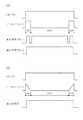
以下、第1の密着層102、有機絶縁膜103及び第2の密着層104を連続的に堆積する際の第1のプロセスシーケンスについて説明する。 Hereinafter, a first process sequence when the
第1のプロセスシーケンスは、堆積条件を例えばRFパワーは200W、プロセス圧力は200mmTorrに保った状態で、フッ素−炭素結合を有する有機化合物及び有機シラン誘導体を主原料とする第1の原料ガスの導入量を一定に保った状態で、フッ素−炭素結合を有する有機化合物を主原料とする第2の原料ガスの導入量をパルス的に変化させる方法である。 The first process sequence is the introduction of a first source gas mainly containing an organic compound having a fluorine-carbon bond and an organosilane derivative while keeping the deposition conditions such as RF power at 200 W and process pressure at 200 mm Torr. This is a method of changing the introduction amount of the second source gas using an organic compound having a fluorine-carbon bond as a main source in a pulsed manner while keeping the amount constant.
第1のプロセスシーケンスについて、図3(a)を参照しながら具体的に説明する。まず、プラズマCVD処理室にC4F8ガス、CH4ガス及びビニルトリメトキシシランガスを導入した直後にプラズマ発生用の高周波電力を印加すると共に、C4F8ガス、CH4ガス及びビニルトリメトキシシランガスを各導入量を一定にして4秒間導入することにより、第1の密着層102を堆積する。次に、ビニルトリメトキシシランガスの導入を停止する一方、C4F8ガス及びCH4ガスを各導入量を一定にして60秒間導入することにより、有機絶縁膜103を堆積する。次に、C4F8ガス及びCH4ガスの各導入量を一定に保ったまま、ビニルトリメトキシシランガスを再び一定量4秒間導入することにより、第2の密着層104を堆積する。プラズマ発生用の高周波電力の印加方法としては、図3(a)においてNo.1で示すように、ビニルトリメトキシシランガスの導入及び停止の各直前及び各直後に僅かな時間だけ停止してもよいし、図3(a)においてNo.2で示すように、ビニルトリメトキシシランガスの導入及び停止とは無関係に継続しておき、C4F8ガス、CH4ガス及びビニルトリメトキシシランガスの導入停止の直前に停止してもよい。The first process sequence will be specifically described with reference to FIG. First, immediately after introducing C4 F8 gas, CH4 gas and vinyltrimethoxysilane gas into the plasma CVD processing chamber, high-frequency power for plasma generation is applied, and C4 F8 gas, CH4 gas and vinyltrimethoxy are applied. The
第1のプロセスシーケンスによると、第1の密着層102及び第2の密着層104の堆積工程においては、ビニルトリメトキシシランガスを一定量づつ導入するため、第1及び第2の密着層102、104におけるシロキサンの含有率は密着層の膜厚方向でほぼ一定となる。 According to the first process sequence, in the step of depositing the
また、第1のプロセスシーケンスによると、C4F8ガス、CH4ガス及びビニルトリメトキシシランガスの導入量を経時的に変化させることなく、バルブの開閉という単純な操作でビニルトリメトキシシランガスの導入及び停止を行なうことができるため、第1及び第2の密着層102、104の膜厚を薄くすることが容易である。このため、金属配線パターン101同士の間の実効的な比誘電率を小さくできるので、容量の増加を抑制することができる。Furthermore, in the first process sequence, C4 F8 gas, without time-varying the introduced amount of CH4 gas and vinyltrimethoxysilane gas, introduction of vinyltrimethoxysilane gas by a simple operation of opening and closing of the valve Since the first and second adhesion layers 102 and 104 can be easily reduced in thickness, the film can be easily stopped. For this reason, since the effective relative dielectric constant between the
もっとも、第1のプロセスシーケンスは、第1又は第2の密着層102、104と有機絶縁膜103との界面において組成が急峻に変化するため、密着性が若干低下するという短所を有している。 However, the first process sequence has a disadvantage that the adhesiveness is slightly lowered because the composition changes sharply at the interface between the first or second adhesion layers 102 and 104 and the organic insulating
以下、第1の密着層102、有機絶縁膜103及び第2の密着層104を連続的に堆積する際の第2のプロセスシーケンスについて説明する。 Hereinafter, a second process sequence when the
第2のプロセスシーケンスは、堆積条件を例えばRFパワーは200W、プロセス圧力は200mmTorrに保った状態で、フッ素−炭素結合を有する有機化合物及び有機シラン誘導体を主原料とする第1の原料ガスの導入量を一定に保つ一方、フッ素−炭素結合を有する有機化合物を主原料とする第2の原料ガスの導入量を連続的に変化させる方法である。 The second process sequence is the introduction of a first source gas mainly containing an organic compound having a fluorine-carbon bond and an organosilane derivative while keeping the deposition conditions, for example, RF power at 200 W and process pressure at 200 mm Torr. In this method, the amount of the second raw material gas introduced using an organic compound having a fluorine-carbon bond as a main raw material is continuously changed while the amount is kept constant.
第2のプロセスシーケンスについて、図3(b)を参照しながら具体的に説明する。まず、プラズマCVD処理室にC4F8ガス、CH4ガス及びビニルトリメトキシシランガスを導入した直後に、プラズマ発生用の高周波電力を印加すると共に、C4F8ガス及びCH4ガスの導入量を一定に保つ一方、ビニルトリメトキシシランガスの導入量を連続的に減少させていき、ビニルトリメトキシシランガスの導入を導入開始から4秒後に停止することにより、第1の密着層102を堆積する。次に、ビニルトリメトキシシランガスの導入を停止したまま、C4F8ガス及びCH4ガスを各導入量を一体にして60秒間導入することにより、有機絶縁膜103を堆積する。次に、C4F8ガス及びCH4ガスの各導入量を一定に保ったまま、ビニルトリメトキシシランガスを再び導入すると共にその導入量を連続的に増加させる状態を4秒間継続することにより、第2の密着層104を堆積する。プラズマ発生用の高周波電力の印加方法としては、図3(b)に示すように、C4F8ガス、CH4ガス及びビニルトリメトキシシランガスの導入直後に開始すると共に、C4F8ガス、CH4ガス及びビニルトリメトキシシランガスの導入停止直前に終了する。The second process sequence will be specifically described with reference to FIG. First, immediately after introducing C4 F8 gas, CH4 gas, and vinyltrimethoxysilane gas into the plasma CVD processing chamber, high frequency power for plasma generation is applied, and the amount of C4 F8 gas and CH4 gas introduced The
第2のプロセスシーケンスによると、ビニルトリメトキシシランガスの導入量を経時的に変化させる必要があるため、第1及び第2の密着層102、104の堆積時間の短縮がやや困難になる。このため、第1のプロセスシーケンスに比べて、第1及び第2の密着層102、104の膜厚が厚くなるので、金属配線パターン101同士の間の実効的な比誘電率が若干大きくなるが、第1及び第2の密着層102、104と有機絶縁膜103との組成変化が連続的であるため、密着性は非常に高くなる。 According to the second process sequence, it is necessary to change the introduction amount of the vinyltrimethoxysilane gas with time, so it is somewhat difficult to shorten the deposition time of the first and second adhesion layers 102 and 104. For this reason, since the film thickness of the first and second adhesion layers 102 and 104 is thicker than that in the first process sequence, the effective relative dielectric constant between the
尚、第1の実施形態においては、第1の密着層102を構成するシロキサン含有フッ素化有機膜の主原料となる有機化合物、有機絶縁膜103を構成するフッ素化アモルファスカーボン膜の主原料となる有機化合物、及び第2の密着層104を構成するシロキサン含有フッ素化有機膜の主原料となる有機化合物としては、C4F8を用いたが、これに代えて、C10F18等のように、一般式:CxFy(xは1〜15の整数、yは4〜32の整数)で表わされるフッ素−炭素結合を有する有機化合物を広く用いることができる。In the first embodiment, an organic compound as a main raw material for the siloxane-containing fluorinated organic film constituting the
また、第1の実施形態においては、有機絶縁膜103を構成するフッ素化アモルファスカーボン膜の主原料となる有機シラン誘導体としては、ビニルトリメトキシシランを用いたが、これに代えて、R1nSi(OR2)4−n(但し、nは1〜3の整数であり、R1はアルキル基又はアリール基であり、R2はアルキル基又はアリール基である。)の一般式で表される有機シラン誘導体を広く用いることができる。In the first embodiment, vinyltrimethoxysilane is used as the organic silane derivative that is the main raw material of the fluorinated amorphous carbon film constituting the organic insulating
(第2の実施形態)
以下、本発明の第2の実施形態に係る配線構造及びその形成方法について、図4(a)、(b)、図5(a)、(b)及び図6(a)、(b)を参照しながら説明する。(Second Embodiment)
4A, 4B, 5A, 5B, 6A, and 6B are described below with respect to a wiring structure and a method for forming the same according to the second embodiment of the present invention. The description will be given with reference.
まず、図4(a)に示すように、半導体基板200の上に形成されたフッ素化アモルファスカーボン膜からなり、配線溝201aを有する第1の有機絶縁膜201の上に全面に亘って例えば20nmの膜厚を有するシロキサン含有フッ素化有機膜からなる第1の密着層202を堆積した後、配線溝201aの内部に金属膜を埋め込んで金属配線203を形成し、その後、全面に亘って例えば50nmの膜厚を有するシリコン酸化膜からなる第1の無機絶縁膜204を堆積する。 First, as shown in FIG. 4A, the entire surface of the first organic insulating
次に、図4(b)に示すように、第1の無機絶縁膜204の上に、例えば20nmの膜厚を有するシロキサン含有フッ素化有機膜からなる第2の密着層205、例えば800nmの膜厚を有するフッ素化アモルファスカーボン膜からなる第2の有機絶縁膜206、例えば20nmの膜厚を有するシロキサン含有フッ素化有機膜からなる第3の密着層207、例えば50nmの膜厚を有するシリコン酸化膜からなる第2の無機絶縁膜208、例えば20nmの膜厚を有するシロキサン含有フッ素化有機膜からなる第4の密着層209、例えば300nmの膜厚を有するフッ素化アモルファスカーボン膜からなる第3の有機絶縁膜210、例えば20nmの膜厚を有するシロキサン含有フッ素化有機膜からなる第5の密着層211、及び例えば50nmの膜厚を有するシリコン酸化膜からなる第3の無機絶縁膜212を順次堆積する。 Next, as shown in FIG. 4B, a
次に、図5(a)に示すように、第1の無機絶縁膜204、第2の密着層205、第2の有機絶縁膜206、第3の密着層207及び第2の無機絶縁膜208に接続孔213を形成すると共に、第4の密着層209、第3の有機絶縁膜210、第5の密着層211及び第3の無機絶縁膜212に配線溝214を形成した後、接続孔213及び配線溝214の内部を含む全面に亘って、例えば20nmの膜厚を有するシロキサン含有フッ素化有機膜からなる第6の密着層215を等方的に堆積する。 Next, as shown in FIG. 5A, the first inorganic insulating
次に、図5(b)に示すように、第6の密着層215に対してエッチバックを行なって、第6の密着層215における接続孔213及び配線溝214の底部に位置する部分を除去すると共に、第2及び第3の有機絶縁膜206、210における接続孔213及び配線溝214に露出している各側面(接続孔213及び配線溝214の各側壁)に第6の密着層215からなるサイドウォール216を形成する。 Next, as shown in FIG. 5B, the
次に、図6(a)に示すように、接続孔213及び配線溝214の内部を含む第3の無機絶縁膜212の上に全面に亘って、例えば5nmの膜厚を有する窒化チタン膜からなるバリア層217を堆積する。 Next, as shown in FIG. 6A, a titanium nitride film having a film thickness of, for example, 5 nm is formed over the entire surface of the third inorganic insulating
次に、図6(b)に示すように、接続孔213及び配線溝214の内部を含むバリア層217の上に全面に亘って例えば銅からなる金属膜218を堆積した後、金属膜218における第3の無機絶縁膜212の上に露出している部分を例えばCMP法により除去して、金属膜218からなるデュアルダマシン構造を形成する。 Next, as shown in FIG. 6B, after depositing a
第1、第2、第3、第4、第5及び第6の密着層202、205、207、209、211、215となるシロキサン含有フッ素化有機膜の堆積方法としては、第1の実施形態と同様、フッ素−炭素結合を有する有機化合物及び有機シラン誘導体を主原料とする第1の原料ガス、例えばC4F8/CH4/ビニルトリメトキシシランの混合ガスを用いるプラズマCVD法が挙げられ、堆積条件としては、例えばRFパワーは200W、プロセス圧力は200mmTorr、堆積時間は4秒である。As a method for depositing the siloxane-containing fluorinated organic film to be the first, second, third, fourth, fifth, and sixth adhesion layers 202, 205, 207, 209, 211, and 215, the first embodiment is used. Similarly to the above, there is a plasma CVD method using a first source gas mainly composed of an organic compound having a fluorine-carbon bond and an organic silane derivative, for example, a mixed gas of C4 F8 / CH4 / vinyltrimethoxysilane. As the deposition conditions, for example, the RF power is 200 W, the process pressure is 200 mmTorr, and the deposition time is 4 seconds.
第1、第2及び第3の有機絶縁膜201、206、210となるフッ素化アモルファスカーボン膜の堆積方法としては、フッ素−炭素結合を有する有機化合物を主原料とする第2の原料ガス、例えばC4F8/CH4の混合ガスを用いるプラズマCVD法が挙げられ、堆積条件としては、例えばRFパワーは200W、プロセス圧力は200mmTorrである。As a method of depositing the fluorinated amorphous carbon film to be the first, second and third organic insulating
第2の実施形態によると、第2の有機絶縁膜206及び第3の有機絶縁膜210における接続孔213及び配線溝214に露出している側面に第6の密着層215からなるサイドウォール216を形成した後、窒化チタン膜からなるバリア層217を堆積したので、第2及び第3の有機絶縁膜206、210とバリア層217との密着性が向上する。 According to the second embodiment, the
100 半導体基板
101 金属配線パターン
102 第1の密着層
103 有機絶縁膜
104 第2の密着層
105 無機絶縁膜
106 接続孔
107 金属プラグ
200 半導体基板
201 第1の有機絶縁膜
201a 配線溝
202 第1の密着層
203 金属配線
204 第1の無機絶縁膜
205 第2の密着層
206 第2の有機絶縁膜
207 第3の密着層
208 第2の無機絶縁膜
209 第4の密着層
210 第3の有機絶縁膜
211 第5の密着層
212 第3の無機絶縁膜
213 接続孔
214 配線溝
215 第6の密着層
216 サイドウォール
217 バリア層
218 金属膜DESCRIPTION OF
Claims (9)
Translated fromJapanese前記金属配線パターンの上を含む前記半導体基板上に形成され、炭素を含有する有機化合物及び有機シラン誘導体を主原料とするシロキサン含有有機膜からなる第1の密着層と、
前記第1の密着層の上に形成され、炭素を含有する有機化合物を主原料とする有機膜からなる有機絶縁膜と、
前記有機絶縁膜の上に形成され、炭素を含有する有機化合物及び有機シラン誘導体を主原料とするシロキサン含有有機膜からなる第2の密着層と、
前記第2の密着層の上に形成された無機化合物からなる無機絶縁膜とを備えていることを特徴とする半導体装置。A metal wiring pattern formed on a semiconductor substrate;
A first adhesion layer formed on the semiconductor substrate including on the metal wiring pattern and comprising a siloxane-containing organic film mainly composed of an organic compound containing carbon and an organic silane derivative;
An organic insulating film formed on the first adhesion layer and made of an organic film mainly composed of an organic compound containing carbon;
A second adhesion layer formed on the organic insulating film and comprising a siloxane-containing organic film mainly composed of an organic compound containing carbon and an organic silane derivative;
A semiconductor device comprising: an inorganic insulating film made of an inorganic compound formed on the second adhesion layer.
前記第1の密着層の上に形成され、炭素を含有する有機化合物を主原料とする有機膜からなる有機絶縁膜と、
前記第1の密着層及び有機絶縁膜に形成され、互いに連通している接続孔又は配線溝と、
前記接続孔又は配線溝の側壁に形成され、炭素を含有する有機化合物及び有機シラン誘導体を主原料とするシロキサン含有有機膜からなる第2の密着層と、
前記接続孔又は配線溝の内部における前記第2の密着層で囲まれた部分に埋め込まれた金属膜からなるコンタクト及び金属配線とを備えていることを特徴とする半導体装置。A first adhesion layer formed on a semiconductor substrate and comprising a siloxane-containing organic film mainly composed of an organic compound containing carbon and an organic silane derivative;
An organic insulating film formed on the first adhesion layer and made of an organic film mainly composed of an organic compound containing carbon;
A connection hole or a wiring groove formed in the first adhesion layer and the organic insulating film and communicating with each other;
A second adhesion layer formed of a siloxane-containing organic film mainly formed from an organic compound containing carbon and an organic silane derivative, formed on a side wall of the connection hole or the wiring groove;
A semiconductor device comprising: a contact made of a metal film and a metal wiring embedded in a portion surrounded by the second adhesion layer inside the connection hole or wiring groove.
前記第1の密着層の上に形成された無機化合物からなる第1の無機絶縁膜と、
前記第1の無機絶縁膜の上に形成され、炭素を含有する有機化合物及び有機シラン誘導体を主原料とするシロキサン含有有機膜からなる第2の密着層と、
前記第2の密着層の上に形成され、炭素を含有する有機化合物を主原料とする有機膜からなる第1の有機絶縁膜と、
前記第1の有機絶縁膜の上に形成され、炭素を含有する有機化合物及び有機シラン誘導体を主原料とするシロキサン含有有機膜からなる第3の密着層と、
前記第3の密着層の上に形成された無機化合物からなる第2の無機絶縁膜と、
前記第2の無機絶縁膜の上に形成され、炭素を含有する有機化合物及び有機シラン誘導体を主原料とするシロキサン含有有機膜からなる第4の密着層と、
前記第4の密着層の上に形成され、炭素を含有する有機化合物を主原料とする有機膜からなる第2の有機絶縁膜と、
前記第2の有機絶縁膜の上に形成され、炭素を含有する有機化合物及び有機シラン誘導体を主原料とするシロキサン含有有機膜からなる第5の密着層と、
前記第5の密着層の上に形成された無機化合物からなる第3の無機絶縁膜と、
前記第1の密着層、前記第1の無機絶縁膜、前記第2の密着層、前記第1の有機絶縁膜、前記第3の密着層、前記第2の無機絶縁膜、前記第4の密着層、前記第2の有機絶縁膜、前記第5の密着層及び前記第3の無機絶縁膜からなる層間絶縁膜に形成された接続孔又は配線溝と、
前記接続孔又は配線溝の側壁に形成され、フッ素−炭素結合を含有する有機化合物及び有機シラン誘導体を主原料とするシロキサン含有フッ素化有機膜からなる第6の密着層からなるサイドウォールと、
前記接続孔又は配線溝の内部における前記サイドウォールで囲まれた部分に埋め込まれた金属膜からなるコンタクト又は金属配線とを備えていることを特徴とする半導体装置。A first adhesion layer formed on a semiconductor substrate and comprising a siloxane-containing organic film mainly composed of an organic compound containing carbon and an organic silane derivative;
A first inorganic insulating film made of an inorganic compound formed on the first adhesion layer;
A second adhesion layer formed on the first inorganic insulating film and comprising a siloxane-containing organic film mainly composed of an organic compound containing carbon and an organic silane derivative;
A first organic insulating film formed on the second adhesion layer and made of an organic film mainly composed of an organic compound containing carbon;
A third adhesion layer formed on the first organic insulating film and made of a siloxane-containing organic film mainly composed of an organic compound containing carbon and an organic silane derivative;
A second inorganic insulating film made of an inorganic compound formed on the third adhesion layer;
A fourth adhesion layer formed on the second inorganic insulating film and comprising a siloxane-containing organic film mainly composed of an organic compound containing carbon and an organic silane derivative;
A second organic insulating film formed on the fourth adhesion layer and made of an organic film mainly composed of an organic compound containing carbon;
A fifth adhesion layer formed on the second organic insulating film and comprising a siloxane-containing organic film mainly composed of an organic compound containing carbon and an organic silane derivative;
A third inorganic insulating film made of an inorganic compound formed on the fifth adhesion layer;
The first adhesion layer, the first inorganic insulation film, the second adhesion layer, the first organic insulation film, the third adhesion layer, the second inorganic insulation film, and the fourth adhesion A connection hole or a wiring groove formed in an interlayer insulating film composed of a layer, the second organic insulating film, the fifth adhesion layer, and the third inorganic insulating film;
A sidewall formed of a sixth adhesion layer formed of a siloxane-containing fluorinated organic film mainly formed from an organic compound containing a fluorine-carbon bond and an organic silane derivative, formed on a side wall of the connection hole or the wiring groove;
A semiconductor device comprising a contact or a metal wiring made of a metal film embedded in a portion surrounded by the sidewall in the connection hole or wiring groove.
前記金属配線パターンの上を含む前記半導体基板上に、プラズマCVD法により、炭素を含有する有機化合物及び有機シラン誘導体を主原料とするシロキサン含有有機膜からなる第1の密着層を形成する工程と、
前記第1の密着層の上に、プラズマCVD法により、炭素を含有する有機化合物を主原料とする有機膜からなる有機絶縁膜を形成する工程と、
前記有機絶縁膜の上に、プラズマCVD法により、炭素を含有する有機化合物及び有機シラン誘導体を主原料とするシロキサン含有有機膜からなる第2の密着層を形成する工程と、
前記第1の密着層の上に無機化合物からなる無機絶縁膜を形成する工程とを備えていることを特徴とする半導体装置の製造方法。Forming a metal wiring pattern on a semiconductor substrate;
Forming a first adhesion layer made of a siloxane-containing organic film mainly composed of an organic compound containing carbon and an organic silane derivative by plasma CVD on the semiconductor substrate including the metal wiring pattern; ,
Forming an organic insulating film made of an organic film mainly composed of an organic compound containing carbon on the first adhesion layer by a plasma CVD method;
Forming a second adhesion layer made of a siloxane-containing organic film mainly composed of an organic compound containing carbon and an organic silane derivative on the organic insulating film by a plasma CVD method;
And a step of forming an inorganic insulating film made of an inorganic compound on the first adhesion layer.
前記第1の密着層の上に無機化合物からなる第1の無機絶縁膜を形成する工程と、
前記第1の無機絶縁膜の上に、炭素を含有する有機化合物及び有機シラン誘導体を主原料とするシロキサン含有有機膜からなる第2の密着層を形成する工程と、
前記第2の密着層の上に、炭素を含有する有機化合物を主原料とする有機膜からなる第1の有機絶縁膜を形成する工程と、
前記第1の有機絶縁膜の上に、炭素を含有する有機化合物及び有機シラン誘導体を主原料とするシロキサン含有有機膜からなる第3の密着層を形成する工程と、
前記第3の密着層の上に無機化合物からなる第2の無機絶縁膜を形成する工程と、
前記第2の無機絶縁膜の上に、炭素を含有する有機化合物及び有機シラン誘導体を主原料とするシロキサン含有有機膜からなる第4の密着層を形成する工程と、
前記第4の密着層の上に炭素を含有する有機化合物を主原料とする有機膜からなる第2の有機絶縁膜を形成する工程と、
前記第2の有機絶縁膜の上に、炭素を含有する有機化合物及び有機シラン誘導体を主原料とするシロキサン含有有機膜からなる第5の密着層を形成する工程と、
前記第5の密着層の上に無機化合物からなる第3の無機絶縁膜を形成する工程と、
前記第1の密着層、前記第1の無機絶縁膜、前記第2の密着層、前記第1の有機絶縁膜、前記第3の密着層、前記第2の無機絶縁膜、前記第4の密着層、前記第2の有機絶縁膜、前記第5の密着層及び前記第3の無機絶縁膜からなる層間絶縁膜に形成された接続孔又は配線溝を形成する工程と、
前記接続孔又は配線溝の側壁に、炭素を含有する有機化合物及び有機シラン誘導体を主原料とするシロキサン含有有機膜からなる第6の密着層からなるサイドウォールを形成する工程と、
前記接続孔又は配線溝の内部における前記サイドウォールで囲まれた部分に金属膜を埋め込んで、該金属膜からなるコンタクト又は金属配線を形成する工程と備えていることを特徴とする半導体装置の製造方法。Forming a first adhesion layer made of a siloxane-containing organic film mainly composed of an organic compound containing carbon and an organic silane derivative on a semiconductor substrate;
Forming a first inorganic insulating film made of an inorganic compound on the first adhesion layer;
Forming a second adhesion layer made of a siloxane-containing organic film mainly composed of an organic compound containing carbon and an organic silane derivative on the first inorganic insulating film;
Forming a first organic insulating film made of an organic film mainly composed of an organic compound containing carbon on the second adhesion layer;
Forming a third adhesion layer made of a siloxane-containing organic film mainly composed of an organic compound containing carbon and an organic silane derivative on the first organic insulating film;
Forming a second inorganic insulating film made of an inorganic compound on the third adhesion layer;
Forming a fourth adhesion layer made of a siloxane-containing organic film mainly composed of an organic compound containing carbon and an organic silane derivative on the second inorganic insulating film;
Forming a second organic insulating film made of an organic film mainly containing an organic compound containing carbon on the fourth adhesion layer;
Forming a fifth adhesion layer made of a siloxane-containing organic film mainly containing an organic compound containing carbon and an organic silane derivative on the second organic insulating film;
Forming a third inorganic insulating film made of an inorganic compound on the fifth adhesion layer;
The first adhesion layer, the first inorganic insulation film, the second adhesion layer, the first organic insulation film, the third adhesion layer, the second inorganic insulation film, and the fourth adhesion Forming a connection hole or a wiring groove formed in an interlayer insulating film composed of a layer, the second organic insulating film, the fifth adhesion layer, and the third inorganic insulating film;
Forming a sidewall comprising a sixth adhesion layer comprising a siloxane-containing organic film mainly comprising an organic compound containing carbon and an organic silane derivative on a sidewall of the connection hole or the wiring groove;
A step of embedding a metal film in a portion surrounded by the sidewall in the connection hole or wiring trench, and forming a contact or metal wiring made of the metal film. Method.
半導体基板が保持されている処理室内に、炭素を含有する有機化合物を含む第1の原料ガス及び有機シラン誘導体を含む第2の原料ガスを導入した後、前記第1の原料ガスの導入量をほぼ一定に保つ一方、前記第2の原料ガスの導入量を減少させながら、前記第1の原料ガス及び第2の原料ガスからなるプラズマにより、前記半導体基板上にシロキサン含有有機膜からなる前記第1の密着層を形成する工程と、
前記処理室内に前記第1の原料ガスをその導入量をほぼ一定に保ちながら導入する一方、前記第2の原料ガスの導入を停止して、前記第1の原料ガスからなるプラズマにより、前記第1の密着層の上に炭素を含有する有機化合物からなる有機絶縁膜を形成する工程と、
前記処理室内に、前記第1の原料ガスをその導入量をほぼ一定に保ちながら導入すると共に、前記第2の原料ガスを再び導入し且つ前記第2の原料ガスの導入量を増加させながら、前記第1の原料ガス及び第2の原料ガスからなるプラズマにより、前記有機絶縁膜の上にシロキサン含有有機膜からなる前記第2の密着層を形成する工程とを備えていることを特徴とする層間絶縁膜の形成方法。A method for forming an interlayer insulating film comprising a first adhesion layer, an organic insulating film, and a second adhesion layer, which is sequentially deposited on a semiconductor substrate,
After introducing the first source gas containing the organic compound containing carbon and the second source gas containing the organosilane derivative into the processing chamber in which the semiconductor substrate is held, the amount of the first source gas introduced is set to While maintaining substantially constant, the first source gas and the second source gas are used to reduce the introduction amount of the second source gas, and the first source gas and the second source gas are used to generate the first siloxane-containing organic film on the semiconductor substrate. Forming an adhesive layer of 1;
The first source gas is introduced into the processing chamber while maintaining the introduction amount thereof substantially constant, while the introduction of the second source gas is stopped, and the first source gas is caused to be plasma by the plasma made of the first source gas. Forming an organic insulating film made of an organic compound containing carbon on one adhesive layer;
While introducing the first source gas into the processing chamber while maintaining the introduction amount thereof substantially constant, while introducing the second source gas again and increasing the introduction amount of the second source gas, Forming the second adhesion layer made of a siloxane-containing organic film on the organic insulating film by plasma made of the first source gas and the second source gas. A method for forming an interlayer insulating film.
半導体基板が保持されている処理室内に、炭素を含有する有機化合物を含む第1の原料ガス及び有機シラン誘導体を含む第2の原料ガスを、それぞれの導入量をほぼ一定に保ちながら導入しながら、前記第1の原料ガス及び第2の原料ガスからなるプラズマにより、前記半導体基板上にシロキサン含有有機膜からなる前記第1の密着層を形成する工程と、
前記処理室内に前記第1の原料ガスをその導入量をほぼ一定に保ちながら導入する一方、前記第2の原料ガスの導入を停止して、前記第1の原料ガスからなるプラズマにより、前記第1の密着層の上に炭素を含有する有機化合物からなる有機絶縁膜を形成する工程と、
前記処理室内に、前記第1の原料ガスをその導入量をほぼ一定に保ちながら導入すると共に、前記第2の原料ガスを再び導入し且つ前記第2の原料ガスの導入量をほぼ一定に保ちながら、前記第1の原料ガス及び第2の原料ガスからなるプラズマにより、前記有機絶縁膜の上にシロキサン含有有機膜からなる前記第2の密着層を形成する工程とを備えていることを特徴とする層間絶縁膜の形成方法。A method for forming an interlayer insulating film comprising a first adhesion layer, an organic insulating film, and a second adhesion layer, which is sequentially deposited on a semiconductor substrate,
While introducing a first source gas containing an organic compound containing carbon and a second source gas containing an organosilane derivative into a processing chamber in which a semiconductor substrate is held, while maintaining the respective introduction amounts substantially constant Forming the first adhesion layer made of a siloxane-containing organic film on the semiconductor substrate by plasma consisting of the first source gas and the second source gas;
The first source gas is introduced into the processing chamber while maintaining the introduction amount thereof substantially constant, while the introduction of the second source gas is stopped, and the first source gas is caused to be plasma by the plasma made of the first source gas. Forming an organic insulating film made of an organic compound containing carbon on one adhesive layer;
The first raw material gas is introduced into the processing chamber while keeping the introduction amount thereof substantially constant, the second raw material gas is introduced again, and the introduction amount of the second raw material gas is kept substantially constant. However, the method includes a step of forming the second adhesion layer made of the siloxane-containing organic film on the organic insulating film by the plasma made of the first source gas and the second source gas. A method for forming an interlayer insulating film.
Priority Applications (1)
| Application Number | Priority Date | Filing Date | Title |
|---|---|---|---|
| JP2006337910AJP2007088506A (en) | 2006-12-15 | 2006-12-15 | Semiconductor device, method for manufacturing the same, and method for forming interlayer insulating film |
Applications Claiming Priority (1)
| Application Number | Priority Date | Filing Date | Title |
|---|---|---|---|
| JP2006337910AJP2007088506A (en) | 2006-12-15 | 2006-12-15 | Semiconductor device, method for manufacturing the same, and method for forming interlayer insulating film |
Related Parent Applications (1)
| Application Number | Title | Priority Date | Filing Date |
|---|---|---|---|
| JP22017598ADivisionJP3986674B2 (en) | 1998-08-04 | 1998-08-04 | Semiconductor device, method for manufacturing the same, and method for forming interlayer insulating film |
Publications (1)
| Publication Number | Publication Date |
|---|---|
| JP2007088506Atrue JP2007088506A (en) | 2007-04-05 |
Family
ID=37975096
Family Applications (1)
| Application Number | Title | Priority Date | Filing Date |
|---|---|---|---|
| JP2006337910APendingJP2007088506A (en) | 2006-12-15 | 2006-12-15 | Semiconductor device, method for manufacturing the same, and method for forming interlayer insulating film |
Country Status (1)
| Country | Link |
|---|---|
| JP (1) | JP2007088506A (en) |
Cited By (1)
| Publication number | Priority date | Publication date | Assignee | Title |
|---|---|---|---|---|
| WO2013126771A1 (en)* | 2012-02-24 | 2013-08-29 | Lam Research Corporation | Methods and materials for anchoring gapfill metals |
Citations (1)
| Publication number | Priority date | Publication date | Assignee | Title |
|---|---|---|---|---|
| JP2000058641A (en)* | 1998-08-04 | 2000-02-25 | Matsushita Electric Ind Co Ltd | Semiconductor device, method of manufacturing the same, and method of forming interlayer insulating film |
- 2006
- 2006-12-15JPJP2006337910Apatent/JP2007088506A/enactivePending
Patent Citations (1)
| Publication number | Priority date | Publication date | Assignee | Title |
|---|---|---|---|---|
| JP2000058641A (en)* | 1998-08-04 | 2000-02-25 | Matsushita Electric Ind Co Ltd | Semiconductor device, method of manufacturing the same, and method of forming interlayer insulating film |
Cited By (6)
| Publication number | Priority date | Publication date | Assignee | Title |
|---|---|---|---|---|
| WO2013126771A1 (en)* | 2012-02-24 | 2013-08-29 | Lam Research Corporation | Methods and materials for anchoring gapfill metals |
| CN104160483A (en)* | 2012-02-24 | 2014-11-19 | 朗姆研究公司 | Methods and materials for anchoring gapfill metals |
| US20150033980A1 (en)* | 2012-02-24 | 2015-02-05 | Lam Research Corporation | Methods and materials for anchoring gapfill metals |
| US9382627B2 (en)* | 2012-02-24 | 2016-07-05 | Lam Research Corporation | Methods and materials for anchoring gapfill metals |
| TWI587397B (en)* | 2012-02-24 | 2017-06-11 | 蘭姆研究公司 | Methods and materials for anchoring gapfill metals |
| TWI623977B (en)* | 2012-02-24 | 2018-05-11 | 蘭姆研究公司 | Methods and materials for anchoring gapfill metals |
Similar Documents
| Publication | Publication Date | Title |
|---|---|---|
| KR100898580B1 (en) | Device Separating Method of Semiconductor Device | |
| EP1182275B1 (en) | Method of forming an interlayer insulating film | |
| US7226853B2 (en) | Method of forming a dual damascene structure utilizing a three layer hard mask structure | |
| US8927442B1 (en) | SiCOH hardmask with graded transition layers | |
| JP4731670B2 (en) | Low-K dielectric composite layer for integrated circuit structures providing void-free low-k dielectric material between metal lines while mitigating via poisoning | |
| US7465676B2 (en) | Method for forming dielectric film to improve adhesion of low-k film | |
| US20090104774A1 (en) | Method of manufacturing a semiconductor device | |
| JP2007019508A (en) | Control of lateral direction distribution of a plurality of air gaps in interconnection wiring | |
| EP1316108A1 (en) | Low-dielectric silicon nitride film and method of forming the same, semiconductor device and fabrication process thereof | |
| WO2003060977A3 (en) | Method for preventing undesirable etching of contact hole sidewalls in a preclean etching step | |
| JP2002539640A (en) | Method for filling gap on semiconductor wafer | |
| US6027994A (en) | Method to fabricate a dual metal-damascene structure in a substrate | |
| JP2000332011A (en) | Method of forming interlayer insulating film and semiconductor device | |
| JP3986674B2 (en) | Semiconductor device, method for manufacturing the same, and method for forming interlayer insulating film | |
| CN1906764B (en) | Gradient deposition of low-k CVD material | |
| KR20040050971A (en) | Method of gap-fill for fabricating semiconductor devices | |
| JP2006237349A (en) | Manufacturing method of semiconductor device | |
| EP1037271A2 (en) | Method for forming an interlayer insulating film, and semiconductor device | |
| JP2007088506A (en) | Semiconductor device, method for manufacturing the same, and method for forming interlayer insulating film | |
| WO2007142172A1 (en) | Multi-layered wiring manufacturing method, multi-layered wiring structure, and multi-layered wiring manufacturing apparatus | |
| US20060046469A1 (en) | Method for manufacturing a semiconductor device | |
| JP3315907B2 (en) | Method for manufacturing semiconductor device | |
| KR100637095B1 (en) | Manufacturing method of semiconductor device | |
| KR100875670B1 (en) | Device Separating Method of Semiconductor Device | |
| KR20040005499A (en) | Method of manufacturing dielectric layer of semiconductor device |
Legal Events
| Date | Code | Title | Description |
|---|---|---|---|
| A131 | Notification of reasons for refusal | Free format text:JAPANESE INTERMEDIATE CODE: A131 Effective date:20100803 | |
| A977 | Report on retrieval | Free format text:JAPANESE INTERMEDIATE CODE: A971007 Effective date:20100805 | |
| A521 | Request for written amendment filed | Free format text:JAPANESE INTERMEDIATE CODE: A523 Effective date:20100901 | |
| A02 | Decision of refusal | Free format text:JAPANESE INTERMEDIATE CODE: A02 Effective date:20110111 |