JP2007088076A - Light-emitting device - Google Patents
Light-emitting deviceDownload PDFInfo
- Publication number
- JP2007088076A JP2007088076AJP2005272842AJP2005272842AJP2007088076AJP 2007088076 AJP2007088076 AJP 2007088076AJP 2005272842 AJP2005272842 AJP 2005272842AJP 2005272842 AJP2005272842 AJP 2005272842AJP 2007088076 AJP2007088076 AJP 2007088076A
- Authority
- JP
- Japan
- Prior art keywords
- led chip
- light
- lens
- color conversion
- conversion member
- Prior art date
- Legal status (The legal status is an assumption and is not a legal conclusion. Google has not performed a legal analysis and makes no representation as to the accuracy of the status listed.)
- Granted
Links
- 238000006243chemical reactionMethods0.000claimsabstractdescription39
- 238000007789sealingMethods0.000claimsabstractdescription34
- 239000000758substrateSubstances0.000claimsabstractdescription32
- OAICVXFJPJFONN-UHFFFAOYSA-NPhosphorusChemical compound[P]OAICVXFJPJFONN-UHFFFAOYSA-N0.000claimsabstractdescription18
- 229920005989resinPolymers0.000claimsdescription11
- 239000011347resinSubstances0.000claimsdescription11
- 239000000463materialSubstances0.000abstractdescription17
- 239000000284extractSubstances0.000abstractdescription2
- 230000000644propagated effectEffects0.000abstract2
- 238000004806packaging method and processMethods0.000abstract1
- 229910052751metalInorganic materials0.000description15
- 239000002184metalSubstances0.000description15
- 229920002050silicone resinPolymers0.000description11
- 238000000465mouldingMethods0.000description5
- 239000004925Acrylic resinSubstances0.000description4
- 229920000178Acrylic resinPolymers0.000description4
- 239000003822epoxy resinSubstances0.000description4
- 238000004519manufacturing processMethods0.000description4
- 229920000647polyepoxidePolymers0.000description4
- 238000000605extractionMethods0.000description3
- 238000000034methodMethods0.000description3
- 239000012780transparent materialSubstances0.000description3
- 239000000853adhesiveSubstances0.000description2
- 230000001070adhesive effectEffects0.000description2
- 229910052782aluminiumInorganic materials0.000description2
- 239000013078crystalSubstances0.000description2
- 239000011521glassSubstances0.000description2
- 239000010931goldSubstances0.000description2
- 230000017525heat dissipationEffects0.000description2
- 230000003287optical effectEffects0.000description2
- 229910000679solderInorganic materials0.000description2
- 239000004593EpoxySubstances0.000description1
- 229910001111Fine metalInorganic materials0.000description1
- BQCADISMDOOEFD-UHFFFAOYSA-NSilverChemical compound[Ag]BQCADISMDOOEFD-UHFFFAOYSA-N0.000description1
- 229910007116SnPbInorganic materials0.000description1
- 239000002313adhesive filmSubstances0.000description1
- XAGFODPZIPBFFR-UHFFFAOYSA-NaluminiumChemical compound[Al]XAGFODPZIPBFFR-UHFFFAOYSA-N0.000description1
- 239000002131composite materialSubstances0.000description1
- 150000001875compoundsChemical class0.000description1
- 229910052802copperInorganic materials0.000description1
- PCHJSUWPFVWCPO-UHFFFAOYSA-NgoldChemical compound[Au]PCHJSUWPFVWCPO-UHFFFAOYSA-N0.000description1
- 125000005842heteroatomChemical group0.000description1
- WABPQHHGFIMREM-UHFFFAOYSA-Nlead(0)Chemical compound[Pb]WABPQHHGFIMREM-UHFFFAOYSA-N0.000description1
- 239000007788liquidSubstances0.000description1
- 239000007769metal materialSubstances0.000description1
- 238000002488metal-organic chemical vapour depositionMethods0.000description1
- 239000000203mixtureSubstances0.000description1
- 230000004048modificationEffects0.000description1
- 238000012986modificationMethods0.000description1
- 239000002245particleSubstances0.000description1
- 238000004382pottingMethods0.000description1
- 230000000191radiation effectEffects0.000description1
- 229910052594sapphireInorganic materials0.000description1
- 239000010980sapphireSubstances0.000description1
- 239000004065semiconductorSubstances0.000description1
- 229910052709silverInorganic materials0.000description1
- 239000004332silverSubstances0.000description1
- 239000000126substanceSubstances0.000description1
- 229920001187thermosetting polymerPolymers0.000description1
Images


Classifications
- H—ELECTRICITY
- H01—ELECTRIC ELEMENTS
- H01L—SEMICONDUCTOR DEVICES NOT COVERED BY CLASS H10
- H01L2224/00—Indexing scheme for arrangements for connecting or disconnecting semiconductor or solid-state bodies and methods related thereto as covered by H01L24/00
- H01L2224/73—Means for bonding being of different types provided for in two or more of groups H01L2224/10, H01L2224/18, H01L2224/26, H01L2224/34, H01L2224/42, H01L2224/50, H01L2224/63, H01L2224/71
- H01L2224/732—Location after the connecting process
- H01L2224/73251—Location after the connecting process on different surfaces
- H01L2224/73265—Layer and wire connectors
Landscapes
- Led Devices (AREA)
- Led Device Packages (AREA)
Abstract
Description
Translated fromJapanese本発明は、LEDチップから光を放射する発光装置に関するものである。 The present invention relates to a light emitting device that emits light from an LED chip.
従来、この種の発光装置は、特許文献1に開示されているように、LEDチップと、LEDチップが窪みに実装された基板(実装基板)と、LEDチップ及び上記LEDチップに接続されたボンディングワイヤを封止するように充填された透明樹脂(例えばエポキシ樹脂やシリコーン樹脂など)からなる封止部とを備えている。上記特許文献1に開示されている発光装置は、LEDチップから放射された光が封止部を透過して外部を照射するものである。
しかしながら、上記従来の発光装置では、実装基板の窪みにLEDチップが実装されているので、LEDチップの側面から放射された光の大部分が実装基板の窪みの側面によって遮断されて外部を照射することができないという問題があった。 However, in the conventional light emitting device, since the LED chip is mounted in the depression of the mounting substrate, most of the light emitted from the side surface of the LED chip is blocked by the side surface of the depression of the mounting substrate and radiates the outside. There was a problem that I could not.
本発明は上記の点に鑑みて為されたものであり、その目的とするところは、LEDチップから放射された光を効率よく取り出すことができる発光装置を提供することにある。 The present invention has been made in view of the above points, and an object of the present invention is to provide a light-emitting device that can efficiently extract light emitted from an LED chip.
請求項1に記載の発明は、一の面及び前記一の面に延設される側面から光を放射するLEDチップと、前記LEDチップの前記一の面と対向する他の面で前記LEDチップが実装される実装基板と、透明樹脂を充填して形成されて前記LEDチップ及び前記LEDチップに接続されるボンディングワイヤを封止するとともに弾性を有する封止部と、前記LEDチップ側に光入射面及び光出射面が凸曲面状に形成され前記封止部に重ねて配置されるレンズと、前記LEDチップから放射された光によって励起されて前記LEDチップの発光色とは異なる色の光を放射する蛍光体を含むとともに前記レンズ及び前記封止部を覆い前記レンズの前記光出射面及び前記封止部との間に空気層が形成される形で配置されるドーム状の色変換部材とを備え、前記LEDチップが、前記実装基板の前記レンズと対向する面に対して前記レンズ側に突出することを特徴とする。 The invention according to
この構成では、LEDチップの一の面から平行方向に放射された光や側面から垂直方向に放射された光が実装基板に遮断されることなく封止部を透過して外部を照射することができるので、LEDチップから放射された光を効率よく取り出すことができる。LEDチップから放射された光が凸曲面状の光入射面からレンズに入射するので、指向性を向上させることができる。また、LEDチップから放射された光と、色変換部材の蛍光体から放射された光との混色光の取り出し効率を高めることができるので、光出力の向上をさらに図ることができる。色変換部材がレンズに密着していないので、色変換部材の寸法精度や位置決め精度に起因した歩留まりの低下を抑制することができるとともに、色変換部材に外力が作用した場合に、色変換部材に発生した応力がレンズ及び封止部を通してLEDチップに伝達されることを抑制することができる。また、外部雰囲気中の水分をLEDチップに到達しにくくすることができる。 In this configuration, the light emitted from one surface of the LED chip in a parallel direction or the light emitted from the side surface in the vertical direction can pass through the sealing portion without being blocked by the mounting substrate and irradiate the outside. Since it can do, the light radiated | emitted from the LED chip can be taken out efficiently. Since the light emitted from the LED chip enters the lens from the light incident surface having a convex curved surface, the directivity can be improved. Moreover, since the extraction efficiency of the mixed color light of the light emitted from the LED chip and the light emitted from the phosphor of the color conversion member can be increased, the light output can be further improved. Since the color conversion member is not in close contact with the lens, it is possible to suppress a decrease in yield due to the dimensional accuracy and positioning accuracy of the color conversion member, and when an external force acts on the color conversion member, It is possible to suppress the generated stress from being transmitted to the LED chip through the lens and the sealing portion. Moreover, it is possible to make it difficult for moisture in the external atmosphere to reach the LED chip.
本発明によれば、LEDチップから放射された光を効率よく取り出すことができる。 According to the present invention, the light emitted from the LED chip can be efficiently extracted.
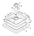
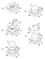
本発明の実施形態について図1〜3を用いて説明する。図1は、本実施形態の発光装置の構成を示す断面図である。図2は、本実施形態の発光装置の要部構成を示す上面図である。図3は、本実施形態の発光装置の構成を示す分解斜視図である。図4は、本実施形態の発光装置の製造方法を説明する斜視図である。 An embodiment of the present invention will be described with reference to FIGS. FIG. 1 is a cross-sectional view showing the configuration of the light emitting device of this embodiment. FIG. 2 is a top view illustrating a configuration of a main part of the light emitting device according to the present embodiment. FIG. 3 is an exploded perspective view showing the configuration of the light emitting device of this embodiment. FIG. 4 is a perspective view illustrating a method for manufacturing the light emitting device of this embodiment.
先ず、本実施形態の基本的な構成について説明する。本実施形態の発光装置は、図1に示すように、LEDチップ1と、実装基板2と、封止部3と、レンズ4と、色変換部材5とを備えている。 First, the basic configuration of this embodiment will be described. As shown in FIG. 1, the light emitting device of the present embodiment includes an
LEDチップ1は、青色光を放射するGaN系青色LEDチップであり、導電性基板10と、発光部11とを備えている。導電性基板10は、結晶成長用基板としてサファイア基板に比べて格子定数や結晶構造がGaNに近くかつ導電性を有するn形のSiC基板からなるものである。上記導電性基板10は、後述する発光部11の上面110と対向する下面100においてサブマウント部材12と接合することにより、後述する金属板20に実装されている。一方、発光部11は、導電性基板10の上面101側にGaN系化合物半導体材料によって形成されて、例えばダブルヘテロ構造を有する積層構造部からなり、エピタキシャル成長法(例えば、MOVPE法など)により成長されたものである。上記発光部11は、上面110及び上面110に延設される複数の側面111,111から青色光を放射する。また、導電性基板10の下面100には、カソード側の電極であるカソード電極(n電極)(図示せず)が形成されているとともに、発光部11の上面110には、アノード側の電極であるアノード電極(p電極)(図示せず)が形成されている。上記カソード電極及び上記アノード電極はNi膜とAu膜との積層膜によって構成されているが、上記カソード電極及び上記アノード電極の材料は特に限定されるものではなく、良好なオーミック特性が得られる材料であればよく、例えばAlなどであってもよい。 The
サブマウント部材12は、LEDチップ1のチップサイズよりも大きなサイズの矩形板状に形成されているものであり、LEDチップ1と金属板20との線膨張率の差に起因してLEDチップ1に働く応力を緩和する。また、サブマウント部材12は、LEDチップ1で発生した熱を金属板20においてLEDチップ1のチップサイズよりも広い範囲に伝熱させる熱伝導機能を有している。本実施形態では、サブマウント部材12の材料として熱伝導率が比較的高くかつ絶縁性を有するAlNを採用しているが、サブマウント部材12の材料はAlNに限らず、線膨張率が導電性基板10の材料である6H−SiCに比較的近く、かつ熱伝導率が比較的高い材料であればよく、例えば、複合SiC、Siなどを採用してもよい。また、サブマウント部材12は、電極パターンの周囲に、LEDチップ1から放射された光を反射する反射膜(例えば、Ni膜とAg膜との積層膜)(図示せず)を備えている。 The
LEDチップ1では、図2に示すように、カソード電極(図示せず)がサブマウント部材12の表面120に設けられ上記カソード電極と接続する電極パターン(図示せず)、及び金属細線(例えば金細線やアルミニウム細線など)などのボンディングワイヤ13を介して一方のリードパターン23(図2の下側)と電気的に接続し、アノード電極(図示せず)がボンディングワイヤ13を介して他方のリードパターン23(図2の上側)と電気的に接続している。なお、LEDチップ1とサブマウント部材12は、例えば、SnPb、AuSn、SnAgCuなどの半田や、銀ペーストなどを用いて接合すればよいが、AuSn、SnAgCuなどの鉛フリー半田を用いて接合することが好ましい。 In the
また、図1に示すように、LEDチップ1をサブマウント部材12に接合することにより、LEDチップ1は、後述する実装基板2の絶縁性基材21におけるレンズ4と対向する面である表面210に対してレンズ4側(図1の上側)に突出するように配置されている。 Further, as shown in FIG. 1, by bonding the
実装基板2は、金属板20と、絶縁性基材21とを積層して備えている。金属板20と絶縁性基材21とは、絶縁性を有するシート状の接着フィルムからなる固着材22により固着されている。上記金属板20の材料としてはCuを採用しているが、熱伝導率の比較的高い金属材料であればよく、Cuに限らず、Alなどを採用してもよい。また、金属板20には、LEDチップ1が実装されたサブマウント部材12が実装されている。一方、絶縁性基材21は、例えばガラスエポキシ基板などである。上記絶縁性基材21の表面210には、LEDチップ1の両電極それぞれ(図示せず)と電気的に接続する一対のリードパターン23が設けられている。各リードパターン23は、Ni膜とAu膜との積層膜であり、色変換部材5により覆われていない部位がアウターリード部230,230(図2参照)となっている。また、絶縁性基材21の表面210には、LEDチップ1に対応する部位に窓孔24が設けられ、LEDチップ1で発生した熱が絶縁性基材21を介さずに金属板20に伝熱できるようになっている。 The
封止部3は、弾性を有し、例えばシリコーン樹脂などの透明樹脂を充填(ポッティング)して形成されるものであり、LEDチップ1及びボンディングワイヤ13,13を封止している。本実施形態では、成形金型90,91(図4参照)の内側に透明樹脂を充填して熱硬化させることで封止部3を形成する。なお、封止部3としては、シリコーン樹脂に限定されるものではなく、アクリル樹脂などを用いてもよい。シリコーン樹脂は、エポキシ樹脂やアクリル樹脂よりも耐熱性及び熱伝導率が高いので、高温でも変形することがなく、またLEDチップ1からの熱に対する放熱効果を高めることができる。 The sealing
レンズ4は、例えばシリコーン樹脂などの成形品であり、LEDチップ1側(図1の下側)に凸曲面状に形成される光入射面40と、凸曲面状に形成される光出射面41とを備え、封止部3に重ねて配置されている。つまり、上記レンズ4は両凸レンズである。また、レンズ4は、光軸がLEDチップ1の厚み方向に沿った発光部11の中心線上に位置するように配置されている。上記のように、レンズ4は、光出射面41が凸曲面状に形成されるので、光入射面40から入射した光を光出射面41と上記空気層6との境界で全反射させないようになっている。なお、レンズ4は、封止部3と屈折率が同じ値となっているが、シリコーン樹脂の成形品に限定されるものではなく、例えば、アクリル樹脂の成形品であってもよい。 The
色変換部材5は、透明材料と、蛍光体とを混合した混合物によって、ドーム状に形成された成形品であり、封止部3及びレンズ4を覆い、封止部3及び光出射面41との間に空気層6が形成される形で配置されている。上記色変換部材5は、内面50がレンズ4の光出射面41に沿った形状に形成されている。したがって、レンズ4の光出射面41の位置によらず法線方向における光出射面41と色変換部材5の内面50との間の距離が略一定値となっている。また、色変換部材5は、位置によらず法線方向に沿った肉厚が一様となるように成形されている。さらに、色変換部材5は、例えば接着剤(例えば、シリコーン樹脂、エポキシ樹脂など)を用いて、開口部の周縁を実装基板2の絶縁性基材21に接着されている。透明材料は、例えばシリコーン樹脂などである。なお、上記透明材料は、シリコーン樹脂に限定されるものではなく、例えば、アクリル樹脂、エポキシ樹脂、ガラスなどを採用してもよい。一方、蛍光体は、粒子状であり、LEDチップ1から放射された青色光によって励起されて、LEDチップ1の発光色とは異なる色であるブロードな黄色系の光を放射する。なお、上記蛍光体は、黄色蛍光体に限定されるものではなく、例えば、赤色蛍光体と緑色蛍光体であってもよい。 The
このような色変換部材5は、レンズ4に密着していないので、寸法精度や位置決め精度に起因した歩留まりの低下を抑制する。また、色変換部材5に外力が作用した場合に、色変換部材5に発生した応力がレンズ4及び封止部3を通してLEDチップ1に伝達されることを抑制する。さらに、外部雰囲気中の水分をLEDチップ1に到達しにくい構成になっている。 Since such a
このような本実施形態の発光装置は、例えばグリーンシートなどの絶縁層7を介して金属(例えば、Al、Cuなどの熱伝導率の高い金属)製の器具本体8に実装されることで、LEDチップ1から器具本体8までの熱抵抗を小さくすることができて放熱性が向上し、LEDチップ1のジャンクション温度の温度上昇を抑制することできるので、入力電力を大きくすることができ、光出力の高出力化を図ることができる。 Such a light emitting device of the present embodiment is mounted on an
次に、本実施形態の発光装置の製造方法について図3,4を用いて説明する。図3には、製造前の各構成部品を示している。また、図4は、図3の範囲Aを示している。先ず、図4(a)に示すように、金属板20と絶縁性基材21とが積層された実装基板2に、サブマウント部材12を介してLEDチップ1を実装してボンディングワイヤ13,13(図2参照)のボンディングを行う(第1工程)。なお、図3,4ではボンディングワイヤ13,13の図示を省略している。第1工程後、図4(b)に示すように、一対の半円筒状の成形金型90,91を両成形金型90,91で円筒状の枠体をなすように、絶縁性基材21の表面210にLEDチップ1及びボンディングワイヤ13,13を囲むようにして取り付ける(第2工程)。第2工程後、液状の透明樹脂(シリコーン樹脂)92を入れた容器93から上記透明樹脂92を成形金型90,91の内側に注入する(第3工程)。そして、図4(c)に示すように、上記透明樹脂92が成形金型90,91の内側に充填された状態でレンズ4を用意し、図4(d)に示すように、上記レンズ4を透明樹脂92上に載置してから、透明樹脂92を熱硬化させて封止部3を形成するとともに封止部3とレンズ4とを固着する(第4工程)。続いて、図4(e)に示すように、成形金型90,91を離型する(第5工程)。最後に、接着剤などを用いて、図3に示す色変換部材5を絶縁性基材21の表面210に固着する(第6工程)。 Next, the manufacturing method of the light-emitting device of this embodiment is demonstrated using FIG. In FIG. 3, each component before manufacture is shown. FIG. 4 shows a range A in FIG. First, as shown in FIG. 4 (a), the
続いて、本実施形態の発光装置においてLEDチップ1から放射された光の光路について図1を用いて説明する。先ず、LEDチップ1の発光部11の上面110から放射された青色光について説明する。上記発光部11の上面110から垂直方向(図1の上方向)に放射された青色光は、封止部3、レンズ4及び空気層6を順に伝搬して色変換部材5に到達し、上記発光部11の上面110から平行方向(図1の左右方向)に放射された青色光は、封止部3及び空気層6を順に伝搬して色変換部材5に到達する。続いて、色変換部材5に到達した青色光によって、蛍光体が励起されて黄色光を放射する。最後に、LEDチップ1から放射された青色光と、色変換部材5の蛍光体から放射された黄色光との組み合わせによって、白色光が色変換部材5の外面51から放射される。 Next, the optical path of the light emitted from the
一方、LEDチップ1の発光部11の側面111,111から放射された青色光について説明する。上記発光部11の側面111,111から垂直方向(図1の左右方向)に放射された青色光は、封止部3及び空気層6を順に伝搬して色変換部材5に到達し、上記発光部11の側面111,111から平行方向(図1の上方向)に放射された青色光は、封止部3、レンズ4及び空気層6を順に伝搬して色変換部材5に到達する。続いて、発光部11の上面110から放射された場合と同様に、色変換部材5に到達した青色光によって、蛍光体が励起されて黄色光を放射し、上記青色光と黄色光との組み合わせによって、白色光が色変換部材5の外面51から放射される。 On the other hand, the blue light radiated | emitted from the side surfaces 111 and 111 of the
上記より、LEDチップ1の発光部11から図1の上方向に放射された青色光だけでなく、LEDチップ1の発光部11から図1の左右方向に放射された青色光も実装基板2に遮断されることなく、色変換部材5に到達することができ、白色光を外部に放射することができる。なお、色変換部材5の蛍光体が赤色蛍光体と緑色蛍光体の場合であっても、同様に白色光を放射することができる。 From the above, not only the blue light emitted from the
次に、本実施形態の発光装置においてLEDチップ1からの熱の流れについて説明する。先ず、LEDチップ1からの熱の一部は、サブマウント部材12を介して金属板20に伝導する。続いて、高い熱伝導性を有する金属板20が放熱を行う。一方、LEDチップ1からの熱の残部は、封止部3に伝導し、封止部3によって放熱が行われる。 Next, the flow of heat from the
上記より、LEDチップ1及び発光装置全体の温度が異常に高くなることを防止することができる。 From the above, it is possible to prevent the temperatures of the
以上、本実施形態によれば、LEDチップ1の発光部11の上面110から平行方向(図1の左右方向)に放射された光や側面111,111から垂直方向(図1の左右方向)に放射された光が実装基板2で遮断することなく封止部3を透過して外部を照射することができるので、LEDチップ1から放射された光を効率よく取り出すことができる。 As described above, according to the present embodiment, the light emitted from the
LEDチップ1から放射された光が凸曲面状の光入射面40からレンズ4に入射するので、指向性を向上させることができる。また、LEDチップ1から放射された青色光と、色変換部材5の蛍光体から放射された黄色光との混色光である白色光の取り出し効率を高めることができるので、光出力の向上をさらに図ることができる。 Since light emitted from the
色変換部材5がレンズ4に密着していないので、色変換部材5の寸法精度や位置決め精度に起因した歩留まりの低下を抑制することができるとともに、色変換部材5に外力が作用した場合に、色変換部材5に発生した応力がレンズ4及び封止部3を通してLEDチップ1に伝達されることを抑制することができる。また、外部雰囲気中の水分をLEDチップ1に到達しにくくすることができる。 Since the
なお、本実施形態の変形例として、LEDチップを、発光部が導電性基板よりも金属板に近い側となるように、金属板に実装してもよい。このような構成にしても、導電性基板と発光部が同程度の屈折率を有している場合、光の取り出し損失が大きくなりすぎることがなく、本実施形態と同様の動作を行うことができる。 As a modification of the present embodiment, the LED chip may be mounted on the metal plate such that the light emitting unit is closer to the metal plate than the conductive substrate. Even in such a configuration, when the conductive substrate and the light emitting unit have the same refractive index, the light extraction loss does not become too large, and the same operation as in the present embodiment can be performed. it can.
1 LEDチップ
11 発光部
110 上面
111 側面
2 実装基板
21 絶縁性基材
210 表面
3 封止部
4 レンズ
5 色変換部材
6 空気層DESCRIPTION OF
Claims (1)
Translated fromJapanese前記LEDチップの前記一の面と対向する他の面で前記LEDチップが実装される実装基板と、
透明樹脂を充填して形成されて前記LEDチップ及び前記LEDチップに接続されるボンディングワイヤを封止するとともに弾性を有する封止部と、
前記LEDチップ側に光入射面及び光出射面が凸曲面状に形成され前記封止部に重ねて配置されるレンズと、
前記LEDチップから放射された光によって励起されて前記LEDチップの発光色とは異なる色の光を放射する蛍光体を含むとともに前記レンズ及び前記封止部を覆い前記レンズの前記光出射面及び前記封止部との間に空気層が形成される形で配置されるドーム状の色変換部材と
を備え、
前記LEDチップが、前記実装基板の前記レンズと対向する面に対して前記レンズ側に突出する
ことを特徴とする発光装置。An LED chip that emits light from one surface and a side surface extending to the one surface;
A mounting substrate on which the LED chip is mounted on the other surface facing the one surface of the LED chip;
A sealing part which is formed by filling a transparent resin and seals the LED chip and the bonding wire connected to the LED chip and has elasticity;
A lens on which the light incident surface and the light output surface are formed in a convex curved surface on the LED chip side and are arranged to overlap the sealing portion;
The phosphor includes a phosphor that is excited by light emitted from the LED chip and emits light of a color different from the emission color of the LED chip, covers the lens and the sealing portion, and the light emitting surface of the lens A dome-shaped color conversion member disposed in a form in which an air layer is formed between the sealing portion and
The LED chip protrudes toward the lens with respect to a surface of the mounting substrate facing the lens.
Priority Applications (1)
| Application Number | Priority Date | Filing Date | Title |
|---|---|---|---|
| JP2005272842AJP4742772B2 (en) | 2005-09-20 | 2005-09-20 | Light emitting device |
Applications Claiming Priority (1)
| Application Number | Priority Date | Filing Date | Title |
|---|---|---|---|
| JP2005272842AJP4742772B2 (en) | 2005-09-20 | 2005-09-20 | Light emitting device |
Publications (2)
| Publication Number | Publication Date |
|---|---|
| JP2007088076Atrue JP2007088076A (en) | 2007-04-05 |
| JP4742772B2 JP4742772B2 (en) | 2011-08-10 |
Family
ID=37974787
Family Applications (1)
| Application Number | Title | Priority Date | Filing Date |
|---|---|---|---|
| JP2005272842AExpired - LifetimeJP4742772B2 (en) | 2005-09-20 | 2005-09-20 | Light emitting device |
Country Status (1)
| Country | Link |
|---|---|
| JP (1) | JP4742772B2 (en) |
Cited By (1)
| Publication number | Priority date | Publication date | Assignee | Title |
|---|---|---|---|---|
| JP2010129598A (en)* | 2008-11-25 | 2010-06-10 | Toshiba Corp | Light emitting apparatus and method for manufacturing the same |
Citations (7)
| Publication number | Priority date | Publication date | Assignee | Title |
|---|---|---|---|---|
| JP2000058925A (en)* | 1998-08-12 | 2000-02-25 | Stanley Electric Co Ltd | LED lamp |
| JP2000208818A (en)* | 1999-01-13 | 2000-07-28 | Asahi Rubber:Kk | Light emitting device |
| JP2002299699A (en)* | 2001-03-30 | 2002-10-11 | Sumitomo Electric Ind Ltd | Light emitting device and method of manufacturing the same |
| JP2003110146A (en)* | 2001-07-26 | 2003-04-11 | Matsushita Electric Works Ltd | Light emitting device |
| JP2003234008A (en)* | 2002-02-06 | 2003-08-22 | Nichia Chem Ind Ltd | Surface emitting device |
| JP2004276383A (en)* | 2003-03-14 | 2004-10-07 | Asahi Rubber:Kk | Method for manufacturing resin lens for semiconductor optical element |
| JP2005158949A (en)* | 2003-11-25 | 2005-06-16 | Matsushita Electric Works Ltd | Light emitting device |
- 2005
- 2005-09-20JPJP2005272842Apatent/JP4742772B2/ennot_activeExpired - Lifetime
Patent Citations (7)
| Publication number | Priority date | Publication date | Assignee | Title |
|---|---|---|---|---|
| JP2000058925A (en)* | 1998-08-12 | 2000-02-25 | Stanley Electric Co Ltd | LED lamp |
| JP2000208818A (en)* | 1999-01-13 | 2000-07-28 | Asahi Rubber:Kk | Light emitting device |
| JP2002299699A (en)* | 2001-03-30 | 2002-10-11 | Sumitomo Electric Ind Ltd | Light emitting device and method of manufacturing the same |
| JP2003110146A (en)* | 2001-07-26 | 2003-04-11 | Matsushita Electric Works Ltd | Light emitting device |
| JP2003234008A (en)* | 2002-02-06 | 2003-08-22 | Nichia Chem Ind Ltd | Surface emitting device |
| JP2004276383A (en)* | 2003-03-14 | 2004-10-07 | Asahi Rubber:Kk | Method for manufacturing resin lens for semiconductor optical element |
| JP2005158949A (en)* | 2003-11-25 | 2005-06-16 | Matsushita Electric Works Ltd | Light emitting device |
Cited By (2)
| Publication number | Priority date | Publication date | Assignee | Title |
|---|---|---|---|---|
| JP2010129598A (en)* | 2008-11-25 | 2010-06-10 | Toshiba Corp | Light emitting apparatus and method for manufacturing the same |
| US8198647B2 (en) | 2008-11-25 | 2012-06-12 | Kabushiki Kaisha Toshiba | Light emitting apparatus |
Also Published As
| Publication number | Publication date |
|---|---|
| JP4742772B2 (en) | 2011-08-10 |
Similar Documents
| Publication | Publication Date | Title |
|---|---|---|
| JP2007287713A (en) | Light emitting device and manufacturing method thereof | |
| JP2007103926A (en) | Led illumination device | |
| JP4029918B2 (en) | LED lighting device | |
| JP2007088078A (en) | Light-emitting device | |
| JP4925346B2 (en) | Light emitting device | |
| JP4742772B2 (en) | Light emitting device | |
| JP2007116124A (en) | Light emitting device | |
| JP3941826B2 (en) | LED luminaire manufacturing method | |
| JP4820133B2 (en) | Light emitting device | |
| JP4765507B2 (en) | Light emitting device | |
| JP2007274010A (en) | Light emitting device and method of manufacturing same | |
| JP4829577B2 (en) | Light emitting device | |
| JP3952075B2 (en) | Light emitting device | |
| JP4483771B2 (en) | Light emitting device and manufacturing method thereof | |
| JP2007088093A (en) | Light-emitting device | |
| JP4742761B2 (en) | Light emitting device | |
| JP4458008B2 (en) | Light emitting device | |
| JP3963187B2 (en) | Light emitting device | |
| JP4556815B2 (en) | Light emitting device | |
| JP2007116123A (en) | Light emitting device | |
| JP2007088084A (en) | Light-emitting device | |
| JP3963188B2 (en) | Light emitting device | |
| JP4483772B2 (en) | Light emitting device and manufacturing method thereof | |
| JP2007088082A (en) | Light-emitting device | |
| JP2007087668A (en) | Luminaire |
Legal Events
| Date | Code | Title | Description |
|---|---|---|---|
| A621 | Written request for application examination | Free format text:JAPANESE INTERMEDIATE CODE: A621 Effective date:20080610 | |
| A977 | Report on retrieval | Free format text:JAPANESE INTERMEDIATE CODE: A971007 Effective date:20100217 | |
| A131 | Notification of reasons for refusal | Free format text:JAPANESE INTERMEDIATE CODE: A131 Effective date:20100223 | |
| RD04 | Notification of resignation of power of attorney | Free format text:JAPANESE INTERMEDIATE CODE: A7424 Effective date:20100713 | |
| A131 | Notification of reasons for refusal | Free format text:JAPANESE INTERMEDIATE CODE: A131 Effective date:20101012 | |
| A521 | Written amendment | Free format text:JAPANESE INTERMEDIATE CODE: A523 Effective date:20101213 | |
| TRDD | Decision of grant or rejection written | ||
| A01 | Written decision to grant a patent or to grant a registration (utility model) | Free format text:JAPANESE INTERMEDIATE CODE: A01 Effective date:20110412 | |
| A61 | First payment of annual fees (during grant procedure) | Free format text:JAPANESE INTERMEDIATE CODE: A61 Effective date:20110425 | |
| FPAY | Renewal fee payment (event date is renewal date of database) | Free format text:PAYMENT UNTIL: 20140520 Year of fee payment:3 | |
| R151 | Written notification of patent or utility model registration | Ref document number:4742772 Country of ref document:JP Free format text:JAPANESE INTERMEDIATE CODE: R151 | |
| FPAY | Renewal fee payment (event date is renewal date of database) | Free format text:PAYMENT UNTIL: 20140520 Year of fee payment:3 |