JP2007082170A - Dual band antenna - Google Patents
Dual band antennaDownload PDFInfo
- Publication number
- JP2007082170A JP2007082170AJP2006026997AJP2006026997AJP2007082170AJP 2007082170 AJP2007082170 AJP 2007082170AJP 2006026997 AJP2006026997 AJP 2006026997AJP 2006026997 AJP2006026997 AJP 2006026997AJP 2007082170 AJP2007082170 AJP 2007082170A
- Authority
- JP
- Japan
- Prior art keywords
- strip
- ground plane
- band antenna
- antenna according
- dual
- Prior art date
- Legal status (The legal status is an assumption and is not a legal conclusion. Google has not performed a legal analysis and makes no representation as to the accuracy of the status listed.)
- Granted
Links
Images


Classifications
- H—ELECTRICITY
- H01—ELECTRIC ELEMENTS
- H01Q—ANTENNAS, i.e. RADIO AERIALS
- H01Q9/00—Electrically-short antennas having dimensions not more than twice the operating wavelength and consisting of conductive active radiating elements
- H01Q9/04—Resonant antennas
- H01Q9/30—Resonant antennas with feed to end of elongated active element, e.g. unipole
- H01Q9/42—Resonant antennas with feed to end of elongated active element, e.g. unipole with folded element, the folded parts being spaced apart a small fraction of the operating wavelength
- H—ELECTRICITY
- H01—ELECTRIC ELEMENTS
- H01Q—ANTENNAS, i.e. RADIO AERIALS
- H01Q5/00—Arrangements for simultaneous operation of antennas on two or more different wavebands, e.g. dual-band or multi-band arrangements
- H01Q5/10—Resonant antennas
- H—ELECTRICITY
- H01—ELECTRIC ELEMENTS
- H01Q—ANTENNAS, i.e. RADIO AERIALS
- H01Q1/00—Details of, or arrangements associated with, antennas
- H01Q1/12—Supports; Mounting means
- H01Q1/22—Supports; Mounting means by structural association with other equipment or articles
- H01Q1/24—Supports; Mounting means by structural association with other equipment or articles with receiving set
- H—ELECTRICITY
- H01—ELECTRIC ELEMENTS
- H01Q—ANTENNAS, i.e. RADIO AERIALS
- H01Q5/00—Arrangements for simultaneous operation of antennas on two or more different wavebands, e.g. dual-band or multi-band arrangements
- H01Q5/30—Arrangements for providing operation on different wavebands
- H01Q5/378—Combination of fed elements with parasitic elements
- H—ELECTRICITY
- H01—ELECTRIC ELEMENTS
- H01Q—ANTENNAS, i.e. RADIO AERIALS
- H01Q9/00—Electrically-short antennas having dimensions not more than twice the operating wavelength and consisting of conductive active radiating elements
- H01Q9/04—Resonant antennas
Landscapes
- Waveguide Aerials (AREA)
- Variable-Direction Aerials And Aerial Arrays (AREA)
- Details Of Aerials (AREA)
Abstract
Translated fromJapaneseDescription
Translated fromJapanese本発明は二重帯域アンテナに関し、特に、携帯用端末機に内蔵される二重帯域アンテナに関する。 The present invention relates to a dual band antenna, and more particularly to a dual band antenna built in a portable terminal.
携帯用端末機とは、携帯電話機やPDAなどのように、外部との間での無線によるデータ送受信機能を持ち、かつ持ち運び可能な装置をいう。携帯用端末機に搭載されるアンテナには外部アンテナと内蔵アンテナとがある。外部アンテナは、携帯用端末機の筐体の外側に設置されたアンテナであり、モノポールアンテナやヘリカルアンテナなどを含む。モノポールアンテナは導体の棒を含み、その棒の長さで送受信可能な周波数帯域が決定される。ヘリカルアンテナは、導体板とコイルとの組み合わせを有する。ヘリカルアンテナは一般に、モノポールアンテナより短く構成できる。外部アンテナは一般に携帯用端末機の外側に突き出ているので、携帯用端末機の更なる小型化が阻まれやすく、筐体のデザインの自由度が制限されやすい。また、外部アンテナは外部からの衝撃によって損傷を受けやすい。従って、近年の携帯用端末機(特に携帯電話機)では、内蔵アンテナの搭載が主流になりつつある。 A portable terminal means a portable device such as a mobile phone or a PDA that has a wireless data transmission / reception function with the outside. There are two types of antennas mounted on portable terminals: an external antenna and a built-in antenna. The external antenna is an antenna installed outside the casing of the portable terminal, and includes a monopole antenna and a helical antenna. The monopole antenna includes a conductor rod, and the frequency band in which transmission and reception can be performed is determined by the length of the rod. The helical antenna has a combination of a conductor plate and a coil. Helical antennas can generally be configured shorter than monopole antennas. Since the external antenna generally protrudes outside the portable terminal, further miniaturization of the portable terminal is likely to be hindered, and the degree of freedom in designing the housing is likely to be limited. In addition, the external antenna is easily damaged by an external impact. Accordingly, in recent portable terminals (particularly mobile phones), mounting of built-in antennas is becoming mainstream.
従来の内蔵アンテナとしては、例えば逆Fアンテナ(Inverted F Antenna:IFA)が知られている。図1及び図2に示されているように、逆Fアンテナは一般に立体(3次元)形状であり、接地部10、放射部12、連結部14、給電部16を有する。放射部12は接地部10の上側に配置される。連結部14は放射部12の端に位置し、接地部10と放射部12との間を接続する。給電部16は外部(例えば送信回路)から接地部10を通して供給される電流を放射部12に伝達する。逆Fアンテナでは一般に、インピーダンスマッチングが、給電部16と連結部14との間の距離やそれぞれの位置/サイズの調節で実現される。送受信周波数が2.4GHzに設定される場合、逆Fアンテナのサイズは15mm×15mm×6mm程度である。このように逆Fアンテナは外部アンテナに比べて小型であるので携帯用端末機の更なる小型化を阻まない。更に、逆Fアンテナは携帯用端末機に容易に内蔵されるので、筐体のデザインの自由度を制限しないだけでなく、外部からの衝撃に強い。その他に、逆Fアンテナは外部アンテナに比べて生産が容易である。
携帯用端末機に対しては更なる小型/軽量化が要求されている。それに伴い、内蔵アンテナの更なる小型化が望まれている。しかし、従来の内蔵アンテナでは更なる小型化が困難である。例えば上記の逆Fアンテナでは、放射部と接地部との間隔やそれぞれのサイズでインピーダンスマッチングが決まるので、更なる小型/軽量化が阻まれる。その他に、接地部と給電部との構造の製造工程を更に簡素化することが困難である。 There is a demand for further miniaturization / lightening of portable terminals. Accordingly, further downsizing of the built-in antenna is desired. However, it is difficult to further reduce the size of the conventional built-in antenna. For example, in the above-described inverted-F antenna, impedance matching is determined by the distance between the radiating portion and the grounding portion and the size of each, so that further miniaturization / weight reduction is prevented. In addition, it is difficult to further simplify the manufacturing process of the structure of the grounding portion and the power feeding portion.
携帯用端末機に対しては更に、多重帯域(マルチバンド)での無線通信(例えば、無線LAN(IEEE802.11a/b/g))への対応が望まれている。それに伴い、携帯用端末機に搭載可能な多重帯域アンテナの更なる小型化が望まれている。特に、IEEE802.11a/b/gの二種類の標準動作周波数2.4GHzと5GHzとの両方で動作可能な二重帯域アンテナに対し、更なる小型/軽量化が望まれている。しかし、従来の逆Fアンテナではその実現が困難である。 For portable terminals, it is further desired to support wireless communication in multiple bands (for example, wireless LAN (IEEE802.11a / b / g)). Accordingly, further downsizing of a multiband antenna that can be mounted on a portable terminal is desired. In particular, a further reduction in size / weight is desired for dual-band antennas that can operate at two standard operating frequencies of 2.4 GHz and 5 GHz of IEEE 802.11a / b / g. However, it is difficult to realize the conventional inverted F antenna.
本発明の目的は、携帯用端末機に内蔵可能であり、且つ更なる小型化が可能な二重帯域アンテナ、の提供にある。 An object of the present invention is to provide a dual band antenna that can be built in a portable terminal and can be further miniaturized.
本発明による二重帯域アンテナは、
接地面、
外部から所定の電流の供給を受ける給電部、
一端が接地面と接続され、他端が給電部に接続されている誘導放射部、及び、
一端が接地面と接続され、他端が開放されている寄生放射部、
を有する。好ましくは、誘導放射部と寄生放射部とが、二つの周波数帯域で共振する。更に好ましくは、上記の二つの周波数帯域のうち、高周波帯域では誘導放射部が共振し、低周波帯域では誘導放射部と寄生放射部とが結合して共振する。好ましくは、その高周波帯域が5GHzを含み、その低周波帯域が2.4GHzを含む。The dual band antenna according to the present invention comprises:
contact area,
A power feeding unit that receives a predetermined current from the outside,
One end of which is connected to the ground plane, the other end is connected to the power feeding section, and the induced radiation section, and
A parasitic radiation part with one end connected to the ground plane and the other end open;
Have Preferably, the induced radiation part and the parasitic radiation part resonate in two frequency bands. More preferably, of the two frequency bands described above, the induced radiation part resonates in the high frequency band, and the induced radiation part and the parasitic radiation part resonate in the low frequency band. Preferably, the high frequency band includes 5 GHz and the low frequency band includes 2.4 GHz.
本発明による上記の二重帯域アンテナでは好ましくは、誘導放射部が、少なくとも1回折れ曲がっているストリップであり、又は、寄生放射部が、少なくとも1回折れ曲がっているストリップである。更に好ましくは、誘導放射部と寄生放射部とが接地面と同一平面上に形成されている。 In the above dual-band antenna according to the present invention, preferably, the induction radiating portion is a strip that is bent at least one time, or the parasitic radiating portion is a strip that is bent at least one time. More preferably, the induced radiation part and the parasitic radiation part are formed on the same plane as the ground plane.
その場合、好ましくは、誘導放射部が、
一端が接地面の一辺に対して垂直に接続されている第1ストリップ、
一端が第1ストリップの他端に接続され、接地面の一辺に対して平行に配置されている第2ストリップ、
一端が第2ストリップの他端に接続され、接地面の一辺に対して垂直に配置されている第3ストリップ、及び、
一端が第3ストリップの他端に接続され、他端が給電部に接続され、接地面の一辺に対して平行に配置されている第4ストリップ、
を有する。更に好ましくは、第1ストリップ、第2ストリップ、第3ストリップ、及び第4ストリップが一体形成されている。In that case, preferably, the induced radiation portion is
A first strip having one end connected perpendicular to one side of the ground plane;
A second strip having one end connected to the other end of the first strip and disposed parallel to one side of the ground plane;
A third strip having one end connected to the other end of the second strip and disposed perpendicular to one side of the ground plane; and
A fourth strip having one end connected to the other end of the third strip, the other end connected to the power feeding portion, and arranged parallel to one side of the ground plane;
Have More preferably, the first strip, the second strip, the third strip, and the fourth strip are integrally formed.
誘導放射部と寄生放射部とが接地面と同一平面上に形成されている場合、好ましくは、寄生放射部が、
一端が接地面の一辺に対して垂直に接続されている第5ストリップ、
一端が第5ストリップの他端に接続され、接地面の一辺に対して平行に配置されている第6ストリップ、
一端が第6ストリップの他端に接続され、接地面の一辺に対して垂直に配置されている第7ストリップ、及び、
一端が第7ストリップの他端に接続され、他端が開放され、接地面の一辺に対して平行に配置されている第8ストリップ、
を有する。更に好ましくは、第5ストリップ、第6ストリップ、第7ストリップ、及び第8ストリップが一体形成されている。When the induced radiation part and the parasitic radiation part are formed on the same plane as the ground plane, preferably, the parasitic radiation part is
A fifth strip having one end connected perpendicular to one side of the ground plane;
A sixth strip having one end connected to the other end of the fifth strip and arranged parallel to one side of the ground plane;
A seventh strip having one end connected to the other end of the sixth strip and disposed perpendicular to one side of the ground plane; and
An eighth strip having one end connected to the other end of the seventh strip and the other end open and arranged parallel to one side of the ground plane;
Have More preferably, the fifth strip, the sixth strip, the seventh strip, and the eighth strip are integrally formed.
その他に、寄生放射部が、
一端が接地面の一辺に対して垂直に接続されている第9ストリップ、及び、
一端が第9ストリップの他端に接続され、他端が開放され、接地面の一辺に対して平行に配置されている第10ストリップ、
を有しても良い。その場合、好ましくは、第9ストリップと第10ストリップとが一体形成されている。更に好ましくは、第10ストリップと接地面の一辺との間の距離が第2ストリップと接地面の一辺との間の距離より所定量だけ大きい。In addition, the parasitic radiation part
A ninth strip having one end connected perpendicular to one side of the ground plane; and
A tenth strip having one end connected to the other end of the ninth strip and the other end open and arranged parallel to one side of the ground plane;
You may have. In that case, preferably, the ninth strip and the tenth strip are integrally formed. More preferably, the distance between the tenth strip and one side of the ground plane is a predetermined amount greater than the distance between the second strip and one side of the ground plane.
好ましくは、
上記の給電部が、外部のプリント回路基板(PCB)の信号入力端から直接、上記の誘導放射部に電流を供給するように構成されている。Preferably,
The power feeding unit is configured to supply current to the induction radiating unit directly from a signal input terminal of an external printed circuit board (PCB).
本発明による上記の二重帯域アンテナは、誘導放射部と寄生放射部とを二つの周波数帯域で共振させることにより、二重帯域での使用が可能である。更に、誘導放射部と寄生放射部とが接地面と同一平面に配置され得るので、構造の2次元化が容易である。従って、本発明による上記の二重帯域アンテナは、従来の逆Fアンテナを用いた3次元構造の二重帯域アンテナとは異なり、更なる小型化が容易である。その上、外部のPCBの信号入力端から誘導放射部に直接、電流が供給されるように給電部が構成され得るので、製造工程の更なる簡単化が容易である。 The dual band antenna according to the present invention can be used in a double band by resonating the induction radiating part and the parasitic radiating part in two frequency bands. Furthermore, since the induced radiation part and the parasitic radiation part can be arranged on the same plane as the ground plane, the structure can be easily two-dimensionalized. Therefore, the above-described dual-band antenna according to the present invention can be easily reduced in size, unlike a three-dimensional dual-band antenna using a conventional inverted-F antenna. In addition, since the power feeding unit can be configured so that a current is directly supplied from the signal input terminal of the external PCB to the induction radiating unit, the manufacturing process can be further simplified.
以下、添付した図面に基づいて本発明の実施形態による二重帯域アンテナについて詳細に説明する。
≪第1実施形態≫
本発明の第1実施形態による二重帯域アンテナは、誘導放射部110、寄生放射部120、給電部130、及び接地面140を有する(図3参照)。これらは好ましくは、同じ基板上に形成されている。すなわち、本発明の第1実施形態による二重帯域アンテナは平面(2次元)構造を有する。Hereinafter, a dual band antenna according to an embodiment of the present invention will be described in detail with reference to the accompanying drawings.
<< First Embodiment >>
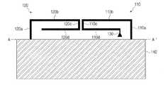
The dual-band antenna according to the first embodiment of the present invention includes an
誘導放射部110は、図3に示されているようなループ状のモノポールアンテナ構造を有し、一端が接地面140と接続され、他端が給電部130に接続されている。誘導放射部110は所定の高周波帯域で共振する。その高周波帯域は誘導放射部110の全長(共振波長の1/2に相当する)で調節され、好ましくは5GHzを含む。好ましくは、誘導放射部110が、少なくとも1回折れ曲がっているストリップである。図3に示されている例では、誘導放射部110が、第1ストリップ110a、第2ストリップ110b、第3ストリップ110c、及び第4ストリップ110dを含む。好ましくは、第1ストリップ110a、第2ストリップ110b、第3ストリップ110c、及び第4ストリップ110dが一つのストリップとして一体形成されている。第1ストリップ110aは、一端が接地面140の一辺AA’に対して垂直に接続され、他端が第2ストリップ110bの一端に接続されている。第2ストリップ110bは、一端が第1ストリップ110aの他端に接続され、他端が第3ストリップ110cの一端に接続され、接地面140の一辺AA’に対して平行に配置されている。第3ストリップ110cは、一端が第2ストリップ110bの他端に接続され、他端が第4ストリップ110dの一端に接続され、接地面140の一辺AA’に対して垂直に配置されている。第4ストリップ110dは、一端が第3ストリップ110cの他端に接続され、他端が給電部130に接続され、接地面140の一辺AA’に対して平行に配置されている。第1〜第4ストリップ110a、110b、110c、110dは接地面140と同一平面上に配置されている。以上の2次元構造により、誘導放射部110の占める面積は小さい。 The induced radiating
寄生放射部120は、誘導放射部110と相似なループ状の構造を有し、一端が接地面140と接続され、他端が開放されている。その構造により、寄生放射部120は誘導放射部110と電磁気的に結合して共振する。ここで、寄生放射部120と誘導放射部110との間の結合により、アンテナの実質的な長さが誘導放射部110と寄生放射部120とのそれぞれの長さより増大する。その結果、共振周波数帯域が、誘導放射部110単独での共振周波数帯域(好ましくは、5GHz近傍)より低い。その低周波帯域は寄生放射部120の長さで調節され、好ましくは2.4GHzを含む。好ましくは、寄生放射部120が、少なくとも1回折れ曲がっているストリップである。図3に示されている例では、寄生放射部120が、第5ストリップ120a、第6ストリップ120b、第7ストリップ120c、及び第8ストリップ120dを含む。好ましくは、第5ストリップ120a、第6ストリップ120b、第7ストリップ120c、及び第8ストリップ120dが一つのストリップとして一体形成されている。第5ストリップ120aは、一端が接地面140の一辺AA’に対して垂直に接続され、他端が第6ストリップ120bの一端に接続されている。第6ストリップ120bは、一端が第5ストリップ120aの他端に接続され、他端が第7ストリップ120cの一端に接続され、接地面140の一辺AA’に対して平行に配置されている。第7ストリップ120cは、一端が第6ストリップ120bの他端に接続され、他端が第8ストリップ120dの一端に接続され、接地面140の一辺AA’に対して垂直に配置されている。第8ストリップ120dは、一端が第7ストリップ120cの他端に接続され、他端が開放され、接地面140の一辺AA’に対して平行に配置されている。第5〜第8ストリップ120a、120b、120c、120dは接地面140と同一平面上に配置されている。以上の2次元構造により、寄生放射部120の占める面積は小さい。このように、誘導放射部110、寄生放射部120、及び接地面140がいずれも同一平面に形成されているので、従来の立体(3次元)構造の逆Fアンテナとは異なり、更なる小型化が容易である。 The
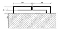
図4は、誘導放射部110と寄生放射部120との各サイズの一例を示す。ここで、誘導放射部110と寄生放射部120とに含まれている各ストリップの厚さは約0.8mmである。図4に示されているサイズでは、誘導放射部110単独の共振による高周波帯域が5.3GHzを中心とし、誘導放射部110と寄生放射部120との間の共振による低周波帯域が2.4GHzを中心とする。図4に示されている例では、本発明の第1実施形態による二重帯域アンテナのサイズが18mm×3mm×0.8mmであり、従来の逆Fアンテナ(例えば図2参照)の典型的なサイズ(動作周波数が2.4GHzである場合、15mm×15mm×6mm)より極めて小さい。このように、本発明の第1実施形態による二重帯域アンテナは、動作周波数帯域が低周波帯域(図4に示されている例では中心値:2.4GHz)と高周波帯域(図4に示されている例では中心値:5.3GHz)との二つに多重化されているにも関わらず、従来の逆Fアンテナより著しく小型化に有利である。 FIG. 4 shows an example of each size of the induced
給電部130は、好ましくは、外部のPCBの信号入力端(図示せず)から直接、誘導放射部110に電流が供給されるように、構成されている。この構造は、従来の逆Fアンテナの給電部の構造より簡単である。図5Aは、給電部130から誘導放射部110に対して電流が上記の高周波帯域に属する周波数で供給される時に生じる表面電流分布を示す。図5Bは、給電部130から誘導放射部110に対して電流が上記の低周波帯域に属する周波数で供給される時に生じる表面電流分布を示す。図5A、5Bとも、表面電流が大きい部分ほど色が濃く描かれている。図5Aに示されているように、給電部130から誘導放射部110に対して供給される電流の周波数が上記の高周波帯域(5GHzを含む)に属する場合、表面電流分布が誘導放射部110に集中している(図5Aに示されている領域RA参照)。従って、高周波帯域では、誘導放射部110が単独で共振していることが分かる。一方、図5Bに示されているように、給電部130から誘導放射部110に対して供給される電流の周波数が上記の低周波帯域(2GHzを含む)に属する場合、表面電流分布が寄生放射部120全体に拡大している(図5Bに示されている領域RB参照)。特に、誘導放射部110と寄生放射部120との間で表面電流分布が大きなループを描いている。従って、低周波帯域では、寄生放射部110が誘導放射部110と結合して共振していることが分かる。 The
図9Aは本発明の第1実施形態による二重帯域アンテナの反射損失の周波数特性を示す。図9Aに示されているように、本発明の第1実施形態による二重帯域アンテナでは、2.4GHzと5GHzとの2カ所の近傍で反射損失が−10dB以下まで急減している。更に、反射損失が−10dBを下回る範囲の幅が比較的広い。従って、本発明の第1実施形態による二重帯域アンテナは実際に、2.4GHz近傍の低周波帯域と5GHz近傍の高周波帯域との二つの周波数帯域で良好に使用可能である。特に、それらの動作周波数帯域がいずれも十分な幅を持つ。 FIG. 9A shows the frequency characteristics of the reflection loss of the dual-band antenna according to the first embodiment of the present invention. As shown in FIG. 9A, in the dual-band antenna according to the first embodiment of the present invention, the reflection loss rapidly decreases to −10 dB or less in the vicinity of two locations of 2.4 GHz and 5 GHz. Furthermore, the width of the range where the reflection loss is less than −10 dB is relatively wide. Therefore, the dual band antenna according to the first embodiment of the present invention can actually be used well in two frequency bands, a low frequency band near 2.4 GHz and a high frequency band near 5 GHz. In particular, all of these operating frequency bands have a sufficient width.
図10Aは本発明の第1実施形態による二重帯域アンテナの放射パターンを示す。図10Aに示されているように、本発明の第1実施形態による二重帯域アンテナは、2.4GHz近傍の低周波帯域と5GHz近傍の高周波帯域とのいずれでも、全方位で均一な放射パターンを示す。 FIG. 10A shows a radiation pattern of the dual-band antenna according to the first embodiment of the present invention. As shown in FIG. 10A, the dual band antenna according to the first embodiment of the present invention has a uniform radiation pattern in all directions in both the low frequency band near 2.4 GHz and the high frequency band near 5 GHz. Show.
≪第2実施形態≫
本発明の第2実施形態による二重帯域アンテナは、誘導放射部210、寄生放射部220、給電部230、及び接地面240を有する(図6参照)。これらは好ましくは、同じ基板上に形成されている。すなわち、本発明の第2実施形態による二重帯域アンテナは平面(2次元)構造を有する。<< Second Embodiment >>
The dual-band antenna according to the second embodiment of the present invention includes an
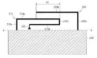
誘導放射部210は、図6に示されているようなループ状のモノポールアンテナ構造を有し、一端が接地面240と接続され、他端が給電部230に接続されている。誘導放射部210は所定の高周波帯域で共振する。その高周波帯域は誘導放射部210の全長(共振波長の1/2に相当する)で調節され、好ましくは5GHzを含む。好ましくは、誘導放射部210が、少なくとも1回折れ曲がっているストリップである。図6に示されている例では、誘導放射部210が、第1ストリップ210a、第2ストリップ210b、第3ストリップ210c、及び第4ストリップ210dを含む。好ましくは、第1ストリップ210a、第2ストリップ210b、第3ストリップ210c、及び第4ストリップ210dが一つのストリップとして一体形成されている。第1ストリップ210aは、一端が接地面240の一辺AA’に対して垂直に接続され、他端が第2ストリップ210bの一端に接続されている。第2ストリップ210bは、一端が第1ストリップ210aの他端に接続され、他端が第3ストリップ210cの一端に接続され、接地面240の一辺AA’に対して平行に配置されている。第3ストリップ210cは、一端が第2ストリップ210bの他端に接続され、他端が第4ストリップ210dの一端に接続され、接地面240の一辺AA’に対して垂直に配置されている。第4ストリップ210dは、一端が第3ストリップ210cの他端に接続され、他端が給電部230に接続され、接地面240の一辺AA’に対して平行に配置されている。第1〜第4ストリップ210a、210b、210c、210dは接地面240と同一平面上に配置されている。以上の2次元構造により、誘導放射部110の占める面積は小さい。 The induced radiating
寄生放射部220は、一端が接地面240と接続され、他端が開放されている。その構造により、寄生放射部220は誘導放射部210と電磁気的に結合して共振する。ここで、寄生放射部220と誘導放射部210との間の結合により、アンテナの実質的な長さが誘導放射部210と寄生放射部220とのそれぞれの長さより増大する。その結果、共振周波数帯域が、誘導放射部210単独での共振周波数帯域(好ましくは、5GHz近傍)より低い。本発明の第2実施形態による二重帯域アンテナでは、特に本発明の第1実施形態による上記の二重帯域アンテナとは異なり、接地面240の一辺AA’に対して垂直な方向で、寄生放射部220の一部が誘導放射部210と重なっている(図6に示されている領域RC参照)。それにより、誘導放射部210と寄生放射部220とが結合して共振するときの共振周波数帯域(低周波帯域)が、寄生放射部220の全長に加え、寄生放射部220と誘導放射部210との間の重なりRCの長さで調節される。好ましくは、その低周波帯域が2.4GHzを含む。好ましくは、寄生放射部220が、少なくとも1回折れ曲がっているストリップである。図6に示されている例では、寄生放射部220が、第9ストリップ220aと第10ストリップ220bとを含む。第9ストリップ220aは、一端が接地面240の一辺AA’に対して垂直に接続され、他端が第10ストリップ220bの一端に接続されている。第10ストリップ220bは、一端が第9ストリップ220aの他端に接続され、他端が開放され、接地面240の一辺AA’に対して平行に配置されている。更に、第10ストリップ220bと接地面240の一辺AA’との間の距離が、第2ストリップ210bと接地面240の一辺AA’との間の距離より所定量だけ大きく設定されている。第9及び第10ストリップ220a、220bは接地面240と同一平面上に配置されている。以上の2次元構造により、寄生放射部120の占める面積は小さい。 The
このように、誘導放射部210、寄生放射部220、及び接地面240がいずれも同一平面に形成されているので、従来の立体(3次元)構造の逆Fアンテナとは異なり、更なる小型化が容易である。本発明の第2実施形態による二重帯域アンテナでは更に、図3の第1実施形態による二重帯域アンテナとは異なり、接地面240の一辺AA’に対して垂直な方向で誘導放射部210と寄生放射部220とを重ねることで、接地面240の一辺AA’に対して平行な方向でのアンテナ全体の長さを低減できる。 As described above, since the
図7は、誘導放射部210と寄生放射部220との各サイズの一例を示す。ここで、誘導放射部210と寄生放射部220とに含まれているストリップの厚さが約0.8mmである。図7に示されているサイズでは、誘導放射部210単独の共振による高周波帯域が5.3GHzを中心とし、誘導放射部210と寄生放射部220との間の共振による低周波帯域が2.4GHzを中心とする。図7に示されている例では、本発明の第2実施形態による二重帯域アンテナのサイズが20mm×5mm×0.8mmであり、従来の逆Fアンテナ(例えば図2参照)の典型的なサイズ(動作周波数が2.4GHzである場合、15mm×15mm×6mm)より極めて小さい。このように、本発明の第2実施形態による二重帯域アンテナは、動作周波数帯域が低周波帯域(図7に示されている例では中心値:2.4GHz)と高周波帯域(図7に示されている例では中心値:5.3GHz)との二つに多重化されているにも関わらず、従来の逆Fアンテナより著しく小型化に有利である。 FIG. 7 shows an example of the sizes of the stimulated
給電部230は、好ましくは、第1実施形態による給電部130(図3参照)と同様に、外部のPCBの信号入力端(図示せず)から直接、誘導放射部210に電流が供給されるように、構成されている。この構造は、従来の逆Fアンテナの給電部の構造より簡単である。図8Aは、給電部230から誘導放射部210に対して電流が上記の高周波帯域に属する周波数で供給される時に生じる表面電流分布を示す。図8Bは、給電部230から誘導放射部210に対して電流が上記の低周波帯域に属する周波数で供給される時に生じる表面電流分布を示す。図5A、5Bとも、表面電流が大きい部分ほど色が濃く描かれている。図8Aに示されているように、給電部230から誘導放射部210に対して供給される電流の周波数が上記の高周波帯域(5GHzを含む)に属する場合、表面電流分布が誘導放射部210に集中している(図8Aに示されている領域RD参照)。従って、高周波帯域では、誘導放射部210が単独で共振していることが分かる。一方、図8Bに示されているように、給電部230から誘導放射部210に対して供給される電流の周波数が上記の低周波帯域(2GHzを含む)に属する場合、表面電流分布が寄生放射部220全体に拡大している(図8Bに示されている領域RE参照)。特に、誘導放射部210と寄生放射部220との間で表面電流分布が大きなループを描いている。従って、低周波帯域では、寄生放射部210が誘導放射部210と結合して共振していることが分かる。 The
図9Bは本発明の第2実施形態による二重帯域アンテナの反射損失の周波数特性を示す。図9Bに示されているように、本発明の第2実施形態による二重帯域アンテナでは、2.4GHzと5GHzとの2カ所の近傍で反射損失が−10dB以下まで急減している。更に、反射損失が−10dBを下回る範囲の幅が比較的広い。従って、本発明の第2実施形態による二重帯域アンテナは実際に、2.4GHz近傍の低周波帯域と5GHz近傍の高周波帯域との二つの周波数帯域で良好に使用可能である。特に、それらの動作周波数帯域がいずれも十分な幅を持つ。 FIG. 9B shows frequency characteristics of reflection loss of the dual-band antenna according to the second embodiment of the present invention. As shown in FIG. 9B, in the dual-band antenna according to the second embodiment of the present invention, the reflection loss rapidly decreases to −10 dB or less in the vicinity of two locations of 2.4 GHz and 5 GHz. Furthermore, the width of the range where the reflection loss is less than −10 dB is relatively wide. Therefore, the dual band antenna according to the second embodiment of the present invention can actually be used well in two frequency bands, a low frequency band near 2.4 GHz and a high frequency band near 5 GHz. In particular, all of these operating frequency bands have a sufficient width.
図10Bは本発明の第2実施形態による二重帯域アンテナの放射パターンを示す。図10Bに示されているように、本発明の第2実施形態による二重帯域アンテナは、2.4GHz近傍の低周波帯域と5GHz近傍の高周波帯域とのいずれでも、全方位で均一な放射パターンを示す。 FIG. 10B shows a radiation pattern of the dual-band antenna according to the second embodiment of the present invention. As shown in FIG. 10B, the dual band antenna according to the second embodiment of the present invention has a uniform radiation pattern in all directions in both the low frequency band near 2.4 GHz and the high frequency band near 5 GHz. Show.
以上、本発明の好適な実施形態について説明した。しかし、本発明は上述の実施形態に限定されるものではない。当業者であれば、特許請求の範囲で請求されている本発明の要旨を逸脱することなく、種々の変更や修正が可能であろう。従って、そのような変更や修正は当然に、本発明の技術的範囲に含まれるべきである。 The preferred embodiments of the present invention have been described above. However, the present invention is not limited to the above-described embodiment. Those skilled in the art will be able to make various changes and modifications without departing from the spirit of the invention as claimed in the claims. Accordingly, such changes and modifications should be included in the technical scope of the present invention.
本発明による二重帯域アンテナは携帯用端末機に内蔵され、上記の構造により更なる小型化を容易にする。このように、本発明は明らかに産業上利用可能である。 The dual band antenna according to the present invention is built in a portable terminal and facilitates further miniaturization by the above structure. Thus, the present invention is clearly industrially applicable.
110 誘導放射部
120 寄生放射部
130 給電部
140 接地面110 Stimulated radiation section
120 Parasitic radiation part
130 Power supply unit
140 Ground plane
Claims (15)
Translated fromJapanese外部から所定の電流の供給を受ける給電部、
一端が前記接地面と接続され、他端が前記給電部に接続されている誘導放射部、及び、
一端が前記接地面と接続され、他端が開放されている寄生放射部、
を有する、二重帯域アンテナ。contact area,
A power feeding unit that receives a predetermined current from the outside,
One end of which is connected to the ground plane and the other end of which is connected to the power feeding section.
A parasitic radiation portion having one end connected to the ground plane and the other end open;
Having a dual band antenna.
一端が前記接地面の一辺に対して垂直に接続されている第1ストリップ、
一端が前記第1ストリップの他端に接続され、前記接地面の一辺に対して平行に配置されている第2ストリップ、
一端が前記第2ストリップの他端に接続され、前記接地面の一辺に対して垂直に配置されている第3ストリップ、及び、
一端が前記第3ストリップの他端に接続され、他端が前記給電部に接続され、前記接地面の一辺に対して平行に配置されている第4ストリップ、
を含む、請求項7に記載の二重帯域アンテナ。The stimulated radiation part is
A first strip having one end connected perpendicular to one side of the ground plane;
A second strip having one end connected to the other end of the first strip and disposed parallel to one side of the ground plane;
A third strip having one end connected to the other end of the second strip and disposed perpendicular to one side of the ground plane; and
A fourth strip having one end connected to the other end of the third strip, the other end connected to the power feeding unit, and arranged parallel to one side of the ground plane;
The dual-band antenna according to claim 7, comprising:
一端が前記接地面の一辺に対して垂直に接続されている第5ストリップ、
一端が前記第5ストリップの他端に接続され、前記接地面の一辺に対して平行に配置されている第6ストリップ、
一端が前記第6ストリップの他端に接続され、前記接地面の一辺に対して垂直に配置されている第7ストリップ、及び、
一端が前記第7ストリップの他端に接続され、他端が開放され、前記接地面の一辺に対して平行に配置されている第8ストリップ、
を含む、請求項7に記載の二重帯域アンテナ。The parasitic radiation part is
A fifth strip having one end connected perpendicular to one side of the ground plane;
A sixth strip having one end connected to the other end of the fifth strip and arranged parallel to one side of the ground plane;
A seventh strip having one end connected to the other end of the sixth strip and arranged perpendicular to one side of the ground plane; and
An eighth strip having one end connected to the other end of the seventh strip, the other end opened, and parallel to one side of the ground plane;
The dual-band antenna according to claim 7, comprising:
一端が前記接地面の一辺に対して垂直に接続されている第9ストリップ、及び、
一端が前記第9ストリップの他端に接続され、他端が開放され、前記接地面の一辺に対して平行に配置されている第10ストリップ、
を含む、請求項7に記載の二重帯域アンテナ。The parasitic radiation part is
A ninth strip having one end connected perpendicular to one side of the ground plane; and
A tenth strip having one end connected to the other end of the ninth strip and the other end open and parallel to one side of the ground plane;
The dual-band antenna according to claim 7, comprising:
Applications Claiming Priority (1)
| Application Number | Priority Date | Filing Date | Title |
|---|---|---|---|
| KR1020050085120AKR100717168B1 (en) | 2005-09-13 | 2005-09-13 | Dual band antenna |
Publications (2)
| Publication Number | Publication Date |
|---|---|
| JP2007082170Atrue JP2007082170A (en) | 2007-03-29 |
| JP4150743B2 JP4150743B2 (en) | 2008-09-17 |
Family
ID=37854520
Family Applications (1)
| Application Number | Title | Priority Date | Filing Date |
|---|---|---|---|
| JP2006026997AExpired - Fee RelatedJP4150743B2 (en) | 2005-09-13 | 2006-02-03 | Dual band antenna |
Country Status (3)
| Country | Link |
|---|---|
| US (1) | US20070057849A1 (en) |
| JP (1) | JP4150743B2 (en) |
| KR (1) | KR100717168B1 (en) |
Cited By (4)
| Publication number | Priority date | Publication date | Assignee | Title |
|---|---|---|---|---|
| WO2008126724A1 (en)* | 2007-04-05 | 2008-10-23 | Murata Manufacturing Co., Ltd. | Antenna and radio communication device |
| WO2014132590A1 (en)* | 2013-02-26 | 2014-09-04 | Necアクセステクニカ株式会社 | Antenna and electronic device |
| WO2015029383A1 (en)* | 2013-08-27 | 2015-03-05 | Necプラットフォームズ株式会社 | Antenna device, and wireless communication device |
| JPWO2022124408A1 (en)* | 2020-12-11 | 2022-06-16 |
Families Citing this family (10)
| Publication number | Priority date | Publication date | Assignee | Title |
|---|---|---|---|---|
| KR100787229B1 (en)* | 2005-02-04 | 2007-12-21 | 삼성전자주식회사 | Dual Band Inverse F Flatten Antenna |
| JP4224081B2 (en)* | 2006-06-12 | 2009-02-12 | 株式会社東芝 | Circularly polarized antenna device |
| US7265720B1 (en)* | 2006-12-29 | 2007-09-04 | Motorola, Inc. | Planar inverted-F antenna with parasitic conductor loop and device using same |
| KR100896486B1 (en)* | 2007-05-16 | 2009-05-08 | 충남대학교산학협력단 | Planar Monopole Antenna for RFID Tag |
| JP5268380B2 (en)* | 2008-01-30 | 2013-08-21 | 株式会社東芝 | ANTENNA DEVICE AND RADIO DEVICE |
| TWI366946B (en)* | 2008-06-26 | 2012-06-21 | Wistron Neweb Corp | Thin antenna and an electronic device having the thin antenna thereof |
| KR101718032B1 (en)* | 2010-11-01 | 2017-03-20 | 엘지전자 주식회사 | Mobile terminal |
| TW201401656A (en)* | 2012-06-26 | 2014-01-01 | Chi Mei Comm Systems Inc | Antenna assembly |
| US10290940B2 (en)* | 2014-03-19 | 2019-05-14 | Futurewei Technologies, Inc. | Broadband switchable antenna |
| EP4429021A1 (en)* | 2023-03-09 | 2024-09-11 | Nokia Technologies Oy | An antenna arrangement |
Citations (2)
| Publication number | Priority date | Publication date | Assignee | Title |
|---|---|---|---|---|
| WO2004025778A1 (en)* | 2002-09-10 | 2004-03-25 | Fractus, S.A. | Coupled multiband antennas |
| JP2004201278A (en)* | 2002-12-06 | 2004-07-15 | Sharp Corp | Pattern antenna |
Family Cites Families (4)
| Publication number | Priority date | Publication date | Assignee | Title |
|---|---|---|---|---|
| US6456249B1 (en)* | 1999-08-16 | 2002-09-24 | Tyco Electronics Logistics A.G. | Single or dual band parasitic antenna assembly |
| FI112724B (en)* | 2000-05-12 | 2003-12-31 | Nokia Corp | Symmetric antenna structure and method of manufacture thereof and the antenna structure applying expansion cards |
| TWI274439B (en)* | 2004-09-17 | 2007-02-21 | Asustek Comp Inc | Telecommunication device and plane antenna thereof |
| JP3775795B1 (en)* | 2005-01-11 | 2006-05-17 | 株式会社東芝 | Wireless device |
- 2005
- 2005-09-13KRKR1020050085120Apatent/KR100717168B1/ennot_activeExpired - Fee Related
- 2006
- 2006-02-03JPJP2006026997Apatent/JP4150743B2/ennot_activeExpired - Fee Related
- 2006-03-24USUS11/387,924patent/US20070057849A1/ennot_activeAbandoned
Patent Citations (3)
| Publication number | Priority date | Publication date | Assignee | Title |
|---|---|---|---|---|
| WO2004025778A1 (en)* | 2002-09-10 | 2004-03-25 | Fractus, S.A. | Coupled multiband antennas |
| JP2005538623A (en)* | 2002-09-10 | 2005-12-15 | フラクトゥス・ソシエダッド・アノニマ | Combined multiband antenna |
| JP2004201278A (en)* | 2002-12-06 | 2004-07-15 | Sharp Corp | Pattern antenna |
Cited By (10)
| Publication number | Priority date | Publication date | Assignee | Title |
|---|---|---|---|---|
| WO2008126724A1 (en)* | 2007-04-05 | 2008-10-23 | Murata Manufacturing Co., Ltd. | Antenna and radio communication device |
| US8378909B2 (en) | 2007-04-05 | 2013-02-19 | Murata Manufacturing Co., Ltd. | Antenna and wireless communication apparatus |
| WO2014132590A1 (en)* | 2013-02-26 | 2014-09-04 | Necアクセステクニカ株式会社 | Antenna and electronic device |
| JP2014165683A (en)* | 2013-02-26 | 2014-09-08 | Nec Access Technica Ltd | Antenna and electronic device |
| CN105009367A (en)* | 2013-02-26 | 2015-10-28 | Nec平台株式会社 | Antenna and electronic device |
| US9685696B2 (en) | 2013-02-26 | 2017-06-20 | Nec Platforms, Ltd. | Antenna and electronic device |
| WO2015029383A1 (en)* | 2013-08-27 | 2015-03-05 | Necプラットフォームズ株式会社 | Antenna device, and wireless communication device |
| JPWO2022124408A1 (en)* | 2020-12-11 | 2022-06-16 | ||
| WO2022124408A1 (en)* | 2020-12-11 | 2022-06-16 | 株式会社ヨコオ | Antenna device |
| JP7717088B2 (en) | 2020-12-11 | 2025-08-01 | 株式会社ヨコオ | Antenna device |
Also Published As
| Publication number | Publication date |
|---|---|
| KR20070030453A (en) | 2007-03-16 |
| JP4150743B2 (en) | 2008-09-17 |
| US20070057849A1 (en) | 2007-03-15 |
| KR100717168B1 (en) | 2007-05-11 |
Similar Documents
| Publication | Publication Date | Title |
|---|---|---|
| JP4150743B2 (en) | Dual band antenna | |
| JP4283278B2 (en) | Dual-band planar antenna | |
| KR100483043B1 (en) | Multi band built-in antenna | |
| US7345634B2 (en) | Planar inverted “F” antenna and method of tuning same | |
| US7193565B2 (en) | Meanderline coupled quadband antenna for wireless handsets | |
| US6714162B1 (en) | Narrow width dual/tri ISM band PIFA for wireless applications | |
| KR100856310B1 (en) | Mobile-communication terminal | |
| US6573869B2 (en) | Multiband PIFA antenna for portable devices | |
| JP2007502562A (en) | ANTENNA DEVICE, MODULE HAVING THE ANTENNA DEVICE, AND RADIO COMMUNICATION DEVICE | |
| US7969371B2 (en) | Small monopole antenna having loop element included feeder | |
| KR100616545B1 (en) | Multi-band laminated chip antenna using double coupling feeding | |
| JP2006187036A (en) | antenna | |
| US6836246B1 (en) | Design of single and multi-band PIFA | |
| WO2004025781A1 (en) | Loop antenna | |
| JP2004147327A (en) | Multi-band antenna | |
| US8081136B2 (en) | Dual-band antenna | |
| KR100367353B1 (en) | Stacked S-type multi-band internal antenna for mobile phone | |
| KR101025970B1 (en) | Antenna for portable terminal and portable terminal having same | |
| KR100808476B1 (en) | Built-in antenna for mobile communication terminal | |
| Hsu et al. | Seven‐band folded‐loop chip antenna for WWAN/WLAN/WiMAX operation in the mobile phone | |
| JP3094677U (en) | Two-band inverted F antenna | |
| JP2006165608A (en) | Small internal antenna | |
| US8816926B2 (en) | Antenna structure | |
| KR101054615B1 (en) | Multiband Antenna for Portable Terminal and Portable Terminal Having Same | |
| KR20080080066A (en) | Multiband antenna |
Legal Events
| Date | Code | Title | Description |
|---|---|---|---|
| A977 | Report on retrieval | Free format text:JAPANESE INTERMEDIATE CODE: A971007 Effective date:20070919 | |
| A131 | Notification of reasons for refusal | Free format text:JAPANESE INTERMEDIATE CODE: A131 Effective date:20070925 | |
| A521 | Request for written amendment filed | Free format text:JAPANESE INTERMEDIATE CODE: A523 Effective date:20071220 | |
| A131 | Notification of reasons for refusal | Free format text:JAPANESE INTERMEDIATE CODE: A131 Effective date:20080122 | |
| A601 | Written request for extension of time | Free format text:JAPANESE INTERMEDIATE CODE: A601 Effective date:20080422 | |
| A602 | Written permission of extension of time | Free format text:JAPANESE INTERMEDIATE CODE: A602 Effective date:20080425 | |
| A521 | Request for written amendment filed | Free format text:JAPANESE INTERMEDIATE CODE: A523 Effective date:20080516 | |
| TRDD | Decision of grant or rejection written | ||
| A01 | Written decision to grant a patent or to grant a registration (utility model) | Free format text:JAPANESE INTERMEDIATE CODE: A01 Effective date:20080610 | |
| A01 | Written decision to grant a patent or to grant a registration (utility model) | Free format text:JAPANESE INTERMEDIATE CODE: A01 | |
| A61 | First payment of annual fees (during grant procedure) | Free format text:JAPANESE INTERMEDIATE CODE: A61 Effective date:20080630 | |
| FPAY | Renewal fee payment (event date is renewal date of database) | Free format text:PAYMENT UNTIL: 20110704 Year of fee payment:3 | |
| R150 | Certificate of patent or registration of utility model | Free format text:JAPANESE INTERMEDIATE CODE: R150 | |
| FPAY | Renewal fee payment (event date is renewal date of database) | Free format text:PAYMENT UNTIL: 20110704 Year of fee payment:3 | |
| FPAY | Renewal fee payment (event date is renewal date of database) | Free format text:PAYMENT UNTIL: 20120704 Year of fee payment:4 | |
| FPAY | Renewal fee payment (event date is renewal date of database) | Free format text:PAYMENT UNTIL: 20120704 Year of fee payment:4 | |
| FPAY | Renewal fee payment (event date is renewal date of database) | Free format text:PAYMENT UNTIL: 20130704 Year of fee payment:5 | |
| R250 | Receipt of annual fees | Free format text:JAPANESE INTERMEDIATE CODE: R250 | |
| LAPS | Cancellation because of no payment of annual fees |