JP2007067275A - Semiconductor element and semiconductor integrated circuit device using the same - Google Patents
Semiconductor element and semiconductor integrated circuit device using the sameDownload PDFInfo
- Publication number
- JP2007067275A JP2007067275AJP2005253521AJP2005253521AJP2007067275AJP 2007067275 AJP2007067275 AJP 2007067275AJP 2005253521 AJP2005253521 AJP 2005253521AJP 2005253521 AJP2005253521 AJP 2005253521AJP 2007067275 AJP2007067275 AJP 2007067275A
- Authority
- JP
- Japan
- Prior art keywords
- terminal
- circuit
- transistor
- substrate bias
- voltage
- Prior art date
- Legal status (The legal status is an assumption and is not a legal conclusion. Google has not performed a legal analysis and makes no representation as to the accuracy of the status listed.)
- Pending
Links
Images


Landscapes
- Read Only Memory (AREA)
- Semiconductor Integrated Circuits (AREA)
- Metal-Oxide And Bipolar Metal-Oxide Semiconductor Integrated Circuits (AREA)
Abstract
Translated fromJapaneseDescription
Translated fromJapanese本発明は電流源または抵抗として機能する半導体素子およびそれを用いた半導体集積回路装置に関するものである。特に基板制御技術の低リーク化効果を最大限に発揮するためにその電流源もしくは抵抗を、基板制御のためのモニタ回路および制御回路に応用する技術に関するものである。 The present invention relates to a semiconductor element functioning as a current source or a resistor and a semiconductor integrated circuit device using the same. In particular, the present invention relates to a technique for applying the current source or resistance to a monitor circuit and a control circuit for substrate control in order to maximize the effect of reducing the leakage of the substrate control technology.
半導体の低消費電力化には待機時のリーク電流の削減が有効である。このリーク電流の削減手法として有効なのが基板制御技術である(例えば、非特許文献1参照)。この基板制御技術というのは、トランジスタの基板電位を制御し逆方向基板バイアス電圧を印加することでリーク電流を削減する技術である。この基板制御技術では単純に逆方向基板バイアスを大きくすれば良いというわけではなく、最適な基板バイアス値が存在する(例えば、非特許文献2参照。)。この最適な基板バイアス電圧は温度、電圧、半導体の仕上がりに大きく依存し、条件により異なっている。しかし、今まではこの最適な基板バイアスをそれぞれの条件に応じて印加する手法が存在せず効果が低かった。
近年、半導体集積回路装置の微細化が進み、トランジスタにおけるリーク電流の増加が大きな問題となってきた。この問題解決のために様々な低リーク化回路技術が提案されている。その中で、低リーク化効果が望める主なものとして基板制御技術がある。ここで、基板制御技術とは、トランジスタの基板電位を制御し、つまり逆方向の基板バイアスを印加し、その結果、半導体のしきい値を高くしてリーク電流を削減するものである。 In recent years, miniaturization of semiconductor integrated circuit devices has progressed, and an increase in leakage current in transistors has become a major problem. In order to solve this problem, various low leakage circuit technologies have been proposed. Among them, there is a substrate control technology that can be expected to have a low leakage effect. Here, the substrate control technique is to control the substrate potential of a transistor, that is, to apply a substrate bias in the reverse direction, and as a result, increase the threshold value of the semiconductor to reduce the leakage current.
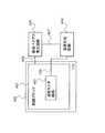
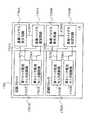
図29(a),(b)に基板制御技術の概要を示す。 29A and 29B show an outline of the substrate control technology.
図29(a)は、半導体集積回路装置として形成したCMOSインバータ回路を例として示している。図29(a)において、符号101はPMOSトランジスタを示す。符号102はNMOSトランジスタを示す。符号103は電圧VBNが与えられるNウエル基板端子を示す。符号104は電圧VDDが与えられる電源端子を示す。符号105はインバータ回路の入力端子を示す。符号106は電圧VSSが与えられるグランド端子を示す。符号107は電圧VBPが与えられるPウエル基板端子を示す。符号108はインバータ回路の出力端子を示す。 FIG. 29A shows a CMOS inverter circuit formed as a semiconductor integrated circuit device as an example. In FIG. 29A,
基板制御技術のCMOSトランジスタは一般的なCMOSトランジスタとは異なり、NMOSトランジスタおよびPMOSトランジスタの基板が電源電位、グランド電位と分離され任意に制御できるようになっていることを特徴とし、基板電圧を制御して逆方向基板バイアスを大きくすることで、リーク電流を減少している。基板制御技術は、その回路の容易性、効果の大きさからリーク電流増加の課題を解決する重要な技術である。 Unlike general CMOS transistors, substrate control technology CMOS transistors are characterized in that the substrate of the NMOS transistor and PMOS transistor is separated from the power supply potential and the ground potential and can be arbitrarily controlled, and the substrate voltage is controlled. By increasing the reverse substrate bias, the leakage current is reduced. Substrate control technology is an important technology that solves the problem of increased leakage current due to the ease and effectiveness of the circuit.
しかし、逆方向基板バイアスは大きければ良いというわけではなく、最適値を持っている。 However, the reverse substrate bias is not necessarily large and has an optimum value.
図29(b)に基板バイアス電圧VBPとリーク電流IDDQとの関係を示す。図29(b)では基板温度が0℃、25℃、50℃の場合の基板バイアス電圧VBPとリーク電流IDDQとの関係を示している。このグラフから分かるように、リーク電流IDDSの特性は温度によって大きく変化し、各温度(0℃、25℃、50℃)でリーク電流を減少するのに最適な基板バイアス電圧が存在する。また、リーク電流の特性は、プロセスの仕上がり、電源電圧にも依存して変化し、リーク電流を最大に削減する基板バイアスの最適値は変化する。一方で、あまり大きな基板バイアスを印加するとデバイスの破壊を招く。 FIG. 29B shows the relationship between the substrate bias voltage VBP and the leakage current IDDQ. FIG. 29B shows the relationship between the substrate bias voltage VBP and the leakage current IDDQ when the substrate temperature is 0 ° C., 25 ° C., and 50 ° C. As can be seen from this graph, the characteristics of the leakage current IDDS vary greatly depending on the temperature, and there is an optimum substrate bias voltage for reducing the leakage current at each temperature (0 ° C., 25 ° C., 50 ° C.). Further, the characteristics of the leakage current change depending on the process finish and the power supply voltage, and the optimum value of the substrate bias for reducing the leakage current to the maximum changes. On the other hand, when a very large substrate bias is applied, the device is destroyed.
以上のように、基板制御技術には状態に応じて低リーク化効果を得る最適な基板バイアス電圧が存在する。従来の技術では状態に応じて基板バイアス電圧を変化させるようなことは行わずに一律の基板バイアス電圧を設定していたため、最大の低リーク化効果を得られず、半導体の低リーク化対策が必ずしも十分でなかった。その理由は基板バイアスを制御するための温度モニタ回路またはリーク電流モニタ回路を容易に実現する素子がなかったためである。 As described above, there is an optimum substrate bias voltage for obtaining a low leakage effect depending on the state in the substrate control technology. In the conventional technology, since the uniform substrate bias voltage is set without changing the substrate bias voltage according to the state, the maximum effect of reducing the leakage cannot be obtained, and measures for reducing the leakage of the semiconductor are taken. Not always enough. The reason is that there is no element that easily realizes a temperature monitor circuit or a leak current monitor circuit for controlling the substrate bias.
したがって、本発明の目的は、基板バイアスを最適に制御してリーク電流を削減することができる半導体集積回路装置を提供することである。 Accordingly, an object of the present invention is to provide a semiconductor integrated circuit device capable of reducing leakage current by optimally controlling a substrate bias.
また、本発明の他の目的は、基板バイアスを制御するために必要なモニタ回路を容易に実現することができる半導体素子を提供することである。 Another object of the present invention is to provide a semiconductor device capable of easily realizing a monitor circuit necessary for controlling the substrate bias.
上記課題を解決するために、本発明の半導体素子は、MOSトランジスタの第1の拡散層端子と第2の拡散層端子とが相互に接続された構造を有し、MOSトランジスタのゲート端子が一端となり、MOSトランジスタの第1の拡散層端子が他端となる。ゲート端子と第1の拡散層端子との間に一定の電圧を印加することにより、ゲート端子と第1の拡散層端子間に一定電流を流すことができ、この半導体素子は、電流源として使用することができる。また、この半導体素子は、抵抗として使用することもできる。 In order to solve the above problems, a semiconductor device of the present invention has a structure in which a first diffusion layer terminal and a second diffusion layer terminal of a MOS transistor are connected to each other, and the gate terminal of the MOS transistor is connected to one end. Thus, the first diffusion layer terminal of the MOS transistor becomes the other end. By applying a constant voltage between the gate terminal and the first diffusion layer terminal, a constant current can flow between the gate terminal and the first diffusion layer terminal. This semiconductor element is used as a current source. can do. The semiconductor element can also be used as a resistor.
上記構成の半導体素子においては、MOSトランジスタの基板端子がMOSトランジスタの第1の拡散層端子および第2の拡散層端子に接続された構造を有する場合もある。 The semiconductor element having the above structure may have a structure in which the substrate terminal of the MOS transistor is connected to the first diffusion layer terminal and the second diffusion layer terminal of the MOS transistor.
上記構成においては、MOSトランジスタが、NMOSトランジスタでも、PMOSトランジスタのどちらでもよい。MOSトランジスタが、NMOSトランジスタである場合には、MOSトランジスタのゲート端子に印加される電圧がMOSトランジスタの第1の拡散層端子に印加される電圧より高く、MOSトランジスタのゲート端子と第1の拡散層端子との間の電圧差が、NMOSトランジスタのしきい値電圧以上であることが好ましい。また、MOSトランジスタが、PMOSトランジスタである場合には、MOSトランジスタのゲート端子に印加される電圧がMOSトランジスタの第1の拡散層端子に印加される電圧より低く、MOSトランジスタのゲート端子と第1の拡散層端子との間の電圧差が、PMOSトランジスタのしきい値電圧以上であることが好ましい。 In the above configuration, the MOS transistor may be either an NMOS transistor or a PMOS transistor. When the MOS transistor is an NMOS transistor, the voltage applied to the gate terminal of the MOS transistor is higher than the voltage applied to the first diffusion layer terminal of the MOS transistor, and the gate terminal and the first diffusion of the MOS transistor The voltage difference with the layer terminal is preferably equal to or higher than the threshold voltage of the NMOS transistor. In the case where the MOS transistor is a PMOS transistor, the voltage applied to the gate terminal of the MOS transistor is lower than the voltage applied to the first diffusion layer terminal of the MOS transistor, It is preferable that the voltage difference with the diffusion layer terminal is equal to or higher than the threshold voltage of the PMOS transistor.
また上記構成の半導体素子においては、MOSトランジスタがマルチゲート構造を有し、MOSトランジスタの全てのゲート端子が共通接続されていてもよい。MOSトランジスタがマルチゲート構造を有する場合、MOSトランジスタが、NMOSトランジスタでも、PMOSトランジスタのどちらでもよい。MOSトランジスタが、NMOSトランジスタである場合には、MOSトランジスタのゲート端子に印加される電圧がMOSトランジスタの第1の拡散層端子に印加される電圧より高く、MOSトランジスタのゲート端子と第1の拡散層端子との間の電圧差が、NMOSトランジスタのしきい値電圧以上であることが好ましい。また、MOSトランジスタが、PMOSトランジスタである場合には、MOSトランジスタのゲート端子に印加される電圧がMOSトランジスタの第1の拡散層端子に印加される電圧より低く、MOSトランジスタのゲート端子と第1の拡散層端子との間の電圧差が、PMOSトランジスタのしきい値電圧以上であることが好ましい。 In the semiconductor element having the above structure, the MOS transistors may have a multi-gate structure, and all the gate terminals of the MOS transistors may be commonly connected. When the MOS transistor has a multi-gate structure, the MOS transistor may be either an NMOS transistor or a PMOS transistor. When the MOS transistor is an NMOS transistor, the voltage applied to the gate terminal of the MOS transistor is higher than the voltage applied to the first diffusion layer terminal of the MOS transistor, and the gate terminal and the first diffusion of the MOS transistor The voltage difference with the layer terminal is preferably equal to or higher than the threshold voltage of the NMOS transistor. In the case where the MOS transistor is a PMOS transistor, the voltage applied to the gate terminal of the MOS transistor is lower than the voltage applied to the first diffusion layer terminal of the MOS transistor, It is preferable that the voltage difference with the diffusion layer terminal is equal to or higher than the threshold voltage of the PMOS transistor.
また、上記構成の半導体素子においては、MOSトランジスタがSOI構造を有していてもよい。MOSトランジスタがSOI構造を有する場合、MOSトランジスタが、NMOSトランジスタでも、PMOSトランジスタのどちらでもよい。MOSトランジスタが、NMOSトランジスタである場合には、MOSトランジスタのゲート端子に印加される電圧がMOSトランジスタの第1の拡散層端子に印加される電圧より高く、MOSトランジスタのゲート端子と第1の拡散層端子との間の電圧差が、NMOSトランジスタのしきい値電圧以上であることが好ましい。また、MOSトランジスタが、PMOSトランジスタである場合には、MOSトランジスタのゲート端子に印加される電圧がMOSトランジスタの第1の拡散層端子に印加される電圧より低く、MOSトランジスタのゲート端子と第1の拡散層端子との間の電圧差が、PMOSトランジスタのしきい値電圧以上であることが好ましい。 In the semiconductor element having the above structure, the MOS transistor may have an SOI structure. When the MOS transistor has an SOI structure, the MOS transistor may be either an NMOS transistor or a PMOS transistor. When the MOS transistor is an NMOS transistor, the voltage applied to the gate terminal of the MOS transistor is higher than the voltage applied to the first diffusion layer terminal of the MOS transistor, and the gate terminal and the first diffusion of the MOS transistor The voltage difference with the layer terminal is preferably equal to or higher than the threshold voltage of the NMOS transistor. In the case where the MOS transistor is a PMOS transistor, the voltage applied to the gate terminal of the MOS transistor is lower than the voltage applied to the first diffusion layer terminal of the MOS transistor, It is preferable that the voltage difference with the diffusion layer terminal is equal to or higher than the threshold voltage of the PMOS transistor.
本発明の半導体集積回路装置は、第1のMOSトランジスタを含み、第1のMOSトランジスタの基板端子が電源端子および接地端子から分離された回路ブロックと、回路ブロック内に設けられた温度モニタ回路と、温度判定回路および基板バイアス発生回路とを備え、温度モニタ回路の出力をもとに温度判定回路で回路ブロックの温度を判定し、温度判定回路の判定出力を基板バイアス発生回路へ入力することにより、回路ブロックの温度に応じた基板バイアスを基板バイアス発生回路から回路ブロックの第1のMOSトランジスタの基板端子へ印加する半導体集積回路装置である。 A semiconductor integrated circuit device of the present invention includes a first MOS transistor, a circuit block in which a substrate terminal of the first MOS transistor is separated from a power supply terminal and a ground terminal, a temperature monitor circuit provided in the circuit block, A temperature determination circuit and a substrate bias generation circuit, the temperature determination circuit determines the temperature of the circuit block based on the output of the temperature monitor circuit, and the determination output of the temperature determination circuit is input to the substrate bias generation circuit The semiconductor integrated circuit device applies a substrate bias corresponding to the temperature of the circuit block from the substrate bias generating circuit to the substrate terminal of the first MOS transistor of the circuit block.
そして、温度モニタ回路は、第1および第2の半導体素子の直列回路からなり、第1の半導体素子は第2のMOSトランジスタのソース端子とゲート端子と基板端子とが相互に接続された構造を有し、第2のMOSトランジスタのドレイン端子が一端となり、第2のMOSトランジスタのソース端子が他端となり、第2の半導体素子は第3のMOSトランジスタのドレイン端子とソース端子と基板端子とが相互に接続された構造を有し、第3のMOSトランジスタのゲート端子が一端となり、第3のMOSトランジスタの第1の拡散層端子が他端となり、第1および第2の半導体素子の直列回路に電圧が印加されることにより、第1および第2の半導体素子の接続点から回路ブロックの温度に応じた信号を出力する。 The temperature monitoring circuit is composed of a series circuit of first and second semiconductor elements, and the first semiconductor element has a structure in which the source terminal, the gate terminal, and the substrate terminal of the second MOS transistor are connected to each other. The drain terminal of the second MOS transistor is one end, the source terminal of the second MOS transistor is the other end, and the second semiconductor element has a drain terminal, a source terminal, and a substrate terminal of the third MOS transistor. A series circuit of first and second semiconductor elements having a mutually connected structure, the gate terminal of the third MOS transistor serving as one end and the first diffusion layer terminal of the third MOS transistor serving as the other end When a voltage is applied to, a signal corresponding to the temperature of the circuit block is output from the connection point of the first and second semiconductor elements.
上記の半導体集積回路装置においては、温度判定回路および基板バイアス発生回路の何れか少なくとも一つは回路ブロックとは分離した状態で形成されていてもよい。 In the semiconductor integrated circuit device, at least one of the temperature determination circuit and the substrate bias generation circuit may be formed in a state separated from the circuit block.
また、上記の半導体集積回路装置においては、回路ブロックを2個以上備え、各回路ブロック内に温度モニタ回路が個別に設けられ、各回路ブロックについて個別に温度判定回路および基板バイアス発生回路が設けられ、各温度モニタ回路の出力をもとに各温度判定回路で各回路ブロックの温度を判定し、各温度判定回路の判定出力を各基板バイアス発生回路へ入力することにより、各回路ブロックの温度に応じた基板バイアスを各基板バイアス発生回路から各回路ブロックのMOSトランジスタの基板端子へ印加してもよい。 The semiconductor integrated circuit device includes two or more circuit blocks, a temperature monitor circuit is individually provided in each circuit block, and a temperature determination circuit and a substrate bias generation circuit are individually provided for each circuit block. The temperature of each circuit block is determined by each temperature determination circuit based on the output of each temperature monitor circuit, and the determination output of each temperature determination circuit is input to each substrate bias generation circuit to obtain the temperature of each circuit block. A corresponding substrate bias may be applied from each substrate bias generating circuit to the substrate terminal of the MOS transistor of each circuit block.
上記構成においては、第2のMOSトランジスタおよび第3のMOSトランジスタが例えば第1および第2のNMOSトランジスタでそれぞれ構成され、第1のNMOSトランジスタはドレイン端子が電源電位に固定され、第2のNMOSトランジスタはドレイン端子が接地電位に固定され、第1のNMOSトランジスタのソース端子と第2のNMOSトランジスタのゲート端子とが接続され、第2のNMOSトランジスタのゲート端子が温度モニタ回路の出力端子となる。 In the above configuration, the second MOS transistor and the third MOS transistor are respectively configured by, for example, first and second NMOS transistors, and the drain terminal of the first NMOS transistor is fixed to the power supply potential, and the second NMOS transistor The drain terminal of the transistor is fixed to the ground potential, the source terminal of the first NMOS transistor and the gate terminal of the second NMOS transistor are connected, and the gate terminal of the second NMOS transistor becomes the output terminal of the temperature monitor circuit. .
また、温度判定回路は例えば1個以上のオペアンプで構成され、温度モニタ回路の出力がオペアンプに入力され、オペアンプの出力が基板バイアス発生回路へ入力され、それぞれのオペアンプのリファレンス電圧にはそれぞれ異なった電位が入力され、それぞれのリファレンス電圧の電位は温度モニタ回路の所定の温度状態における出力に相当する電位である。 The temperature determination circuit is composed of, for example, one or more operational amplifiers, the output of the temperature monitor circuit is input to the operational amplifier, the output of the operational amplifier is input to the substrate bias generation circuit, and the reference voltage of each operational amplifier is different. A potential is input, and the potential of each reference voltage is a potential corresponding to an output of the temperature monitor circuit in a predetermined temperature state.
上記構成においては、第2のMOSトランジスタおよび第3のMOSトランジスタが例えばそれぞれ第1および第2のPMOSトランジスタで構成され、第1のPMOSトランジスタはソース端子が電源電位に固定され、第2のPMOSトランジスタはドレイン端子が接地電位に固定され、第1のPMOSトランジスタのドレイン端子と第2のPMOSトランジスタのゲート端子とが接続され、第2のPMOSトランジスタのゲート端子が温度モニタ回路の出力端子となる。 In the above-described configuration, the second MOS transistor and the third MOS transistor are configured by, for example, first and second PMOS transistors, respectively, and the first PMOS transistor has a source terminal fixed at the power supply potential, and the second PMOS transistor. The drain terminal of the transistor is fixed to the ground potential, the drain terminal of the first PMOS transistor is connected to the gate terminal of the second PMOS transistor, and the gate terminal of the second PMOS transistor is the output terminal of the temperature monitoring circuit. .
また、温度判定回路は例えば1個以上のオペアンプで構成され、温度モニタ回路の出力がオペアンプに入力され、オペアンプの出力が基板バイアス発生回路へ入力され、それぞれのオペアンプのリファレンス電圧にはそれぞれ異なった電位が入力され、それぞれのリファレンス電圧の電位は温度モニタ回路の所定の温度状態における出力に相当する電位である。 The temperature determination circuit is composed of, for example, one or more operational amplifiers, the output of the temperature monitor circuit is input to the operational amplifier, the output of the operational amplifier is input to the substrate bias generation circuit, and the reference voltage of each operational amplifier is different. A potential is input, and the potential of each reference voltage is a potential corresponding to an output of the temperature monitor circuit in a predetermined temperature state.
上記構成においては、第2のMOSトランジスタおよび第3のMOSトランジスタが例えば第1および第2のNMOSトランジスタでそれぞれ構成され、第1のNMOSトランジスタはドレイン端子が電源電位に固定され、第2のNMOSトランジスタはドレイン端子が接地電位に固定され、第1のNMOSトランジスタのソース端子と第2のNMOSトランジスタのゲート端子とが接続され、第2のNMOSトランジスタのゲート端子が温度モニタ回路の出力端子となる。 In the above configuration, the second MOS transistor and the third MOS transistor are respectively configured by, for example, first and second NMOS transistors, and the drain terminal of the first NMOS transistor is fixed to the power supply potential, and the second NMOS transistor The drain terminal of the transistor is fixed to the ground potential, the source terminal of the first NMOS transistor and the gate terminal of the second NMOS transistor are connected, and the gate terminal of the second NMOS transistor becomes the output terminal of the temperature monitor circuit. .
また、回路ブロック内に温度モニタ回路を2個以上備え、温度モニタ回路はそれぞれ異なった温度の時に出力が電源電圧の1/2になるように、第1および第2のNMOSトランジスタが調整されてもよい。 The circuit block includes two or more temperature monitor circuits, and the first and second NMOS transistors are adjusted so that the output becomes half the power supply voltage at different temperatures. Also good.
温度判定回路は例えば温度モニタ回路と同数のオペアンプで構成され、温度モニタ回路の出力がそれぞれ対となるオペアンプに入力され、オペアンプの出力が基板バイアス発生回路へ入力され、それぞれのオペアンプのリファレンス電圧には電源電圧の1/2の電圧が入力される。 The temperature determination circuit is composed of, for example, the same number of operational amplifiers as the temperature monitor circuit, and the output of the temperature monitor circuit is input to each pair of operational amplifiers, the output of the operational amplifier is input to the substrate bias generation circuit, and the reference voltage of each operational amplifier Is supplied with a voltage that is ½ of the power supply voltage.
上記構成においては、温度モニタ回路の第1および第2のNMOSトランジスタの調整は、トランジスタ幅、トランジスタ長、トランジスタの酸化膜厚、トランジスタのしきい値電圧の少なくとも一つ以上を変えることにより行うのが好ましい。 In the above configuration, the first and second NMOS transistors of the temperature monitor circuit are adjusted by changing at least one of the transistor width, transistor length, transistor oxide film thickness, and transistor threshold voltage. Is preferred.
上記構成においては、第2のMOSトランジスタおよび第3のMOSトランジスタが例えば第1および第2のPMOSトランジスタでそれぞれ構成され、第1のPMOSトランジスタはソース端子が電源電位に固定され、第2のPMOSトランジスタはドレイン端子が接地電位に固定され、第1のPMOSトランジスタのドレイン端子と第2のPMOSトランジスタのゲート端子とが接続され、第2のPMOSトランジスタのゲート端子が温度モニタ回路の出力端子となる。 In the above configuration, the second MOS transistor and the third MOS transistor are respectively configured by, for example, first and second PMOS transistors, and the first PMOS transistor has a source terminal fixed at the power supply potential, and the second PMOS transistor. The drain terminal of the transistor is fixed to the ground potential, the drain terminal of the first PMOS transistor is connected to the gate terminal of the second PMOS transistor, and the gate terminal of the second PMOS transistor is the output terminal of the temperature monitoring circuit. .
また、回路ブロック内に温度モニタ回路を2個以上備え、温度モニタ回路はそれぞれ異なった温度の時に出力が電源電圧の1/2になるように、第1および第2のPMOSトランジスタが調整されてもよい。 The circuit block has two or more temperature monitor circuits, and the first and second PMOS transistors are adjusted so that the output becomes half the power supply voltage at different temperatures. Also good.
また、温度判定回路は例えば温度モニタ回路と同数のオペアンプで構成され、温度モニタ回路の出力がそれぞれ対となるオペアンプに入力され、オペアンプの出力が基板バイアス発生回路へ入力され、それぞれのオペアンプのリファレンス電圧には電源電圧の1/2の電圧が入力される。 The temperature determination circuit is composed of, for example, the same number of operational amplifiers as the temperature monitor circuit. The output of the temperature monitor circuit is input to each paired operational amplifier, the output of the operational amplifier is input to the substrate bias generation circuit, and the reference of each operational amplifier A voltage that is ½ of the power supply voltage is input as the voltage.
上記構成においては、温度モニタ回路の第1および第2のPMOSトランジスタの調整は、トランジスタ幅、トランジスタ長、トランジスタの酸化膜厚、トランジスタのしきい値電圧の少なくとも一つ以上を変えることにより行うのが好ましい。 In the above configuration, the first and second PMOS transistors of the temperature monitor circuit are adjusted by changing at least one of the transistor width, transistor length, transistor oxide film thickness, and transistor threshold voltage. Is preferred.
本発明の半導体集積回路装置は、第1のMOSトランジスタを含み、第1のMOSトランジスタの基板端子が電源端子および接地端子から分離された回路ブロックと、回路ブロック内に設けられたリーク電流モニタ回路と、基板バイアス決定回路および基板バイアス発生回路とを備え、リーク電流モニタ回路の出力をもとに基板バイアス決定回路で回路ブロックのリーク電流に応じて基板バイアスを決定し、基板バイアス決定回路の出力を基板バイアス発生回路へ入力することにより、回路ブロックのリーク電流に応じた基板バイアスを基板バイアス発生回路から回路ブロックの第1のMOSトランジスタの基板端子へ印加する半導体集積回路装置である。 A semiconductor integrated circuit device of the present invention includes a first MOS transistor, a circuit block in which a substrate terminal of the first MOS transistor is separated from a power supply terminal and a ground terminal, and a leak current monitor circuit provided in the circuit block And a substrate bias determination circuit and a substrate bias generation circuit, the substrate bias determination circuit determines the substrate bias according to the leakage current of the circuit block based on the output of the leakage current monitor circuit, and the output of the substrate bias determination circuit Is input to the substrate bias generation circuit to apply a substrate bias corresponding to the leakage current of the circuit block from the substrate bias generation circuit to the substrate terminal of the first MOS transistor of the circuit block.
そして、リーク電流モニタ回路は、第1のリーク電流モニタ回路部と第2のリーク電流モニタ回路部とからなり、第1のリーク電流モニタ回路部が第1および第2の半導体素子の直列回路からなり、第2のリーク電流モニタ回路部が第3および第4の半導体素子の直列回路からなり、第1の半導体素子が第2のMOSトランジスタのソース端子とゲート端子とが相互に接続された構造を有し、第2のMOSトランジスタのドレイン端子が一端となり、第2のMOSトランジスタのソース端子とが他端となり、第2の半導体素子が第3のMOSトランジスタのソース端子とゲート端子とが相互に接続された構造を有し、第3のMOSトランジスタのドレイン端子が一端となり、第3のMOSトランジスタのソース端子が他端となり、第3の半導体素子が第4のMOSトランジスタのソース端子とゲート端子とが相互に接続された構造を有し、第4のMOSトランジスタのドレイン端子が一端となり、第4のMOSトランジスタのソース端子が他端となり、第4の半導体素子が第5のMOSトランジスタのドレイン端子とソース端子とが相互に接続された構造を有し、第5のMOSトランジスタのゲート端子が一端となり、第5のMOSトランジスタのドレイン端子が他端となり、第2のMOSトランジスタの基板端子と第3のMOSトランジスタの基板端子とが相互に接続され、かつ第1のMOSトランジスタの基板端子に接続され、第4のMOSトランジスタの基板端子と第5のMOSトランジスタの基板端子とが相互に接続され、かつ第1のMOSトランジスタの基板端子に接続され、第1および第2の半導体素子の直列回路に電圧が印加されることにより、第1および第2の半導体素子の接続点から回路ブロックのリーク電流に応じた第1の信号を出力し、第3および第4の半導体素子の直列回路に電圧が印加されることにより、第3および第4の半導体素子の接続点から回路ブロックのリーク電流に応じた第2の信号を出力する。 The leak current monitor circuit includes a first leak current monitor circuit unit and a second leak current monitor circuit unit, and the first leak current monitor circuit unit includes a series circuit of the first and second semiconductor elements. The second leakage current monitor circuit unit is composed of a series circuit of third and fourth semiconductor elements, and the first semiconductor element is connected to the source terminal and the gate terminal of the second MOS transistor. The drain terminal of the second MOS transistor is one end, the source terminal of the second MOS transistor is the other end, and the second semiconductor element is connected to the source terminal and the gate terminal of the third MOS transistor. The drain terminal of the third MOS transistor is one end, the source terminal of the third MOS transistor is the other end, and the third semiconductor The element has a structure in which the source terminal and the gate terminal of the fourth MOS transistor are connected to each other, the drain terminal of the fourth MOS transistor is one end, the source terminal of the fourth MOS transistor is the other end, The fourth semiconductor element has a structure in which the drain terminal and the source terminal of the fifth MOS transistor are connected to each other, the gate terminal of the fifth MOS transistor is one end, and the drain terminal of the fifth MOS transistor is The other end, the substrate terminal of the second MOS transistor and the substrate terminal of the third MOS transistor are connected to each other, and are connected to the substrate terminal of the first MOS transistor, and the substrate terminal of the fourth MOS transistor Connected to the substrate terminal of the fifth MOS transistor and to the substrate terminal of the first MOS transistor By applying a voltage to the series circuit of the first and second semiconductor elements, a first signal corresponding to the leakage current of the circuit block is output from the connection point of the first and second semiconductor elements, When a voltage is applied to the series circuit of the third and fourth semiconductor elements, a second signal corresponding to the leakage current of the circuit block is output from the connection point of the third and fourth semiconductor elements.
上記構成においては、基板バイアス決定回路および基板バイアス発生回路の何れか少なくとも一つは回路ブロックとは分離した状態で形成されていてもよい。 In the above configuration, at least one of the substrate bias determining circuit and the substrate bias generating circuit may be formed in a state separated from the circuit block.
また、上記構成においては、回路ブロックを2個以上備え、各回路ブロック内にリーク電流モニタ回路が個別に設けられ、各回路ブロックについて個別に基板バイアス決定回路および基板バイアス発生回路が設けられ、各リーク電流モニタ回路の出力をもとに各基板バイアス決定回路で各回路ブロックのリーク電流に応じて基板バイアスを決定し、各基板バイアス決定回路の出力を各基板バイアス発生回路へ入力することにより、各回路ブロックのリーク電流に応じた基板バイアスを各基板バイアス発生回路から各回路ブロックの第1のMOSトランジスタの基板端子へ印加してもよい。 Further, in the above configuration, two or more circuit blocks are provided, a leakage current monitor circuit is individually provided in each circuit block, and a substrate bias determination circuit and a substrate bias generation circuit are individually provided for each circuit block. By determining the substrate bias according to the leakage current of each circuit block in each substrate bias determination circuit based on the output of the leakage current monitor circuit, and inputting the output of each substrate bias determination circuit to each substrate bias generation circuit, A substrate bias corresponding to the leakage current of each circuit block may be applied from each substrate bias generation circuit to the substrate terminal of the first MOS transistor of each circuit block.
上記構成においては、第2、第3、第4および第5のMOSトランジスタが例えば第1、第2、第3および第4のNMOSトランジスタからなり、第1のNMOSトランジスタはドレイン端子が電源電位に固定され、第2のNMOSトランジスタはソース端子が接地電位に固定され、第1のNMOSトランジスタのソース端子と第2のNMOSトランジスタのドレイン端子とが接続され、第1のNMOSトランジスタのソース端子が第1のリーク電流モニタ回路部の出力端子となり、第3のNMOSトランジスタはドレイン端子が電源電位に固定され、第4のNMOSトランジスタはドレイン端子が接地電位に固定され、第3のNMOSトランジスタのソース端子と第4のNMOSトランジスタのゲート端子とが接続され、第3のNMOSトランジスタのソース端子が第2のリーク電流モニタ回路部の出力端子となり、基板バイアス決定回路は第1のオペアンプと第2のオペアンプと第3のオペアンプとで構成され、第1のリーク電流モニタ回路部の出力が第1のオペアンプへ入力され、第2のリーク電流モニタ回路の出力が第2のオペアンプのリファレンス電位として入力され、第3のオペアンプへは基板バイアス発生回路が発生した基板バイアスが入力され、第1、第2および第3のオペアンプの出力がそれぞれ基板バイアス発生回路へ入力され、第1のオペアンプのリファレンス電圧として電源電圧の1/2が入力され、第2のオペアンプの入力として電源電圧の1/2が入力され、第3のオペアンプの入力に回路ブロックへの印加限界電圧を印加してもよい。 In the above configuration, the second, third, fourth, and fifth MOS transistors are, for example, first, second, third, and fourth NMOS transistors, and the drain terminal of the first NMOS transistor is at the power supply potential. The source terminal of the second NMOS transistor is fixed at the ground potential, the source terminal of the first NMOS transistor and the drain terminal of the second NMOS transistor are connected, and the source terminal of the first NMOS transistor is connected to the first NMOS transistor. The drain terminal of the third NMOS transistor is fixed at the power supply potential, the drain terminal of the fourth NMOS transistor is fixed at the ground potential, and the source terminal of the third NMOS transistor. And the gate terminal of the fourth NMOS transistor are connected, and the third NMOS transistor The source terminal of the transistor becomes the output terminal of the second leakage current monitor circuit unit, and the substrate bias determination circuit is composed of a first operational amplifier, a second operational amplifier, and a third operational amplifier, and the first leakage current monitor circuit unit Is input to the first operational amplifier, the output of the second leakage current monitor circuit is input as the reference potential of the second operational amplifier, and the substrate bias generated by the substrate bias generation circuit is input to the third operational amplifier. The outputs of the first, second, and third operational amplifiers are respectively input to the substrate bias generation circuit, 1/2 of the power supply voltage is input as the reference voltage of the first operational amplifier, and the power supply voltage is input as the input of the second operational amplifier. May be applied, and an application limit voltage to the circuit block may be applied to the input of the third operational amplifier.
上記構成においては、第2、第3、第4および第5のMOSトランジスタが例えば第1、第2、第3および第4のNMOSトランジスタからなり、第1のNMOSトランジスタはドレイン端子が電源電位に固定され、第2のNMOSトランジスタはソース端子が接地電位に固定され、第1のNMOSトランジスタのソース端子と第2のNMOSトランジスタのドレイン端子とが接続され、第1のNMOSトランジスタのソース端子が第1のリーク電流モニタ回路部の出力端子となり、第3のNMOSトランジスタはソース端子が接地電位に固定され、第4のNMOSトランジスタはゲート端子が電源電位に固定され、第3のNMOSトランジスタのドレイン端子と第4のNMOSトランジスタのドレイン端子とが接続され、第3のNMOSトランジスタのドレイン端子が第2のリーク電流モニタ回路部の出力端子となり、基板バイアス決定回路は第1のオペアンプと第2のオペアンプと第3のオペアンプとで構成され、第1のリーク電流モニタ回路の出力が第1のオペアンプへ入力され、第2のリーク電流モニタ回路の出力が第2のオペアンプへ入力され、第3のオペアンプへは基板バイアス発生回路が発生した基板バイアスが入力され、第1、第2および第3のオペアンプの出力がそれぞれ基板バイアス発生回路へ入力され、第1のオペアンプのリファレンス電圧として電源電圧の1/2が入力され、第2のオペアンプのリファレンス電圧として電源電圧の1/2が入力され、第3のオペアンプの入力に回路ブロックへの印加限界の電圧を印加してもよい。 In the above configuration, the second, third, fourth, and fifth MOS transistors are, for example, first, second, third, and fourth NMOS transistors, and the drain terminal of the first NMOS transistor is at the power supply potential. The source terminal of the second NMOS transistor is fixed at the ground potential, the source terminal of the first NMOS transistor and the drain terminal of the second NMOS transistor are connected, and the source terminal of the first NMOS transistor is connected to the first NMOS transistor. The third NMOS transistor has its source terminal fixed at the ground potential, the fourth NMOS transistor has its gate terminal fixed at the power supply potential, and the drain terminal of the third NMOS transistor. And the drain terminal of the fourth NMOS transistor are connected, and the third NMOS transistor The drain terminal of the transistor becomes the output terminal of the second leakage current monitor circuit unit, and the substrate bias determination circuit is composed of a first operational amplifier, a second operational amplifier, and a third operational amplifier. The output is input to the first operational amplifier, the output of the second leakage current monitor circuit is input to the second operational amplifier, the substrate bias generated by the substrate bias generation circuit is input to the third operational amplifier, The outputs of the second and third operational amplifiers are respectively input to the substrate bias generation circuit, 1/2 of the power supply voltage is input as the reference voltage of the first operational amplifier, and 1 / of the power supply voltage is used as the reference voltage of the second operational amplifier. 2 may be input, and an application limit voltage to the circuit block may be applied to the input of the third operational amplifier.
上記構成においては、第2、第3、第4および第5のMOSトランジスタが例えば第1、第2、第3および第4のPMOSトランジスタからなり、第1のPMOSトランジスタはソース端子が電源電位に固定され、第2のPMOSトランジスタはドレイン端子が接地電位に固定され、第1のPMOSトランジスタのドレイン端子と第2のPMOSトランジスタのソース端子とが接続され、第1のPMOSトランジスタのドレイン端子が第1のリーク電流モニタ回路部の出力端子となり、第3のPMOSトランジスタはソース端子が電源電圧に固定され、第4のPMOSトランジスタはドレイン端子が接地電位に固定され、第3のPMOSトランジスタのドレイン端子と第4のNMOSトランジスタのゲート端子とが接続され、第3のPMOSトランジスタのドレイン端子が第2のリーク電流モニタ回路部の出力端子となり、基板バイアス決定回路は第1のオペアンプと第2のオペアンプと第3のオペアンプとで構成され、第1のリーク電流モニタ回路の出力は第1のオペアンプへ入力され、第2のリーク電流モニタ回路の出力は第2のオペアンプのリファレンス電位として入力され、第3のオペアンプへは基板バイアス発生回路の発生した基板バイアスが入力され、第1、第2および第3のオペアンプの出力がそれぞれ基板バイアス発生回路へ入力され、第1のオペアンプのリファレンス電圧として電源電圧の1/2が入力され、第2のオペアンプの入力として電源電圧の1/2が入力され、第3のオペアンプの入力に回路ブロックへの印加限界電圧を印加してもよい。 In the above configuration, the second, third, fourth, and fifth MOS transistors are, for example, first, second, third, and fourth PMOS transistors, and the first PMOS transistor has the source terminal at the power supply potential. The drain terminal of the second PMOS transistor is fixed to the ground potential, the drain terminal of the first PMOS transistor and the source terminal of the second PMOS transistor are connected, and the drain terminal of the first PMOS transistor is connected to the first PMOS transistor. The third PMOS transistor has a source terminal fixed at the power supply voltage, a fourth PMOS transistor has a drain terminal fixed at the ground potential, and a drain terminal of the third PMOS transistor. And the gate terminal of the fourth NMOS transistor are connected, and the third PMOS transistor The drain terminal of the transistor becomes the output terminal of the second leakage current monitor circuit unit, and the substrate bias determination circuit is composed of a first operational amplifier, a second operational amplifier, and a third operational amplifier. The output is input to the first operational amplifier, the output of the second leakage current monitor circuit is input as the reference potential of the second operational amplifier, the substrate bias generated by the substrate bias generation circuit is input to the third operational amplifier, The outputs of the first, second, and third operational amplifiers are respectively input to the substrate bias generation circuit, 1/2 of the power supply voltage is input as the reference voltage of the first operational amplifier, and the power supply voltage is input as the input of the second operational amplifier. 1/2 may be input, and an application limit voltage to the circuit block may be applied to the input of the third operational amplifier.
上記構成においては、第2、第3、第4および第5のMOSトランジスタが例えば第1、第2、第3および第4のPMOSトランジスタからなり、第1のPMOSトランジスタはソース端子が電源電位に固定され、第2のPMOSトランジスタはドレイン端子が接地電位に固定され、第1のPMOSトランジスタのドレイン端子と第2のPMOSトランジスタのソース端子とが接続され、第1のPMOSトランジスタのドレイン端子が第1のリーク電流モニタ回路部の出力端子となり、第3のPMOSトランジスタはドレイン端子が接地電圧に固定され、第4のPMOSトランジスタはゲート端子が電源電圧に固定され、第3のPMOSトランジスタのソース端子と第4のNMOSトランジスタのドレイン端子とが接続され、第3のPMOSトランジスタのソース端子が第2のリーク電流モニタ回路部の出力端子となり、基板バイアス決定回路は第1のオペアンプと第2のオペアンプと第3のオペアンプとで構成され、第1のリーク電流モニタ回路の出力は第1のオペアンプへ入力され、第2のリーク電流モニタ回路の出力は第2のオペアンプへ入力され、第3のオペアンプへは基板バイアス発生回路の発生した基板バイアスが入力され、第1、第2および第3のオペアンプの出力がそれぞれ基板バイアス発生回路へ入力され、第1のオペアンプのリファレンス電圧として電源電圧の1/2が入力され、第2のオペアンプのリファレンス電圧として電源電圧の1/2が入力され、第3のオペアンプの入力に回路ブロックへの印加限界電圧を印加してもよい。 In the above configuration, the second, third, fourth, and fifth MOS transistors are, for example, first, second, third, and fourth PMOS transistors, and the first PMOS transistor has the source terminal at the power supply potential. The drain terminal of the second PMOS transistor is fixed to the ground potential, the drain terminal of the first PMOS transistor and the source terminal of the second PMOS transistor are connected, and the drain terminal of the first PMOS transistor is connected to the first PMOS transistor. The drain terminal of the third PMOS transistor is fixed to the ground voltage, the gate terminal of the fourth PMOS transistor is fixed to the power supply voltage, and the source terminal of the third PMOS transistor. And the drain terminal of the fourth NMOS transistor are connected, and the third PMOS transistor The source terminal of the transistor is the output terminal of the second leakage current monitor circuit unit, and the substrate bias determination circuit is composed of a first operational amplifier, a second operational amplifier, and a third operational amplifier. The output is input to the first operational amplifier, the output of the second leakage current monitor circuit is input to the second operational amplifier, the substrate bias generated by the substrate bias generation circuit is input to the third operational amplifier, The outputs of the second and third operational amplifiers are respectively input to the substrate bias generation circuit, 1/2 of the power supply voltage is input as the reference voltage of the first operational amplifier, and 1 / of the power supply voltage is used as the reference voltage of the second operational amplifier. 2 may be input, and an application limit voltage to the circuit block may be applied to the input of the third operational amplifier.
本発明では電流源もしくは抵抗となる半導体素子を容易かつ小面積で作成することができる。そして温度依存のほとんど無い安定した電流源を作成できる。そしてこれを用いて温度モニタ回路およびリーク電流モニタ回路を作成することができ、近年半導体の低リーク化の有効な技術である基板制御技術を効果的に用いるために効果を発揮する。従来の技術では困難な課題を本発明では解決することができる。 In the present invention, a semiconductor element serving as a current source or a resistor can be easily formed with a small area. A stable current source with almost no temperature dependence can be created. Then, a temperature monitor circuit and a leak current monitor circuit can be created using this, and in recent years, it is effective for effectively using a substrate control technique which is an effective technique for reducing the leakage of a semiconductor. The present invention can solve problems that are difficult with conventional techniques.
以下、本発明の実施の形態を、図面を参照しながら説明する。 Hereinafter, embodiments of the present invention will be described with reference to the drawings.
(第1の実施の形態)
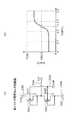
図1(a)は電流源(電流を流す素子)として機能する本発明の第1の実施の形態における半導体素子の回路図を示す。図1(a)において、符号201はNMOSトランジスタを示す。符号202はゲート端子を示す。符号203はドレイン端子を示す。符号204は基板端子を示す。符号Vgはゲート電圧を示す。符号Vdはドレイン電圧を示す。符号Igdはゲート−ドレイン間に流れる電流を示す。(First embodiment)
FIG. 1A is a circuit diagram of a semiconductor element according to the first embodiment of the present invention that functions as a current source (an element through which a current flows). In FIG. 1A,
この半導体素子は、NMOSトランジスタ201の第1の拡散層端子(ドレイン端子)と第2の拡散層端子(ソース端子)とを相互に接続しドレイン端子203とし、基板端子204をドレイン端子203とは分離している。 In this semiconductor element, the first diffusion layer terminal (drain terminal) and the second diffusion layer terminal (source terminal) of the
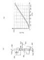
図1(b)は図1(a)の半導体素子(電流源)の電圧−電流特性を示している。横軸には電圧Vg−Vdをとり、縦軸には電流Igdをとっている。同図において、記号Ia、−Iaは任意目盛である。 FIG. 1B shows voltage-current characteristics of the semiconductor element (current source) of FIG. The horizontal axis represents voltage Vg−Vd, and the vertical axis represents current Igd. In the figure, symbols Ia and -Ia are arbitrary scales.
図1のNMOSトランジスタ201においては、ゲート端子202の電圧がドレイン端子203の電圧より高いと、ゲート端子202からドレイン端子203へ電流が流れる。またその時、ゲート端子202とドレイン端子203の電位差がNMOSトランジスタのしきい値電圧を越えると電流は急激に大きくなる。ゲート端子202とドレイン端子203の電位差がNMOSトランジスタのしきい値を越えないとき流れる電流の大きさは、ゲート端子202の電圧がドレイン端子203の電圧より低いときにドレイン端子203からゲート端子202へ電流が流れる電流の大きさと、ゲート端子202とドレイン端子203の電位差が同じであれば同じである。 In the
このように、印加する電圧により発生する電流量を任意に変化することができる。また、この流れる電流の成分はゲートリーク電流であり、その特性は、温度に依存してほとんど変化しない。印加電圧により電流量は変化するが温度に対する依存は少ないため、ある所定の電圧状態下では温度に依存しない電流源として使用することが可能である。 In this way, the amount of current generated by the applied voltage can be changed arbitrarily. The component of the flowing current is a gate leakage current, and its characteristics hardly change depending on the temperature. Although the amount of current varies depending on the applied voltage, the dependence on temperature is small, so that it can be used as a current source independent of temperature under a certain predetermined voltage state.
この半導体素子(電流源)は、図1(c)に示すように、PMOSトランジスタ205を用いることでも同様に作成することができる。図1(c)においては、符号206はゲート端子を示す。符号207はドレイン端子を示す。符号208は基板端子を示す。符号Vgはゲート電圧を示す。符号Vdはドレイン電圧を示す。符号Igdはゲート−ドレイン間に流れる電流を示す。 This semiconductor element (current source) can be similarly formed by using a
図1(d)は図1(c)の半導体素子(電流源)の電圧−電流特性を示している。横軸には電圧Vg−Vdをとり、縦軸には電流Igdをとっている。 FIG. 1D shows the voltage-current characteristics of the semiconductor element (current source) of FIG. The horizontal axis represents voltage Vg−Vd, and the vertical axis represents current Igd.
この実施の形態によれば、温度に依存しない電流を流すことができる。つまり、流れる電流は電圧状態で異なるが、温度に依存しない基準の電流を流し続けることができる。 According to this embodiment, a current independent of temperature can be passed. That is, although the flowing current varies depending on the voltage state, it is possible to continue to flow a reference current that does not depend on temperature.
なお、この実施例で示した素子は、例えば以下のような用途に使用できる。MOSトランジスタはゲート、ドレイン、ソース、および基板に印加される電圧により流れる電流が大きく変わる特徴を持っている。通常はドレイン−ソース間に流れる電流を用いてスイッチとして用いる。本実施の形態の半導体素子は、通常のMOS動作ではない電圧条件と電流特性がある。この特性を使ってスイッチにも用いることは可能と考えられる。また任意の電圧では任意の電流を流すので、抵抗値が変化する抵抗素子として使用することも可能と考えられる。 The element shown in this embodiment can be used for the following applications, for example. The MOS transistor has a characteristic that the current flowing greatly changes depending on the voltage applied to the gate, drain, source and substrate. Usually, it uses as a switch using the electric current which flows between drain-sources. The semiconductor element of the present embodiment has voltage conditions and current characteristics that are not normal MOS operation. It is considered possible to use this characteristic for switches. In addition, since an arbitrary current flows at an arbitrary voltage, it can be considered to be used as a resistance element whose resistance value changes.
(第2の実施の形態)
図2(a)は電流源として機能する本発明の第2の実施の形態における半導体素子の回路図を示す。この半導体素子は、NMOSトランジスタ201の第1の拡散層端子(ドレイン端子)と第2の拡散層端子(ソース端子)と基板端子とを相互に接続しドレイン端子203としている。この実施の形態でも、ゲート端子202とドレイン端子203との間に電流が流れ電流源の特性としては図2(b)に示すように、第1の実施の形態とほぼ同じであり、温度に依存しない素子が得られる。(Second Embodiment)
FIG. 2A is a circuit diagram of a semiconductor element according to the second embodiment of the present invention that functions as a current source. In this semiconductor element, the first diffusion layer terminal (drain terminal), the second diffusion layer terminal (source terminal), and the substrate terminal of the
図2(c)はPMOSトランジスタを用いて電流源として機能する半導体素子を構成したものである。この半導体素子は、PMOSトランジスタ205の第1の拡散層端子(ドレイン端子)と第2の拡散層端子(ソース端子)と基板端子とを相互に接続しドレイン端子207としている。この実施の形態でも、ゲート端子206とドレイン端子207との間に電流が流れ電流源の特性としては図2(d)に示すように、第1の実施の形態とほぼ同じである。 FIG. 2C shows a semiconductor element that functions as a current source using a PMOS transistor. In this semiconductor element, the first diffusion layer terminal (drain terminal), the second diffusion layer terminal (source terminal), and the substrate terminal of the
この半導体素子(電流源)は、シングルゲート構造のトランジスタのみならず、ゲート端子を2つ以上もつマルチゲート構造のトランジスタによっても作成できる。また、SOI構造のトランジスタにおいても作成できる。 This semiconductor element (current source) can be formed not only by a single-gate transistor but also by a multi-gate transistor having two or more gate terminals. It can also be formed in a transistor having an SOI structure.
この実施の形態によれば、第1の実施の形態の実施の形態と同様の効果が得られる。マルチゲートの場合、ゲート面積が大きくすることが容易であり、その場合流れる電流を大きくすることができる。 According to this embodiment, the same effect as that of the first embodiment can be obtained. In the case of a multi-gate, it is easy to increase the gate area, and in that case, the flowing current can be increased.
なお、この実施例で示した素子は、例えば以下のような用途に使用できる。第1の実施の形態(図1)と第2の実施の形態(図2)は基本的にトランジスタの基板が分離されているかどうかが異なる。この素子の用途は第1の実施の形態で示した用途と同じである。基板を分離構造にすることで基板バイアス制御で用いることができる。あとで述べる基板バイアス時のリークモニターには基板が分離されていることが条件となる。 The element shown in this embodiment can be used for the following applications, for example. The first embodiment (FIG. 1) and the second embodiment (FIG. 2) basically differ in whether or not the transistor substrate is separated. The use of this element is the same as that shown in the first embodiment. By making the substrate into a separation structure, it can be used for substrate bias control. It is a condition that the substrate is separated for leak monitoring at the time of substrate bias described later.
(第3の実施の形態)
図3に第3の実施の形態を示す。図3(a)は半導体素子の回路図を示し、同図(b)はこの半導体素子の半導体素子の電圧−電流特性を示し、同図(c)は抵抗の温度特性を示している。(Third embodiment)
FIG. 3 shows a third embodiment. 3A shows a circuit diagram of the semiconductor element, FIG. 3B shows a voltage-current characteristic of the semiconductor element of the semiconductor element, and FIG. 3C shows a temperature characteristic of the resistor.
これは本発明の半導体素子(電流源)を、図3(a)に示すように、抵抗値Rを有する抵抗素子0401として用いるものである。図1の半導体素子において、ゲート端子202とドレイン端子203との間に一定の電圧を印加すると一定の電流が流れるため、この電流源を抵抗素子として用いることができる。 This uses the semiconductor element (current source) of the present invention as a
図3(b)に示すように、印加する電圧により電流が異なることでこの半導体素子からなる抵抗0401は、その抵抗値R(=V/I)が、Ra、Rbと変わっていることが分かる。また、この抵抗0401は、図3(c)に示すように、温度変化による抵抗値変化が非常に小さいので、安定した抵抗素子として用いることができる。また、最低トランジスタ1個で作成できるため、非常に面積の削減に有効である。 As shown in FIG. 3B, it can be seen that the resistance value R (= V / I) of the
なお、図3(a)では、NMOSトランジスタを用いた半導体素子を例にとって説明しているが、PMOSトランジスタを用いた半導体素子についても、同様に抵抗として使用することができる。また、MOSトランジスタの構造についても、シングルゲート構造のトランジスタのみならず、ゲート端子を2つ以上もつマルチゲート構造のトランジスタでもよい。また、SOI構造のトランジスタでもよい。 In FIG. 3A, a semiconductor element using an NMOS transistor is described as an example. However, a semiconductor element using a PMOS transistor can be similarly used as a resistor. Further, the structure of the MOS transistor is not limited to a single-gate transistor, but may be a multi-gate transistor having two or more gate terminals. Alternatively, a transistor having an SOI structure may be used.
この実施の形態によれば、温度に依存しない素子が得られる。 According to this embodiment, an element independent of temperature can be obtained.
この実施の形態の素子は上記実施の形態と同様の用途に使用できる。 The element of this embodiment can be used for the same application as the above embodiment.
(第4の実施の形態)
図4は、本発明の第4の実施の形態に係る半導体集積回路装置のブロック図を示している。(Fourth embodiment)
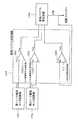
FIG. 4 shows a block diagram of a semiconductor integrated circuit device according to the fourth embodiment of the present invention.
この半導体集積回路装置では、LSI501の中に、MOSトランジスタの基板端子を電源およびグランドから分離した回路ブロック502があり、その回路ブロック502内に温度モニタ回路503が配置されている。そして、LSI501内部には温度判定回路504と基板バイアス発生回路505とが配置されている。 In this semiconductor integrated circuit device, an
温度モニタ回路503は、信号線506により温度判定回路504へ温度モニタ電圧を出力する。温度判定回路504は、温度モニタ電圧に基づいて温度を判定し、信号線507により基板バイアス発生回路505へ温度情報を出力する。そして、所定の基板バイアスを基板バイアス発生回路505で発生し、基板バイアス配線508を通して回路ブロック502の基板へ印加する。 The
これによって、回路ブロック502へ各温度における最適な基板バイアス値を印加することが可能となる。 As a result, an optimum substrate bias value at each temperature can be applied to the
(第5の実施の形態)
図5は、本発明の第5の実施の形態に係る半導体集積回路装置のブロック図を示している。(Fifth embodiment)
FIG. 5 is a block diagram of a semiconductor integrated circuit device according to the fifth embodiment of the present invention.
この半導体集積回路装置では、LSI601の中に、MOSトランジスタの基板端子を電源およびグランドから分離した回路ブロック602があり、その回路ブロック602内に温度モニタ回路603が配置されている。そして、LSI601の外部には温度判定回路604と基板バイアス発生回路605とが配置されている。LSI601の外部に配置するのは、温度判定回路604と基板バイアス発生回路605のうち何れか一方のみでもよい。 In this semiconductor integrated circuit device, an
温度モニタ回路603は、信号線606により温度判定回路604へ温度モニタ電圧を出力する。温度判定回路604は、温度モニタ電圧に基づいて温度を判定し、信号線607により基板バイアス発生回路605へ温度情報を出力する。そして、所定の基板バイアスを基板バイアス発生回路605で発生し、基板バイアス配線608を通して回路ブロック602の基板へ印加する。 The
これによって、回路ブロック602へ各温度における最適な基板バイアス値を印加することが可能となる。 As a result, an optimum substrate bias value at each temperature can be applied to the
(第6の実施の形態)
図6は、本発明の第6の実施の形態に係る半導体集積回路装置のブロック図を示している。(Sixth embodiment)
FIG. 6 is a block diagram of a semiconductor integrated circuit device according to the sixth embodiment of the present invention.
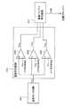
この半導体集積回路装置では、LSI701の中に、MOSトランジスタの基板端子を電源およびグランドから分離した回路ブロック702A,702Bがあり、その回路ブロック702A,702B内に温度モニタ回路703A,703Bがそれぞれ配置されている。そして、LSI701の内部には、温度モニタ回路703A,703Bに対応して温度判定回路704A,704Bと基板バイアス発生回路705A,705Bとが配置されている。温度判定回路704A,704Bと基板バイアス発生回路705A,705Bは、の何れかはLSI701の外部に配置されていてもよい。 In this semiconductor integrated circuit device, the
温度モニタ回路703A,703Bは、信号線706A,706Bにより温度判定回路704A,704Bへ温度モニタ電圧を出力する。温度判定回路704A,704Bは、温度モニタ電圧に基づいて温度を判定し、信号線707A,707Bにより基板バイアス発生回路705A,705Bへ温度情報を出力する。そして、所定の基板バイアスを基板バイアス発生回路705A,705Bで発生し、基板バイアス配線708A,708Bを通して回路ブロック702A,702Bの基板へ印加する。 The
上記のように、LSI701の内部の回路ブロックを2つ以上の回路ブロック702A,702Bに分け、それぞれに対応した温度モニタ回路703A,703B、温度判定回路704A,704B、基板バイアス発生回路705A,705Bを持っても良い。これにより、回路ブロック702A,702Bの違いによる内部温度の違いや、回路ブロック702A,702Bの特性仕上がりを反映し、各回路ブロック702A,702Bへ最適な基板バイアス電圧を印加することが可能であり、低リーク化効果を大きくすることができる。 As described above, the internal circuit block of the
(第7の実施の形態)
図7(a)は、第4、第5および第6の実施の形態における、温度モニタ回路603の詳細な構成を示す回路図である。図7(b)は図7(a)の温度モニタ回路の温度T−出力電圧Vo1の特性図である。温度モニタ回路503,703A,703Bについても、温度モニタ回路603と同様である。(Seventh embodiment)
FIG. 7A is a circuit diagram showing a detailed configuration of the
この温度モニタ回路603は、各々MOSトランジスタからなる2つの半導体素子の直列回路で構成される。第1の半導体素子は、NMOSトランジスタ801のゲート端子、ソース端子および基板端子を相互に接続した構成を有している。また、第2の半導体素子は、NMOSトランジスタ802のドレイン端子、ソース端子および基板端子が相互に接続された構成を有している。 The
そして、NMOSトランジスタ801のドレイン端子は、電源VDD804に接続されている。また、NMOSトランジスタ802のドレイン端子、ソース端子および基板端子はグランドVSS805に接続されている。また、NMOSトランジスタ801のソース端子とNMOSトランジスタ802のゲート端子とが相互に接続され、この接続点が出力端子803となっている。 The drain terminal of the
そして、NMOSトランジスタ801には電流Ioff1が流れ、MOSトランジスタ802には電流Ig1が流れる。これらの電流Ioff1、Ig1が流れることにより、出力端子803に出力電圧として温度モニタ電圧Vo1が現れる。 The current Ioff1 flows through the
図7(b)は温度モニタ回路603の周辺部分の温度と温度モニタ電圧Vo1との関係を示している。同図から、温度に比例して温度モニタ電圧Vo1が増大し、各温度でそれぞれ異なった出力電圧となることがわかる。したがって、出力端子803から出力される温度モニタ電圧Vo1により温度モニタ回路603が置かれた場所の温度を判断することができる。 FIG. 7B shows the relationship between the temperature around the
温度モニタ回路603の原理を、図8を参照しながら説明する。図8(a)には温度モニタ回路603を構成する2つのNMOSトランジスタ801,802を切り離した状態を示している。図8(b)には、両NMOSトランジスタ801,802を流れる電流と温度モニタ出力電圧Vo1との関係、温度と温度モニタ出力電圧Vo1との関係とをそれぞれ示している。 The principle of the
温度モニタ回路603は、NMOSトランジスタ801とNMOS802トランジスタとにより構成される。NMOSトランジスタ801にはドレインリーク電流Ioff1が流れ、NMOSトランジスタ802にはゲートリーク電流Ig1が流れる。その流れる電流量はそれぞれ温度モニタ電圧Vo1の電圧値によって決まり、図8(b)の上図に示すとおりとなる。 The
NMOSトランジスタ801を流れるドレインリーク電流Ioff1とNMOSトランジスタ802を流れるゲートリーク電流Ig1とが等しい電圧になるように、温度モニタ電圧Vo1が固定されるわけであるが、温度が変化するとその温度モニタ電圧Vo1が図8(b)の下図に示すように変化する。 The temperature monitor voltage Vo1 is fixed so that the drain leak current Ioff1 flowing through the
これは、NMOSトランジスタ802を流れるゲートリーク電流Ig1は温度によりほとんど変化しないものの、NMOSトランジスタ801を流れるドレインリーク電流Ioff1は温度が上昇すると急激に大きくなるためである。したがって、温度が低いとき、温度モニタ電圧Vo1は低くなり、温度が高いとき温度モニタ電圧Vo1は高くなり、各温度でそれぞれ異なった温度モニタ電圧Vo1が出力される。これにより、上記温度モニタ回路603としての役割を果たすことができる。 This is because the gate leakage current Ig1 flowing through the
図9は温度判定回路604の構成を示すブロック図である。温度判定回路604は、温度を比較するための1個以上のオペアンプを備えている。本実施の形態では、3個のオペアンプ1001〜1003を備えている。ただし、オペアンプの数はいくつであっても構わない。温度モニタ回路603から出力された温度モニタ電圧Vo1は、温度判定回路604内の全てのオペアンプ1001〜1003に入力される。このとき、それぞれのオペアンプ1001〜1003のリファレンス電圧VREFには、各温度における温度モニタ回路604の出力電圧に相当する電圧が印加されている。例えば、0℃の時にはVia(0℃判定基準値)が印加され、25℃の時にはVib(25℃判定基準値)が印加され、Vic(50℃判定基準値)が印加される。そして、実際の温度モニタ回路603からの出力である温度モニタ電圧Vo1との大小を判定し、その判定結果を基板バイアス発生回路605へ入力する。そして、その判定結果により、モニタしているときの温度を判定することが可能となり、設定した各温度でのリーク電流を最小にするために最適な基板バイアス電圧を内部の回路ブロック602へ印加することができる。 FIG. 9 is a block diagram illustrating a configuration of the
図10は、各温度における温度モニタ回路603の温度モニタ電圧Vo1、温度判定回路604内のオペアンプ1001〜1003の出力Voa,Vob,Voc、そして回路ブロック602に印加される基板バイアスVBPの関係を示す。このように、温度モニタ電圧Vo1に基づいて出力Voa、Vob、Vocが決定され、出力Voa、Vob、Vocに基づいて各温度によって最適な基板バイアス値VBPを、Vα、Vβ、Vγ、Vδのように、容易に選択することが可能となる。また、温度モニタ回路603は最小でトランジスタを2個のみ使ったものであり、小面積かつ容易に作成できる。 FIG. 10 shows the relationship between the temperature monitor voltage Vo1 of the
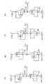
図11(a)〜(d)に温度モニタ回路603の別の例を示す。温度モニタ回路603はNMOSトランジスタのみではなく、図11(a)に示すようにPMOSトランジスタのみで作ることも可能である。また、図11(b)に示すように、第1のトランジスタと第2のトランジスタの配置をVDD側とVSS側で入れ替えることが可能である。また、図11(c)に示すように、ゲートリーク電流を流す第2のトランジスタは出力端子803とVSSに接続する端子とを入れ替えても良い。そして、図11(d)に示すように、NMOSトランジスタ、PMOSトランジスタをそれぞれ組み合わせて作ることもできる。これらの時には、それぞれの温度と温度モニタ電圧Vo1の関係を鑑み、温度判定回路604の構成を変更するだけでよい。 FIGS. 11A to 11D show another example of the
(第8の実施の形態)
次に、温度モニタ回路603の別の実施の形態を説明する。(Eighth embodiment)
Next, another embodiment of the
なお、本実施の形態で説明する温度モニタ回路603は、第4、5、6の実施の形態で説明した半導体集積回路装置に適用することができる。 Note that the
温度モニタ回路603の出力電圧Vo1は、図12に示すように、ゲートリーク電流Igとドレインリーク電流Ioffとの関係で決まっており、ゲートリーク電流Igとドレインリーク電流Ioffとが釣り合う電圧が温度モニタVo1として出力される。したがって、ゲートリーク電流Igもしくはドレインリーク電流Ioffの特性を変更することで、温度モニタ電圧Vo1を変えることができる。 As shown in FIG. 12, the output voltage Vo1 of the
そして、ある温度の時の温度モニタ電圧Vo1の値を任意の電圧(例えばVDD/2)に設定することができる。 The value of the temperature monitor voltage Vo1 at a certain temperature can be set to an arbitrary voltage (for example, VDD / 2).
例えば、図12において、ゲートリーク電流Ig1とドレインリーク電流Ioff1との組み合わせでは、温度モニタ電圧Vo1が電圧Vaとなるが、ゲートリーク電流Ig1からゲートリーク電流Ig2に設定を変更し、ゲートリーク電流Ig2とドレインリーク電流Ioff1の組み合わせにすると、温度モニタ電圧Vo1がVDD/2に変化する。 For example, in FIG. 12, in the combination of the gate leakage current Ig1 and the drain leakage current Ioff1, the temperature monitor voltage Vo1 becomes the voltage Va, but the setting is changed from the gate leakage current Ig1 to the gate leakage current Ig2, and the gate leakage current Ig2 And the drain leakage current Ioff1, the temperature monitor voltage Vo1 changes to VDD / 2.
同様にして、ドレインリーク電流Ioff1をドレインリーク電流Ioff2に設定を変更してゲートリーク電流Ig1とドレインリーク電流Ioff2の組み合わせにすると、温度モニタ電圧Vo1がVDD/2に変化する。 Similarly, when the setting of the drain leakage current Ioff1 is changed to the drain leakage current Ioff2 to make a combination of the gate leakage current Ig1 and the drain leakage current Ioff2, the temperature monitor voltage Vo1 changes to VDD / 2.
この考え方を用いて、各温度に応じて各温度モニタ回路を設計することにより、図13に示すように各温度の時に温度モニタ電圧Vo1が同じ電圧VDD/2となる3種類の温度モニタ回路A,B,Cを作ることができる。 By designing each temperature monitor circuit according to each temperature using this concept, as shown in FIG. 13, three types of temperature monitor circuits A in which the temperature monitor voltage Vo1 becomes the same voltage VDD / 2 at each temperature are shown. , B, C can be made.
この温度モニタ回路A,B,Cを用いたときの温度判定回路は図14のようになる。図14において、温度判定回路1504内には複数の温度モニタ回路1501,1502,1503に対応した同じ数のオペアンプ1505,1506,1507が内蔵されている。そして、各温度の時に温度モニタ電圧Vo1,Vo2,Vo3がVDD/2になるように設定した温度モニタ回路1501,1502,1503の出力がそれぞれに対応したオペアンプ1505,1506,1507に入力される。このときオペアンプ1505,1506,1507のリファレンス電圧VREFには一律でVDD/2が入力されている。そして、それぞれのオペアンプ1505,1506,1507の出力を基板バイアス発生回路1508に入力し、各温度で最適な基板バイアス電圧を回路ブロックに印加する。 FIG. 14 shows a temperature determination circuit when the temperature monitor circuits A, B, and C are used. In FIG. 14, the same number of
図15は各温度における温度モニタ回路1501,1502,1503の出力電圧Vo1、Vo2、Vo3、温度判定回路1504内のオペアンプ出力Voa,Vob,Voc、そして回路ブロック602に印加される基板バイアスの関係を示す。この図から分かるように、各温度によって最適な基板バイアス値を容易に選択することができる。また、温度モニタ回路603は最小でトランジスタを2個のみ使ったものであり、小面積かつ容易に作成できる。 FIG. 15 shows the relationship between the output voltages Vo1, Vo2, and Vo3 of the
(第9の実施の形態)
次に、半導体集積回路装置の別の実施の形態を説明する。(Ninth embodiment)
Next, another embodiment of the semiconductor integrated circuit device will be described.
図16は、本発明の第9の実施に係る実施の形態における半導体集積回路装置の構成を示すブロック図である。この半導体集積回路装置は、LSI1701の内部にトランジスタの基板端子を電源およびグランドから分離した回路ブロック1702があり、その中に第1リーク電流モニタ回路部1703および第2リーク電流モニタ回路部1704を備える。そして、LSI1701の内部には基板バイアス決定回路1705と基板バイアス発生回路1706とを備える。 FIG. 16 is a block diagram showing a configuration of a semiconductor integrated circuit device according to the ninth embodiment of the present invention. This semiconductor integrated circuit device includes a
第1リーク電流モニタ回路部1703の出力が信号線1707を通り基板バイアス決定回路1705に入力され、第2リーク電流モニタ回路部1704の出力が信号線1708を通り基板バイアス決定回路1705に入力される。そして、基板バイアス決定回路1705の出力が信号線1709を通り基板バイアス発生回路1706に入力され、各状態に応じた最適な基板バイアス電圧が電源配線1710を通じて回路ブロック1702に印加される。 The output of the first leak current
図17に別の実施の形態を示す。これは、基板バイアス決定回路1705と基板バイアス発生回路1706をLSI1701の外に配置した形となっている。回路の動作としては図16に記載の実施の形態と同様である。なお、LSI1701の外に配置するのは、基板バイアス決定回路1705と基板バイアス発生回路1706の何れか一方だけでもよい。 FIG. 17 shows another embodiment. In this configuration, a substrate
図18に別の実施の形態を示す。これはLSI1701内部の回路ブロックを2つ以上の回路ブロック1702A,1702Bに分け、それぞれに対応した第1リーク電流モニタ回路部1703A、1703B、第2リーク電流モニタ回路部1704A、1704Bと、基板バイアス決定回路1705A,1705B、基板バイアス発生回路1706A、1706Bを持つ構造である。 FIG. 18 shows another embodiment. In this circuit, the circuit block in the
そして、第1リーク電流モニタ回路部1703A、1703Bの出力が信号線1707A、1707Bを通り基板バイアス決定回路1705A、1705Bに入力され、第2リーク電流モニタ回路部1704A、1704Bの出力が信号線1708A、1708Bを通り基板バイアス決定回路1705A、1705Bに入力される。そして、基板バイアス決定回路1705A、1705Bの出力が信号線1709A,1709Bを通り基板バイアス発生回路1706A、1706Bに入力され、各状態に応じた最適な基板バイアス電圧が電源配線1710A、1710Bを通じて回路ブロック1702A,1702Bに印加される。 The outputs of the first leak current monitor circuit units 1703A and 1703B are input to the substrate
これにより、回路ブロックの違いによる特性仕上がりを反映し、より各回路ブロック1702A,1702Bへ最適な基板バイアス電圧を印加することが可能であり、低リーク化効果を大きくすることができる。 As a result, it is possible to apply the optimum substrate bias voltage to each of the circuit blocks 1702A and 1702B, reflecting the characteristic finish due to the difference between the circuit blocks, and to increase the effect of reducing leakage.
第1リーク電流モニタ回路部1703を図19(a)に示す。この第1リーク電流モニタ回路部1703はドレインリーク電流の基板バイアス依存性から最適な基板バイアス値を決定するものである。 The first leakage current
第1リーク電流モニタ回路部1703は、NMOSトランジスタ2001,2002で構成されている。NMOSトランジスタ2001は、ドレインが電源VDD2003に接続され、ゲートとソースが接続されている。NMOSトランジスタはゲートとソースがグランドVSS2003に接続されている。そして、NMOSトランジスタ2001のソースとNMOSトランジスタ2002のドレインとが接続され出力端子2006となっている。NMOSトランジスタ2001とNMOSトランジスタ2002の基板は共通の基板端子2005に接続されている。NMOSトランジスタ2001とNMOSトランジスタ2002は同じ仕様であり、ドレイン、ゲート、ソース、基板にそれぞれ同一の電位を印加したときは同一のリーク電流を流すトランジスタとする。このとき基板バイアスVBPと出力端子2006から出力される電圧Vo1との関係は図19(b)に示す通りである。あるVBP電圧Vαを越えると、電圧Vo1はVDD/2以下からVDD/2以上に変化する。このVBP電圧Vαがリーク電流を削減する最適な基板バイアス電圧となる。 The first leakage current
図20を参照して第1リーク電流モニタ回路部1703の原理を説明する。図20(a)にはNMOSトランジスタ2001,2002を切り離した状態の回路図を示している。図20(b)には、基板バイアス電圧VBPと各NMOSトランジスタ2001,2002に流れるドレインリーク電流Ioff1,Ioff2を示している。 The principle of the first leak current
NMOSトランジスタ2001およびNMOSトランジスタ2002の電圧Vo1に同じ電圧を印加していると仮定した場合、基板バイアス電圧VBPとリーク電流の特性は図20(b)に示すとおりである。NMOSトランジスタ2001とNMOSトランジスタ2002は同一の仕様であるが、電源VDDとグランドVSS間に縦積みに配置されているためNMOSトランジスタ2001はNMOSトランジスタ2002より大きめの基板バイアス電圧が印加されることとなる。 Assuming that the same voltage is applied to the voltage Vo1 of the
ドレインリーク電流は基板バイアス電圧VBPを大きくしていくと減少する。しかし、ある電圧Vα以上印加すると、ドレインリーク電流は増加する。したがって、基板バイアス電圧VBPがVαまでは基板バイアスが大きめに掛かるNMOSトランジスタ2001の方はリーク電流が少ない。しかし、Vαを越える領域となると基板バイアス電圧VBPが大きめに掛かるNMOSトランジスタ2001の方はリーク電流が大きくなる。結局、第1リーク電流モニタ回路部1703の出力電圧Vo1は、NMOSトランジスタ2001とNMOSトランジスタ2002とに流れるリーク電流が等しくなる電圧になる。従って、基板バイアス電圧VBPを変化させたときの、出力電圧Vo1は図21(b)に示すようになる。図21(b)の上図には、基板バイアス電圧VBPをパラメータとする電圧Vo1とドレインリーク電流Ioff1,Ioff2の関係を示している。また、図21(b)の下図には、ドレインリーク電流Ioff1,Ioff2が等しくなる状態における電圧Vo1と基板バイアス電圧VBPの関係を示している。なお、図21(a)は図20(a)と同じである。 The drain leakage current decreases as the substrate bias voltage VBP is increased. However, when a voltage Vα or higher is applied, the drain leakage current increases. Therefore, the leakage current is smaller in the
基板バイアス電圧VBPがドレインリーク電流を最小値にするVα以下の時、電圧Vo1はVDD/2以下となり、Vα以上に基板バイアスVBPの値を上げると、電圧Vo1はVDD/2以上となる。このように、第1リーク電流モニタ回路部1703の出力が最適な基板バイアスVαの時、VDD/2となる。 When the substrate bias voltage VBP is equal to or lower than Vα at which the drain leakage current is minimized, the voltage Vo1 is equal to or lower than VDD / 2. When the substrate bias VBP is increased above Vα, the voltage Vo1 becomes equal to or higher than VDD / 2. Thus, when the output of the first leakage current
つぎに、第2リーク電流モニタ回路部1704を説明する。この第2リーク電流モニタ回路部1704はドレインリーク電流の基板バイアス依存性とゲートリーク電流との関係で最適な基板バイアス値を決定するものである。図22(a)にその構成を示す。この第2リーク電流モニタ回路部1704は、第1のNMOSトランジスタ2301および第2のNMOSトランジスタ2302で構成されている。第1のNMOSトランジスタ2301は、ドレインが電源VDD2303に接続され、ゲートとソースが接続されている。第2のNMOSトランジスタ2302のドレインとソースはグランドVSS2304に接続され、第1のNMOSトランジスタ2301のソースと第2のNMOSトランジスタ2302のゲートとが接続され出力端子2306となっている。そして、第1のNMOSトランジスタ2301と第2のNMOSトランジスタ2302の基板は基板端子2305に接続されている。基板バイアスVBPと出力端子2306の出力電圧Vo2との関係は図22(b)に示すとおりであり、リーク電流を最大に削減する最適基板バイアス電圧VβのときVo2はVDD/2となる。 Next, the second leakage current
図23を参照して第2リーク電流モニタ回路部1704の原理を説明する。図23(a)は、NMOSトランジスタ2301,2302を切り離した状態の回路図を示している。図23(b)には基板バイアス電圧VBPと各NMOSトランジスタ2301,2302に流れるドレインリーク電流Ioff1およびゲートリーク電流Ig1を示している。 The principle of the second leakage current
NMOSトランジスタ2301とNMOSトランジスタ2302にそれぞれ同じ基板バイアスが印加されている。NMOSトランジスタ2301を流れるドレインリーク電流Ioff1は基板バイアスVBPの印加で大きく変化する。しかし、NMOSトランジスタ2302を流れるゲートリーク電流Ig1は基板バイアスVBPを変化させてもほとんど変化しない。このNMOSトランジスタ2301を流れるドレインリーク電流Ioff1とNMOSトランジスタ2302を流れるゲートリーク電流Ig1とが等しくなるように出力電圧Vo2が決まる。 The same substrate bias is applied to the
基板バイアスVBPが小さいときNMOSトランジスタ2301を流れるドレインリーク電流Ioff1がNMOSトランジスタ2302を流れるゲートリーク電流Ig1より大きいため、出力電圧Vo2はVDD/2以上となる。しかし、ある基板バイアス値Vβまで基板バイアス電圧VBPを大きくすると、NMOSトランジスタ2301を流れるドレインリーク電流Ioff1の方がNMOSトランジスタ2302を流れるゲートリーク電流Ig1より小さくなるため、出力電圧Vo2はVDD/2以下となる。 Since the drain leakage current Ioff1 flowing through the
図24(b)に基板バイアスVBPの変化と出力電圧Vo2の関係を示す。図24(b)の上図には、基板バイアス電圧VBPをパラメータとする電圧Vo2とドレインリーク電流Ioff1およびゲートリーク電流Ig1の関係を示している。また、図24(b)の下図には、ドレインリーク電流Ioff1とゲートリーク電流Ig1とが等しくなる状態における電圧Vo2と基板バイアス電圧VBPの関係を示している。このように最適な基板バイアス値Vβの時、電圧Vo2はVDD/2となる。図24(a)は図23(b)と同じである。 FIG. 24B shows the relationship between the change in the substrate bias VBP and the output voltage Vo2. The upper diagram of FIG. 24B shows the relationship between the voltage Vo2 using the substrate bias voltage VBP as a parameter, the drain leakage current Ioff1, and the gate leakage current Ig1. The lower diagram of FIG. 24B shows the relationship between the voltage Vo2 and the substrate bias voltage VBP when the drain leakage current Ioff1 and the gate leakage current Ig1 are equal. Thus, at the optimum substrate bias value Vβ, the voltage Vo2 is VDD / 2. FIG. 24A is the same as FIG.
図25は基板バイアス決定回路1705の構成を示すブロック図である。基板バイアス決定回路1705の内部にはオペアンプ2601、オペアンプ2602、オペアンプ2603が備えられ、第1リーク電流モニタ回路部1703とオペアンプ2601、第2リーク電流モニタ回路部1704とオペアンプ2602が対応するようになっている。そして、第1リーク電流モニタ回路部1703の出力電圧Vo1がオペアンプ2601に入力される。このとき、オペアンプ2601のリファレンス電圧VREFとしてはVDD/2が印加されている。第2リーク電流モニタ回路部1704の出力電圧Vo2はオペアンプ2602にリファレンス電圧VREFとして入力される。このとき、オペアンプ2602の入力にはVDD/2が印加されている。そして、オペアンプの出力Voa、Vobが基板バイアス発生回路1706に入力される。第1のリーク電流モニタ回路1703はドレインリーク電流が最小になったときに、VDD/2が出力される構成になっている。この特性を活かしてドレインリーク電流が最小になるまで基板バイアス電圧を増加しドレインリーク電流が最小になった段階で基板バイアス電圧の増加を止める。第2のリーク電流モニタ回路1704はドレインリーク電流とゲートリーク電流の大きさが同じになったときに、VDD/2が出力される構成になっている。この特性を活かしてドレインリーク電流がゲートリーク電流と同じ電流になるまで基板バイアス電圧を増加しドレインリーク電流がゲートリーク電流と同じ電流になった段階で基板バイアス電圧の増加を止める。この構成によりリーク電流の削減に最適な基板バイアス電圧状態を決定できる。そして、基板バイアス発生回路1706の内部で発生した基板バイアス電圧が回路ブロック1702に印加される。また、基板バイアス発生回路1706から出力された基板バイアス電圧VBPはオペアンプ2603に入力され、オペアンプ2603のリファレンス電圧VREFには基板バイアス印加限界基準値となる電圧Vγを印加する。これにより、基板バイアスが大きくなりすぎてデバイス耐圧を越えることを防ぐ。 FIG. 25 is a block diagram showing a configuration of the substrate
図26に各条件における基板バイアス制御の動きを示す。このようにして、回路ブロック1702へリーク電流を最も削減しかつデバイス耐圧を越えない最適な基板バイアス電圧を印加することができる。 FIG. 26 shows the movement of the substrate bias control under each condition. In this way, an optimum substrate bias voltage that reduces the leakage current most and does not exceed the device breakdown voltage can be applied to the
第1リーク電流モニタ回路部、第2のリーク電流モニタ回路は、それぞれNMOSトランジスタ、PMOSトランジスタ用として、構成される。 The first leak current monitor circuit unit and the second leak current monitor circuit are configured for NMOS transistors and PMOS transistors, respectively.
図27(a),(b)にはPMOSトランジスタ用の第1リーク電流モニタ回路部、および第2リーク電流モニタ回路部が示されている。基板バイアス決定回路はPMOSトランジスタの特性に応じて変更される。図27(a)において、符号2401,2402,2501,2502はそれぞれPMOSトランジスタを示す。 FIGS. 27A and 27B show a first leak current monitor circuit section and a second leak current monitor circuit section for the PMOS transistor. The substrate bias determination circuit is changed according to the characteristics of the PMOS transistor. In FIG. 27A,
図28(a)に別の形態の第2リーク電流モニタ回路部1704を示す。これは、電源とグランドの間に配置される第1のNMOSトランジスタ2301と第2のNMOSトランジスタ2302の位置を入れ替えた構造となっている。このとき、出力端子Vo2から出力される電圧の特性も変化するので基板バイアス決定回路1705の構成を変更する必要がある。 FIG. 28A shows another type of second leakage current
図28(b)には、PMOSトランジスタにおいて上記と同様に第1のPMOSトランジスタと第2のPMOSトランジスタを入れ替えた構成を示している。 FIG. 28B shows a configuration in which the first PMOS transistor and the second PMOS transistor are interchanged in the PMOS transistor in the same manner as described above.
本発明に係る半導体集積回路装置は、ドレイン端子とソース端子とを共通接続したMOSトランジスタからなる半導体素子を基板制御回路の基板バイアス電圧を決定するモニタ制御回路に活用することで、低消費電力な半導体集積回路装置を実現することができる。 The semiconductor integrated circuit device according to the present invention uses a semiconductor element formed of a MOS transistor having a drain terminal and a source terminal connected in common to a monitor control circuit that determines a substrate bias voltage of the substrate control circuit, thereby reducing power consumption. A semiconductor integrated circuit device can be realized.
101 PMOSトランジスタ
102 NMOSトランジスタ
103 Nウエル基板端子
104 電源端子
105 インバータ回路の入力端子
106 グランド端子
107 Pウエル基板端子
108 インバータ回路の出力端子
201 NMOSトランジスタ
202 ゲート端子
203 ドレイン端子
204 基板端子
205 PMOSトランジスタ
206 ゲート端子
207 ドレイン端子
208 基板端子
401 抵抗素子
501 LSI
502 回路ブロック
503 温度モニタ回路
504 温度判定回路
505 基板バイアス発生回路
506 信号線
507 信号線
508 基板バイアス配線
601 LSI
602 回路ブロック
603 温度モニタ回路
604 温度判定回路
605 基板バイアス発生回路
606 信号線
607 信号線
608 基板バイアス配線
801 第1のNMOSトランジスタ
802 第2のNMOSトランジスタ
803 出力端子
804 電源端子
805 グランド端子
1001 0℃判定用オペアンプ
1002 25℃判定用オペアンプ
1003 50℃判定用オペアンプ
1501 0℃用温度モニタ回路
1502 25℃用温度モニタ回路
1503 50℃用温度モニタ回路
1504 温度判定回路
1505 オペアンプ
1506 オペアンプ
1507 オペアンプ
1701 LSI
1702 回路ブロック
1703 第1リーク電流モニタ回路部
1704 第2リーク電流モニタ回路部
1705 基板バイアス決定回路
1706 基板バイアス発生回路
1707 信号線
1708 信号線
1709 信号線
1710 基板バイアス配線
2001 第1のNMOSトランジスタ
2002 第2のNMOSトランジスタ
2003 電源端子
2004 グランド端子
2005 基板端子
2006 出力端子
2301 第1のNMOSトランジスタ
2302 第2のNMOSトランジスタ
2303 電源端子
2304 グランド端子
2305 基板端子
2306 出力端子
2601 オペアンプ
2602 オペアンプ
2603 オペアンプ101
502
602
1702
Claims (32)
Translated fromJapanese前記温度モニタ回路の出力をもとに前記温度判定回路で前記回路ブロックの温度を判定し、前記温度判定回路の判定出力を前記基板バイアス発生回路へ入力することにより、前記回路ブロックの温度に応じた基板バイアスを前記基板バイアス発生回路から前記回路ブロックの前記第1のMOSトランジスタの基板端子へ印加する半導体集積回路装置であって、
前記温度モニタ回路は、第1および第2の半導体素子の直列回路からなり、
前記第1の半導体素子は第2のMOSトランジスタのソース端子とゲート端子と基板端子とが相互に接続された構造を有し、前記第2のMOSトランジスタのドレイン端子が一端となり、前記第2のMOSトランジスタのソース端子が他端となり、
前記第2の半導体素子は第3のMOSトランジスタのドレイン端子とソース端子と基板端子とが相互に接続された構造を有し、前記第3のMOSトランジスタのゲート端子が一端となり、前記第3のMOSトランジスタの第1の拡散層端子が他端となり、
前記第1および第2の半導体素子の直列回路に電圧が印加されることにより、前記第1および第2の半導体素子の接続点から前記回路ブロックの温度に応じた信号を出力する半導体集積回路装置。A circuit block including a first MOS transistor, wherein a substrate terminal of the first MOS transistor is separated from a power supply terminal and a ground terminal; a temperature monitor circuit provided in the circuit block; a temperature determination circuit; and a substrate bias Generator circuit,
The temperature determination circuit determines the temperature of the circuit block based on the output of the temperature monitor circuit, and the determination output of the temperature determination circuit is input to the substrate bias generation circuit, so that the temperature of the circuit block is determined. Applying a substrate bias from the substrate bias generation circuit to a substrate terminal of the first MOS transistor of the circuit block,
The temperature monitor circuit comprises a series circuit of first and second semiconductor elements,
The first semiconductor element has a structure in which a source terminal, a gate terminal, and a substrate terminal of a second MOS transistor are connected to each other, and a drain terminal of the second MOS transistor serves as one end. The source terminal of the MOS transistor is the other end,
The second semiconductor element has a structure in which a drain terminal, a source terminal, and a substrate terminal of a third MOS transistor are connected to each other, and a gate terminal of the third MOS transistor serves as one end. The first diffusion layer terminal of the MOS transistor is the other end,
A semiconductor integrated circuit device that outputs a signal corresponding to the temperature of the circuit block from a connection point of the first and second semiconductor elements by applying a voltage to a series circuit of the first and second semiconductor elements. .
前記温度判定回路は1個以上のオペアンプで構成され、前記温度モニタ回路の出力が前記オペアンプに入力され、前記オペアンプの出力が前記基板バイアス発生回路へ入力され、それぞれの前記オペアンプのリファレンス電圧にはそれぞれ異なった電位が入力され、それぞれのリファレンス電圧の電位は前記温度モニタ回路の所定の温度状態における出力に相当する電位である請求項17記載の半導体集積回路装置。The second MOS transistor and the third MOS transistor are respectively composed of a first NMOS transistor and a second NMOS transistor. The drain terminal of the first NMOS transistor is fixed at a power supply potential, and the second NMOS transistor is a drain. The terminal is fixed to the ground potential, the source terminal of the first NMOS transistor and the gate terminal of the second NMOS transistor are connected, and the gate terminal of the second NMOS transistor becomes the output terminal of the temperature monitoring circuit. ,
The temperature determination circuit is composed of one or more operational amplifiers, the output of the temperature monitor circuit is input to the operational amplifier, the output of the operational amplifier is input to the substrate bias generation circuit, and the reference voltage of each operational amplifier is 18. The semiconductor integrated circuit device according to claim 17, wherein different potentials are input, and the potential of each reference voltage is a potential corresponding to an output of the temperature monitor circuit in a predetermined temperature state.
前記温度判定回路は1個以上のオペアンプで構成され、前記温度モニタ回路の出力が前記オペアンプに入力され、前記オペアンプの出力が前記基板バイアス発生回路へ入力され、それぞれの前記オペアンプのリファレンス電圧にはそれぞれ異なった電位が入力され、それぞれのリファレンス電圧の電位は前記温度モニタ回路の所定の温度状態における出力に相当する電位である請求項17記載の半導体集積回路装置。The second MOS transistor and the third MOS transistor are respectively composed of first and second PMOS transistors, the source terminal of the first PMOS transistor is fixed at a power supply potential, and the second PMOS transistor is The drain terminal is fixed to the ground potential, the drain terminal of the first PMOS transistor and the gate terminal of the second PMOS transistor are connected, and the gate terminal of the second PMOS transistor is the output terminal of the temperature monitor circuit And
The temperature determination circuit is composed of one or more operational amplifiers, the output of the temperature monitor circuit is input to the operational amplifier, the output of the operational amplifier is input to the substrate bias generation circuit, and the reference voltage of each operational amplifier is 18. The semiconductor integrated circuit device according to claim 17, wherein different potentials are input, and the potential of each reference voltage is a potential corresponding to an output of the temperature monitor circuit in a predetermined temperature state.
前記回路ブロック内に前記温度モニタ回路を2個以上備え、前記温度モニタ回路はそれぞれ異なった温度の時に出力が電源電圧の1/2になるように、前記第1および第2のNMOSトランジスタが調整され、
前記温度判定回路は前記温度モニタ回路と同数のオペアンプで構成され、前記温度モニタ回路の出力がそれぞれ対となる前記オペアンプに入力され、前記オペアンプの出力が前記基板バイアス発生回路へ入力され、それぞれの前記オペアンプのリファレンス電圧には電源電圧の1/2の電圧が入力される請求項17記載の半導体集積回路装置。The second MOS transistor and the third MOS transistor are respectively composed of a first NMOS transistor and a second NMOS transistor. The drain terminal of the first NMOS transistor is fixed at a power supply potential, and the second NMOS transistor is a drain. The terminal is fixed to the ground potential, the source terminal of the first NMOS transistor and the gate terminal of the second NMOS transistor are connected, and the gate terminal of the second NMOS transistor becomes the output terminal of the temperature monitoring circuit. ,
Two or more temperature monitoring circuits are provided in the circuit block, and the first and second NMOS transistors are adjusted so that the output becomes half of the power supply voltage at different temperatures. And
The temperature determination circuit is composed of the same number of operational amplifiers as the temperature monitoring circuit, and the outputs of the temperature monitoring circuits are input to the paired operational amplifiers, and the outputs of the operational amplifiers are input to the substrate bias generation circuit. 18. The semiconductor integrated circuit device according to claim 17, wherein a voltage that is ½ of a power supply voltage is input to the reference voltage of the operational amplifier.
前記回路ブロック内に前記温度モニタ回路を2個以上備え、前記温度モニタ回路はそれぞれ異なった温度の時に出力が電源電圧の1/2になるように、前記第1および第2のPMOSトランジスタが調整され、
前記温度判定回路は前記温度モニタ回路と同数のオペアンプで構成され、前記温度モニタ回路の出力がそれぞれ対となる前記オペアンプに入力され、前記オペアンプの出力が前記基板バイアス発生回路へ入力され、それぞれの前記オペアンプのリファレンス電圧には電源電圧の1/2の電圧が入力される請求項17記載の半導体集積回路装置。The second MOS transistor and the third MOS transistor are respectively composed of first and second PMOS transistors, the source terminal of the first PMOS transistor is fixed at the power supply potential, and the second PMOS transistor is the drain. The terminal is fixed to the ground potential, the drain terminal of the first PMOS transistor and the gate terminal of the second PMOS transistor are connected, and the gate terminal of the second PMOS transistor becomes the output terminal of the temperature monitoring circuit. ,
Two or more temperature monitoring circuits are provided in the circuit block, and the first and second PMOS transistors are adjusted so that the output becomes half of the power supply voltage at different temperatures. And
The temperature determination circuit is composed of the same number of operational amplifiers as the temperature monitoring circuit, and the outputs of the temperature monitoring circuits are input to the paired operational amplifiers, and the outputs of the operational amplifiers are input to the substrate bias generation circuit. 18. The semiconductor integrated circuit device according to claim 17, wherein a voltage that is ½ of a power supply voltage is input to the reference voltage of the operational amplifier.
前記リーク電流モニタ回路の出力をもとに前記基板バイアス決定回路で前記回路ブロックのリーク電流に応じて基板バイアスを決定し、前記基板バイアス決定回路の出力を前記基板バイアス発生回路へ入力することにより、前記回路ブロックのリーク電流に応じた基板バイアスを前記基板バイアス発生回路から前記回路ブロックの前記第1のMOSトランジスタの基板端子へ印加する半導体集積回路装置であって、
前記リーク電流モニタ回路は、第1のリーク電流モニタ回路部と第2のリーク電流モニタ回路部とからなり、
前記第1のリーク電流モニタ回路部が第1および第2の半導体素子の直列回路からなり、前記第2のリーク電流モニタ回路部が第3および第4の半導体素子の直列回路からなり、
前記第1の半導体素子が第2のMOSトランジスタのソース端子とゲート端子とが相互に接続された構造を有し、前記第2のMOSトランジスタのドレイン端子が一端となり、前記第2のMOSトランジスタのソース端子とが他端となり、
前記第2の半導体素子が第3のMOSトランジスタのソース端子とゲート端子とが相互に接続された構造を有し、前記第3のMOSトランジスタのドレイン端子が一端となり、前記第3のMOSトランジスタのソース端子が他端となり、
前記第3の半導体素子が第4のMOSトランジスタのソース端子とゲート端子とが相互に接続された構造を有し、前記第4のMOSトランジスタのドレイン端子が一端となり、前記第4のMOSトランジスタのソース端子が他端となり、
前記第4の半導体素子が第5のMOSトランジスタのドレイン端子とソース端子とが相互に接続された構造を有し、前記第5のMOSトランジスタのゲート端子が一端となり、前記第5のMOSトランジスタのドレイン端子が他端となり、
前記第2のMOSトランジスタの基板端子と前記第3のMOSトランジスタの基板端子とが相互に接続され、かつ前記第1のMOSトランジスタの基板端子に接続され、
前記第4のMOSトランジスタの基板端子と前記第5のMOSトランジスタの基板端子とが相互に接続され、かつ前記第1のMOSトランジスタの基板端子に接続され、
前記第1および第2の半導体素子の直列回路に電圧が印加されることにより、前記第1および第2の半導体素子の接続点から前記回路ブロックのリーク電流に応じた第1の信号を出力し、
前記第3および第4の半導体素子の直列回路に電圧が印加されることにより、前記第3および第4の半導体素子の接続点から前記回路ブロックのリーク電流に応じた第2の信号を出力する半導体集積回路装置。A circuit block including a first MOS transistor, wherein a substrate terminal of the first MOS transistor is separated from a power supply terminal and a ground terminal; a leakage current monitor circuit provided in the circuit block; a substrate bias determination circuit; A substrate bias generation circuit,
By determining the substrate bias according to the leakage current of the circuit block by the substrate bias determination circuit based on the output of the leakage current monitor circuit, and inputting the output of the substrate bias determination circuit to the substrate bias generation circuit A semiconductor integrated circuit device for applying a substrate bias according to a leakage current of the circuit block from the substrate bias generation circuit to a substrate terminal of the first MOS transistor of the circuit block,
The leak current monitor circuit includes a first leak current monitor circuit unit and a second leak current monitor circuit unit,
The first leakage current monitor circuit section is composed of a series circuit of first and second semiconductor elements, and the second leakage current monitor circuit section is composed of a series circuit of third and fourth semiconductor elements;
The first semiconductor element has a structure in which a source terminal and a gate terminal of a second MOS transistor are connected to each other, a drain terminal of the second MOS transistor serves as one end, and The source terminal is the other end,
The second semiconductor element has a structure in which a source terminal and a gate terminal of a third MOS transistor are connected to each other, a drain terminal of the third MOS transistor serves as one end, and The source terminal becomes the other end,
The third semiconductor element has a structure in which a source terminal and a gate terminal of a fourth MOS transistor are connected to each other, a drain terminal of the fourth MOS transistor serves as one end, and the fourth MOS transistor The source terminal becomes the other end,
The fourth semiconductor element has a structure in which a drain terminal and a source terminal of a fifth MOS transistor are connected to each other, a gate terminal of the fifth MOS transistor serves as one end, and The drain terminal becomes the other end,
A substrate terminal of the second MOS transistor and a substrate terminal of the third MOS transistor are connected to each other, and are connected to a substrate terminal of the first MOS transistor;
A substrate terminal of the fourth MOS transistor and a substrate terminal of the fifth MOS transistor are connected to each other, and are connected to a substrate terminal of the first MOS transistor;
When a voltage is applied to the series circuit of the first and second semiconductor elements, a first signal corresponding to the leakage current of the circuit block is output from the connection point of the first and second semiconductor elements. ,
When a voltage is applied to the series circuit of the third and fourth semiconductor elements, a second signal corresponding to the leakage current of the circuit block is output from the connection point of the third and fourth semiconductor elements. Semiconductor integrated circuit device.
前記第1のNMOSトランジスタはドレイン端子が電源電位に固定され、前記第2のNMOSトランジスタはソース端子が接地電位に固定され、前記第1のNMOSトランジスタのソース端子と前記第2のNMOSトランジスタのドレイン端子とが接続され、前記第1のNMOSトランジスタのソース端子が第1のリーク電流モニタ回路部の出力端子となり、
前記第3のNMOSトランジスタはドレイン端子が電源電位に固定され、前記第4のNMOSトランジスタはドレイン端子が接地電位に固定され、前記第3のNMOSトランジスタのソース端子と前記第4のNMOSトランジスタのゲート端子とが接続され、前記第3のNMOSトランジスタのソース端子が第2のリーク電流モニタ回路部の出力端子となり、
前記基板バイアス決定回路は第1のオペアンプと第2のオペアンプと第3のオペアンプとで構成され、前記第1のリーク電流モニタ回路部の出力が前記第1のオペアンプへ入力され、前記第2のリーク電流モニタ回路の出力が前記第2のオペアンプのリファレンス電位として入力され、前記第3のオペアンプへは前記基板バイアス発生回路が発生した基板バイアスが入力され、前記第1、第2および第3のオペアンプの出力がそれぞれ前記基板バイアス発生回路へ入力され、前記第1のオペアンプのリファレンス電圧として電源電圧の1/2が入力され、前記第2のオペアンプの入力として電源電圧の1/2が入力され、前記第3のオペアンプの入力に前記回路ブロックへの印加限界電圧を印加する請求項26記載の半導体集積回路装置。The second, third, fourth and fifth MOS transistors comprise first, second, third and fourth NMOS transistors;
The drain terminal of the first NMOS transistor is fixed at the power supply potential, the source terminal of the second NMOS transistor is fixed at the ground potential, the source terminal of the first NMOS transistor and the drain of the second NMOS transistor. And the source terminal of the first NMOS transistor becomes the output terminal of the first leakage current monitor circuit unit,
The drain terminal of the third NMOS transistor is fixed at the power supply potential, the drain terminal of the fourth NMOS transistor is fixed at the ground potential, the source terminal of the third NMOS transistor and the gate of the fourth NMOS transistor. And the source terminal of the third NMOS transistor becomes the output terminal of the second leakage current monitor circuit unit,
The substrate bias determination circuit includes a first operational amplifier, a second operational amplifier, and a third operational amplifier, and an output of the first leakage current monitor circuit unit is input to the first operational amplifier. The output of the leakage current monitor circuit is input as the reference potential of the second operational amplifier, and the substrate bias generated by the substrate bias generation circuit is input to the third operational amplifier, and the first, second and third operational amplifiers are input. The output of the operational amplifier is input to the substrate bias generation circuit, 1/2 of the power supply voltage is input as the reference voltage of the first operational amplifier, and 1/2 of the power supply voltage is input as the input of the second operational amplifier. 27. The semiconductor integrated circuit device according to claim 26, wherein an application limit voltage to the circuit block is applied to an input of the third operational amplifier.
前記第1のNMOSトランジスタはドレイン端子が電源電位に固定され、前記第2のNMOSトランジスタはソース端子が接地電位に固定され、前記第1のNMOSトランジスタのソース端子と前記第2のNMOSトランジスタのドレイン端子とが接続され、前記第1のNMOSトランジスタのソース端子が第1のリーク電流モニタ回路部の出力端子となり、
前記第3のNMOSトランジスタはソース端子が接地電位に固定され、前記第4のNMOSトランジスタはゲート端子が電源電位に固定され、前記第3のNMOSトランジスタのドレイン端子と前記第4のNMOSトランジスタのドレイン端子とが接続され、前記第3のNMOSトランジスタのドレイン端子が前記第2のリーク電流モニタ回路部の出力端子となり、
前記基板バイアス決定回路は第1のオペアンプと第2のオペアンプと第3のオペアンプとで構成され、前記第1のリーク電流モニタ回路の出力が前記第1のオペアンプへ入力され、前記第2のリーク電流モニタ回路の出力が前記第2のオペアンプへ入力され、前記第3のオペアンプへは前記基板バイアス発生回路が発生した基板バイアスが入力され、前記第1、第2および第3のオペアンプの出力がそれぞれ前記基板バイアス発生回路へ入力され、前記第1のオペアンプのリファレンス電圧として電源電圧の1/2が入力され、前記第2のオペアンプのリファレンス電圧として電源電圧の1/2が入力され、前記第3のオペアンプの入力に回路ブロックへの印加限界の電圧を印加する請求項26記載の半導体集積回路装置。The second, third, fourth and fifth MOS transistors comprise first, second, third and fourth NMOS transistors;
The drain terminal of the first NMOS transistor is fixed at the power supply potential, the source terminal of the second NMOS transistor is fixed at the ground potential, the source terminal of the first NMOS transistor and the drain of the second NMOS transistor. And the source terminal of the first NMOS transistor becomes the output terminal of the first leakage current monitor circuit unit,
The source terminal of the third NMOS transistor is fixed at the ground potential, the gate terminal of the fourth NMOS transistor is fixed at the power supply potential, the drain terminal of the third NMOS transistor and the drain of the fourth NMOS transistor. And the drain terminal of the third NMOS transistor becomes the output terminal of the second leakage current monitor circuit unit,
The substrate bias determination circuit includes a first operational amplifier, a second operational amplifier, and a third operational amplifier, and an output of the first leakage current monitor circuit is input to the first operational amplifier, and the second leakage current is detected. The output of the current monitor circuit is input to the second operational amplifier, the substrate bias generated by the substrate bias generation circuit is input to the third operational amplifier, and the outputs of the first, second, and third operational amplifiers are output. Each is input to the substrate bias generation circuit, 1/2 of the power supply voltage is input as the reference voltage of the first operational amplifier, 1/2 of the power supply voltage is input as the reference voltage of the second operational amplifier, 27. The semiconductor integrated circuit device according to claim 26, wherein a voltage at a limit of application to the circuit block is applied to an input of the operational amplifier.
第1のPMOSトランジスタはソース端子が電源電位に固定され、前記第2のPMOSトランジスタはドレイン端子が接地電位に固定され、前記第1のPMOSトランジスタのドレイン端子と前記第2のPMOSトランジスタのソース端子とが接続され、前記第1のPMOSトランジスタのドレイン端子が前記第1のリーク電流モニタ回路部の出力端子となり、
第3のPMOSトランジスタはソース端子が電源電圧に固定され、前記第4のPMOSトランジスタはドレイン端子が接地電位に固定され、前記第3のPMOSトランジスタのドレイン端子と前記第4のNMOSトランジスタのゲート端子とが接続され、前記第3のPMOSトランジスタのドレイン端子が前記第2のリーク電流モニタ回路部の出力端子となり、
前記基板バイアス決定回路は第1のオペアンプと第2のオペアンプと第3のオペアンプとで構成され、前記第1のリーク電流モニタ回路の出力は前記第1のオペアンプへ入力され、前記第2のリーク電流モニタ回路の出力は前記第2のオペアンプのリファレンス電位として入力され、前記第3のオペアンプへは前記基板バイアス発生回路の発生した基板バイアスが入力され、前記第1、第2および第3のオペアンプの出力がそれぞれ前記基板バイアス発生回路へ入力され、前記第1のオペアンプのリファレンス電圧として電源電圧の1/2が入力され、前記第2のオペアンプの入力として電源電圧の1/2が入力され、前記第3のオペアンプの入力に前記回路ブロックへの印加限界電圧を印加する請求項26記載の半導体集積回路装置。The second, third, fourth and fifth MOS transistors comprise first, second, third and fourth PMOS transistors;
The source terminal of the first PMOS transistor is fixed at the power supply potential, the drain terminal of the second PMOS transistor is fixed at the ground potential, the drain terminal of the first PMOS transistor and the source terminal of the second PMOS transistor And the drain terminal of the first PMOS transistor becomes an output terminal of the first leakage current monitor circuit unit,
The source terminal of the third PMOS transistor is fixed to the power supply voltage, the drain terminal of the fourth PMOS transistor is fixed to the ground potential, the drain terminal of the third PMOS transistor and the gate terminal of the fourth NMOS transistor And the drain terminal of the third PMOS transistor becomes the output terminal of the second leakage current monitor circuit unit,
The substrate bias determination circuit includes a first operational amplifier, a second operational amplifier, and a third operational amplifier, and an output of the first leakage current monitor circuit is input to the first operational amplifier, and the second leakage current is detected. The output of the current monitor circuit is input as a reference potential of the second operational amplifier, and the substrate bias generated by the substrate bias generation circuit is input to the third operational amplifier, and the first, second and third operational amplifiers are input. Are respectively input to the substrate bias generation circuit, 1/2 of the power supply voltage is input as the reference voltage of the first operational amplifier, and 1/2 of the power supply voltage is input as the input of the second operational amplifier, 27. The semiconductor integrated circuit device according to claim 26, wherein an application limit voltage to the circuit block is applied to an input of the third operational amplifier.
前記第1のPMOSトランジスタはソース端子が電源電位に固定され、前記第2のPMOSトランジスタはドレイン端子が接地電位に固定され、前記第1のPMOSトランジスタのドレイン端子と前記第2のPMOSトランジスタのソース端子とが接続され、前記第1のPMOSトランジスタのドレイン端子が第1のリーク電流モニタ回路部の出力端子となり、
前記第3のPMOSトランジスタはドレイン端子が接地電圧に固定され、前記第4のPMOSトランジスタはゲート端子が電源電圧に固定され、前記第3のPMOSトランジスタのソース端子と前記第4のNMOSトランジスタのドレイン端子とが接続され、前記第3のPMOSトランジスタのソース端子が前記第2のリーク電流モニタ回路部の出力端子となり、
前記基板バイアス決定回路は第1のオペアンプと第2のオペアンプと第3のオペアンプとで構成され、前記第1のリーク電流モニタ回路の出力は前記第1のオペアンプへ入力され、前記第2のリーク電流モニタ回路の出力は前記第2のオペアンプへ入力され、前記第3のオペアンプへは前記基板バイアス発生回路の発生した基板バイアスが入力され、前記第1、第2および第3のオペアンプの出力がそれぞれ前記基板バイアス発生回路へ入力され、前記第1のオペアンプのリファレンス電圧として電源電圧の1/2が入力され、前記第2のオペアンプのリファレンス電圧として電源電圧の1/2が入力され、前記第3のオペアンプの入力に回路ブロックへの印加限界電圧を印加する請求項26記載の半導体集積回路装置。The second, third, fourth and fifth MOS transistors comprise first, second, third and fourth PMOS transistors;
The source terminal of the first PMOS transistor is fixed at the power supply potential, the drain terminal of the second PMOS transistor is fixed at the ground potential, the drain terminal of the first PMOS transistor and the source of the second PMOS transistor. And the drain terminal of the first PMOS transistor is an output terminal of the first leakage current monitor circuit unit,
The drain terminal of the third PMOS transistor is fixed to the ground voltage, the gate terminal of the fourth PMOS transistor is fixed to the power supply voltage, the source terminal of the third PMOS transistor and the drain of the fourth NMOS transistor. And the source terminal of the third PMOS transistor is an output terminal of the second leakage current monitor circuit unit,
The substrate bias determination circuit includes a first operational amplifier, a second operational amplifier, and a third operational amplifier, and an output of the first leakage current monitor circuit is input to the first operational amplifier, and the second leakage current is detected. The output of the current monitor circuit is input to the second operational amplifier, the substrate bias generated by the substrate bias generation circuit is input to the third operational amplifier, and the outputs of the first, second and third operational amplifiers are output. Each is input to the substrate bias generation circuit, 1/2 of the power supply voltage is input as the reference voltage of the first operational amplifier, 1/2 of the power supply voltage is input as the reference voltage of the second operational amplifier, 27. The semiconductor integrated circuit device according to claim 26, wherein an application limit voltage to the circuit block is applied to an input of the three operational amplifiers.
Priority Applications (1)
| Application Number | Priority Date | Filing Date | Title |
|---|---|---|---|
| JP2005253521AJP2007067275A (en) | 2005-09-01 | 2005-09-01 | Semiconductor element and semiconductor integrated circuit device using the same |
Applications Claiming Priority (1)
| Application Number | Priority Date | Filing Date | Title |
|---|---|---|---|
| JP2005253521AJP2007067275A (en) | 2005-09-01 | 2005-09-01 | Semiconductor element and semiconductor integrated circuit device using the same |
Publications (1)
| Publication Number | Publication Date |
|---|---|
| JP2007067275Atrue JP2007067275A (en) | 2007-03-15 |
Family
ID=37929094
Family Applications (1)
| Application Number | Title | Priority Date | Filing Date |
|---|---|---|---|
| JP2005253521APendingJP2007067275A (en) | 2005-09-01 | 2005-09-01 | Semiconductor element and semiconductor integrated circuit device using the same |
Country Status (1)
| Country | Link |
|---|---|
| JP (1) | JP2007067275A (en) |
Cited By (5)
| Publication number | Priority date | Publication date | Assignee | Title |
|---|---|---|---|---|
| JP2013046068A (en)* | 2011-08-19 | 2013-03-04 | Altera Corp | Apparatus for improving performance of field programmable gate arrays and associated methods |
| US8444316B2 (en) | 2007-12-28 | 2013-05-21 | Nec Corporation | Temperature measuring device and method |
| KR20140074668A (en)* | 2012-12-10 | 2014-06-18 | 삼성전자주식회사 | Semiconductor device and body bias method thereof |
| WO2019111113A1 (en)* | 2017-12-06 | 2019-06-13 | 株式会社半導体エネルギー研究所 | Semiconductor device |
| JP2023044103A (en)* | 2021-09-17 | 2023-03-30 | ルネサスエレクトロニクス株式会社 | Manufacturing method of semiconductor device and semiconductor wafer |
Citations (3)
| Publication number | Priority date | Publication date | Assignee | Title |
|---|---|---|---|---|
| JPH077138A (en)* | 1993-03-31 | 1995-01-10 | Northern Telecom Ltd | High resistance load structure for integrated circuit |
| JPH07273322A (en)* | 1994-03-30 | 1995-10-20 | Ricoh Co Ltd | Multi-gate MOS field effect transistor |
| JP2003332456A (en)* | 2002-03-08 | 2003-11-21 | Toshiba Corp | Split resistance circuit and semiconductor device |
- 2005
- 2005-09-01JPJP2005253521Apatent/JP2007067275A/enactivePending
Patent Citations (3)
| Publication number | Priority date | Publication date | Assignee | Title |
|---|---|---|---|---|
| JPH077138A (en)* | 1993-03-31 | 1995-01-10 | Northern Telecom Ltd | High resistance load structure for integrated circuit |
| JPH07273322A (en)* | 1994-03-30 | 1995-10-20 | Ricoh Co Ltd | Multi-gate MOS field effect transistor |
| JP2003332456A (en)* | 2002-03-08 | 2003-11-21 | Toshiba Corp | Split resistance circuit and semiconductor device |
Cited By (16)
| Publication number | Priority date | Publication date | Assignee | Title |
|---|---|---|---|---|
| US8444316B2 (en) | 2007-12-28 | 2013-05-21 | Nec Corporation | Temperature measuring device and method |
| CN102955758A (en)* | 2011-08-19 | 2013-03-06 | 阿尔特拉公司 | Apparatus for improving performance of field programmable gate arrays and associated methods |
| JP2013046068A (en)* | 2011-08-19 | 2013-03-04 | Altera Corp | Apparatus for improving performance of field programmable gate arrays and associated methods |
| KR102013607B1 (en)* | 2012-12-10 | 2019-08-23 | 삼성전자주식회사 | Semiconductor device and body bias method thereof |
| KR20140074668A (en)* | 2012-12-10 | 2014-06-18 | 삼성전자주식회사 | Semiconductor device and body bias method thereof |
| CN103871443A (en)* | 2012-12-10 | 2014-06-18 | 三星电子株式会社 | Semiconductor device and body bias method thereof |
| JP2014116014A (en)* | 2012-12-10 | 2014-06-26 | Samsung Electronics Co Ltd | Semiconductor device, body bias method, system-on-chip and function block |
| JPWO2019111113A1 (en)* | 2017-12-06 | 2020-12-03 | 株式会社半導体エネルギー研究所 | Semiconductor device |
| WO2019111113A1 (en)* | 2017-12-06 | 2019-06-13 | 株式会社半導体エネルギー研究所 | Semiconductor device |
| JP7117322B2 (en) | 2017-12-06 | 2022-08-12 | 株式会社半導体エネルギー研究所 | semiconductor equipment |
| TWI779136B (en)* | 2017-12-06 | 2022-10-01 | 日商半導體能源研究所股份有限公司 | semiconductor device |
| US11462538B2 (en) | 2017-12-06 | 2022-10-04 | Semiconductor Energy Laboratory Co., Ltd. | Semiconductor device |
| JP2024041876A (en)* | 2017-12-06 | 2024-03-27 | 株式会社半導体エネルギー研究所 | semiconductor equipment |
| JP7615365B2 (en) | 2017-12-06 | 2025-01-16 | 株式会社半導体エネルギー研究所 | Semiconductor Device |
| JP2023044103A (en)* | 2021-09-17 | 2023-03-30 | ルネサスエレクトロニクス株式会社 | Manufacturing method of semiconductor device and semiconductor wafer |
| JP7631155B2 (en) | 2021-09-17 | 2025-02-18 | ルネサスエレクトロニクス株式会社 | Manufacturing method of semiconductor device and semiconductor wafer |
Similar Documents
| Publication | Publication Date | Title |
|---|---|---|
| KR100570188B1 (en) | Semiconductor integrated circuit device | |
| US6917237B1 (en) | Temperature dependent regulation of threshold voltage | |
| US11314273B2 (en) | Power supply switching circuit | |
| US6177826B1 (en) | Silicon-on-insulator circuit having series connected PMOS transistors each having connected body and gate | |
| US7276956B2 (en) | Integrated circuit apparatus controlling source voltage of MOSFET based on temperature | |
| US7542329B2 (en) | Virtual power rails for integrated circuits | |
| Serneels et al. | A high-voltage output driver in a 2.5-V 0.25-/spl mu/m CMOS technology | |
| CN101013889A (en) | Semiconductor integrated circuit apparatus and electronic apparatus | |
| KR20070055948A (en) | Semiconductor integrated circuit and leakage current reduction method | |
| US5942784A (en) | Semiconductor device | |
| JP2008085571A (en) | Semiconductor integrated circuit | |
| US6737912B2 (en) | Resistance division circuit and semiconductor device | |
| US20230260902A1 (en) | Semiconductor device with source resistor | |
| US8035134B2 (en) | Forward body bias-controlled semiconductor integrated circuit | |
| JP2007067275A (en) | Semiconductor element and semiconductor integrated circuit device using the same | |
| KR0137857B1 (en) | Semiconductor device | |
| JP4609884B2 (en) | Semiconductor integrated circuit device | |
| CN104682933B (en) | low power chips | |
| US20020070409A1 (en) | Semiconductor integrated circuit | |
| JP3935266B2 (en) | Voltage detection circuit | |
| JP4238106B2 (en) | Logic circuit | |
| JP2006295322A (en) | Level shifter circuit | |
| KR20200105626A (en) | Semiconductor device with source resistor and manufacturing method thereof | |
| JP2005101522A (en) | Semiconductor integrated circuit device | |
| JP4380455B2 (en) | Output driver circuit and semiconductor IC |
Legal Events
| Date | Code | Title | Description |
|---|---|---|---|
| A621 | Written request for application examination | Free format text:JAPANESE INTERMEDIATE CODE: A621 Effective date:20080623 | |
| RD02 | Notification of acceptance of power of attorney | Free format text:JAPANESE INTERMEDIATE CODE: A7422 Effective date:20110124 | |
| RD04 | Notification of resignation of power of attorney | Free format text:JAPANESE INTERMEDIATE CODE: A7424 Effective date:20110228 | |
| A977 | Report on retrieval | Free format text:JAPANESE INTERMEDIATE CODE: A971007 Effective date:20110721 | |
| A131 | Notification of reasons for refusal | Free format text:JAPANESE INTERMEDIATE CODE: A131 Effective date:20110913 | |
| A02 | Decision of refusal | Free format text:JAPANESE INTERMEDIATE CODE: A02 Effective date:20120207 |