JP2007064765A - RFID tag device, RFID reader / writer device, and distance measurement system - Google Patents
RFID tag device, RFID reader / writer device, and distance measurement systemDownload PDFInfo
- Publication number
- JP2007064765A JP2007064765AJP2005250158AJP2005250158AJP2007064765AJP 2007064765 AJP2007064765 AJP 2007064765AJP 2005250158 AJP2005250158 AJP 2005250158AJP 2005250158 AJP2005250158 AJP 2005250158AJP 2007064765 AJP2007064765 AJP 2007064765A
- Authority
- JP
- Japan
- Prior art keywords
- signal
- circuit
- digital
- analog
- rfid tag
- Prior art date
- Legal status (The legal status is an assumption and is not a legal conclusion. Google has not performed a legal analysis and makes no representation as to the accuracy of the status listed.)
- Pending
Links
Images


Classifications
- G—PHYSICS
- G06—COMPUTING OR CALCULATING; COUNTING
- G06K—GRAPHICAL DATA READING; PRESENTATION OF DATA; RECORD CARRIERS; HANDLING RECORD CARRIERS
- G06K17/00—Methods or arrangements for effecting co-operative working between equipments covered by two or more of main groups G06K1/00 - G06K15/00, e.g. automatic card files incorporating conveying and reading operations
- G—PHYSICS
- G01—MEASURING; TESTING
- G01S—RADIO DIRECTION-FINDING; RADIO NAVIGATION; DETERMINING DISTANCE OR VELOCITY BY USE OF RADIO WAVES; LOCATING OR PRESENCE-DETECTING BY USE OF THE REFLECTION OR RERADIATION OF RADIO WAVES; ANALOGOUS ARRANGEMENTS USING OTHER WAVES
- G01S11/00—Systems for determining distance or velocity not using reflection or reradiation
- G01S11/02—Systems for determining distance or velocity not using reflection or reradiation using radio waves
- G01S11/06—Systems for determining distance or velocity not using reflection or reradiation using radio waves using intensity measurements
- G—PHYSICS
- G01—MEASURING; TESTING
- G01S—RADIO DIRECTION-FINDING; RADIO NAVIGATION; DETERMINING DISTANCE OR VELOCITY BY USE OF RADIO WAVES; LOCATING OR PRESENCE-DETECTING BY USE OF THE REFLECTION OR RERADIATION OF RADIO WAVES; ANALOGOUS ARRANGEMENTS USING OTHER WAVES
- G01S13/00—Systems using the reflection or reradiation of radio waves, e.g. radar systems; Analogous systems using reflection or reradiation of waves whose nature or wavelength is irrelevant or unspecified
- G01S13/74—Systems using reradiation of radio waves, e.g. secondary radar systems; Analogous systems
- G01S13/75—Systems using reradiation of radio waves, e.g. secondary radar systems; Analogous systems using transponders powered from received waves, e.g. using passive transponders, or using passive reflectors
- G—PHYSICS
- G06—COMPUTING OR CALCULATING; COUNTING
- G06K—GRAPHICAL DATA READING; PRESENTATION OF DATA; RECORD CARRIERS; HANDLING RECORD CARRIERS
- G06K19/00—Record carriers for use with machines and with at least a part designed to carry digital markings
- G06K19/06—Record carriers for use with machines and with at least a part designed to carry digital markings characterised by the kind of the digital marking, e.g. shape, nature, code
- G06K19/067—Record carriers with conductive marks, printed circuits or semiconductor circuit elements, e.g. credit or identity cards also with resonating or responding marks without active components
- G06K19/07—Record carriers with conductive marks, printed circuits or semiconductor circuit elements, e.g. credit or identity cards also with resonating or responding marks without active components with integrated circuit chips
- G06K19/0701—Record carriers with conductive marks, printed circuits or semiconductor circuit elements, e.g. credit or identity cards also with resonating or responding marks without active components with integrated circuit chips at least one of the integrated circuit chips comprising an arrangement for power management
- G06K19/0715—Record carriers with conductive marks, printed circuits or semiconductor circuit elements, e.g. credit or identity cards also with resonating or responding marks without active components with integrated circuit chips at least one of the integrated circuit chips comprising an arrangement for power management the arrangement including means to regulate power transfer to the integrated circuit
- G—PHYSICS
- G06—COMPUTING OR CALCULATING; COUNTING
- G06K—GRAPHICAL DATA READING; PRESENTATION OF DATA; RECORD CARRIERS; HANDLING RECORD CARRIERS
- G06K19/00—Record carriers for use with machines and with at least a part designed to carry digital markings
- G06K19/06—Record carriers for use with machines and with at least a part designed to carry digital markings characterised by the kind of the digital marking, e.g. shape, nature, code
- G06K19/067—Record carriers with conductive marks, printed circuits or semiconductor circuit elements, e.g. credit or identity cards also with resonating or responding marks without active components
- G06K19/07—Record carriers with conductive marks, printed circuits or semiconductor circuit elements, e.g. credit or identity cards also with resonating or responding marks without active components with integrated circuit chips
- G06K19/0723—Record carriers with conductive marks, printed circuits or semiconductor circuit elements, e.g. credit or identity cards also with resonating or responding marks without active components with integrated circuit chips the record carrier comprising an arrangement for non-contact communication, e.g. wireless communication circuits on transponder cards, non-contact smart cards or RFIDs
- H—ELECTRICITY
- H04—ELECTRIC COMMUNICATION TECHNIQUE
- H04L—TRANSMISSION OF DIGITAL INFORMATION, e.g. TELEGRAPHIC COMMUNICATION
- H04L27/00—Modulated-carrier systems
- H04L27/02—Amplitude-modulated carrier systems, e.g. using on-off keying; Single sideband or vestigial sideband modulation
Landscapes
- Engineering & Computer Science (AREA)
- Computer Hardware Design (AREA)
- Microelectronics & Electronic Packaging (AREA)
- Physics & Mathematics (AREA)
- General Physics & Mathematics (AREA)
- Theoretical Computer Science (AREA)
- Computer Networks & Wireless Communication (AREA)
- Radar, Positioning & Navigation (AREA)
- Remote Sensing (AREA)
- Signal Processing (AREA)
- Radar Systems Or Details Thereof (AREA)
- Near-Field Transmission Systems (AREA)
Abstract
Translated fromJapaneseDescription
Translated fromJapanese本発明は、RFIDタグ装置、RFIDリーダライタ装置及び距離測定システムに関する。 The present invention relates to an RFID tag device, an RFID reader / writer device, and a distance measurement system.
下記の特許文献1には、案内空間内の物又は場所に対して取り付けられ、通信距離の異なる複数のアンテナを備え、到来する質問波に応答して、前記各アンテナから当該アンテナに対応する一意的な識別情報を含む応答波を発する目的地RFIDと、複数の読取手段が同一目的地RFIDごと認識した識別情報の組み合わせから、各目的地RFIDの前記案内空間内での位置を判定する位置判定手段とを有する目的地案内システムが記載されている。しかし、複数のアンテナを使う場合、システムとしてのコストが高くなる。 The following
また、特許文献1には、案内空間内の物又は場所に対して取り付けられ、到来する質問波に応答して一意的な識別情報を含む応答波を発する目的地RFIDと、送受信方向が相互に異なる複数の読取手段であって、到達距離が段階的に異なる質問波を順に発し、各段階の質問波に対する各目的地RFIDからの応答波の受信の有無から、各目的地RFIDごとにその目的地RFIDの当該読取手段からみた存在距離範囲を判定する複数の読取手段と、同一目的地RFIDについて前記各読取手段で判定された存在距離範囲の組合せに基づき、前記案内空間内における前記目的地RFIDの位置を判定する位置判定手段とを有する目的地案内システムが記載されている。しかし、到達距離が段階的に異なる質問波を順に発する場合には、その制御パーツが必要になり、コストが高くなると共に、複数回の異なる質問波でアクセスするため、長時間を要するという問題がある。 Further, in
また、下記の特許文献2には、検出器がRFIDタグからの戻りの無線信号の時間、強度又は波形形状を検出してRFIDタグの距離を決定するシステムが記載されている。しかし、この方法ではRFIDタグが複数ある場合、応答していないRFIDタグでも反射が存在するため、距離を正確に測ることが困難である。
また、下記の特許文献3には、行動データを記録する行動範囲に各々設置された複数のリーダと、これら各リーダから送信される信号を返信する複数のトランスポンダと、これら複数のトランスポンダから返信され、リーダに蓄積される所定のデータをネットワークを通じて統計処理するデータ処理機とを備えている行動データ処理システムが記載されている。 Further, in
以上のように、上記のシステムでは、コストが高く、長時間を要し、距離を正確に測定することが困難であるという問題がある。 As described above, the above system has a problem that it is expensive, takes a long time, and it is difficult to accurately measure the distance.
本発明の目的は、低コスト、高速及び/又は高精度に、RFIDタグ装置及びRFIDリーダライタ間の距離を測定することである。 An object of the present invention is to measure the distance between an RFID tag device and an RFID reader / writer with low cost, high speed and / or high accuracy.
本発明の一観点によれば、アンテナを介して受信した信号の大きさをアナログ形式からデジタル形式に変換するアナログ/デジタル変換回路と、前記デジタル形式の信号又はそれを基にした信号をアンテナを介して送信する送信回路とを有するRFIDタグ装置が提供される。 According to one aspect of the present invention, an analog / digital conversion circuit that converts the magnitude of a signal received via an antenna from an analog format to a digital format, and the digital format signal or a signal based on the digital format are provided on an antenna. There is provided an RFID tag device having a transmission circuit for transmitting via the RFID tag device.
本発明の他の観点によれば、アンテナを介して信号を送信する送信回路と、前記送信した信号の大きさを示す信号をアンテナを介して受信し、その受信した信号を基に距離情報に変換する変換回路とを有するRFIDリーダライタ装置が提供される。 According to another aspect of the present invention, a transmission circuit that transmits a signal via an antenna, and a signal indicating the magnitude of the transmitted signal are received via the antenna, and distance information is obtained based on the received signal. An RFID reader / writer device having a conversion circuit for conversion is provided.
複数のアンテナを使用せず、到達距離が段階的に異なる質問波を順に発することもないので、コストを低減することができる。また、複数回の異なる質問波でアクセスするのではないので、高速に距離を測定することが可能になる。また、RFIDリーダライタ装置がRFIDタグ装置からの戻りの無線信号の時間、強度又は波形形状を検出してRFIDタグの距離を決定するシステムに比べ、信号のばらつきが小さく、信号の電力が大きいので、雑音耐力が高く、距離を正確に測定することができる。 Since a plurality of antennas are not used and interrogation waves having different reachable distances are not emitted in order, the cost can be reduced. In addition, since it is not accessed by a plurality of different interrogation waves, the distance can be measured at high speed. In addition, since the RFID reader / writer device detects the time, intensity, or waveform shape of the return radio signal from the RFID tag device and determines the distance of the RFID tag, the signal variation is small and the signal power is large. Noise tolerance is high and distance can be measured accurately.
図1は、本発明の実施形態による距離測定システムの構成例を示す図である。距離測定システムは、RFID(Radio Frequency Identification)リーダライタ装置101及びRFIDタグ装置102を有する。以下、RFIDリーダライタ装置を単にリーダライタといい、RFIDタグ装置を単にタグという。 FIG. 1 is a diagram illustrating a configuration example of a distance measurement system according to an embodiment of the present invention. The distance measurement system includes an RFID (Radio Frequency Identification) reader /
タグ102は、アンテナ部103及びタグIC104を有する。リーダライタ101及びタグ102は、相互に無線信号で通信を行うことができる。リーダライタ101は、タグ102に対してID番号(識別子)を問い合わせるためのID番号質問波(質問信号)を送信することができる。タグ102は、そのID番号質問波を受信すると、自己のID番号をリーダライタ101に送信する。タグ102は、1個でも複数個でもよい。タグ102が複数ある場合には、各タグ102が異なるID番号を持つ。リーダライタ101は、例えば、ID番号の下1桁を指定し、上記のID番号質問波を送信することができる。タグ102は、指定された下1桁のID番号を持つものだけが、それに応答してID番号をリーダライタ101に送信する。このようにして、リーダライタ101は、タグ102のID番号を認識することができる。 The
リーダライタ101及びタグ102間の相対的な距離LEは変化する。リーダライタ101の位置が固定され、タグ102が移動する場合がある。また、タグ102の位置が固定され、リーダライタ101が移動する場合がある。距離測定システムは、リーダライタ101及びタグ102間の距離LEを測定することができる。リーダライタ101は、ID番号を指定してタグ102に距離を問い合わせるための距離質問波(距離質問信号)をアンテナを介して送信することができる。タグ102は、その距離質問波を受信すると、指定されたID番号を持つ場合には、アンテナを介して受信した距離質問波の大きさを示す信号をID番号と共にアンテナを介してリーダライタ101に送信する。 The relative distance LE between the reader /
タグ102がリーダライタ101から受信する信号の電力(以下、受信電力という)は、リーダライタ101とタグ102の通信距離(以下、通信距離という)LEに対して相関がある。タグ102は、その受信信号の電力の大きさをアナログ形式からデジタル形式に変換し、リーダライタ101に返信する機能を持つ。これにより、距離測定システムは、通信距離LEを正確に測定することができる。 The power of the signal received by the
例えば、通信の搬送波(キャリア)周波数にUHF帯を用いた場合、受信電力は通信距離LEの2乗に反比例するという関係が成り立つ。通信距離1mで受信電力18mWであれば、通信距離2mで受信電力4.5mW、通信距離3mで受信電力2mWとなる。 For example, when the UHF band is used for the communication carrier frequency, the relationship that the received power is inversely proportional to the square of the communication distance LE is established. If the received power is 18 mW at a communication distance of 1 m, the received power is 4.5 mW at a communication distance of 2 m, and the received power is 2 mW at a communication distance of 3 m.
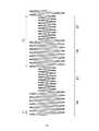
図2は、通信距離LE及び受信電圧VAの関係を示すグラフである。横軸は通信距離LEを示し、縦軸は受信電圧VAを示す。図1に示すように、アンテナ部103はアンテナ抵抗Ra及び開放電圧(受信電圧)VAで表される。開放電圧VAは、次式で表される。ここで、PAは受信電力である。抵抗Raは、例えば1kΩである。
VA=√(2×PA×Ra)FIG. 2 is a graph showing the relationship between the communication distance LE and the reception voltage VA. The horizontal axis indicates the communication distance LE, and the vertical axis indicates the reception voltage VA. As shown in FIG. 1, the
VA = √ (2 × PA × Ra)
すなわち、開放電圧VAは、通信距離LEに反比例する。このような特性があるため、開放電圧VAに準じた電流を抽出する信号抽出回路306(図3)を用いることにより、距離情報を持つ電流が抽出できる。タグ102は、この電流をアナログ形式からデジタル形式に変換し、リーダライタ101に距離情報を持つ電流の大きさを送信することができる。リーダライタ101は、電流の大きさを受信し、それを基に距離情報に変換することができる。 That is, the open circuit voltage VA is inversely proportional to the communication distance LE. Because of such characteristics, a current having distance information can be extracted by using the signal extraction circuit 306 (FIG. 3) that extracts a current in accordance with the open circuit voltage VA. The
タグ102は、リーダライタ101から受信した信号の大きさを検出する。その信号の大きさは、電流の大きさでも電圧の大きさでもよく、図2の関係を基に距離情報に変換される。その変換は、リーダライタ101で行ってもよいし、タグ102で行ってもよい。すなわち、タグ102は、信号の大きさを距離情報に変換し、その変換した距離情報をリーダライタ101に送信してもよい。 The
図3は、図1のタグ102の構成例を示す図である。タグ102は、リーダライタ101(図1)から照射される高周波信号から直流電源を得るとともに、同じ高周波信号から信号データを抽出するため、アンテナ部103、変調回路301、整流回路302、充電容量Ca、シャントレギュレータ303、復調回路304、デジタル信号処理部305及び信号抽出回路(電流モニタ)306を有する。 FIG. 3 is a diagram illustrating a configuration example of the
アンテナ部103は、所定の信号データが重畳された高周波信号を受信し、アンテナコイルによりアンテナ誘起電圧VAを発生させる。高周波信号は、リーダライタ101(図1)によって生成され、信号データに応じてASK(Amplitude Shift Keying)変調などの振幅変調が施されている。そして、アンテナ部103の持つ所定の抵抗Raによって、整流回路302に入力電圧VBを発生させる。 The
整流回路302は、アンテナ部103によって受信された高周波信号を整流して電源信号成分を取り出す回路であり、アンテナ部103が発生させる整流回路302の入力電圧VBから整流後の電源電圧VDD1を生成する。整流回路302の回路構成は、特に限定されないが、その例を後に図4を参照しながら説明する。 The
充電容量Caは、電源電圧VDD1を充電する。シャントレギュレータ303は、電圧制御回路であって、整流回路302によって電源用として整流した後の電源電圧VDD1を一定に保つように常に電圧を監視し、短絡電流の制御を行う。すなわち、電圧が高い場合には短絡電流を増やすことで定電圧に保つように制御を行っている。これは、主としてリーダライタ101(図1)からの距離LEによる電源電圧の変動を安定化させるためのものであるが、同時に搬送波に信号データが振幅変調されて振幅が変動する場合でも電圧を安定化させるよう作用する。 The charging capacity Ca charges the power supply voltage VDD1. The
信号抽出回路(電流モニタ)306は、整流回路12に流れる電流を検出(モニタ)し、電流値に応じた抽出信号A1を生成し、復調回路304へ出力する。整流回路302では、受信された高周波信号を整流しているが、高周波信号は信号データに応じて振幅変調されており、整流される電流もこれに伴って変動している。信号抽出回路(電流モニタ)306では、整流回路302に流れる電流の電流値を検出することにより、信号データを復調するための抽出信号を生成する。特に、シャントレギュレータ303によって短絡電流を消費して整流後の電源電圧変動を抑えている場合、受信した高周波信号に重畳されている信号データの“0”、“1”に応じた振幅の変化に応じてシャントレギュレータ303が短絡電流を制御することになる。このため、電源電圧が一定に保たれている状態であっても、整流回路302に流れる電流は、信号データに応じて変化する。すなわち、整流回路302に流れる電流の変化を検出することで、信号データを抽出することができる。 The signal extraction circuit (current monitor) 306 detects (monitors) the current flowing through the rectifier circuit 12, generates an
復調回路304は、信号抽出回路(電流モニタ)306から入力される抽出信号A1に基づき、信号データを復調し、デジタル信号を生成する。また、復調回路304は、信号A1の大きさをアナログ形式からデジタル形式に変換する。これらのデジタル信号は、デジタル信号処理部305で信号処理される。デジタル信号処理部305は、ID番号質問波を受信したときには自己のID番号を送信処理し、距離質問波を受信したときには受信電流A1の大きさを送信処理する。変調回路301は、デジタル信号処理部305から送られる送信信号に応じてアンテナ部103のインピーダンスに変調をかける。送信信号は、アンテナ部103からリーダライタ101に無線送信される。 The
図4は、図3の整流回路302及び信号抽出回路306の構成例を示す回路図である。整流回路302は、pチャネルMOS(Metal Oxide Semiconductor)電界効果トランジスタ401で構成される。トランジスタ401は、ゲート端子及びソース端子が相互に接続され、ダイオードを構成する。整流回路302は、半波整流を行う。信号抽出回路402は、pチャネルMOS電界効果トランジスタ402で構成される。トランジスタ401及び402は、相互にゲートが接続されるため、同じサイズであれば、同じドレイン電流A1が流れる。すなわち、電流A1は、整流回路401により整流された信号と同じ電流値になる。なお、トランジスタ402のサイズをトランジスタ401のサイズの1/100にすれば、トランジスタ402にはトランジスタ401の1/100の電流が流れる。信号抽出回路306は、電流A1を抽出して、復調回路304(図3)に出力する。 FIG. 4 is a circuit diagram showing a configuration example of the
整流回路302を構成するトランジスタ401は、ドレイン端子にアンテナ部103との接続点が接続され、ソース端子が充電容量Ca及び次段のシャントレギュレータ303に接続され、ゲート端子とソース端子が接続される。このトランジスタ401は、入力電圧VBの変化に応じてドレイン端子にかかる電圧がソース端子の電圧を超えたときドレイン−ソース間を電流が流れることによって、整流を行う。信号抽出回路306を構成するトランジスタ402は、ドレイン端子が整流回路302とアンテナ部103の接続点に接続され、ソース端子が復調回路304に接続され、ゲート端子が整流素子であるトランジスタ401のゲート端子と共通に接続される。この電流モニタ用のトランジスタ402は、入力電圧VBの変化に応じて整流回路302のトランジスタ401に電流が流れるとき、ドレイン電流A1が流れる。このように、トランジスタ402は、トランジスタ401に電流が流れるとき、その電流値に応じた抽出電流信号A1を生成することができる。 The
このような構成の整流回路302及び信号抽出回路306を有するタグ102の動作について説明する。信号データの“0”、“1”に応じて振幅変調された高周波信号がアンテナ部103より受信され、信号データ“0”の場合のアンテナ誘起電圧VA1もしくは信号データ“1”の場合のアンテナ誘起電圧VA2に応じた入力電圧VB1もしくはVB2が整流回路302に入力される。整流回路302は、入力信号から電源信号成分を取り出し、電源電圧VDD1を発生させる。シャントレギュレータ303は、電源電圧VDD1を監視し、電源電圧VDD1が一定となるように短絡電流を制御する。すなわち、整流回路302の入力電圧VB1、もしくは入力電圧VB2に応じて変化する整流回路302の出力電圧を短絡電流の制御によって一定に保つ。信号抽出回路306は、この電流変化を抽出信号として検出し、復調回路304へ出力する。なお、信号抽出回路306の抽出する電流信号A1は、整流回路302を構成する整流素子のオン抵抗に依存しない。 The operation of the
図6は、開放電圧(受信電圧)VAの波形例を示す図である。開放電圧VAは、周期T2の信号データが周期T1の搬送波で変調されている。例えば、周期T1は1ns、周期T2は25μsである。信号データは、“0”又は“1”のデジタル信号である。ピーク部PKは例えば信号データ“1”を示し、ボトム部BTは信号データ“0”を示す。 FIG. 6 is a diagram illustrating a waveform example of the open circuit voltage (reception voltage) VA. In the open circuit voltage VA, the signal data of the cycle T2 is modulated by the carrier wave of the cycle T1. For example, the period T1 is 1 ns, and the period T2 is 25 μs. The signal data is a digital signal of “0” or “1”. The peak portion PK indicates, for example, signal data “1”, and the bottom portion BT indicates signal data “0”.
図2において、開放電圧VAが6Vであれば、通信距離LEが1mであると判定することができる。容量Caに蓄積される電源電圧VDD1は、例えば3Vである。整流回路302の電圧降下は、例えば0.3Vである。抵抗Raは、例えば1kΩである。その場合、電圧VBが3.3V(=3+0.3)を超えたときのみ、電流A1が流れる。すなわち、電流A1は、開放電圧VAが3.3Vを超えた信号波形に対応する。開放電圧VAが6Vの時、抵抗Raを流れる電流A1は、次式で表される。
A1=(6V−3.3V)/1kΩ=2.7mAIn FIG. 2, if the open circuit voltage VA is 6V, it can be determined that the communication distance LE is 1 m. The power supply voltage VDD1 stored in the capacitor Ca is 3V, for example. The voltage drop of the
A1 = (6V-3.3V) / 1 kΩ = 2.7 mA
図5は、図1の復調回路304の構成例を示す図である。ピーク検出回路501は、電流信号A1のピーク部PK(図6)を検出する。ボトム検出回路502は、電流信号A1のボトム部BT(図6)を検出する。中間レベル検出回路503は、ピーク検出回路501で検出されたピーク部PKの電流値A2とボトム部502で検出されたボトム部BTの電流値A3との中間値(平均値)A4を検出する。コンパレータ504は、電流信号A1及び中間値A4を比較し、比較結果をデジタルデータ信号A5としてデジタル信号処理部305に出力する。例えば、電流信号A1が中間信号A4より大きければデータ信号A5として“1”を出力し、電流信号A1が中間信号A4より小さければデータ信号A5として“0”を出力する。A(アナログ)/D(デジタル)変換回路505は、デジタル信号処理部305からスタート信号STを入力すると、ピーク部PKの電流値A2をアナログ形式からデジタル形式に変換し、デジタル信号A6をデジタル信号処理部305に出力する。 FIG. 5 is a diagram illustrating a configuration example of the
上記のように、ピーク部PKを検出してピーク電流値A2をデジタル信号に変換することにより、データ内容に依存しない受信信号(電流)の大きさを測定することができる。これにより、正確な距離情報を得ることができる。なお、A/D変換回路505において、ピーク電流値A2の代わりに、ボトム電流値A3をアナログ形式からデジタル形式に変換してもよい。 As described above, by detecting the peak portion PK and converting the peak current value A2 into a digital signal, the magnitude of the received signal (current) independent of the data content can be measured. Thereby, accurate distance information can be obtained. In the A /
図7は、図3のデジタル信号処理部305の構成例を示す図である。ロジック回路701は、復調回路304からデータ信号A5を入力し、そのデータ信号A5のコマンドに応じた処理を行う。そのコマンド内でID番号が指定されているときには、そのID番号と自己のID番号が同じときのみ、ロジック回路701は処理を行う。 FIG. 7 is a diagram illustrating a configuration example of the digital
ロジック回路701は、リーダライタ101からID番号質問波を受信したときには、メモリ704内の自己のID番号を読み出し、送信回路705に送信指示する。送信回路705は、そのID番号を送信信号A7として出力する。 When the
デジタル信号処理部305は、受信信号の大きさを示す信号A6をそのままリーダライタ101に送信する場合には変換回路702が不要である。パラレル/シリアル変換回路703は、例えば7ビットの信号A6をパラレルからシリアルに変換し、送信回路705に出力する。ロジック回路701は、リーダライタ101から距離質問波を受信したときには、信号A6を送信するように送信回路705に指示する。送信回路705は、信号A6のシリアル信号をID番号と共に送信信号A7として出力する。 The digital
次に、変換回路702を設ける場合を説明する。変換回路702は、図2のグラフと同様に、電流A6から通信距離LEに変換するためのテーブル又は変換式を有し、電流A6から通信距離LEへの変換を行う。パラレル/シリアル変換回路703は、その通信距離LEの信号をパラレルからシリアルに変換し、送信回路705に出力する。ロジック回路701は、リーダライタ101から距離質問波を受信したときには、通信距離LEを送信するように送信回路705に指示する。送信回路705は、通信距離LEのシリアル信号をID番号と共に送信信号A7として出力する。 Next, the case where the
送信信号A7は、変調回路301により変調され、アンテナ部103からリーダライタ101に無線送信される。 The transmission signal A7 is modulated by the
また、ロジック回路701は、距離質問波(コマンド)を受信すると、A/D変換のスタート信号STをA/D変換回路505に出力する。A/D変換回路505は、スタート信号STが入力されると、アナログ形式からデジタル形式への変換を開始する。 When the
また、A/D変換回路505は、スタート信号STにかかわらずにアナログ形式からデジタル形式への変換を行ってもよい。そのデジタル信号又は距離情報は、復調回路305内に記憶される。ロジック回路701は、距離質問波(コマンド)を受信すると、その記憶されている上記のデジタル信号又は距離情報を送信処理することができる。 In addition, the A /
図8は、図5のA/D変換回路505の構成例を示す回路図である。A/D変換回路505は、フラッシュ型A/D変換器801、A/Dインターフェース802、エンコーダ803、レジスタ804及びコントローラ805を有する。 FIG. 8 is a circuit diagram showing a configuration example of the A /
コントローラ805は、それぞれ、制御信号VDIV2、VDIV4、VDIV8、VDIV16、VDIV32及びVMUL2を介して、セレクタ821〜826を制御する。除算器811は、受信電流A2を1/2にして出力する。セレクタ821は、制御信号VDIV2に応じて、受信電流A2又は除算器811の出力信号を選択して出力する。除算器812は、セレクタ821の出力信号を1/2にして出力する。セレクタ822は、制御信号VDIV4に応じて、セレクタ821の出力信号又は除算器812の出力信号を選択して出力する。除算器813は、セレクタ822の出力信号を1/2にして出力する。セレクタ823は、制御信号VDIV8に応じて、セレクタ822の出力信号又は除算器813の出力信号を選択して出力する。除算器814は、セレクタ823の出力信号を1/2にして出力する。セレクタ824は、制御信号VDIV16に応じて、セレクタ823の出力信号又は除算器814の出力信号を選択して出力する。除算器815は、セレクタ824の出力信号を1/2にして出力する。セレクタ825は、制御信号VDIV32に応じて、セレクタ824の出力信号又は除算器815の出力信号を選択して出力する。乗算器816は、セレクタ825の出力信号を2倍にして出力する。セレクタ826は、制御信号VMUL2に応じて、セレクタ825の出力信号又は乗算器816の出力信号を選択して出力する。スイッチ827は、制御信号VTに応じて、セレクタ826の出力信号を演算器831〜838に出力する。 The
演算器831〜838は、セレクタ826の出力信号を、それぞれ1倍、15/16倍、14/16倍、13/16倍、12/16倍、11/16倍、10/16倍、9/16倍して出力する。コンパレータ841〜848は、それぞれ演算器831〜838の出力信号と基準電流IBとを比較し、比較結果をA/Dインターフェース802を介してエンコーダ803に出力する。 The
エンコーダ803は、コンパレータ841〜848の比較結果をエンコードし、下位4ビットのデジタル信号VYを出力する。コントローラ805は、セレクタ821〜826の選択状態に応じて、レジスタ804に上位3ビットのデジタル信号VEを出力する。7ビットのデジタル信号A6は、上位3ビット信号VE及び下位4ビット信号VYからなり、A/D変換回路505の出力信号となる。 The
セレクタ821〜826は、受信電流A2を2倍〜1/32倍の大きさにすることができる。上位3ビット信号VEは、その倍率に対応する。コンパレータ841〜848は、さらに、その信号を1倍〜9/16倍した信号と基準電流IBとの比較を行い、1/16精度の比較を行う。その比較結果が、下位4ビット信号VYに対応する。コントローラ805は、コンパレータ841の出力信号に対応する信号VDOWN及びコンパレータ848の出力信号に対応する信号VUPに応じて、制御を行う。以上の構成により、A/D変換回路505は、アナログ信号A2をデジタル信号A6に変換することができる。 The
以上のように、A/D変換回路505は、演算器811〜816及びセレクタ821〜826により、受信した信号値を2M倍又は2M分の1(Mは自然数)にし、それを基に基準信号値IBと比較することにより、その受信した信号値をアナログ形式からデジタル形式に変換する。 As described above, the A /
また、A/D変換回路505は、演算器831〜838により、その2M倍又は2M分の1にされた信号値をN/P倍(N及びPは自然数)し、それを基準信号値IBと比較することにより、その受信した信号値をアナログ形式からデジタル形式に変換する。 Further, the A /
図9は、図8の基準電流IBを生成するための回路の構成例を示す回路図である。基準電圧発生回路(BGR)901は、基準電圧V1を生成する。コンパレータ902は、電圧V1及びV2を比較し、その比較結果をpチャネルMOS電界効果トランジスタ905のゲートに出力する。電圧V2は、トランジスタ905のドレイン電圧である。トランジスタ905のドレインは、抵抗904を介してグランドに接続される。トランジスタ905のソースは電源電圧に接続される。pチャネルMOS電界効果トランジスタ906は、ゲートがトランジスタ905のゲートに接続され、ソースが電源電圧に接続される。トランジスタ906のドレイン電流が基準電流IBとなる。 FIG. 9 is a circuit diagram showing a configuration example of a circuit for generating the reference current IB of FIG. A reference voltage generation circuit (BGR) 901 generates a reference voltage V1.
コンパレータ902及びトランジスタ905の働きにより、電圧V2は電圧V1と同じになる。電圧V1及びV2は、例えば1.2Vである。抵抗904は、例えば1.2MΩである。抵抗904を流れる電流IAは、1.2V/1.2MΩ=1μAである。トランジスタ905及び906は、カレントミラー回路を構成し、電流IA及びIBは同じになる。これにより、基準電流IBは、1μAの定電流となる。 The voltage V2 becomes the same as the voltage V1 by the operation of the
図10は、図1のリーダライタ101の構成例を示す図である。上記のタグ102が信号の大きさをリーダライタ101に送信する場合には、リーダライタ101は変換回路1006を必要とする。これに対し、上記のタグ102が距離情報をリーダライタ101に送信する場合には、リーダライタ101は変換回路1006が不要である。 FIG. 10 is a diagram illustrating a configuration example of the reader /
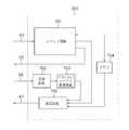
リーダライタ101は、タグ102に無線信号で電源を供給し、タグ102と無線通信を行うため、アンテナ部1001、共用器1002、増幅器1003、直交ミキサ1004、フィルタ1007、復調器1008、発振器1009、フィルタ1010、ASK変調器1011、増幅器1012、及び処理回路1005を有する。以下、動作を説明する。 The reader /
リーダライタ101はLAN1013とで情報信号の受信又はタイミング情報の送信を処理回路1005を介して行なう。処理回路1005は自身で生成したコマンドおよびLAN1013から受信した情報信号をフィルタ1010へ出力する。フィルタ1010はプロセッサ1005からのデータの帯域を制限した信号としてASK変調器1011へ出力する。ASK変調器1011は発振器1009からの搬送信号をフィルタ1010からの信号にてASK(振幅変調)される。また、ASK信号は増幅器1012で増幅され、共用器1002、アンテナ1001を介してRFタグに向けて送信する。 The reader /
次に、リーダーにおけるRFタグからの信号(アンテナの反射率を変えて変調した信号のことを示す)の受信動作については、図10を用いて以下のとおり説明する。 Next, the reception operation of the signal from the RF tag in the reader (which indicates a signal modulated by changing the reflectance of the antenna) will be described as follows with reference to FIG.
アンテナ1001は受信した信号(以下、変調信号と称す。)を、共用器1002を介し、増幅器1003で増幅して直交ミキサ1004に出力する。直交ミキサ1004は増幅された変調信号を発振器1009の出力によりIF信号に復調する。フィルタ1007はLPFで、高周波成分を除去することで、IF信号の隣接チャンネル間干渉を抑えるのに使用している。 The
復調器1008はフィルタ1007からの信号をデータに復調して、プロセッサ1005へ出力する。プロセッサ1005は復調されたデータを処理する、またはプロセッサ1005はLAN1013にタグから読み込んだデータ等を出力する。 The
まず、リーダライタ101がタグ102から距離情報を受信した場合を説明する。その場合、処理回路1005は、復調された信号を基に直ちに距離情報を得ることができる。 First, a case where the reader /
次に、リーダライタ101がタグ102から信号の大きさを受信した場合を説明する。処理回路1005内の変換回路1006は、図7の変換回路702と同様であり、復調された信号の大きさを距離情報に変換する。これにより、処理回路1005は、距離情報を得ることができる。 Next, a case where the reader /
また、信号の大きさをそのままLANへ出力し、LANに接続された別のシステム201内に変換回路2001があり、これが図7の変換回路と同様であり、復調された信号の大きさを距離情報に変換する場合もある。 Further, the signal size is output to the LAN as it is, and there is a
以上のように、リーダライタ101は、アンテナを介して信号をタグ102へ送信する。次に、タグ102は、リーダライタ101からアンテナを介して受信した信号の大きさをアナログ形式からデジタル形式に変換し、そのデジタル形式の信号又はそれを基にした信号をアンテナを介してリーダライタ101へ送信する。次に、リーダライタ101は、その送信された信号をアンテナを介してタグ102から受信して距離情報を得る。リーダライタ101が上記のデジタル形式の信号を受信したときには、その受信した信号を基に距離情報に変換する。 As described above, the reader /
少なくとも1個の移動可能なタグ102に対して2次元又は3次元に固定された複数のリーダライタ101を設ければ、複数のリーダライタ101とタグ102との間のそれぞれの距離を測定することができる。これにより、リーダライタ101は、タグ102の2次元座標又は3次元座標の位置を演算して求めることができる。 If a plurality of reader /
また、少なくとも1個の移動可能なリーダライタ101に対して2次元又は3次元に固定された複数のタグ102を設ければ、複数のタグ102とリーダライタ101との間のそれぞれの距離を測定することができる。これにより、リーダライタ101は、リーダライタ101の2次元座標又は3次元座標の位置を演算して求めることができる。 Further, if a plurality of
本実施形態は、上記の特許文献1に比べ、複数のアンテナを使用せず、到達距離が段階的に異なる質問波を順に発することもないので、コストを低減することができる。また、複数回の異なる質問波でアクセスするのではないので、高速に距離を測定することが可能になる。また、本実施形態は、上記の特許文献2のようにリーダライタがタグからの戻りの無線信号の時間、強度又は波形形状を検出してタグの距離を決定するシステムに比べ、信号のばらつきが小さく、信号の電力が大きいので、雑音耐力が高く、距離を正確に測定することができる。 Compared with
また、本実施形態は、上記の特許文献2のようにリーダライタがタグで反射した戻り信号を測定する場合に比べ、タグの反射係数のバラツキに依存しない。また、本実施形態のタグが受信する電力は、特許文献2の反射してさらに減衰した後にリーダライタに届く信号に比べ、はるかに大きいため、雑音耐力が高い。 Further, the present embodiment does not depend on variations in the reflection coefficient of the tag as compared to the case where the reader / writer measures the return signal reflected by the tag as in
なお、上記実施形態は、何れも本発明を実施するにあたっての具体化の例を示したものに過ぎず、これらによって本発明の技術的範囲が限定的に解釈されてはならないものである。すなわち、本発明はその技術思想、またはその主要な特徴から逸脱することなく、様々な形で実施することができる。 The above-described embodiments are merely examples of implementation in carrying out the present invention, and the technical scope of the present invention should not be construed in a limited manner. That is, the present invention can be implemented in various forms without departing from the technical idea or the main features thereof.
本発明の実施形態は、例えば以下のように種々の適用が可能である。 The embodiment of the present invention can be applied in various ways as follows, for example.
(付記1)
アンテナを介して受信した信号の大きさをアナログ形式からデジタル形式に変換するアナログ/デジタル変換回路と、
前記デジタル形式の信号又はそれを基にした信号をアンテナを介して送信する送信回路と
を有することを特徴とするRFIDタグ装置。
(付記2)
さらに、前記受信した信号を整流する整流回路を有し、
前記アナログ/デジタル変換回路は、前記整流された信号の大きさをアナログ形式からデジタル形式に変換することを特徴とする付記1記載のRFIDタグ装置。
(付記3)
さらに、前記整流された信号を基に電源電圧を充電するための容量を有することを特徴とする付記2記載のRFIDタグ装置。
(付記4)
さらに、前記容量に充電される電源電圧を一定に保つために短絡電流量を制御するシャントレギュレータを有することを特徴とする付記3記載のRFIDタグ装置。
(付記5)
前記アナログ/デジタル変換回路は、前記受信した信号の電流値をアナログ形式からデジタル形式に変換することを特徴とする付記1記載のRFIDタグ装置。
(付記6)
さらに、前記受信した信号の電流をモニタするためのモニタ回路を有し、
前記アナログ/デジタル変換回路は、前記モニタされた電流値をアナログ形式からデジタル形式に変換することを特徴とする付記5記載のRFIDタグ装置。
(付記7)
さらに、前記受信した信号のピーク部を検出するためのピーク検出回路を有し、
前記アナログ/デジタル変換回路は、前記検出されたピーク部の信号をアナログ形式からデジタル形式に変換することを特徴とする付記1記載のRFIDタグ装置。
(付記8)
さらに、前記受信した信号のボトム部を検出するためのボトム検出回路を有し、
前記アナログ/デジタル変換回路は、前記検出されたボトム部の信号をアナログ形式からデジタル形式に変換することを特徴とする付記1記載のRFIDタグ装置。
(付記9)
前記アナログ/デジタル変換回路は、特定のコマンドを受信したときに、アナログ形式からデジタル形式への変換を開始することを特徴とする付記1記載のRFIDタグ装置。
(付記10)
前記送信回路は、特定のコマンドを受信したときに、前記信号を送信することを特徴とする付記1記載のRFIDタグ装置。
(付記11)
前記アナログ/デジタル変換回路は、前記受信した信号値を2M倍又は2M分の1(Mは自然数)にし、それを基に基準信号値と比較することにより、前記受信した信号値をアナログ形式からデジタル形式に変換することを特徴とする付記1記載のRFIDタグ装置。
(付記12)
前記アナログ/デジタル変換回路は、前記2M倍又は2M分の1にされた信号値をN/P倍(N及びPは自然数)し、それを基準信号値と比較することにより、前記受信した信号値をアナログ形式からデジタル形式に変換することを特徴とする付記11記載のRFIDタグ装置。
(付記13)
前記送信回路は、前記デジタル形式の信号を距離情報に変換し、その距離情報をアンテナを介して送信することを特徴とする付記1記載のRFIDタグ装置。
(付記14)
前記アナログ/デジタル変換回路は、前記受信した信号の電流値をアナログ形式からデジタル形式に変換することを特徴とする付記4記載のRFIDタグ装置。
(付記15)
さらに、前記整流された信号の電流をモニタするためのモニタ回路を有し、
前記アナログ/デジタル変換回路は、前記モニタされた電流値をアナログ形式からデジタル形式に変換することを特徴とする付記14記載のRFIDタグ装置。
(付記16)
さらに、前記モニタされた電流のピーク部を検出するためのピーク検出回路を有し、
前記アナログ/デジタル変換回路は、前記検出されたピーク部の電流値をアナログ形式からデジタル形式に変換することを特徴とする付記15記載のRFIDタグ装置。
(付記17)
さらに、前記モニタされた電流のボトム部を検出するためのボトム検出回路を有し、
前記アナログ/デジタル変換回路は、前記検出されたボトム部の電流値をアナログ形式からデジタル形式に変換することを特徴とする付記15記載のRFIDタグ装置。
(付記18)
アンテナを介して信号を送信する送信回路と、
前記送信した信号の大きさを示す信号をアンテナを介して受信し、その受信した信号を基に距離情報に変換する変換回路と
を有することを特徴とするRFIDリーダライタ装置。
(付記19)
RFIDリーダライタ装置及びRFIDタグ装置を有する距離測定システムであって、
前記RFIDリーダライタ装置は、
アンテナを介して信号を前記RFIDタグ装置へ送信する第1の送信回路と、
前記送信後に信号をアンテナを介して前記RFIDタグ装置から受信して距離情報を得る処理回路とを有し、
前記RFIDタグ装置は、
前記RFIDリーダライタ装置からアンテナを介して受信した信号の大きさをアナログ形式からデジタル形式に変換するアナログ/デジタル変換回路と、
前記デジタル形式の信号又はそれを基にした信号をアンテナを介して前記RFIDリーダライタ装置へ送信する第2の送信回路とを有することを特徴とする距離測定システム。
(付記20)
前記処理回路は、前記受信した信号を基に距離情報に変換することを特徴とする付記19記載の距離測定システム。(Appendix 1)
An analog / digital conversion circuit for converting the magnitude of a signal received via an antenna from an analog format to a digital format;
An RFID tag device comprising: a transmission circuit that transmits the digital signal or a signal based on the digital signal via an antenna.
(Appendix 2)
And a rectifier circuit for rectifying the received signal,
The RFID tag device according to
(Appendix 3)
The RFID tag device according to
(Appendix 4)
The RFID tag device according to
(Appendix 5)
The RFID tag device according to
(Appendix 6)
And a monitor circuit for monitoring the current of the received signal,
The RFID tag device according to appendix 5, wherein the analog / digital conversion circuit converts the monitored current value from an analog format to a digital format.
(Appendix 7)
Furthermore, it has a peak detection circuit for detecting a peak portion of the received signal,
The RFID tag device according to
(Appendix 8)
Furthermore, it has a bottom detection circuit for detecting the bottom portion of the received signal,
The RFID tag device according to
(Appendix 9)
The RFID tag device according to
(Appendix 10)
The RFID tag device according to
(Appendix 11)
The analog / digital conversion circuit multiplies the received signal value by 2M or 1 / 2M (M is a natural number), and compares the received signal value with an analog format by comparing it with a reference signal value. The RFID tag device according to
(Appendix 12)
The analog / digital conversion circuit multiplies the signal value that has been multiplied by 2M or 2M by N / P (N and P are natural numbers) and compares it with a reference signal value, thereby receiving the received signal. The RFID tag device according to
(Appendix 13)
The RFID tag device according to
(Appendix 14)
The RFID tag device according to appendix 4, wherein the analog / digital conversion circuit converts the current value of the received signal from an analog format to a digital format.
(Appendix 15)
And a monitor circuit for monitoring a current of the rectified signal,
15. The RFID tag device according to appendix 14, wherein the analog / digital conversion circuit converts the monitored current value from an analog format to a digital format.
(Appendix 16)
And a peak detection circuit for detecting a peak portion of the monitored current,
The RFID tag device according to appendix 15, wherein the analog / digital conversion circuit converts the detected current value of the peak portion from an analog format to a digital format.
(Appendix 17)
And a bottom detection circuit for detecting a bottom portion of the monitored current,
16. The RFID tag device according to appendix 15, wherein the analog / digital conversion circuit converts the detected current value of the bottom portion from an analog format to a digital format.
(Appendix 18)
A transmission circuit for transmitting a signal via an antenna;
An RFID reader / writer device comprising: a conversion circuit that receives a signal indicating the magnitude of the transmitted signal through an antenna and converts the signal into distance information based on the received signal.
(Appendix 19)
A distance measuring system having an RFID reader / writer device and an RFID tag device,
The RFID reader / writer device is
A first transmission circuit for transmitting a signal to the RFID tag device via an antenna;
A processing circuit for obtaining distance information by receiving a signal from the RFID tag device via an antenna after the transmission;
The RFID tag device is
An analog / digital conversion circuit for converting the magnitude of a signal received from the RFID reader / writer device via an antenna from an analog format to a digital format;
And a second transmission circuit for transmitting the digital signal or a signal based on the signal to the RFID reader / writer device via an antenna.
(Appendix 20)
20. The distance measuring system according to appendix 19, wherein the processing circuit converts distance information based on the received signal.
101 リーダライタ
102 タグ
103 アンテナ部
104 タグIC
301 変調回路
302 整流回路
303 シャントレギュレータ
304 復調回路
305 デジタル信号処理部
306 信号抽出回路101 Reader /
301
Claims (10)
Translated fromJapanese前記デジタル形式の信号又はそれを基にした信号をアンテナを介して送信する送信回路と
を有することを特徴とするRFIDタグ装置。An analog / digital conversion circuit for converting the magnitude of a signal received via an antenna from an analog format to a digital format;
An RFID tag device comprising: a transmission circuit that transmits the digital signal or a signal based on the digital signal via an antenna.
前記アナログ/デジタル変換回路は、前記検出されたピーク部の信号をアナログ形式からデジタル形式に変換することを特徴とする請求項1記載のRFIDタグ装置。Furthermore, it has a peak detection circuit for detecting a peak portion of the received signal,
2. The RFID tag device according to claim 1, wherein the analog / digital conversion circuit converts the detected peak signal from an analog format to a digital format.
前記アナログ/デジタル変換回路は、前記検出されたボトム部の信号をアナログ形式からデジタル形式に変換することを特徴とする請求項1記載のRFIDタグ装置。Furthermore, it has a bottom detection circuit for detecting the bottom portion of the received signal,
2. The RFID tag device according to claim 1, wherein the analog / digital conversion circuit converts the detected bottom signal from an analog format to a digital format.
前記送信した信号の大きさを示す信号をアンテナを介して受信し、その受信した信号を基に距離情報に変換する変換回路と
を有することを特徴とするRFIDリーダライタ装置。A transmission circuit for transmitting a signal via an antenna;
An RFID reader / writer device comprising: a conversion circuit that receives a signal indicating the magnitude of the transmitted signal through an antenna and converts the signal into distance information based on the received signal.
前記RFIDリーダライタ装置は、
アンテナを介して信号を前記RFIDタグ装置へ送信する第1の送信回路と、
前記送信後に信号をアンテナを介して前記RFIDタグ装置から受信して距離情報を得る処理回路とを有し、
前記RFIDタグ装置は、
前記RFIDリーダライタ装置からアンテナを介して受信した信号の大きさをアナログ形式からデジタル形式に変換するアナログ/デジタル変換回路と、
前記デジタル形式の信号又はそれを基にした信号をアンテナを介して前記RFIDリーダライタ装置へ送信する第2の送信回路とを有することを特徴とする距離測定システム。A distance measuring system having an RFID reader / writer device and an RFID tag device,
The RFID reader / writer device is
A first transmission circuit for transmitting a signal to the RFID tag device via an antenna;
A processing circuit for obtaining distance information by receiving a signal from the RFID tag device via an antenna after the transmission;
The RFID tag device is
An analog / digital conversion circuit for converting the magnitude of a signal received from the RFID reader / writer device via an antenna from an analog format to a digital format;
And a second transmission circuit for transmitting the digital signal or a signal based on the signal to the RFID reader / writer device via an antenna.
Priority Applications (6)
| Application Number | Priority Date | Filing Date | Title |
|---|---|---|---|
| JP2005250158AJP2007064765A (en) | 2005-08-30 | 2005-08-30 | RFID tag device, RFID reader / writer device, and distance measurement system |
| TW095106347ATW200708755A (en) | 2005-08-30 | 2006-02-24 | RFID tag device, RFID reader/writer device, and distance measuring system |
| KR1020060018991AKR100765877B1 (en) | 2005-08-30 | 2006-02-27 | Rfid tag device, rfid reader/writer device, and distance measuring system |
| US11/362,097US20070046430A1 (en) | 2005-08-30 | 2006-02-27 | RFID tag device, RFID reader/writer device, and distance measuring system |
| EP06251132AEP1760640A1 (en) | 2005-08-30 | 2006-03-02 | System for measuring the distance between an RFID tag and a base station |
| CNA2006100654491ACN1924609A (en) | 2005-08-30 | 2006-03-22 | RFID tag device, RFID reader/writer device, and distance measuring system |
Applications Claiming Priority (1)
| Application Number | Priority Date | Filing Date | Title |
|---|---|---|---|
| JP2005250158AJP2007064765A (en) | 2005-08-30 | 2005-08-30 | RFID tag device, RFID reader / writer device, and distance measurement system |
Publications (1)
| Publication Number | Publication Date |
|---|---|
| JP2007064765Atrue JP2007064765A (en) | 2007-03-15 |
Family
ID=37103062
Family Applications (1)
| Application Number | Title | Priority Date | Filing Date |
|---|---|---|---|
| JP2005250158APendingJP2007064765A (en) | 2005-08-30 | 2005-08-30 | RFID tag device, RFID reader / writer device, and distance measurement system |
Country Status (6)
| Country | Link |
|---|---|
| US (1) | US20070046430A1 (en) |
| EP (1) | EP1760640A1 (en) |
| JP (1) | JP2007064765A (en) |
| KR (1) | KR100765877B1 (en) |
| CN (1) | CN1924609A (en) |
| TW (1) | TW200708755A (en) |
Cited By (7)
| Publication number | Priority date | Publication date | Assignee | Title |
|---|---|---|---|---|
| KR100789170B1 (en) | 2007-03-27 | 2008-01-02 | 이향제 | Car proximity sensor using passive RFID |
| KR100799853B1 (en) | 2007-04-16 | 2008-02-01 | 이향제 | Car proximity sensor using passive RFID |
| KR100865335B1 (en) | 2007-06-29 | 2008-10-27 | 한국과학기술원 | Digital Signal Restoration Circuit and Digital Signal Restoration Method |
| JP2016121932A (en)* | 2014-12-25 | 2016-07-07 | 大日本印刷株式会社 | Paper residual quantity measurement system and paper residual quantity measurement device |
| JP2017080809A (en)* | 2015-10-29 | 2017-05-18 | リンカーン グローバル,インコーポレイテッド | System and method for communicating over a welding power cable in a welding system |
| JP2024075609A (en)* | 2016-05-13 | 2024-06-04 | グーグル エルエルシー | SYSTEMS, METHODS AND DEVICES FOR UTILIZING RADAR IN SMART DEVICES - Patent application |
| US12262289B2 (en) | 2016-05-13 | 2025-03-25 | Google Llc | Systems, methods, and devices for utilizing radar with smart devices |
Families Citing this family (43)
| Publication number | Priority date | Publication date | Assignee | Title |
|---|---|---|---|---|
| US7510117B2 (en)* | 2004-06-04 | 2009-03-31 | Impinj Inc | Decoding with memory in RFID system |
| US9542577B2 (en) | 2005-12-09 | 2017-01-10 | Tego, Inc. | Information RFID tagging facilities |
| US8988223B2 (en) | 2005-12-09 | 2015-03-24 | Tego Inc. | RFID drive management facility |
| EP1958172B1 (en) | 2005-12-09 | 2014-11-12 | Tego Inc. | Multiple radio frequency network node rfid tag |
| US8242908B2 (en) | 2005-12-09 | 2012-08-14 | Tego Inc. | Methods and systems of a multiple radio frequency network node RFID tag |
| US8279065B2 (en) | 2005-12-09 | 2012-10-02 | Tego Inc. | Methods and systems of a multiple radio frequency network node RFID tag |
| US9117128B2 (en) | 2005-12-09 | 2015-08-25 | Tego, Inc. | External access to memory on an RFID tag |
| US8242911B2 (en) | 2006-12-11 | 2012-08-14 | Tego Inc. | Composite multiple RFID tag facility |
| US9418263B2 (en) | 2005-12-09 | 2016-08-16 | Tego, Inc. | Operating systems for an RFID tag |
| US9430732B2 (en) | 2014-05-08 | 2016-08-30 | Tego, Inc. | Three-dimension RFID tag with opening through structure |
| US8269630B2 (en) | 2005-12-09 | 2012-09-18 | Tego Inc. | Methods and systems of a multiple radio frequency network node RFID tag |
| US8947233B2 (en) | 2005-12-09 | 2015-02-03 | Tego Inc. | Methods and systems of a multiple radio frequency network node RFID tag |
| US8390456B2 (en) | 2008-12-03 | 2013-03-05 | Tego Inc. | RFID tag facility with access to external devices |
| US9361568B2 (en) | 2005-12-09 | 2016-06-07 | Tego, Inc. | Radio frequency identification tag with hardened memory system |
| JP4787945B2 (en)* | 2006-07-14 | 2011-10-05 | ソニー・エリクソン・モバイルコミュニケーションズ株式会社 | Non-contact communication circuit and portable terminal |
| JP5179858B2 (en)* | 2007-01-06 | 2013-04-10 | 株式会社半導体エネルギー研究所 | Semiconductor device |
| FR2915801B1 (en) | 2007-05-03 | 2009-07-17 | Taema Sa | METHOD FOR CONTROLLING A HOMOGENEOUS BATCH OF FLUID BOTTLES UNDER PRESSURE |
| FR2915799B1 (en) | 2007-05-03 | 2010-10-01 | Taema | ELECTRONIC PRESSURE MEASURING PRESSURE GAUGE IN A CONTAINER |
| FR2915821B1 (en)* | 2007-05-03 | 2009-11-20 | Air Liquide | METHOD FOR PROCESSING DATA RELATING TO A PRESSURIZED FLUID BOTTLE |
| FR2915798B1 (en) | 2007-05-03 | 2010-04-30 | Taema | METHOD FOR CONTROLLING AN ELECTRONIC MANOMETER AND CORRESPONDING MANOMETER |
| US8292175B2 (en) | 2007-06-08 | 2012-10-23 | Lg Innotek Co., Ltd. | Tag device, reader device, and RFID system |
| KR100911821B1 (en)* | 2007-07-16 | 2009-08-12 | 엘지이노텍 주식회사 | RFID tag |
| JP5350389B2 (en)* | 2007-10-28 | 2013-11-27 | テゴ,インコーポレイテッド | Method and system for sharing power in a multiple radio frequency network node RFID tag |
| DE102007060571A1 (en) | 2007-12-15 | 2009-06-18 | Polyic Gmbh & Co. Kg | Reader, to read data stored in an organic transponder, transmits a reference signal for the response to set the transmission power to read the data without transponder damage |
| JP2009222590A (en)* | 2008-03-17 | 2009-10-01 | Fujitsu Ltd | Testing device and testing method |
| US20090262012A1 (en)* | 2008-04-16 | 2009-10-22 | Paul Carlson | Radiometer and temperature compensation system |
| US8632002B2 (en)* | 2008-07-08 | 2014-01-21 | International Business Machines Corporation | Real-time security verification for banking cards |
| US8615465B2 (en)* | 2008-07-08 | 2013-12-24 | International Business Machines Corporation | Real-time security verification for banking cards |
| US8638255B2 (en)* | 2008-07-30 | 2014-01-28 | Nxp B.V. | System for reading information transmitted from a transponder |
| US8299652B2 (en) | 2008-08-20 | 2012-10-30 | Intel Corporation | Wireless power transfer apparatus and method thereof |
| US20100081379A1 (en)* | 2008-08-20 | 2010-04-01 | Intel Corporation | Wirelessly powered speaker |
| CN101770009B (en)* | 2009-01-06 | 2014-05-21 | 成都西谷曙光数字技术有限公司 | New accurate and practical radio-frequency positioning technology |
| US8068012B2 (en)* | 2009-01-08 | 2011-11-29 | Intelleflex Corporation | RFID device and system for setting a level on an electronic device |
| EP2239374B2 (en)† | 2009-04-03 | 2017-03-15 | Joseph Vögele AG | Paver |
| DE102011054926A1 (en)* | 2011-10-28 | 2013-05-02 | Caterpillar Global Mining Europe Gmbh | Method and system for increasing the operational safety of mobile machines in surface mining or underground mines for the extraction of minerals using RFID technology |
| EP2808823B1 (en)* | 2012-02-27 | 2018-02-21 | Centro Nacional De Tecnologia Avançada - Ceitec S.A. | Data-detector circuit for rfid tags |
| US8824597B2 (en)* | 2012-09-07 | 2014-09-02 | Texas Instruments Incorporated | Circuits and methods for field-based communication |
| KR102089652B1 (en) | 2013-09-16 | 2020-03-16 | 삼성전자주식회사 | Near field communication devices, electronic systems having the same and method of controlling power in near field communication devices |
| KR102048016B1 (en) | 2013-12-30 | 2019-11-22 | 삼성전자주식회사 | NFC Terminal and Comunication Device including Thereof |
| US9953193B2 (en) | 2014-09-30 | 2018-04-24 | Tego, Inc. | Operating systems for an RFID tag |
| US20180018654A1 (en)* | 2016-07-15 | 2018-01-18 | Mike Miskin | Portable electronic payment security devices, systems and methods |
| US11886216B2 (en)* | 2021-11-02 | 2024-01-30 | Nxp B.V. | Voltage regulator circuit and method for regulating a voltage |
| CN118133869B (en)* | 2024-02-08 | 2025-04-04 | 支付宝(杭州)信息技术有限公司 | Communication devices, chips and equipment |
Family Cites Families (25)
| Publication number | Priority date | Publication date | Assignee | Title |
|---|---|---|---|---|
| DE4227551A1 (en)* | 1992-08-20 | 1994-02-24 | Eurosil Electronic Gmbh | Chip card with field strength detector |
| EP0650074A1 (en)* | 1993-10-22 | 1995-04-26 | Texas Instruments Holland B.V. | Highly accurate RF-ID positioning system |
| FR2746200B1 (en)* | 1996-03-12 | 1998-05-29 | NON-CONTACT INFORMATION EXCHANGE DEVICE WITH AN ELECTRONIC LABEL | |
| US6710701B2 (en)* | 1998-04-22 | 2004-03-23 | Gilbarco Inc. | Rfid tag location using tag or host interaction record |
| GB9821046D0 (en)* | 1998-09-28 | 1998-11-18 | Whitesmith Howard W | Detection system |
| US7558616B2 (en)* | 1999-03-11 | 2009-07-07 | Biosense, Inc. | Guidance of invasive medical procedures using implantable tags |
| US7590441B2 (en)* | 1999-03-11 | 2009-09-15 | Biosense, Inc. | Invasive medical device with position sensing and display |
| US7174201B2 (en)* | 1999-03-11 | 2007-02-06 | Biosense, Inc. | Position sensing system with integral location pad and position display |
| US7549960B2 (en)* | 1999-03-11 | 2009-06-23 | Biosense, Inc. | Implantable and insertable passive tags |
| FR2792134B1 (en)* | 1999-04-07 | 2001-06-22 | St Microelectronics Sa | DISTANCE DETECTION BETWEEN AN ELECTROMAGNETIC TRANSPONDER AND A TERMINAL |
| US6476751B1 (en)* | 2000-03-29 | 2002-11-05 | Photobit Corporation | Low voltage analog-to-digital converters with internal reference voltage and offset |
| US6989750B2 (en)* | 2001-02-12 | 2006-01-24 | Symbol Technologies, Inc. | Radio frequency identification architecture |
| DE10106736B4 (en)* | 2001-02-14 | 2006-11-09 | Atmel Germany Gmbh | Method for detecting a forwarding in a bidirectional, contactless data transmission |
| US6501382B1 (en)* | 2001-06-11 | 2002-12-31 | Timken Company | Bearing with data storage device |
| DE10139237A1 (en)* | 2001-08-09 | 2003-03-06 | Conti Temic Microelectronic | Distance measuring device |
| US20030132855A1 (en)* | 2002-01-11 | 2003-07-17 | Swan Richard J. | Data communication and coherence in a distributed item tracking system |
| KR20020026306A (en)* | 2002-02-09 | 2002-04-09 | (주)휴먼텍트로닉스 | Device for detecting the distance between RF tag and signal receive and alarm display unit |
| US7081693B2 (en)* | 2002-03-07 | 2006-07-25 | Microstrain, Inc. | Energy harvesting for wireless sensor operation and data transmission |
| US6993592B2 (en)* | 2002-05-01 | 2006-01-31 | Microsoft Corporation | Location measurement process for radio-frequency badges |
| US7123967B2 (en)* | 2002-05-13 | 2006-10-17 | Pacesetter, Inc. | Implantable neural stimulation device providing activity, rest, and long term closed-loop peripheral vascular disease therapy and method |
| US6762706B2 (en)* | 2002-06-12 | 2004-07-13 | Freescale Semiconductor, Inc. | Reduced power analog-to-digital converter and method thereof |
| KR20050024377A (en)* | 2002-06-26 | 2005-03-10 | 노키아 코포레이션 | System, apparatus, and method for effecting network connections via wireless devices using radio frequency identification |
| JP3614157B2 (en)* | 2002-07-30 | 2005-01-26 | オムロン株式会社 | RFID tag and method for adjusting resonance frequency in RFID tag |
| KR20040032636A (en)* | 2002-10-10 | 2004-04-17 | 주식회사 민택기술 | Transponder and apparatus or card and so on which transponder is installed |
| KR200391224Y1 (en) | 2005-04-21 | 2005-08-02 | 강영호 | System for preventing missing product using rfid-chip |
- 2005
- 2005-08-30JPJP2005250158Apatent/JP2007064765A/enactivePending
- 2006
- 2006-02-24TWTW095106347Apatent/TW200708755A/enunknown
- 2006-02-27USUS11/362,097patent/US20070046430A1/ennot_activeAbandoned
- 2006-02-27KRKR1020060018991Apatent/KR100765877B1/ennot_activeExpired - Fee Related
- 2006-03-02EPEP06251132Apatent/EP1760640A1/ennot_activeWithdrawn
- 2006-03-22CNCNA2006100654491Apatent/CN1924609A/enactivePending
Cited By (8)
| Publication number | Priority date | Publication date | Assignee | Title |
|---|---|---|---|---|
| KR100789170B1 (en) | 2007-03-27 | 2008-01-02 | 이향제 | Car proximity sensor using passive RFID |
| KR100799853B1 (en) | 2007-04-16 | 2008-02-01 | 이향제 | Car proximity sensor using passive RFID |
| KR100865335B1 (en) | 2007-06-29 | 2008-10-27 | 한국과학기술원 | Digital Signal Restoration Circuit and Digital Signal Restoration Method |
| JP2016121932A (en)* | 2014-12-25 | 2016-07-07 | 大日本印刷株式会社 | Paper residual quantity measurement system and paper residual quantity measurement device |
| JP2017080809A (en)* | 2015-10-29 | 2017-05-18 | リンカーン グローバル,インコーポレイテッド | System and method for communicating over a welding power cable in a welding system |
| JP2024075609A (en)* | 2016-05-13 | 2024-06-04 | グーグル エルエルシー | SYSTEMS, METHODS AND DEVICES FOR UTILIZING RADAR IN SMART DEVICES - Patent application |
| US12262289B2 (en) | 2016-05-13 | 2025-03-25 | Google Llc | Systems, methods, and devices for utilizing radar with smart devices |
| JP7682321B2 (en) | 2016-05-13 | 2025-05-23 | グーグル エルエルシー | SYSTEMS, METHODS AND DEVICES FOR UTILIZING RADAR IN SMART DEVICES - Patent application |
Also Published As
| Publication number | Publication date |
|---|---|
| KR20070025926A (en) | 2007-03-08 |
| CN1924609A (en) | 2007-03-07 |
| KR100765877B1 (en) | 2007-10-11 |
| TW200708755A (en) | 2007-03-01 |
| US20070046430A1 (en) | 2007-03-01 |
| EP1760640A1 (en) | 2007-03-07 |
Similar Documents
| Publication | Publication Date | Title |
|---|---|---|
| JP2007064765A (en) | RFID tag device, RFID reader / writer device, and distance measurement system | |
| Yeager et al. | WISP: A passively powered UHF RFID tag with sensing and computation | |
| Reinisch et al. | A multifrequency passive sensing tag with on-chip temperature sensor and off-chip sensor interface using EPC HF and UHF RFID technology | |
| US20070247286A1 (en) | RFID tag receive signal strength indicator | |
| JP4249158B2 (en) | Temperature measuring apparatus and temperature measuring method | |
| US20120006905A1 (en) | Semiconductor integrated circuit device and ic card mounting same | |
| US20090295543A1 (en) | Transponder, interrogator, and communication device | |
| CN106663181B (en) | Adaptive RFID Reader | |
| EP1251458A2 (en) | Semiconductor integrated circuit | |
| US20170131222A1 (en) | System and method for taking a passive measurement of a physical quantity wirelessly | |
| US7746231B2 (en) | Circuit arrangement for load regulation in the receive path of a transponder | |
| JP3968948B2 (en) | Detection of distance from electromagnetic transponder | |
| JP5641951B2 (en) | Wireless communication system, wireless communication method, wireless device, and data transmitter | |
| US20210133525A1 (en) | Passive rfid tag and rfid system | |
| De Schepper et al. | Dynamic BLE-based fingerprinting for location-aware smart homes | |
| CN111130601B (en) | Apparatus, and associated method, for communicating via inductive coupling to detect an external tag | |
| US20120049942A1 (en) | Semiconductor device and contactless communication medium | |
| US20250156672A1 (en) | System to increase communication range of radio frequency identification (rfid) tag | |
| US7760073B2 (en) | RFID tag modification for full depth backscatter modulation | |
| JP4367207B2 (en) | Information processing apparatus, wireless communication system, and wireless communication method | |
| JP2009253913A (en) | Receiving device, reader/writer, and rfid system | |
| KR100762826B1 (en) | Reader device of radio frequency recognition system | |
| KR20070056816A (en) | Radio Frequency Recognition System | |
| JP2012213080A (en) | Communication device, communication method, and program | |
| Metzger et al. | Distance-sensitive high frequency RFID systems |
Legal Events
| Date | Code | Title | Description |
|---|---|---|---|
| A977 | Report on retrieval | Free format text:JAPANESE INTERMEDIATE CODE: A971007 Effective date:20080411 | |
| A131 | Notification of reasons for refusal | Free format text:JAPANESE INTERMEDIATE CODE: A131 Effective date:20080415 | |
| A521 | Request for written amendment filed | Free format text:JAPANESE INTERMEDIATE CODE: A523 Effective date:20080612 | |
| A131 | Notification of reasons for refusal | Free format text:JAPANESE INTERMEDIATE CODE: A131 Effective date:20080708 | |
| A02 | Decision of refusal | Free format text:JAPANESE INTERMEDIATE CODE: A02 Effective date:20081104 |