JP2007053170A - Light emitting device - Google Patents
Light emitting deviceDownload PDFInfo
- Publication number
- JP2007053170A JP2007053170AJP2005236006AJP2005236006AJP2007053170AJP 2007053170 AJP2007053170 AJP 2007053170AJP 2005236006 AJP2005236006 AJP 2005236006AJP 2005236006 AJP2005236006 AJP 2005236006AJP 2007053170 AJP2007053170 AJP 2007053170A
- Authority
- JP
- Japan
- Prior art keywords
- refractive index
- light
- fine particles
- resin
- light emitting
- Prior art date
- Legal status (The legal status is an assumption and is not a legal conclusion. Google has not performed a legal analysis and makes no representation as to the accuracy of the status listed.)
- Pending
Links
Images


Classifications
- H—ELECTRICITY
- H10—SEMICONDUCTOR DEVICES; ELECTRIC SOLID-STATE DEVICES NOT OTHERWISE PROVIDED FOR
- H10H—INORGANIC LIGHT-EMITTING SEMICONDUCTOR DEVICES HAVING POTENTIAL BARRIERS
- H10H20/00—Individual inorganic light-emitting semiconductor devices having potential barriers, e.g. light-emitting diodes [LED]
- H10H20/80—Constructional details
- H10H20/85—Packages
- H10H20/852—Encapsulations
- H10H20/854—Encapsulations characterised by their material, e.g. epoxy or silicone resins
- H—ELECTRICITY
- H10—SEMICONDUCTOR DEVICES; ELECTRIC SOLID-STATE DEVICES NOT OTHERWISE PROVIDED FOR
- H10H—INORGANIC LIGHT-EMITTING SEMICONDUCTOR DEVICES HAVING POTENTIAL BARRIERS
- H10H20/00—Individual inorganic light-emitting semiconductor devices having potential barriers, e.g. light-emitting diodes [LED]
- H10H20/80—Constructional details
- H10H20/85—Packages
- H10H20/851—Wavelength conversion means
- H10H20/8511—Wavelength conversion means characterised by their material, e.g. binder
- H—ELECTRICITY
- H10—SEMICONDUCTOR DEVICES; ELECTRIC SOLID-STATE DEVICES NOT OTHERWISE PROVIDED FOR
- H10H—INORGANIC LIGHT-EMITTING SEMICONDUCTOR DEVICES HAVING POTENTIAL BARRIERS
- H10H20/00—Individual inorganic light-emitting semiconductor devices having potential barriers, e.g. light-emitting diodes [LED]
- H10H20/80—Constructional details
- H10H20/882—Scattering means
Landscapes
- Led Device Packages (AREA)
- Led Devices (AREA)
Abstract
Translated fromJapaneseDescription
Translated fromJapanese本発明は、各種の照明光源に利用可能な発光装置に関し、特に光取り出し効率を向上させたものに関する。 The present invention relates to a light-emitting device that can be used for various illumination light sources, and more particularly to a device that has improved light extraction efficiency.
LED(発光素子)を用いたLEDランプ(発光装置)は、小型で電力効率が良く鮮やかな色の発光をするとともに、長寿命であり、振動や点灯・消灯の繰り返しに強いため、各種の照明光源として使われることが多い(例えば、特許文献1参照)。 LED lamps (light-emitting devices) using LEDs (light-emitting elements) are compact, power-efficient and emit bright colors, have a long life, and are resistant to repeated vibrations and lighting / extinguishing. Often used as a light source (see, for example, Patent Document 1).
図4は、このようなLEDランプの一例を示す図である。LEDランプ100は、発光素子であるLED基板101と、このLED基板101を封止するシリコーン等の封止樹脂102から形成されている。封止樹脂102には、蛍光体103が混入され、LED基板101の色と、蛍光体103の色との組合せにより、様々な発色が可能である。
上述したLEDランプでは、次のような問題があった。すなわち、白色LEDで用いる蛍光体103は屈折率n=1.7〜1.8である。これに対し、蛍光体103を分散させる封止樹脂102は屈折率が1.4〜1.5であるので、発光した光が蛍光体103で散乱され、空気中に取り出されるまでに、パッケージの壁面や、蛍光体103自身に何度もあたり、光の強度が減衰してしまい、結果として光の取り出し効率が低下するという問題があった。 The LED lamp described above has the following problems. That is, the
蛍光体103の散乱を抑制する方法としては、蛍光体103の粒径を50nm以下にする方法がある。これは、粒径を50nm以下にすると、屈折率差があっても散乱はほとんど生じないことを利用したものである。また、シリコーンに代えてエポキシ等の屈折率の高い樹脂を用い、蛍光体との屈折率の差を小さくして散乱を抑制する方法がある。さらに、樹脂を使わず、蛍光体を焼結して用いる等の方法がある。 As a method for suppressing scattering of the
しかし、粒径が小さく効率の良い蛍光体の製作が困難であること、エポキシはシリコーンに比べて熱や紫外線による劣化が起こりやすいこと、焼結体はSr2SiO4系の材料では実現困難、といった問題がある。However, it is difficult to produce an efficient phosphor with a small particle size, epoxy is more likely to be deteriorated by heat and ultraviolet rays than silicone, and a sintered body is difficult to realize with an Sr2 SiO4 based material. There is a problem.
一方、図5に示すLEDランプ110においては、LED基板111の屈折率は通常、封止樹脂112よりも高いため、LED基板111の活性層から出た光はLED基板111と封止樹脂112の界面で全反射が起こり、LED基板111内に閉じ込められ、光の取出し効率が低下するという問題があった。 On the other hand, in the
そこで本発明は、蛍光体による光の散乱を抑えるとともに、発光素子基板から樹脂へ光が出る際の全反射を抑制することにより、光取り出し効率を向上させることができる発光装置を提供することを目的としている。 Therefore, the present invention provides a light emitting device that can improve light extraction efficiency by suppressing light scattering by a phosphor and suppressing total reflection when light is emitted from a light emitting element substrate to a resin. It is aimed.
前記課題を解決し目的を達成するために、本発明の発光装置は次のように構成されている。 In order to solve the above problems and achieve the object, the light emitting device of the present invention is configured as follows.
発光素子基板と、この発光素子基板を封止するとともに、屈折率n1の蛍光体と、屈折率n2の微粒子が添加された屈折率n3の樹脂を有する封止樹脂部とを備え、上記屈折率n1〜n3は、n2>n1>n3の関係にあり、上記微粒子の粒径は、上記発光素子基板の発する光の波長の1/10以下である。 A light emitting element substrate; a phosphor having a refractive index n1; and a sealing resin portion having a resin having a refractive index n3 to which fine particles having a refractive index n2 are added. n1 to n3 have a relationship of n2> n1> n3, and the particle diameter of the fine particles is 1/10 or less of the wavelength of light emitted from the light emitting element substrate.
屈折率n4の発光素子基板と、この発光素子基板を封止するとともに、屈折率n5の微粒子が添加された屈折率n6の樹脂を有する封止樹脂部とを備え、上記屈折率n5及びn6は、n5>n6の関係にあり、上記樹脂に対する上記微粒子の体積割合aが、n42=a・n52+(1−a)n52を満たすことを特徴とする。A light-emitting element substrate having a refractive index n4, and a sealing resin portion having a resin having a refractive index n6 to which fine particles having a refractive index n5 are added and sealing the light-emitting element substrate, and the refractive indexes n5 and n6 are N5> n6, and the volume ratio a of the fine particles to the resin satisfies n42 = a · n52 + (1−a) n52 .
本発明によれば、蛍光体による光の散乱を抑えるとともに、発光素子基板から樹脂へ光が出る際の全反射を抑制することにより、光取り出し効率を向上させることが可能となる。 According to the present invention, it is possible to improve light extraction efficiency by suppressing light scattering by the phosphor and suppressing total reflection when light is emitted from the light emitting element substrate to the resin.
図1は本発明の第1の実施の形態に係るLEDランプ(発光装置)10を示す図である。LEDランプ10は、LED基板(発光素子基板)20と、このLED基板20を封止する封止樹脂部30とを備えている。LED基板20は、サファイア基板(屈折率1.77)から形成され、InGaN系活性層に形成された波長460〜480nmの青色、または360〜400nmの紫外線を発生する。封止樹脂部30は、シリコーン樹脂31と、このシリコーン樹脂31に添加された蛍光体32及び微粒子33から形成されている。 FIG. 1 shows an LED lamp (light emitting device) 10 according to a first embodiment of the present invention. The
蛍光体32は、直径1〜10μmのEu:Sr2SiO4またはCe:YAG蛍光体であり、微粒子33は、直径30nmのTiO2(酸化チタン)である。ここで、蛍光体32の屈折率n1は1.7〜1.8程度、一般にLED(発光素子)の封止に用いられるシリコーン樹脂の屈折率n3は1.4〜1.5である。The
微粒子33は、光の散乱をなくし、白色LEDの光取り出し効率を向上させるために、封止樹脂部30の屈折率を蛍光体32の屈折率に近づけるために用いられる。すなわち、樹脂自体の屈折率を上げて蛍光体32の屈折率に近づけることは困難であるため、高屈折率の微粒子33を、低屈折率のシリコーン樹脂31中に分散させることにより、実質的な屈折率を上げるようにしている。 The
微粒子33が分散した樹脂封止部30の屈折率n0は、シリコーン樹脂31に対する微粒子33の体積割合をaとし、微粒子の屈折率n2、シリコーン樹脂31の屈折率n3とすると、n02=a・n22+(1−a)n32として示される。The refractive index n0 of the
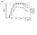
一方、微粒子33の粒径が大きいと散乱が大きくなり、逆効果となることから、光の波長である400〜800nmに比べて十分小さくする必要がある。具体的には、微粒子33の粒径は50nm以下、望ましくは10〜20nmとする。これは、図2に示すように、シリコーン樹脂(屈折率n3)中に分散された微粒子(屈折率n2)の大きさが50nm以下になると、樹脂封止部30においては可視光に対しては粒子界面での散乱等がなくなり、あたかもバルク樹脂と微粒子33が混合されたバルク材料としての特性を示すことによるものである。なお、図2は封止樹脂部30の厚さが600nm、光の波長が500nmである場合を示し、a=0.1〜0.4でデータをとっている。 On the other hand, if the particle size of the
このときのバルク材料、すなわち樹脂封止部30全体の屈折率n0は、シリコーン樹脂31に対する微粒子33の体積混合割合をaとして、n0=√(a・n22+(1−a)n32)となる。バルク材料の屈折率n0と蛍光体32の屈折率n1とを等しくすれば、散乱が起こらないため、光の取り出し効率が向上する。したがって、n12=a・n22+(1−a)n32という条件と、n2>n1>n3という条件を満たせばよい。The refractive index n0 of the bulk material, that is, the entire
上述したことから、微粒子33として粒径30nmのTiO2(屈折率n2=2.7)を用い、樹脂にシリコーン(屈折率n3=1.44)を用いれば、a=0.22のときnx=1.8となる。蛍光体32としてCe:YAG(n1=1.8)を用いれば、蛍光体32による散乱を最小限に抑えることができる。From the above, if TiO2 (refractive index n2 = 2.7) having a particle size of 30 nm is used as the
さらに、LED基板20(屈折率1.77)と、封止樹脂部30(屈折率1.8)とで屈折率の差が小さく、LED基板20と封止樹脂部30との間で発生する反射を最小限に抑えることができる。 Furthermore, the difference in refractive index between the LED substrate 20 (refractive index 1.77) and the sealing resin portion 30 (refractive index 1.8) is small, and is generated between the
上述したように、本第1実施の形態に係るLEDランプ10によれば、樹脂封止部30における蛍光体32による散乱を最小限に抑えることができるとともに、LED基板20と封止樹脂部30との間で発生する反射を最小限に抑えることができ、LED基板20からの外部への光の取り出し効率を上げることが可能である。また、樹脂中に微粒子を添加することで屈折率を調整しているので、製造コストも低く、技術的な困難度も低い。 As described above, according to the
図3は本発明の第2の実施の形態に係るLEDランプ40を模式的に示す断面図である。LEDランプ40は、LED基板50と、このLED基板50を封止する封止樹脂部60とを備えている。LED基板50は、サファイア基板(屈折率n4=1.77)から形成され、InGaN系活性層に形成された波長460〜480nmの青色、または360〜400nmの紫外線を発生する。封止樹脂部60は、シリコーン樹脂61と、このシリコーン樹脂31に添加された微粒子62から形成されている。微粒子62は、直径30nmのTiO2である。FIG. 3 is a cross-sectional view schematically showing an
シリコーン樹脂61(屈折率n6)中に分散された微粒子62(屈折率n5)の大きさが50nm以下になると、可視光に対しては粒子界面での散乱等がなくなり、あたかもバルク樹脂と微粒子が混合されたバルク材料としての特性を示す。そのときのバルク材料の屈折率nyは体積混合割合をaとして、ny2=(a・n52+(1−a)n62)となる。When the size of the fine particles 62 (refractive index n5) dispersed in the silicone resin 61 (refractive index n6) is 50 nm or less, there is no scattering at the particle interface with respect to visible light. The characteristic as a mixed bulk material is shown. At this time, the refractive index ny of the bulk material is ny2 = (a · n52 + (1−a) n62 ), where a is a volume mixing ratio.
バルク材料、すなわち樹脂封止部60の屈折率nyと、LED基板50の屈折率n4=1.77を近似させれば、LED基板50と封止樹脂部60との界面での全反射がなくなり、LED基板50から封止樹脂部60中への光取り出し効率が向上する。したがって、n42=a・n52+(1−a)n52という条件と、n5>n6という条件を満たせばよい。If the refractive index ny of the bulk material, that is, the
微粒子62として粒径30nmのTiO2(n5=2.7)を用い、樹脂にシリコーン(n6=1.44)を用いた場合、微粒子62の体積濃度を20%(a=0.2)とすることで、すなわち封止樹脂部60の屈折率をny=1.77とすることができ、これはLED基板50の屈折率n4と近似する。When TiO2 (n5 = 2.7) having a particle size of 30 nm is used as the
上述したように、本第2実施の形態に係るLEDランプ40によれば、LED基板50(屈折率1.77)と、封止樹脂部60(屈折率が1.8)とで屈折率の差を小さくすることで、LED基板50と封止樹脂部60との間で発生する反射を最小限に抑えることができる。また、樹脂中に微粒子を添加することで屈折率を調整しているので、製造コストも低く、技術的な困難度も低い。 As described above, according to the
なお、上述した各実施の形態では、微粒子33,62としてはTiO2を用いたが、屈折率が2.0のZrO2(酸化ジルコニウム)、ZnO(酸化亜鉛)、HfO2(酸化ハフニウム)や1.7のAl2O3(酸化アルミニウム)等を使用しても良い。In each of the above-described embodiments, TiO2 is used as the
なお、本発明は上記実施形態そのままに限定されるものではなく、実施段階ではその要
旨を逸脱しない範囲で構成要素を変形して具体化できる。また、上記実施形態に開示されている複数の構成要素の適宜な組み合わせにより、種々の発明を形成できる。例えば、実施形態に示される全構成要素から幾つかの構成要素を削除してもよい。さらに、異なる実施形態にわたる構成要素を適宜組み合わせてもよい。Note that the present invention is not limited to the above-described embodiment as it is, and can be embodied by modifying the constituent elements without departing from the scope of the invention in the implementation stage. In addition, various inventions can be formed by appropriately combining a plurality of components disclosed in the embodiment. For example, some components may be deleted from all the components shown in the embodiment. Furthermore, constituent elements over different embodiments may be appropriately combined.
10,40…LEDランプ(発光装置)、20,50…LED基板、30,60…封止樹脂部、31,61…シリコーン樹脂、32…蛍光体、33,62…微粒子。 DESCRIPTION OF
Claims (5)
Translated fromJapaneseこの発光素子基板を封止するとともに、屈折率n1の蛍光体と、屈折率n2の微粒子が添加された屈折率n3の樹脂を有する封止樹脂部とを備え、
上記屈折率n1〜n3は、n2>n1>n3の関係にあり、
上記微粒子の粒径は、上記発光素子基板の発する光の波長の1/10以下であることを特徴とする発光装置。A light emitting element substrate;
The light emitting element substrate is sealed, and includes a phosphor having a refractive index n1, and a sealing resin portion having a resin having a refractive index n3 to which fine particles having a refractive index n2 are added.
The refractive indexes n1 to n3 are in a relationship of n2>n1> n3,
The light-emitting device, wherein a particle diameter of the fine particles is 1/10 or less of a wavelength of light emitted from the light-emitting element substrate.
この発光素子基板を封止するとともに、屈折率n5の微粒子が添加された屈折率n6の樹脂を有する封止樹脂部とを備え、
上記屈折率n5及びn6は、n5>n6の関係にあり、
上記樹脂に対する上記微粒子の体積割合aが、n42=a・n52+(1−a)n52を満たすことを特徴とする発光装置。A light emitting element substrate having a refractive index n4;
Sealing the light emitting element substrate, and including a sealing resin portion having a refractive index n6 resin to which fine particles of a refractive index n5 are added,
The refractive indexes n5 and n6 have a relationship of n5> n6,
Volume ratio a of the fine particles to the resinis, the light emitting device and satisfies then4 2 = a · n5 2 + (1-a) n5 2.
Priority Applications (5)
| Application Number | Priority Date | Filing Date | Title |
|---|---|---|---|
| JP2005236006AJP2007053170A (en) | 2005-08-16 | 2005-08-16 | Light emitting device |
| US11/464,383US7345319B2 (en) | 2005-08-16 | 2006-08-14 | Light emitting device |
| CNB200610121510XACN100413107C (en) | 2005-08-16 | 2006-08-16 | Light emitting device |
| EP06017033AEP1755174A3 (en) | 2005-08-16 | 2006-08-16 | Light emitting device |
| TW095130017ATWI308403B (en) | 2005-08-16 | 2006-08-16 | Light emitting device |
Applications Claiming Priority (1)
| Application Number | Priority Date | Filing Date | Title |
|---|---|---|---|
| JP2005236006AJP2007053170A (en) | 2005-08-16 | 2005-08-16 | Light emitting device |
Related Child Applications (1)
| Application Number | Title | Priority Date | Filing Date |
|---|---|---|---|
| JP2010020623ADivisionJP2010098335A (en) | 2010-02-01 | 2010-02-01 | Light-emitting device |
Publications (1)
| Publication Number | Publication Date |
|---|---|
| JP2007053170Atrue JP2007053170A (en) | 2007-03-01 |
Family
ID=37434250
Family Applications (1)
| Application Number | Title | Priority Date | Filing Date |
|---|---|---|---|
| JP2005236006APendingJP2007053170A (en) | 2005-08-16 | 2005-08-16 | Light emitting device |
Country Status (5)
| Country | Link |
|---|---|
| US (1) | US7345319B2 (en) |
| EP (1) | EP1755174A3 (en) |
| JP (1) | JP2007053170A (en) |
| CN (1) | CN100413107C (en) |
| TW (1) | TWI308403B (en) |
Cited By (6)
| Publication number | Priority date | Publication date | Assignee | Title |
|---|---|---|---|---|
| JP2012089652A (en)* | 2010-10-19 | 2012-05-10 | Panasonic Corp | Semiconductor light emitting device |
| JP2013105947A (en)* | 2011-11-15 | 2013-05-30 | Toyo Ink Sc Holdings Co Ltd | Light-emitting device |
| JP2013105946A (en)* | 2011-11-15 | 2013-05-30 | Toyo Ink Sc Holdings Co Ltd | Light-emitting device |
| JP2013232479A (en)* | 2012-04-27 | 2013-11-14 | Toshiba Corp | Semiconductor light-emitting device |
| JP2016092271A (en)* | 2014-11-06 | 2016-05-23 | シャープ株式会社 | Phosphor sheet and lighting device |
| KR101862865B1 (en)* | 2011-07-18 | 2018-05-31 | 엘지이노텍 주식회사 | Optical member and display device having the same |
Families Citing this family (15)
| Publication number | Priority date | Publication date | Assignee | Title |
|---|---|---|---|---|
| WO2007018039A1 (en)* | 2005-08-05 | 2007-02-15 | Matsushita Electric Industrial Co., Ltd. | Semiconductor light-emitting device |
| JP4751269B2 (en)* | 2006-08-09 | 2011-08-17 | セイコーインスツル株式会社 | Illumination device, display device including the same, and portable electronic device |
| US8748922B2 (en)* | 2007-09-04 | 2014-06-10 | Koninklijke Philips N.V. | Light output device |
| US20090154198A1 (en)* | 2007-12-14 | 2009-06-18 | Joo Hoon Lee | Reflection type display apparatus |
| RU2567915C2 (en) | 2009-08-12 | 2015-11-10 | Конинклейке Филипс Электроникс Н.В. | Optical composition |
| CN101719533B (en)* | 2009-11-27 | 2015-12-09 | 晶能光电(江西)有限公司 | Charactron containing fluorescent material and manufacture method thereof |
| KR101713087B1 (en)* | 2010-02-19 | 2017-03-07 | 도레이 카부시키가이샤 | Phosphor-containing cured silicone, process for production of same, phosphor-containing silicone composition, precursor of the composition, sheet-shaped moldings, led package, light-emitting device, and process for production of led-mounted substrate |
| KR20130083388A (en)* | 2010-05-20 | 2013-07-22 | 다리엔 루밍라이트 컴퍼니 리미티드 | A peelable light conversion luminescent film |
| US9117979B2 (en) | 2010-12-13 | 2015-08-25 | Toray Industries, Inc. | Phosphor sheet, LED and light emitting device using the same and method for manufacturing LED |
| DE102011009369A1 (en)* | 2011-01-25 | 2012-07-26 | Osram Opto Semiconductors Gmbh | Optoelectronic semiconductor chip and method for its production |
| WO2013175773A1 (en)* | 2012-05-22 | 2013-11-28 | パナソニック株式会社 | Wavelength conversion element and method for manufacturing same, as well as led element and semiconductor laser emission device using wavelength conversion element |
| US20150171372A1 (en)* | 2012-07-04 | 2015-06-18 | Sharp Kabushiki Kaisha | Fluorescent material, fluorescent coating material, phosphor substrate, electronic apparatus, and led package |
| US10106666B2 (en) | 2016-03-02 | 2018-10-23 | Samsung Electronics Co., Ltd. | Curable silicone resin composition containing inorganic oxide and optical member using same |
| CN107450261B (en)* | 2016-05-31 | 2021-02-05 | 佳能株式会社 | Wavelength conversion element, light source device, and image projection device |
| CN108611045A (en)* | 2018-04-19 | 2018-10-02 | 武汉华星光电技术有限公司 | Fluorescent glue and preparation method thereof, backlight module |
Citations (1)
| Publication number | Priority date | Publication date | Assignee | Title |
|---|---|---|---|---|
| JP2004015063A (en)* | 2002-06-07 | 2004-01-15 | Lumileds Lighting Us Llc | Light-emitting device using nanoparticles |
Family Cites Families (11)
| Publication number | Priority date | Publication date | Assignee | Title |
|---|---|---|---|---|
| US5777433A (en)* | 1996-07-11 | 1998-07-07 | Hewlett-Packard Company | High refractive index package material and a light emitting device encapsulated with such material |
| JP3065544B2 (en)* | 1996-12-06 | 2000-07-17 | スタンレー電気株式会社 | LED lamp with fluorescent agent |
| DE19964252A1 (en)* | 1999-12-30 | 2002-06-06 | Osram Opto Semiconductors Gmbh | Surface mount component for an LED white light source |
| US6777871B2 (en)* | 2000-03-31 | 2004-08-17 | General Electric Company | Organic electroluminescent devices with enhanced light extraction |
| JP2003101078A (en)* | 2001-09-25 | 2003-04-04 | Toyoda Gosei Co Ltd | Light-emitting device |
| JP2003243727A (en) | 2001-12-14 | 2003-08-29 | Nichia Chem Ind Ltd | Light emitting apparatus |
| JP4360788B2 (en)* | 2002-08-29 | 2009-11-11 | シチズン電子株式会社 | Backlight for liquid crystal display panel and method of manufacturing light emitting diode used therefor |
| JP4661032B2 (en) | 2003-06-26 | 2011-03-30 | 日亜化学工業株式会社 | Light emitting device and manufacturing method thereof |
| JP2005064233A (en)* | 2003-08-12 | 2005-03-10 | Stanley Electric Co Ltd | Wavelength conversion type LED |
| WO2005027576A2 (en)* | 2003-09-08 | 2005-03-24 | Nanocrystal Lighting Corporation | Light efficient packaging configurations for led lamps using high refractive index encapsulants |
| CN1638585A (en)* | 2003-12-26 | 2005-07-13 | 日东电工株式会社 | Electroluminescence device, planar light source and display using the same |
- 2005
- 2005-08-16JPJP2005236006Apatent/JP2007053170A/enactivePending
- 2006
- 2006-08-14USUS11/464,383patent/US7345319B2/ennot_activeExpired - Fee Related
- 2006-08-16CNCNB200610121510XApatent/CN100413107C/ennot_activeExpired - Fee Related
- 2006-08-16EPEP06017033Apatent/EP1755174A3/ennot_activeWithdrawn
- 2006-08-16TWTW095130017Apatent/TWI308403B/ennot_activeIP Right Cessation
Patent Citations (1)
| Publication number | Priority date | Publication date | Assignee | Title |
|---|---|---|---|---|
| JP2004015063A (en)* | 2002-06-07 | 2004-01-15 | Lumileds Lighting Us Llc | Light-emitting device using nanoparticles |
Cited By (7)
| Publication number | Priority date | Publication date | Assignee | Title |
|---|---|---|---|---|
| JP2012089652A (en)* | 2010-10-19 | 2012-05-10 | Panasonic Corp | Semiconductor light emitting device |
| KR101862865B1 (en)* | 2011-07-18 | 2018-05-31 | 엘지이노텍 주식회사 | Optical member and display device having the same |
| JP2013105947A (en)* | 2011-11-15 | 2013-05-30 | Toyo Ink Sc Holdings Co Ltd | Light-emitting device |
| JP2013105946A (en)* | 2011-11-15 | 2013-05-30 | Toyo Ink Sc Holdings Co Ltd | Light-emitting device |
| JP2013232479A (en)* | 2012-04-27 | 2013-11-14 | Toshiba Corp | Semiconductor light-emitting device |
| US9246069B2 (en) | 2012-04-27 | 2016-01-26 | Kabushiki Kaisha Toshiba | Semiconductor light emitting device |
| JP2016092271A (en)* | 2014-11-06 | 2016-05-23 | シャープ株式会社 | Phosphor sheet and lighting device |
Also Published As
| Publication number | Publication date |
|---|---|
| US20070041191A1 (en) | 2007-02-22 |
| TWI308403B (en) | 2009-04-01 |
| US7345319B2 (en) | 2008-03-18 |
| CN1917243A (en) | 2007-02-21 |
| EP1755174A2 (en) | 2007-02-21 |
| CN100413107C (en) | 2008-08-20 |
| EP1755174A3 (en) | 2010-08-25 |
| TW200715619A (en) | 2007-04-16 |
Similar Documents
| Publication | Publication Date | Title |
|---|---|---|
| JP2007053170A (en) | Light emitting device | |
| TWI589034B (en) | Phosphor conversion light-emitting diodes, lamps and lamps | |
| JP2017027019A (en) | Light source device | |
| JP2007180507A (en) | White light emitting device | |
| JP6457225B2 (en) | Light emitting device | |
| TW201535797A (en) | Illuminating device | |
| JP2013102078A (en) | Light source device and luminaire | |
| JP6140730B2 (en) | Method for creating phosphor layer | |
| CN104756251A (en) | Light-emitting diode module | |
| JP2013207049A (en) | Light emitting device using wavelength conversion body | |
| CN102705724A (en) | Light cavity that improves light output uniformity | |
| JP2008078225A (en) | Light emitting device | |
| JP6723939B2 (en) | Wavelength conversion element, light source device, and image projection device | |
| JP2013168602A (en) | Light source device and luminaire | |
| JP2013038353A (en) | Light-emitting module | |
| JP6337919B2 (en) | Optical component and light emitting device | |
| JP5558986B2 (en) | LED lamp | |
| JP2007134606A (en) | White light source | |
| JP2007220432A (en) | Light-emitting device | |
| JP2010098335A (en) | Light-emitting device | |
| JP4926303B1 (en) | Light emitting device and lamp | |
| JP2008305748A (en) | Bulb type fluorescent lamp | |
| JP2006091532A (en) | Ultraviolet cut member, lamp and lighting fixture | |
| JP2008507839A (en) | Photonic bandgap material with built-in phosphor | |
| KR100807015B1 (en) | Light emitting device |
Legal Events
| Date | Code | Title | Description |
|---|---|---|---|
| A621 | Written request for application examination | Free format text:JAPANESE INTERMEDIATE CODE: A621 Effective date:20080711 | |
| A131 | Notification of reasons for refusal | Free format text:JAPANESE INTERMEDIATE CODE: A131 Effective date:20090818 | |
| A521 | Request for written amendment filed | Free format text:JAPANESE INTERMEDIATE CODE: A523 Effective date:20091019 | |
| A131 | Notification of reasons for refusal | Free format text:JAPANESE INTERMEDIATE CODE: A131 Effective date:20091201 | |
| A521 | Request for written amendment filed | Free format text:JAPANESE INTERMEDIATE CODE: A523 Effective date:20100201 | |
| A02 | Decision of refusal | Free format text:JAPANESE INTERMEDIATE CODE: A02 Effective date:20100511 |