JP2007052368A - Liquid crystal display device - Google Patents
Liquid crystal display deviceDownload PDFInfo
- Publication number
- JP2007052368A JP2007052368AJP2005239044AJP2005239044AJP2007052368AJP 2007052368 AJP2007052368 AJP 2007052368AJP 2005239044 AJP2005239044 AJP 2005239044AJP 2005239044 AJP2005239044 AJP 2005239044AJP 2007052368 AJP2007052368 AJP 2007052368A
- Authority
- JP
- Japan
- Prior art keywords
- electrode
- substrate
- liquid crystal
- counter
- array substrate
- Prior art date
- Legal status (The legal status is an assumption and is not a legal conclusion. Google has not performed a legal analysis and makes no representation as to the accuracy of the status listed.)
- Pending
Links
- 239000004973liquid crystal related substanceSubstances0.000titleclaimsabstractdescription85
- 239000000758substrateSubstances0.000claimsabstractdescription265
- 239000011159matrix materialSubstances0.000claimsdescription10
- 238000007667floatingMethods0.000abstractdescription2
- 238000007790scrapingMethods0.000abstract1
- 239000010408filmSubstances0.000description136
- 239000010410layerSubstances0.000description92
- 239000011521glassSubstances0.000description47
- 239000010409thin filmSubstances0.000description28
- 125000006850spacer groupChemical group0.000description23
- 239000011229interlayerSubstances0.000description17
- 239000000463materialSubstances0.000description17
- 230000002093peripheral effectEffects0.000description10
- 238000007789sealingMethods0.000description10
- 239000004925Acrylic resinSubstances0.000description9
- 229920000178Acrylic resinPolymers0.000description9
- 239000000203mixtureSubstances0.000description9
- 238000000034methodMethods0.000description7
- 239000004065semiconductorSubstances0.000description7
- 235000010724Wisteria floribundaNutrition0.000description6
- 239000011347resinSubstances0.000description6
- 229920005989resinPolymers0.000description6
- 239000003566sealing materialSubstances0.000description6
- NIXOWILDQLNWCW-UHFFFAOYSA-Nacrylic acid groupChemical groupC(C=C)(=O)ONIXOWILDQLNWCW-UHFFFAOYSA-N0.000description5
- 239000000853adhesiveSubstances0.000description5
- 239000003990capacitorSubstances0.000description5
- 230000007704transitionEffects0.000description5
- YEJRWHAVMIAJKC-UHFFFAOYSA-N4-ButyrolactoneChemical compoundO=C1CCCO1YEJRWHAVMIAJKC-UHFFFAOYSA-N0.000description4
- 230000001070adhesive effectEffects0.000description4
- 229910021417amorphous siliconInorganic materials0.000description4
- 230000007547defectEffects0.000description4
- 238000004519manufacturing processMethods0.000description4
- 238000000059patterningMethods0.000description4
- 239000007864aqueous solutionSubstances0.000description3
- 238000002347injectionMethods0.000description3
- 239000007924injectionSubstances0.000description3
- 229910021420polycrystalline siliconInorganic materials0.000description3
- 229920005591polysiliconPolymers0.000description3
- 230000008569processEffects0.000description3
- BQCADISMDOOEFD-UHFFFAOYSA-NSilverChemical compound[Ag]BQCADISMDOOEFD-UHFFFAOYSA-N0.000description2
- 230000008859changeEffects0.000description2
- 230000000694effectsEffects0.000description2
- 239000002245particleSubstances0.000description2
- 239000000049pigmentSubstances0.000description2
- 239000001054red pigmentSubstances0.000description2
- 239000000565sealantSubstances0.000description2
- 229910052709silverInorganic materials0.000description2
- 239000004332silverSubstances0.000description2
- 238000004544sputter depositionMethods0.000description2
- 239000004593EpoxySubstances0.000description1
- KWYUFKZDYYNOTN-UHFFFAOYSA-MPotassium hydroxideChemical compound[OH-].[K+]KWYUFKZDYYNOTN-UHFFFAOYSA-M0.000description1
- 229910052581Si3N4Inorganic materials0.000description1
- VYPSYNLAJGMNEJ-UHFFFAOYSA-NSilicium dioxideChemical compoundO=[Si]=OVYPSYNLAJGMNEJ-UHFFFAOYSA-N0.000description1
- 238000000137annealingMethods0.000description1
- 239000011324beadSubstances0.000description1
- 239000011230binding agentSubstances0.000description1
- 239000001055blue pigmentSubstances0.000description1
- 239000003795chemical substances by applicationSubstances0.000description1
- 239000003086colorantSubstances0.000description1
- 238000002425crystallisationMethods0.000description1
- 230000008025crystallizationEffects0.000description1
- 230000006866deteriorationEffects0.000description1
- 238000010586diagramMethods0.000description1
- 238000004090dissolutionMethods0.000description1
- 239000005262ferroelectric liquid crystals (FLCs)Substances0.000description1
- 239000012634fragmentSubstances0.000description1
- 239000001056green pigmentSubstances0.000description1
- 238000010438heat treatmentMethods0.000description1
- AMGQUBHHOARCQH-UHFFFAOYSA-Nindium;oxotinChemical compound[In].[Sn]=OAMGQUBHHOARCQH-UHFFFAOYSA-N0.000description1
- 239000011810insulating materialSubstances0.000description1
- 230000001678irradiating effectEffects0.000description1
- 238000007645offset printingMethods0.000description1
- 230000003287optical effectEffects0.000description1
- 238000000206photolithographyMethods0.000description1
- 239000004033plasticSubstances0.000description1
- 238000007639printingMethods0.000description1
- 230000001105regulatory effectEffects0.000description1
- 230000004044responseEffects0.000description1
- HQVNEWCFYHHQES-UHFFFAOYSA-Nsilicon nitrideChemical compoundN12[Si]34N5[Si]62N3[Si]51N64HQVNEWCFYHHQES-UHFFFAOYSA-N0.000description1
- 229910052814silicon oxideInorganic materials0.000description1
- 239000002904solventSubstances0.000description1
- 238000005507sprayingMethods0.000description1
- 229920001187thermosetting polymerPolymers0.000description1
Images


Landscapes
- Liquid Crystal (AREA)
- Position Input By Displaying (AREA)
Abstract
Description
Translated fromJapanese本発明は、アレイ基板と対向基板との間に突条電極を有する液晶表示装置に関する。 The present invention relates to a liquid crystal display device having a protruding electrode between an array substrate and a counter substrate.
従来、この種の液晶表示装置は、アレイ基板と対向基板との間に液晶が介在されており、これらアレイ基板と対向基板と周囲の液晶封入口を除いた部分が接着剤にて固定され、この液晶封入口が封止剤で封止されている。さらに、これらアレイ基板と対向基板との間には、これらアレイ基板と対向基板との間の距離を一定に保持するために粒径の均一なプラスティックビーズなどがスペーサとして散在されている。 Conventionally, in this type of liquid crystal display device, liquid crystal is interposed between the array substrate and the counter substrate, and the portions excluding the array substrate, the counter substrate, and the surrounding liquid crystal sealing port are fixed with an adhesive, The liquid crystal sealing port is sealed with a sealant. Furthermore, between the array substrate and the counter substrate, plastic beads having a uniform particle diameter are scattered as spacers in order to keep the distance between the array substrate and the counter substrate constant.
また、カラー表示用の液晶表示装置は、アレイ基板と対向基板のいずれか一方のガラス基板上に、R(Red:赤色)に着色された赤色層と、G(Green:緑色)に着色された緑色層と、B(Blue:青色)に着色された青色層とで構成されたカラーフィルタ層が形成されている。そして、この液晶表示装置の表示方式としては、例えばTN(Twisted Nematic)形、ST(Stock Time)形、GH(Guest Host)形あるいはECB(Electrically Controlled Birefringence)形や強誘電性液晶などが用いられている。また、封止剤としては、例えば熱にて硬化する熱硬化型や紫外線の照射にて硬化する紫外線硬化型のアクリル形またはエポキシ形の接着剤などが用いられている。 In addition, the liquid crystal display device for color display is colored in a red layer colored R (Red) and G (Green) on one of the glass substrate of the array substrate and the counter substrate. A color filter layer composed of a green layer and a blue layer colored B (Blue) is formed. As a display method of this liquid crystal display device, for example, TN (Twisted Nematic) type, ST (Stock Time) type, GH (Guest Host) type, ECB (Electrically Controlled Birefringence) type, ferroelectric liquid crystal, etc. are used. ing. Further, as the sealant, for example, a thermosetting type curable by heat or an ultraviolet curable type acrylic or epoxy type adhesive curable by ultraviolet irradiation is used.
さらに、カラー型アクティブマトリクス駆動液晶表示装置は、絶縁基板上に走査線および信号線が格子状に設けられ、これら走査線および信号線の交点に対応してアモルファスシリコン(a−Si)を半導体層とした薄膜トランジスタ(Thin Film Transistor:TFT)が設けられ、これら薄膜トランジスタに画素電極が電気的に接続されたアクティブマトリクス基板としてのアレイ基板を備えている。そして、このアレイ基板に対向して、対向電極が設けられた対向電極が配設されており、この対向基板上にカラーフィルタ層が設けられている。 Further, in the color type active matrix drive liquid crystal display device, scanning lines and signal lines are provided in a lattice pattern on an insulating substrate, and amorphous silicon (a-Si) is applied to the semiconductor layer corresponding to the intersections of these scanning lines and signal lines. A thin film transistor (TFT) is provided, and an array substrate is provided as an active matrix substrate in which pixel electrodes are electrically connected to the thin film transistor. A counter electrode provided with a counter electrode is disposed opposite to the array substrate, and a color filter layer is provided on the counter substrate.
また、これらアレイ基板と対向基板との間の画面周辺部には、アレイ基板から対向基板へ電圧を印加するトランスファである電極転移材が配置されている。この電極転移材としては、導電性の銀粒子をバインダにてペースト状にした銀ペーストなどが用いられる。そして、この電極転移材によって、アレイ基板と対向基板とが電気的に接続されている。また、これらアレイ基板と対向基板とのそれぞれは偏光板にて挟持されており、光シャッタとしてカラー画像が表示可能に構成されている。 In addition, an electrode transfer material, which is a transfer for applying a voltage from the array substrate to the counter substrate, is disposed at the periphery of the screen between the array substrate and the counter substrate. As the electrode transition material, a silver paste or the like in which conductive silver particles are pasted with a binder is used. The array substrate and the counter substrate are electrically connected by this electrode transition material. Each of the array substrate and the counter substrate is sandwiched between polarizing plates, and is configured to display a color image as an optical shutter.
さらに、タッチパネルと呼ばれるセンサ機能を有する液晶表示装置は、この液晶表示装置の外部にセンサ機能を有する構成が設けられている。例えば、この液晶表示装置の画面上にセンサ機能を有する別のシート状のパネルを対向させて配置することによって、この液晶表示装置をタッチパネルとして利用可能とさせた構成が知られている(例えば、特許文献1参照。)。 Further, a liquid crystal display device having a sensor function called a touch panel is provided with a configuration having a sensor function outside the liquid crystal display device. For example, there is known a configuration in which the liquid crystal display device can be used as a touch panel by disposing another sheet-like panel having a sensor function on the screen of the liquid crystal display device to face each other (for example, (See Patent Document 1).
ところが、このセンサ機能を有する液晶表示装置では、液晶表示装置の外部にセンサ機能を有するシート状のパネルが対向させて配置されているため、このパネルの厚さほど液晶表示装置が厚くなってしまうから、この液晶表示装置の明るさを低下させてしまう。また、この液晶表示装置のほかにセンサ機能を有するパネルが別途必要となるため、この液晶表示装置の製造コストが高くなってしまう。 However, in the liquid crystal display device having this sensor function, since the sheet-like panel having the sensor function is arranged opposite to the outside of the liquid crystal display device, the liquid crystal display device becomes thicker as the thickness of the panel. This will reduce the brightness of the liquid crystal display device. In addition to this liquid crystal display device, a panel having a sensor function is required separately, which increases the manufacturing cost of the liquid crystal display device.
そこで、この種のセンサ機能を有する液晶表示装置としては、互いに対向する側の一主面に絶縁性の配向膜がそれぞれ積層されたアレイ基板と対向基板との間のセルギャップ内に、このセルギャップより小さな突条のセンサが設けられており、このセンサもまた配向膜にて積層されている。そして、これらアレイ基板あるいは対向基板の任意の位置を押すことによってセンサが導通してスイッチングする構成が知られている(例えば、特許文献2参照。)。
しかしながら、上述したセンサ機能を有する液晶表示装置では、この液晶表示装置内にセンサを設けることが可能で、センサ機能を有するパネルが不要な分、厚さを小さくして明るさを向上できるが、この液晶表示装置のアレイ基板および対向基板それぞれの一主面に、絶縁性の配向膜が積層されているので、これらアレイ基板および対向基板を強く押せば配向膜を介してセンサを導通させてスイッチングできるものの、このセンサの表面の導電性が配向膜によって低下してしまう。 However, in the liquid crystal display device having the sensor function described above, it is possible to provide a sensor in the liquid crystal display device, and the brightness can be improved by reducing the thickness, because the panel having the sensor function is unnecessary. An insulating alignment film is laminated on each main surface of the array substrate and the counter substrate of this liquid crystal display device. If the array substrate and the counter substrate are pressed firmly, the sensor is turned on and switched through the alignment film. Although it is possible, the conductivity of the surface of the sensor is lowered by the alignment film.
また、アレイ基板および対向基板を押してセンサのスイッチングを繰り返すことによって、このセンサによる配向膜への接触が繰り返される。したがって、このセンサが接触する部分の配向膜が削れて、配向不良を起したり、削れた配向膜が液晶中を浮遊して表示不良を起したりするおそれがあるから、繰り返して使用することによって表示品位が維持できなくなるおそれがあるという問題を有している。 Further, by repeating the switching of the sensor by pushing the array substrate and the counter substrate, the contact with the alignment film by the sensor is repeated. Therefore, the alignment film at the part where the sensor comes into contact may be scraped to cause orientation failure, or the shaved orientation film may float in the liquid crystal and cause display failure. Therefore, the display quality may not be maintained.
本発明は、このような点に鑑みなされたもので、繰り返して使用しても高い表示品位を維持できる液晶表示装置を提供することを目的とする。 The present invention has been made in view of these points, and an object of the present invention is to provide a liquid crystal display device that can maintain high display quality even when used repeatedly.
本発明は、絶縁基板、この絶縁基板の一主面にマトリクス状に設けられた複数の画素、およびこれら複数の画素上に設けられた配向膜を備えたアレイ基板と、絶縁基板、この絶縁基板の一主面に設けられた電極層、およびこの電極層の一主面に設けられた配向膜を備え、この配向膜を前記アレイ基板の配向膜に対向させて配設された対向基板と、前記アレイ基板と対向基板との間に介在された液晶とを具備し、前記アレイ基板および対向基板のいずれか一方の対向する側の前記絶縁基板の一主面とこの一主面に設けられた前記配向膜との間には、この一主面より突出し前記対向基板の電極層への電気的な接触によってスイッチングする突条電極が設けられ、前記アレイ基板の配向膜および前記対向基板の配向膜の少なくとも一方は、前記突条電極と前記電極層とが対向する部分を除いて設けられているものである。 The present invention relates to an insulating substrate, a plurality of pixels provided in a matrix on one main surface of the insulating substrate, an array substrate including an alignment film provided on the plurality of pixels, an insulating substrate, and the insulating substrate. An electrode layer provided on one main surface and an alignment film provided on one main surface of the electrode layer, and a counter substrate disposed so that the alignment film faces the alignment film of the array substrate; A liquid crystal interposed between the array substrate and the counter substrate, and provided on one main surface of the insulating substrate on one side of the array substrate and the counter substrate, and on the one main surface. Between the alignment films, there are provided projecting electrodes protruding from the one main surface and switching by electrical contact with the electrode layer of the counter substrate, and the alignment film of the array substrate and the alignment film of the counter substrate At least one of the protrusions And poles To the electrode layer is one that is provided except for a portion opposite.
そして、アレイ基板および対向基板のいずれか一方の対向する側の絶縁基板の一主面とこの一主面に設けた配向膜との間に突条電極を設け、アレイ基板の絶縁基板の一主面に設けた配向膜と、対向基板の絶縁基板の一主面に設けた配向膜の少なくとも一方を、突条電極と電極層とが対向する部分を除いて設けたことにより、突条電極を電極層に電気的に接触させてスイッチングさせた際に、この突条電極が少なくとも一方の配向膜に接触しなくなる。したがって、これら突条電極と電極層とを繰り返してスイッチングさせても、これら突条電極と電極層とのスイッチングによって少なくとも一方の配向膜が削れて配向不良が起きたり、この削れた配向膜が液晶中を浮遊して表示不良が起きたりしないので、これら突条電極と電極層とのスイッチングを繰り返しても高い表示品位を維持できる。 Then, a protruding electrode is provided between one main surface of the opposing insulating substrate of either the array substrate or the counter substrate and the alignment film provided on the one main surface, and the main substrate of the insulating substrate of the array substrate is provided. By providing at least one of the alignment film provided on the surface and the alignment film provided on one main surface of the insulating substrate of the counter substrate, excluding the portion where the protruding electrode and the electrode layer face each other, the protruding electrode is provided. When the electrode layer is electrically contacted and switched, the protruding electrode does not contact at least one of the alignment films. Therefore, even if these protrusion electrodes and the electrode layer are repeatedly switched, at least one of the alignment films is scraped due to the switching between the protrusion electrodes and the electrode layer, resulting in poor alignment, or the scraped alignment film is liquid crystal Since display defects do not occur due to floating inside, high display quality can be maintained even if switching between the protruding electrodes and the electrode layers is repeated.
本発明によれば、アレイ基板の配向膜と対向基板の配向膜の少なくとも一方を、突条電極と電極層とが対向する部分を除いて設けたことにより、この突条電極を電極層に電気的に接触させてスイッチングさせた際に、この突条電極が少なくとも一方の配向膜に接触しなくなる。したがって、これら突条電極と電極層とを繰り返してスイッチングさせても、少なくとも一方の配向膜が削れたりせず、配向不良や表示不良が起きたりしないから、これら突条電極と電極層とのスイッチングを繰り返しても高い表示品位を維持できる。 According to the present invention, at least one of the alignment film of the array substrate and the alignment film of the counter substrate is provided except for the portion where the protruding electrode and the electrode layer face each other, so that the protruding electrode is electrically connected to the electrode layer. When the contact electrode is switched by the contact, the protruding electrode does not contact at least one of the alignment films. Therefore, even if these protrusion electrodes and the electrode layer are repeatedly switched, at least one of the alignment films is not scraped, and alignment defects and display defects do not occur. Therefore, the switching between the protrusion electrodes and the electrode layers does not occur. High display quality can be maintained even if the operation is repeated.
以下、本発明の液晶表示装置の第1の実施の形態の構成を図1ないし図3を参照して説明する。 The configuration of the first embodiment of the liquid crystal display device of the present invention will be described below with reference to FIGS.
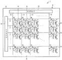
図1および図2において、1は平面表示装置としての液晶パネルで、この液晶パネル1は、タッチパネルセンサが内蔵された液晶表示装置であるとともに、スイッチング素子として薄膜トランジスタ(Thin Film Transistor:TFT)を用いたアクティブマトリクス型の液晶表示素子である。そして、この液晶パネル1は、アクティブマトリクス基板としての略矩形平板状のアレイ基板2を備えている。このアレイ基板2は、XGA(eXtended Graphics Array)型の薄膜トランジスタ(TFT)基板であって、略透明な矩形平板状の絶縁基板としての透光性基板であるガラス基板3を有している。 1 and 2,
このガラス基板3の一主面である表面上の中央部には、図2に示すように、画像表示領域としての画面部4が形成されている。そして、この画面部4には、複数の画素5がマトリクス状に設けられて配置されている。これら複数の画素5は、ガラス基板3の縦方向に沿ってn個形成されており、このガラス基板3の横方向に沿ってm個形成されている。したがって、これら複数の画素5は、ガラス基板3上にn×m個形成されている。さらに、これら画素5のそれぞれには、表示電極としての画素電極6、蓄積容量としての画素補助容量である補助容量7、および薄膜トランジスタ8がそれぞれ1つずつ配置されている。 As shown in FIG. 2, a
また、ガラス基板3の表面には、ゲート電極配線としての複数の走査線11が、このガラス基板3の幅方向に沿って配設されている。これら走査線11は、ガラス基板3の横方向に向けて等間隔に平行に離間されている。また、これら走査線11間のそれぞれには、電極配線としての画像信号配線である複数の信号線12が、ガラス基板3の縦方向に沿って配設されている。これら信号線12は、ガラス基板3の横方向に向けて等間隔に平行に離間されている。したがって、これら走査線11および信号線12は、ガラス基板3上に交差して格子状であるマトリクス状に配線されている。そして、これら走査線11および信号線12の各交点に対応して、画素電極6、補助容量7および薄膜トランジスタ8のそれぞれが各画素5毎に設けられている。 A plurality of
一方、ガラス基板3の周縁には、信号線駆動回路としての細長矩形平板状のYドライバ回路14が配設されている。このYドライバ回路14は、ガラス基板3の横方向に沿った一側縁に設けられている。さらに、このYドライバ回路14は、ガラス基板3の縦方向に沿って設けられており、このガラス基板3上の各走査線11それぞれの一端部が電気的に接続されている。 On the other hand, on the peripheral edge of the
また、このガラス基板3の縦方向に沿った一端には、走査線駆動回路としての細長矩形平板状のXドライバ回路15が配設されている。このXドライバ回路15は、ガラス基板3の横方向に沿って設けられており、このガラス基板3上の各信号線12それぞれの一端部が電気的に接続されている。なお、これらYドライバ回路14およびXドライバ回路15は、Yドライバ回路14から各走査線11に供給される走査信号によって、薄膜トランジスタ8をオンオフさせるタイミングに同期して、Xドライバ回路15から各信号線12に画素信号を供給させることによって、アレイ基板2の画面部4に所定の画像を表示させる。 Further, an
次いで、図1に示すように、ガラス基板3の表面には、シリコン窒化膜や酸化シリコン膜などにて構成された図示しないアンダーコート層が積層されて成膜されている。このアンダーコート層上には、トップゲート型構造としてのトップゲートタイプである薄膜トランジスタ8が1画素構成要素として配設されている。この薄膜トランジスタ8は、スイッチング素子であるとともに半導体素子としてのTFT素子である。そして、これら薄膜トランジスタ8は、アンダーコート層上に積層されて形成されたソース電極21およびドレイン電極22を備えている。これらソース電極21およびドレイン電極22は、所定の間隙を介して電気的に絶縁された状態で設けられている。そして、このソース電極21は、信号線12に電気的に接続されており、ドレイン電極22は、補助容量7に電気的に接続されている。 Next, as shown in FIG. 1, an undercoat layer (not shown) made of a silicon nitride film, a silicon oxide film, or the like is laminated on the surface of the
さらに、これらソース電極21およびドレイン電極22の間には、半導体層としての活性層23が設けられている。この活性層23は、ソース電極21およびドレイン電極22を含むアンダーコート層上に設けられている。そして、この活性層23は、多結晶半導体としてのポリシリコン(p−Si)にて構成された多結晶半導体層としてのポリシリコン半導体層である。すなわち、この活性層23は、非晶質半導体としてのアモルファスシリコン(a−Si)をエキシマレーザ溶解結晶化でアニールしてからパターニングして作成した島状のポリシリコン薄膜である。 Further, an
また、この活性層23上には、導電性を有するゲート電極24が積層されて成膜されている。このゲート電極24は、図2に示すように、走査線11の一側縁に一体的に接続されて、この走査線11の一部を構成する。すなわち、このゲート電極24は、走査線11に電気的に接続されている。ここで、このゲート電極24は、活性層23の長手方向に直交する長手方向を有している。また、このゲート電極24は、活性層23の幅寸法より小さな幅寸法を有しており、この活性層23上の中央部に設けられている。 On the
そして、これら薄膜トランジスタ8を含むアンダーコート層上には、絶縁性を有する絶縁層としての層間絶縁膜25が積層されて形成されている。この層間絶縁膜25は、感光性アクリル樹脂にて形成されており、アレイ基板2の少なくとも画面部4の略全域を覆っている。そして、この層間絶縁膜25には、各薄膜トランジスタ8のドレイン電極22を開口させる導通部としてのコンタクトホール26が形成されている。これらコンタクトホール26は、各薄膜トランジスタ8のドレイン電極22を層間絶縁膜25上に導通させている。 On the undercoat layer including these
さらに、これらコンタクトホール26を含む層間絶縁膜25上には、ITO(Indium Tin Oxide)にて構成された透明な画素電極6が積層されて設けられている。この画素電極6は、各画素5に対応してアレイ基板2の画面部4にマトリクス状に設けられている。また、この画素電極6は、コンタクトホール26を介して薄膜トランジスタ8のドレイン電極22に導通されて電気的に接続されている。すなわち、この画素電極6は、この画素電極6にドレイン電極22が電気的に接続されている薄膜トランジスタ8によって制御される。 Further, a
また、画素電極6上の対向基板41のカラーフィルタ層43の各青色フィルタ部46に対向する位置には、アレイ基板2と対向基板41との間の間隔を保持する細長円柱状のスペーサ27が設けられている。これらスペーサ27は、感光性アクリル樹脂、例えばNN600(JSR株式会社製)にて形成されており、高さ5μmで平面視15μm×15μmの大きさに形成されている。そして、これらスペーサ27は、画面部4の縦方向および横方向のそれぞれに向けて所定個数、例えば2個の画素5を介した部分に位置する画素5毎に設けられている。すなわち、これらスペーサ27は、アレイ基板2の画面部4上に等間隔に離間されて設けられている。 In addition, in the position of the
さらに、これらスペーサ27は、絶縁性を有する材料にて形成されており、青色フィルタ部46が対向する画素5内の周縁部に設けられている。すなわち、これらスペーサ27は、開口率の低下を防止するために平面視で薄膜トランジスタ8からずれた位置に設けられている。すなわち、これらスペーサ27は、各画素5内において平面視でコンタクトホール26を介した薄膜トランジスタ8の反対側に設けられている。さらに、これらスペーサ27は、画素電極6と対向基板41の青色フィルタ部46との間のセルギャップとしてのセル厚Aに等しい高さ寸法を有している。 Further, these
さらに、この層間絶縁膜25上の対向基板41のカラーフィルタ層43に対向する位置には、センサ機能を有する突条のタッチセンサ30が設けられている。このタッチセンサ30は、層間絶縁膜25の一主面である表面より上方に突出した突条の第1の電極部としての突条電極31を備えている。この突条電極31は、スペーサ27の高さ寸法より小さな高さ寸法を有している。また、この突条電極31は、この突条電極31と対向基板41の対向電極47との間の距離の変化に基づく電気的な容量の変化でスイッチングする。言い換えると、これらタッチセンサ30は、突条電極31と対向電極47とによって構成されており、図3に示すように、対向基板41の裏面側を指Fなどで押して変形させて、この対向基板41の対向電極47と突条電極31との電気的な接触によってオンするセンサ機能を発揮する。そして、これら突条電極31は、アレイ基板2の画面部4上の画素5内の周縁部に設けられている。すなわち、これら突条電極31は、画素5内における平面視で薄膜トランジスタ8上に設けられている。そして、これら突条電極31は、アレイ基板2の画面部4の縦方向および横方向のそれぞれに沿って等間隔に離間されている。 Further, a
また、これら突条電極31は、アレイ基板2と対向基板41との間のセル厚Aより小さな高さ寸法を有している。具体的に、これら突条電極31は、対向基板41のカラーフィルタ層43との間に所定の間隙Bができるように形成されている。すなわち、これら突条電極31は、アレイ基板2の層間絶縁膜25と対向基板のカラーフィルタ層43との間のセル厚Aより小さな高さ寸法を有している。 The protruding
そして、これら突条電極31は、絶縁性を有する細長略角柱状の絶縁部としての突条のセンサ用突起32を備えている。このセンサ用突起32は、層間絶縁膜25上に下端面を当接させた状態で、この層間絶縁膜25上に積層されて設けられている。また、このセンサ用突起32は、スペーサ27と同じ材料で形成されている。具体的に、このセンサ用突起32は、感光性アクリル樹脂、例えばNN600(JSR株式会社製)にて、高さ3.5μmで平面視20μm×20μmの大きさに形成されている。 Each of the
さらに、このセンサ用突起32の上端面および外周面のそれぞれである表面には、ITOにて構成された透明な導電性を有する電極層である表面電極33が積層されている。この表面電極33は、画素電極6と同じ材料で形成され、この画素電極6と同じ工程で同時に形成されている。すなわち、この表面電極33は、画素電極6に対して連続して設けられ、この画素電極6と一体的に設けられている。したがって、この表面電極33は、画素電極6の厚さ寸法に等しい厚さ寸法を有しており、センサ用突起32の表面を覆っている。 Further, a
また、これら表面電極33のうち、センサ用突起32の上端面を覆う部分が電極部36として機能する。この電極部36は、突条電極31の先端部を構成しており、この突条電極31と対向電極47とをスイッチングさせてオンさせる際に、この対向電極47に機械的に直接接触する部分である。 In addition, a portion of the
さらに、各突条電極31を除きスペーサ27および画素電極6を含んだ層間絶縁膜25上には、配向膜34が積層されて設けられている。この配向膜34は、配向膜材料として、例えばAL−3046(JSR株式会社製)にて800−10mの膜厚に形成されている。したがって、この配向膜34は、突条電極31の表面電極33および画素電極6を構成するITOより強度を有しておらず、有機膜であることから剥がれやすい。Further, an
具体的に、この配向膜34は、各画素電極6それぞれの表面と、各スペーサ27それぞれの表面、すなわちこれらスペーサ27それぞれの上側面および外側面をそれぞれ覆っている。さらに、この配向膜34は、各突条電極31の表面、すなわちこれら突条電極31の表面電極33の電極部36および外側面のそれぞれを覆っていない。言い換えると、この配向膜34は、突条電極31の表面電極33の電極部36と対向基板41の対向電極47とが接触する部分以外に設けられている。よって、この配向膜34は、突条電極31の表面電極33の電極部36と対向電極47とが対向する部分を除いて設けられている。 Specifically, the
すなわち、これら突条電極31それぞれの表面電極33は、配向膜34にて覆われていない。さらに、この配向膜34は、突条電極31の表面電極33と画素電極6と境界部分、すなわちこの表面電極33の下端縁を覆っている。よって、この配向膜34は、図3に示すように、対向基板41の裏面側を指Fなどで押した際に少なくとも各突条電極31が接触する部分を除いて設けられている。言い換えると、この配向膜34は、突条電極31の表面電極33と対向基板41の対向電極47とが接触する部分には設けられていない。 That is, the
また、この配向膜34が設けられている側とは反対側のガラス基板3の他主面である裏面には、矩形平板状の偏光板35が重ね合わされて取り付けられている。この偏光板35は、アレイ基板2のガラス基板4の裏面を略覆う程度の大きさの平面視矩形状に形成されている。 In addition, a rectangular flat plate-shaped
一方、アレイ基板2の表面には、矩形平板状の対向基板41が対向して配設されている。この対向基板41は、略透明な矩形平板状の絶縁基板としての透光性基板であるガラス基板42を備えている。このガラス基板42におけるアレイ基板2に対向した側の一主面である表面には、カラーフィルタ層43が積層されて設けられている。このカラーフィルタ層43は、ガラス基板42の表面より突出して設けられている。 On the other hand, a rectangular flat plate-
具体的に、このカラーフィルタ層43は、少なくとも2色以上である1組の色単位、例えば赤(Red:R)色の着色層である赤色層としての赤色フィルタ部44と、緑(Green:G)色の着色層である緑色層としての緑色フィルタ部45と、青(Blue:B)色の着色層である青色層としての青色フィルタ部46との3つのドットがガラス基板42の縦方向および横方向のそれぞれに向けて繰り返し配置されて構成されている。 Specifically, the
そして、これら赤色フィルタ部44、緑色フィルタ部45および青色フィルタ部46は、アレイ基板2の各画素5に対応するようにガラス基板3上にマトリクス状に形成されている。すなわち、これら赤色フィルタ部44、緑色フィルタ部45および青色フィルタ部46のそれぞれは、アレイ基板2の各画素5の大きさに略等しい平面視矩形状に形成されている。よって、これら複数の赤色フィルタ部44、緑色フィルタ部45および青色フィルタ部46は、アレイ基板2に対向基板41を対向させた際に、このアレイ基板2の各画素5に対応して対向するように設けられている。 The
ここで、赤色フィルタ部44は、赤色の顔料を分散させて赤色に着色された紫外線硬化型アクリル樹脂レジスト、例えばCRY−S623C(富士フィルムアーチ株式会社製)にて、例えば3.2μmの膜厚に形成された赤色カラーフィルタである。また、緑色フィルタ部45は、緑色の顔料を分散させて緑色に着色された紫外線硬化型アクリル樹脂レジスト、例えばCGY−S624D(富士フィルムアーチ株式会社製)にて、例えば3.2μmの膜厚に形成された緑色カラーフィルタである。さらに、青色フィルタ部46は、青色の顔料を分散させて青色に着色された紫外線硬化型アクリル樹脂レジスト、例えばCBY−S625C(富士フィルムアーチ株式会社製)にて、例えば3.2μmの膜厚に形成された青色カラーフィルタである。よって、これら赤色フィルタ部44、緑色フィルタ部45および青色フィルタ部46のそれぞれは、等しい厚さに形成されている。 Here, the
さらに、これら複数の赤色フィルタ部44、緑色フィルタ部45および青色フィルタ部46にて構成されたカラーフィルタ層43の一主面である表面上には、電極層としてのコモン電極である矩形平板状の対向電極47が積層されて設けられている。この対向電極47は、透明電極としてのITOにて構成された第2の電極部としての共通電極であって、突条電極31とともにタッチセンサ30を構成している。そして、この対向電極47は、赤色フィルタ部44、緑色フィルタ部45および青色フィルタ部46それぞれの上側面および外側面のそれぞれを覆っている。また、この対向電極47は、対向基板41とアレイ基板2とを対向させた際に、このアレイ基板2のガラス基板3の画面部4全体に亘って対向する平面視矩形状の大きな電極である。言い換えると、この対向電極47は、アレイ基板2に対向基板41を対向させた際に、このアレイ基板2の各画素5の画素電極6それぞれと相対するように配置されている。 Further, a rectangular flat plate which is a common electrode as an electrode layer is formed on the surface which is one main surface of the
また、この対向電極47上には、配向膜48が積層されて設けられている。この配向膜48は、配向膜材料として、例えばAL−3046(JSR株式会社製)にて800−10mの膜厚に形成されている。したがって、この配向膜48は、対向電極47を構成するITOよりも強度を有しておらず、有機膜であることから剥がれやすい。さらに、この配向膜48は、アレイ基板2に設けられているタッチセンサ30をスイッチングさせる際に接触する部分を除いた対向電極47上に設けられている。An
言い換えると、この配向膜48は、図3に示すように、対向基板41の裏面側を指Fなどで押した際にタッチセンサ30の突条電極31の表面電極33の電極部36と対向電極47とが対向する部分を除いて設けられている。すなわち、この配向膜48のタッチセンサ30をスイッチングさせる際に接触する部分のそれぞれには、この配向膜48が平面視矩形状に切り欠かれて積層されていない露出部49が設けられている。 In other words, as shown in FIG. 3, the
そして、この露出部49は、配向膜48に設けられており、この配向膜48から対向電極47を表面側に開口させて露出させている。また、この露出部49は、突条電極31の表面電極33の電極部36を対向電極47に接触させる際に、この表面電極33の電極部36が露出部49の角部に擦れたり引っかかったりしないように、突条電極31の表面電極33の電極部36より大きな平面視矩形状に形成されている。すなわち、この露出部49は、突条電極31の表面電極33の電極部36の幅寸法より大きな幅寸法を有しているとともに、この電極部36の上端部の長手寸法より大きな長手寸法を有する平面視矩形状に形成されている。よって、この露出部49は、対向基板41の裏面を指Fなどで押した際に、タッチセンサ30の突条電極31の表面電極33の電極部36が対向基板41の対向電極47に対して直接機械的に接触させて電気的に接続させ、このタッチセンサ30をスイッチングさせる。 The exposed
また、対向基板41のガラス基板42上のカラーフィルタ層43の周縁には、このカラーフィルタ層43の外周縁を周縁する遮光層としての額縁部50が積層されて設けられている。この額縁部50は、カラーフィルタ層43の外周縁に連続して設けられており、このカラーフィルタ層43の周方向に沿って、このカラーフィルタ層43の外周を覆っている。そして、この額縁部50は、額縁状の遮光領域であって、黒色顔料などが添加された樹脂などにて構成されている。さらに、この額縁部50は、カラーフィルタ層43の厚さ寸法より小さな厚さ寸法を有している。すなわち、この額縁部50は、カラーフィルタ層43より薄く形成されている。 Further, a
さらに、対向基板41は、この対向基板41の配向膜をアレイ基板2の配向膜に対向させた状態で、アレイ基板2に取り付けられている。すなわち、この対向基板41は、アレイ基板2に設けられている各スペーサ27上の配向膜35を対向基板41の青色フィルタ部46上の配向膜48に当接させて、これらアレイ基板2と対向基板41との間に所定の間隔であるセル厚Aを有する液晶封止領域Dが形成されるように、平行に離間された状態で取り付けられている。 Further, the
そして、この液晶封止領域Dには、液晶材料としての誘電異方性が正である液晶組成物51が注入されて挟持されて光変調層としての液晶層52が形成されている。この液晶層52は、対向基板41の配向膜48とアレイ基板2の配向膜34との間に液晶組成物51が介挿されて封止されて構成されている。さらに、この液晶層52は、アレイ基板2の画素電極6と対向基板41の対向電極47との間に液晶容量を形成させる。 In this liquid crystal sealing region D, a
また、アレイ基板2と対向基板41との間の周縁部は、これらアレイ基板2と対向基板41との間の液晶封止領域Dに液晶層52を封止させる液晶封止部としてのシール材53が取り付けられて封止されている。このシール材53は、アレイ基板2と対向基板41との間に接着されて、これらアレイ基板2と対向基板41との間をシールしている。また、このシール材53は、アレイ基板2の画面部4の周縁を覆うように設けられており、このアレイ基板2の画面部4と対向基板41との間に液晶封止領域Dを形成させる。そして、このシール部43は、対向基板41の額縁部50の外側部とアレイ基板2のガラス基板3の画面部4より外側の部分と間に設けられている。 The peripheral portion between the
さらに、このシール材53の周辺には、アレイ基板2から対向電極3に電圧を印加するための図示しない電極転移材が形成されている。この電極転移材は、アレイ基板2と対向基板41との間の図示しない画面周辺部に設けられている図示しない電極転移電極上に形成されている。また、対向基板41のガラス基板42の裏面には、略矩形平板状の偏光板54が重ね合わされて取り付けられている。この偏光板54は、対向基板41のガラス基板42の裏面の略全面を覆う程度の大きさの平面視矩形状に形成されている。 Further, an electrode transition material (not shown) for applying a voltage from the
次に、上記第1の実施の形態の液晶表示装置の製造方法を説明する。 Next, a method for manufacturing the liquid crystal display device according to the first embodiment will be described.
まず、アレイ基板2は、成膜工程とパターニング工程とを繰り返してガラス基板3上の画面部4に、薄膜トランジスタ8、走査線11および信号線12のそれぞれを形成してから、これら薄膜トランジスタ8、走査線11および信号線12を含むアンダーコート層上に、感光性アクリル樹脂で層間絶縁膜25を形成する。 First, the
次いで、この層間絶縁膜25にコンタクトホール26を設けて、各薄膜トランジスタ8それぞれのドレイン電極22を開口させる。 Next, a
そして、この層間絶縁膜25上に、感光性アクリル性透明樹脂、例えばNN600(JSR株式会社製)を厚さが3.5μmとなるようにスピンナ塗布してから、90℃で10分乾燥させた後、図示しないフォトマスクを介して365nmの波長であり100mJ/cm2の露光量で露光する。Then, a photosensitive acrylic transparent resin such as NN600 (manufactured by JSR Corporation) was applied onto the
この後、この露光された感光性アクリル性透明樹脂をpH11.5のアルカリ水溶液にて現像して、平面視20μm×20μmの大きさのセンサ用突起32を層間絶縁膜25上に形成する。 Thereafter, the exposed photosensitive acrylic transparent resin is developed with an alkaline aqueous solution having a pH of 11.5, and a
次いで、コンタクトホール26およびセンサ用突起32を含む層間絶縁膜25上に、ITOを厚さ500−10mほどスパッタ法にて成膜した後に、このITOがセンサ用突起32および層間絶縁膜25上に残るように各画素5に対応させてパターニングして、画素電極6および表面電極33を形成する。Next, ITO is deposited on the
この後、これら画素電極6および表面電極33上に、感光性アクリル性透明樹脂、例えばNN600(JSR株式会社製)を厚さが5.0μmとなるようにスピンナ塗布してから、90℃で10分乾燥させた後、図示しないフォトマスクを介して365nmの波長であり100mJ/cm2の露光量で露光する。After that, a photosensitive acrylic transparent resin, for example, NN600 (manufactured by JSR Corporation) is applied onto the
この後、この露光された感光性アクリル性透明樹脂をpH11.5のアルカリ水溶液にて現像して、平面視15μm×15μmの大きさのスペーサ27を画素電極6上に形成する。 Thereafter, the exposed photosensitive acrylic transparent resin is developed with an alkaline aqueous solution of pH 11.5 to form a
次いで、これら画素電極6、スペーサ27および表面電極33上の全面に、配向膜材料として、例えばAL−3046(JSR株式会社製)を厚さ800−10mほど塗布して配向膜34を形成する。Next, an
この後、γ−ブチロラクトン(C4H6O2)を図示しないインクジェットノズルにて各突条電極31の表面電極33を覆う部分の配向膜34に塗布して、これら突条電極31の表面電極33を覆う配向膜34を局所的に溶解させて、これら表面電極33のそれぞれを露出させてアレイ基板2を作製する。Thereafter, γ-butyrolactone (C4 H6 O2 ) is applied to the
一方、対向基板41は、ガラス基板42上に、赤色の顔料を分散させた紫外線硬化型アクリル樹脂レジスト、例えばCRY−S623C(富士フィルムアーチ株式会社製)を図示しないスピンナにて塗布してから、このガラス基板42上の赤色を着色したい部分に光が照射されるような図示しないレジストマスクを形成する。 On the other hand, the
この後、このガラス基板42上に、レジストマスクを介して例えば365nmの波長で100mJ/cm2のレーザを照射してフォトリソグラフィして画素パターンを形成してから、水酸化カリウム(KOH)の1%水溶液で20秒間現像して、膜厚3.2μmの赤色フィルタ部44を形成する。Thereafter, a pixel pattern is formed on the
さらに、この赤色フィルタ部44を形成する場合と同様にフォトリソグラフィして、例えばCGY−S624D(富士フィルムアーチ株式会社製)を用いて、膜厚3.2μmの緑色フィルタ部45を形成するとともに、例えばCBY−S625C(富士フィルムアーチ株式会社製)を用いて、膜厚3.2μmの青色フィルタ部46を形成して、ガラス基板42の表示領域にカラーフィルタ層43を形成する。 Furthermore, photolithography is performed in the same manner as when the
次いで、このカラーフィルタ層43の周縁のガラス基板42上に、黒色顔料を添加した感光性アクリル樹脂を塗布して額縁部50を形成してから、このカラーフィルタ層43上に膜厚500−10mのITOをスパッタ法にて成膜してからパターニングして対向電極47を形成する。Next, a photosensitive acrylic resin added with a black pigment is applied to the
さらに、この対向電極47の全面に、配向膜材料として、例えばAL−3046(JSR株式会社製)を厚さ800−10mほど塗布して配向膜48を形成する。Further, an
この後、γ−ブチロラクトン(C4H6O2)を図示しないインクジェットノズルにて配向膜48の突条電極31が接触する部分に塗布して、この配向膜18を局所的かつ部分的に溶解させて露出部49を形成させて対向基板41を作製する。Thereafter, γ-butyrolactone (C4 H6 O2 ) is applied to a portion of the
そして、液晶組成物51を注入する部分を除く対向基板41の配向膜の周縁に沿ってシール材53となる接着剤を印刷してから、アレイ基板2から対向電極3に電圧を印加するための図示しない電極転移材を接着剤の周辺の図示しない電極転移電極上に形成する。 And after printing the adhesive agent used as the sealing
次いで、アレイ基板2の配向膜34と対向基板41の配向膜48とを対向させてから加熱して接着剤を硬化させてシール材53とし、これらアレイ基板2と対向基板41とをシール材53にて貼り合わせる。 Next, the
この後、これらアレイ基板2と対向基板41との間のシール材53にてシールされていない部分が注入口となり、この注入口から、例えばZLI−1565(メルク(MERCK)株式会社製)を誘電異方性が正である液晶組成物51として注入して、この液晶組成物51をアレイ基板3と対向基板41との間の液晶封止領域Bに介在させる。 Thereafter, a portion not sealed by the sealing
この状態で、アレイ基板2と対向基板41との間の注入口を、図示しない封止剤として紫外線硬化樹脂を用いて封止して、カラー表示が可能でタッチパネル機能を有する液晶パネル1を作製する。 In this state, the injection port between the
上述したように、上記第1の実施の形態によれば、各タッチセンサ30の突条電極31の表面電極33を配向膜34にて覆わずに、この配向膜24から表面電極33を露出させるとともに、対向電極41を覆う配向膜48の突条電極31が接触する部分に露出部49を形成して、この露出部49を介して突条電極31が接触する部分の対向電極47を露出させた。この結果、図3に示すように、対向基板41の裏面側を指Fなどで押して、これらアレイ基板2および対向基板41のいずれかを湾曲させて、いずれかのタッチセンサ30の突条電極31の表面電極33を対向基板41の対向電極47に電気的に接続させる際に、この突条電極31の表面電極33がいずれの配向膜34,48にも接触しなくなる。 As described above, according to the first embodiment, the
すなわち、これら突条電極31の表面電極33と対向基板41の対向電極47との間に、比較的削れ易い配向膜34,48が積層されて介在されなくなるので、対向基板41の裏面側を指Fなどで押して変形させて、タッチセンサ30を繰り返してスイッチングさせても、配向膜34,48同士の摩擦が生じ得ないので、これらタッチセンサ30のスイッチングによって配向膜34,48が削れるなどしなくなる。したがって、これら配向膜34,48が削れることによって生じる配向不良や、この削れた配向膜34,48が液晶層52中に入り込んで浮遊することによって生じる表示不良などが起きなくなる。よって、これらタッチセンサ30を繰り返してスイッチングさせて使用しても、高い表示品位を維持できるタッチセンサ内蔵型の液晶パネル1にできる。 That is, since the
さらに、図5に示す従来の液晶パネル60のように、アレイ基板61のタッチセンサ62の突条電極63の表面電極64と対向基板71の対向電極72とのそれぞれが配向膜65,73にて覆われており、これら配向膜65,73を介して突条電極63の表面電極64と対向電極72とを電気的に接続させる場合に比べ、図3に示すように、タッチセンサ30をスイッチングさせる際に、このタッチセンサ30の突条電極31の表面電極33と対向基板41の対向電極47とが接触する部分に、配向膜34,48が形成されていないので、これらタッチセンサ30の表面電極33と対向基板41の対向電極47と電気的に接触させた際の接触抵抗を十分に小さくできる。 Further, as in the conventional
なお、図5に示す従来の液晶パネル61の場合には、タッチセンサ62のスイッチング操作を500回繰り返して試験したところ、これらタッチセンサ62の突条電極63の周辺に配向不良に起因した表示むらが発生した。この後、上記タッチセンサ62のスイッチング操作をさらに500回繰り返して試験したところ、これらタッチセンサ62の表面電極64を覆う配向膜65が剥れて、配向膜65断片による点欠陥が数箇所に亘って発生した。これに対し、上記第1の実施の形態の液晶パネル1の場合には、タッチセンサ30のスイッチング操作を1000回繰り返して試験しても、表示品位の劣化が全くなかった。 In the case of the conventional
さらに、図4に示す第2の実施の形態のように、アレイ基板2側にカラーフィルタ層43を設けて、このカラーフィルタ層43上にスペーサ27および突条電極31を設けることもできる。このアレイ基板2は、薄膜トランジスタ8、走査線11および信号線12を含むアンダーコート層上にカラーフィルタ層43が積層されている。このカラーフィルタ層43の赤色フィルタ部44、緑色フィルタ部45および青色フィルタ部46のそれぞれは、各画素5に対応して設けられている。そして、これら赤色フィルタ部44、緑色フィルタ部45および青色フィルタ部46のそれぞれには、コンタクトホール26が設けられている。これらコンタクトホール26は、赤色フィルタ部44、緑色フィルタ部45および青色フィルタ部46それぞれの下に設けられている薄膜トランジスタ8のドレイン電極22を開口させている。 Further, as in the second embodiment shown in FIG. 4, a
さらに、カラーフィルタ層43の緑色フィルタ部45上にセンサ用突起32が積層されて設けられており、このセンサ用突起32を含むカラーフィルタ層43上にITOが積層されて画素電極6および表面電極33が形成されている。また、青色フィルタ部46を覆う画素電極6上にスペーサ27が設けられている。 Further, a
そして、各突条電極31を除きスペーサ27および画素電極6を含んだカラーフィルタ層43上に配向膜34が積層されている。さらに、ガラス基板3上には、カラーフィルタ層43の外周を覆うように額縁部50が設けられている。この額縁部50は、カラーフィルタ層43の厚さ寸法より大きな厚さ寸法を有している。 An
一方、対向基板41は、ガラス基板42上に対向電極47が積層されて設けられており、この対向電極47上に配向膜48が積層されている。そして、この配向膜48のタッチセンサ30の突条電極31が接触する部分に露出部49が設けられている。また、対向基板41の配向膜48をアレイ基板2の配向膜34に対向させた状態で、これらアレイ基板2と対向基板41とがシール材53にてシールされており、これらアレイ基板2と対向基板41との間に液晶組成物51が封止されて液晶層52が形成されている。 On the other hand, the
次に、上記第2の実施の形態の液晶表示装置の製造方法を説明する。 Next, a method for manufacturing the liquid crystal display device according to the second embodiment will be described.
上述した第1の実施の形態と同様に、ガラス基板3上に薄膜トランジスタ8、走査線11および信号線12を形成する。 Similarly to the first embodiment described above, the
この状態で、これら薄膜トランジスタ8、走査線11および信号線12のそれぞれが形成されたガラス基板3上の画面部4上にカラーフィルタ層43を形成してから、このカラーフィルタ層43の外周に額縁部50を形成する。 In this state, after the
この後、このカラーフィルタ層43を構成する赤色フィルタ部44、緑色フィルタ部45および青色フィルタ部46のそれぞれに平面視20μm×20μmの大きさのコンタクトホール26を形成する。 Thereafter, a
この状態で、このカラーフィルタ層43上にセンサ用突起32を形成してから、このセンサ用突起32を含むカラーフィルタ層43上にITOを積層させて画素電極6および表面電極33を形成する。 In this state, the
次いで、カラーフィルタ層43の青色フィルタ部46を覆う画素電極6上にスペーサ27を形成してから、タッチセンサ30を除きスペーサ27および画素電極6を含むカラーフィルタ層43上に配向膜34を形成する。 Next, after forming the
この後、ガラス基板42上に対向電極47および配向膜48が順次積層されてこの配向膜48に露出部49が形成された対向基板41を作製した後、これらアレイ基板2と対向基板41との間に液晶組成物51を介在させて液晶パネル1を作製する。 Thereafter, a
この結果、上述した第1の実施の形態と同様に、タッチセンサ30を繰り返してスイッチングしても、高い表示品位を維持できるので、上記第1の実施の形態と同様の作用効果を奏することができる。さらに、カラーフィルタ層43をアレイ基板2側に形成したことにより、液晶パネル1の画素開口率を約70%まで向上できた。そして、このアレイ基板2側にカラーフィルタ層43を設けた液晶パネル1を点灯評価したところ、上記第1の実施の形態と同様に、高い表示品位を得ることができ、開口率が約10%ほど向上した分、明るくなり、視認性を向上できた。 As a result, as in the first embodiment described above, even if the
なお、上記各実施の形態では、アレイ基板2のタッチセンサ30の突条電極31と対向基板41の対向電極47の突条電極31が接触する部分とのそれぞれから配向膜34,48を局部的に除去した構成としたが、これら突条電極31の表面電極33と対向電極47との間の接触抵抗の大きさや、各配向膜34,48の配向規制力、これら配向膜34,48の強度などを考慮して、これらアレイ基板2の突条電極31と、対向基板41の対向電極47の突条電極31が接触する部分とのいずれか一方のみから配向膜34,48を除去しても、上記各実施の形態と同様の作用効果を奏することができる。 In each of the above embodiments, the
さらに、突条電極31の表面電極33の電極部36と対向電極47との接触部以外に配向膜34,48を形成する方法としては、オフセット印刷などで配向膜34,48を形成した後に、これら配向膜34,48の除去したい部分のみにインクジェットなどで溶剤を吹き付けて配向膜34,48を溶かして局部的に除去したり、これら突条電極31の表面電極33と対向電極47との接触部以外の部分のみにインクジェットで配向膜34,48を塗布したりすることもできる。 Further, as a method of forming the
また、突条電極31の表面電極33の電極部36と対向電極47とを電気的に接触させてスイッチングするタッチセンサ30としたが、このタッチセンサ30の突条電極31の電極部36をスイッチングさせるための電極層を対向電極47とは別個に対向基板41のガラス基板42上に積層させて設けることもできる。 Further, the
さらに、液晶パネル1のスペーサ27の高さや、各配向膜34,48に用いる配向膜材料、これら配向膜34,48のラビング方向、液晶組成物51を適宜変更して、OCB(Optically Compensated Bend)型、VA(Vertically Aligned)型あるいはホモジニアス型の液晶パネル1としても、TN(Twisted Nematic)型の液晶パネル1より視野角や応答時間の特性が良く表示品位を高くできるから、上記各実施の形態の液晶パネル1のタッチパネル機能と変わらない性能を有する液晶パネル1にできる。 Furthermore, the height of the
また、トップゲートタイプの薄膜トランジスタ8について説明したが、ボトムゲート型構造であるボトムゲートタイプの薄膜トランジスタ8や、コプラナ型の薄膜トランジスタ8であっても対応させて用いることができる。 Although the top gate type
さらに、アレイ基板2のガラス基板3の画面部4の周縁にYドライバ回路14やXドライバ回路15などの周辺駆動回路を作り込んだが、これらYドライバ回路14やXドライバ回路15などの周辺駆動回路をアレイ基板2と別個に形成して、このアレイ基板2に接続させてもよい。 Further, peripheral drive circuits such as a
1 液晶表示装置としての液晶パネル
2 アレイ基板
3 絶縁基板としてのガラス基板
5 画素
31 突条電極
34 配向膜
41 対向基板
42 絶縁基板としてのガラス基板
43 カラーフィルタ層
47 電極層としての対向電極
48 配向膜
51 液晶としての液晶組成物DESCRIPTION OF
31 ridge electrode
34 Alignment film
41 Counter substrate
42 Glass substrate as an insulating substrate
43 Color filter layer
47 Counter electrode as electrode layer
48 Alignment film
51 Liquid crystal composition as liquid crystal
Claims (4)
Translated fromJapanese絶縁基板、この絶縁基板の一主面に設けられた電極層、およびこの電極層の一主面に設けられた配向膜を備え、この配向膜を前記アレイ基板の配向膜に対向させて配設された対向基板と、
前記アレイ基板と対向基板との間に介在された液晶とを具備し、
前記アレイ基板および対向基板のいずれか一方の対向する側の前記絶縁基板の一主面とこの一主面に設けられた前記配向膜との間には、この一主面より突出し前記対向基板の電極層への電気的な接触によってスイッチングする突条電極が設けられ、
前記アレイ基板の配向膜および前記対向基板の配向膜の少なくとも一方は、前記突条電極と前記電極層とが対向する部分を除いて設けられている
ことを特徴とした液晶表示装置。An array substrate including an insulating substrate, a plurality of pixels provided in a matrix on one main surface of the insulating substrate, and an alignment film provided on the pixels;
An insulating substrate, an electrode layer provided on one main surface of the insulating substrate, and an alignment film provided on one main surface of the electrode layer, the alignment film being disposed to face the alignment film of the array substrate An opposite substrate,
Comprising a liquid crystal interposed between the array substrate and the counter substrate;
Between one main surface of the insulating substrate on either side of the array substrate and the counter substrate and the alignment film provided on the one main surface, the surface protrudes from the one main surface of the counter substrate. Protruding electrodes that are switched by electrical contact to the electrode layer are provided,
At least one of the alignment film of the array substrate and the alignment film of the counter substrate is provided except for a portion where the protruding electrode and the electrode layer face each other.
ことを特徴とした請求項1記載の液晶表示装置。The liquid crystal display device according to claim 1, wherein the alignment films of the array substrate and the counter substrate are provided on an insulating substrate excluding a portion where the protruding electrode and the electrode layer face each other.
突条電極は、前記カラーフィルタ層上に積層されて設けられている
ことを特徴とした請求項1または2記載の液晶表示装置。Provided with a color filter layer provided corresponding to each pixel of the array substrate on one main surface of one of the array substrate and the counter substrate facing each other;
3. The liquid crystal display device according to claim 1, wherein the protruding electrode is provided by being laminated on the color filter layer.
ことを特徴とした請求項1ないし3いずれか記載の液晶表示装置。The liquid crystal display device according to claim 1, wherein the color filter layer is provided on one main surface of the insulating substrate of the array substrate.
Priority Applications (1)
| Application Number | Priority Date | Filing Date | Title |
|---|---|---|---|
| JP2005239044AJP2007052368A (en) | 2005-08-19 | 2005-08-19 | Liquid crystal display device |
Applications Claiming Priority (1)
| Application Number | Priority Date | Filing Date | Title |
|---|---|---|---|
| JP2005239044AJP2007052368A (en) | 2005-08-19 | 2005-08-19 | Liquid crystal display device |
Publications (1)
| Publication Number | Publication Date |
|---|---|
| JP2007052368Atrue JP2007052368A (en) | 2007-03-01 |
Family
ID=37916849
Family Applications (1)
| Application Number | Title | Priority Date | Filing Date |
|---|---|---|---|
| JP2005239044APendingJP2007052368A (en) | 2005-08-19 | 2005-08-19 | Liquid crystal display device |
Country Status (1)
| Country | Link |
|---|---|
| JP (1) | JP2007052368A (en) |
Cited By (12)
| Publication number | Priority date | Publication date | Assignee | Title |
|---|---|---|---|---|
| EP2103987A1 (en)* | 2008-03-20 | 2009-09-23 | Samsung Electronics Co., Ltd. | Display panel and method for manutacturing the same |
| JP2010039380A (en)* | 2008-08-07 | 2010-02-18 | Sony Corp | Liquid crystal display device and manufacturing method for the same |
| JP2010204633A (en)* | 2009-02-04 | 2010-09-16 | Sony Corp | Liquid crystal display, manufacturing method of liquid crystal display, display device and information input apparatus |
| CN102236456A (en)* | 2010-04-28 | 2011-11-09 | 瀚宇彩晶股份有限公司 | Touch panel |
| US8184256B2 (en)* | 2007-12-28 | 2012-05-22 | Samsung Electronics Co., Ltd. | Display panel and method for manufacturing the same |
| US8188982B2 (en) | 2008-12-01 | 2012-05-29 | Samsung Electronics Co., Ltd. | Touch screen display apparatus and method of manufacturing the same |
| US8228309B2 (en) | 2009-01-26 | 2012-07-24 | Sony Corporation | Display apparatus and information input apparatus |
| US8259278B2 (en) | 2008-11-28 | 2012-09-04 | Samsung Electronics Co., Ltd. | Liquid crystal display |
| CN102654948A (en)* | 2011-08-30 | 2012-09-05 | 京东方科技集团股份有限公司 | Display panel for blind and manufacturing method of display panel |
| US8368656B2 (en) | 2008-07-04 | 2013-02-05 | Au Optronics Corp. | Electroluminescent display touch panel |
| US8749746B2 (en) | 2008-12-09 | 2014-06-10 | Japan Display West Inc. | Liquid crystal panel including pairs of pillar structures, and liquid crystal display device including the liquid crystal panel |
| KR101451582B1 (en) | 2008-07-09 | 2014-10-17 | 엘지디스플레이 주식회사 | Display panel and method of fabricating the same |
- 2005
- 2005-08-19JPJP2005239044Apatent/JP2007052368A/enactivePending
Cited By (21)
| Publication number | Priority date | Publication date | Assignee | Title |
|---|---|---|---|---|
| KR101538934B1 (en)* | 2007-12-28 | 2015-07-22 | 삼성디스플레이 주식회사 | Display panel and manufacturing method of the same |
| KR101473798B1 (en)* | 2007-12-28 | 2014-12-23 | 삼성디스플레이 주식회사 | Display panel and manufacturing method thereof |
| US8184256B2 (en)* | 2007-12-28 | 2012-05-22 | Samsung Electronics Co., Ltd. | Display panel and method for manufacturing the same |
| US8593601B2 (en) | 2007-12-28 | 2013-11-26 | Samsung Display Co., Ltd. | Display panel and method for manufacturing the same |
| US20120200815A1 (en)* | 2007-12-28 | 2012-08-09 | Samsung Electronics Co., Ltd. | Display panel and method for manufacturing the same |
| CN101539819B (en)* | 2008-03-20 | 2013-05-22 | 三星显示有限公司 | Display panel and manufacturing method thereof |
| CN101539819A (en)* | 2008-03-20 | 2009-09-23 | 三星电子株式会社 | Display panel and method for manutacturing the same |
| EP2103987A1 (en)* | 2008-03-20 | 2009-09-23 | Samsung Electronics Co., Ltd. | Display panel and method for manutacturing the same |
| US8368656B2 (en) | 2008-07-04 | 2013-02-05 | Au Optronics Corp. | Electroluminescent display touch panel |
| KR101451582B1 (en) | 2008-07-09 | 2014-10-17 | 엘지디스플레이 주식회사 | Display panel and method of fabricating the same |
| JP2010039380A (en)* | 2008-08-07 | 2010-02-18 | Sony Corp | Liquid crystal display device and manufacturing method for the same |
| US8786571B2 (en) | 2008-08-07 | 2014-07-22 | Japan Display West Inc. | Liquid crystal display device and a method of manufacturing the same |
| US8259278B2 (en) | 2008-11-28 | 2012-09-04 | Samsung Electronics Co., Ltd. | Liquid crystal display |
| US8188982B2 (en) | 2008-12-01 | 2012-05-29 | Samsung Electronics Co., Ltd. | Touch screen display apparatus and method of manufacturing the same |
| US8749746B2 (en) | 2008-12-09 | 2014-06-10 | Japan Display West Inc. | Liquid crystal panel including pairs of pillar structures, and liquid crystal display device including the liquid crystal panel |
| US8228309B2 (en) | 2009-01-26 | 2012-07-24 | Sony Corporation | Display apparatus and information input apparatus |
| US8624867B2 (en) | 2009-02-04 | 2014-01-07 | Japan Display West Inc. | Liquid crystal display device, manufacturing method of liquid crystal display device, display device and information input apparatus |
| JP2010204633A (en)* | 2009-02-04 | 2010-09-16 | Sony Corp | Liquid crystal display, manufacturing method of liquid crystal display, display device and information input apparatus |
| CN102236456A (en)* | 2010-04-28 | 2011-11-09 | 瀚宇彩晶股份有限公司 | Touch panel |
| CN102654948A (en)* | 2011-08-30 | 2012-09-05 | 京东方科技集团股份有限公司 | Display panel for blind and manufacturing method of display panel |
| US9244547B2 (en) | 2011-08-30 | 2016-01-26 | Boe Technology Group Co., Ltd. | Display panel for the blind and method for manufacturing the same and display device for the blind |
Similar Documents
| Publication | Publication Date | Title |
|---|---|---|
| US7884900B2 (en) | Liquid crystal display device with partition walls made of color filter layers as a dam for the light shielding material | |
| US7872724B2 (en) | Color filter substrate and liquid crystal display panel comprising the same | |
| US7636147B2 (en) | Liquid crystal display panel and method for fabricating the same | |
| KR20130015734A (en) | Liquid crystal display device | |
| JP2005004207A (en) | Array substrate, array substrate manufacturing method, and liquid crystal display device. | |
| JPH11271810A (en) | Liquid crystal display panel and liquid crystal display | |
| JP2007052368A (en) | Liquid crystal display device | |
| KR20140117925A (en) | Liquid crystal display device having minimized bezzel | |
| KR20050122986A (en) | Liquid crystal display panel and method for fabricating thereof | |
| JP2007052369A (en) | Liquid crystal display device | |
| KR100640217B1 (en) | Liquid crystal display panel and manufacturing method thereof | |
| US7528411B2 (en) | Display panel and method of manufacturing the same | |
| JP4912750B2 (en) | Liquid crystal display device and manufacturing method thereof | |
| JP2007058071A (en) | Liquid crystal display apparatus | |
| KR20040012309A (en) | liquid crystal panel including patterned spacer | |
| WO2023142092A1 (en) | Liquid crystal handwriting pad and manufacturing method therefor | |
| JP2007310283A (en) | Liquid crystal display element | |
| JP2005084231A (en) | Liquid crystal display and its manufacturing method | |
| JP2007206532A (en) | Color filter substrate, liquid crystal display, and their manufacturing method | |
| US10670902B2 (en) | Liquid crystal display device and method of manufacturing the same | |
| JP2007058069A (en) | Liquid crystal display apparatus | |
| JP2004077703A (en) | Liquid crystal display | |
| JP2008058618A (en) | Liquid crystal display element and manufacturing method thereof | |
| KR101108383B1 (en) | LCD panel and manufacturing method | |
| JP2005084087A (en) | Liquid crystal display and its manufacturing method |