JP2007048869A - GaN-based semiconductor light emitting device manufacturing method - Google Patents
GaN-based semiconductor light emitting device manufacturing methodDownload PDFInfo
- Publication number
- JP2007048869A JP2007048869AJP2005230415AJP2005230415AJP2007048869AJP 2007048869 AJP2007048869 AJP 2007048869AJP 2005230415 AJP2005230415 AJP 2005230415AJP 2005230415 AJP2005230415 AJP 2005230415AJP 2007048869 AJP2007048869 AJP 2007048869A
- Authority
- JP
- Japan
- Prior art keywords
- gan
- layer
- underlayer
- top surface
- compound semiconductor
- Prior art date
- Legal status (The legal status is an assumption and is not a legal conclusion. Google has not performed a legal analysis and makes no representation as to the accuracy of the status listed.)
- Pending
Links
Images


Classifications
- H—ELECTRICITY
- H10—SEMICONDUCTOR DEVICES; ELECTRIC SOLID-STATE DEVICES NOT OTHERWISE PROVIDED FOR
- H10H—INORGANIC LIGHT-EMITTING SEMICONDUCTOR DEVICES HAVING POTENTIAL BARRIERS
- H10H20/00—Individual inorganic light-emitting semiconductor devices having potential barriers, e.g. light-emitting diodes [LED]
- H10H20/01—Manufacture or treatment
- H10H20/011—Manufacture or treatment of bodies, e.g. forming semiconductor layers
- H10H20/013—Manufacture or treatment of bodies, e.g. forming semiconductor layers having light-emitting regions comprising only Group III-V materials
- H10H20/0133—Manufacture or treatment of bodies, e.g. forming semiconductor layers having light-emitting regions comprising only Group III-V materials with a substrate not being Group III-V materials
- H10H20/01335—Manufacture or treatment of bodies, e.g. forming semiconductor layers having light-emitting regions comprising only Group III-V materials with a substrate not being Group III-V materials the light-emitting regions comprising nitride materials
- H—ELECTRICITY
- H01—ELECTRIC ELEMENTS
- H01L—SEMICONDUCTOR DEVICES NOT COVERED BY CLASS H10
- H01L21/00—Processes or apparatus adapted for the manufacture or treatment of semiconductor or solid state devices or of parts thereof
- H01L21/02—Manufacture or treatment of semiconductor devices or of parts thereof
- H01L21/02104—Forming layers
- H01L21/02365—Forming inorganic semiconducting materials on a substrate
- H01L21/02367—Substrates
- H01L21/0237—Materials
- H01L21/0242—Crystalline insulating materials
- H—ELECTRICITY
- H01—ELECTRIC ELEMENTS
- H01L—SEMICONDUCTOR DEVICES NOT COVERED BY CLASS H10
- H01L21/00—Processes or apparatus adapted for the manufacture or treatment of semiconductor or solid state devices or of parts thereof
- H01L21/02—Manufacture or treatment of semiconductor devices or of parts thereof
- H01L21/02104—Forming layers
- H01L21/02365—Forming inorganic semiconducting materials on a substrate
- H01L21/02367—Substrates
- H01L21/02433—Crystal orientation
- H—ELECTRICITY
- H01—ELECTRIC ELEMENTS
- H01L—SEMICONDUCTOR DEVICES NOT COVERED BY CLASS H10
- H01L21/00—Processes or apparatus adapted for the manufacture or treatment of semiconductor or solid state devices or of parts thereof
- H01L21/02—Manufacture or treatment of semiconductor devices or of parts thereof
- H01L21/02104—Forming layers
- H01L21/02365—Forming inorganic semiconducting materials on a substrate
- H01L21/02436—Intermediate layers between substrates and deposited layers
- H01L21/02439—Materials
- H01L21/02455—Group 13/15 materials
- H01L21/02458—Nitrides
- H—ELECTRICITY
- H01—ELECTRIC ELEMENTS
- H01L—SEMICONDUCTOR DEVICES NOT COVERED BY CLASS H10
- H01L21/00—Processes or apparatus adapted for the manufacture or treatment of semiconductor or solid state devices or of parts thereof
- H01L21/02—Manufacture or treatment of semiconductor devices or of parts thereof
- H01L21/02104—Forming layers
- H01L21/02365—Forming inorganic semiconducting materials on a substrate
- H01L21/02436—Intermediate layers between substrates and deposited layers
- H01L21/02516—Crystal orientation
- H—ELECTRICITY
- H01—ELECTRIC ELEMENTS
- H01L—SEMICONDUCTOR DEVICES NOT COVERED BY CLASS H10
- H01L21/00—Processes or apparatus adapted for the manufacture or treatment of semiconductor or solid state devices or of parts thereof
- H01L21/02—Manufacture or treatment of semiconductor devices or of parts thereof
- H01L21/02104—Forming layers
- H01L21/02365—Forming inorganic semiconducting materials on a substrate
- H01L21/02518—Deposited layers
- H01L21/02521—Materials
- H01L21/02538—Group 13/15 materials
- H01L21/0254—Nitrides
- H—ELECTRICITY
- H01—ELECTRIC ELEMENTS
- H01L—SEMICONDUCTOR DEVICES NOT COVERED BY CLASS H10
- H01L21/00—Processes or apparatus adapted for the manufacture or treatment of semiconductor or solid state devices or of parts thereof
- H01L21/02—Manufacture or treatment of semiconductor devices or of parts thereof
- H01L21/02104—Forming layers
- H01L21/02365—Forming inorganic semiconducting materials on a substrate
- H01L21/02518—Deposited layers
- H01L21/02609—Crystal orientation
- H—ELECTRICITY
- H01—ELECTRIC ELEMENTS
- H01L—SEMICONDUCTOR DEVICES NOT COVERED BY CLASS H10
- H01L21/00—Processes or apparatus adapted for the manufacture or treatment of semiconductor or solid state devices or of parts thereof
- H01L21/02—Manufacture or treatment of semiconductor devices or of parts thereof
- H01L21/02104—Forming layers
- H01L21/02365—Forming inorganic semiconducting materials on a substrate
- H01L21/02612—Formation types
- H01L21/02617—Deposition types
- H01L21/0262—Reduction or decomposition of gaseous compounds, e.g. CVD
- H—ELECTRICITY
- H01—ELECTRIC ELEMENTS
- H01L—SEMICONDUCTOR DEVICES NOT COVERED BY CLASS H10
- H01L21/00—Processes or apparatus adapted for the manufacture or treatment of semiconductor or solid state devices or of parts thereof
- H01L21/02—Manufacture or treatment of semiconductor devices or of parts thereof
- H01L21/02104—Forming layers
- H01L21/02365—Forming inorganic semiconducting materials on a substrate
- H01L21/02612—Formation types
- H01L21/02617—Deposition types
- H01L21/02636—Selective deposition, e.g. simultaneous growth of mono- and non-monocrystalline semiconductor materials
- H01L21/02639—Preparation of substrate for selective deposition
- H—ELECTRICITY
- H01—ELECTRIC ELEMENTS
- H01L—SEMICONDUCTOR DEVICES NOT COVERED BY CLASS H10
- H01L21/00—Processes or apparatus adapted for the manufacture or treatment of semiconductor or solid state devices or of parts thereof
- H01L21/02—Manufacture or treatment of semiconductor devices or of parts thereof
- H01L21/02104—Forming layers
- H01L21/02365—Forming inorganic semiconducting materials on a substrate
- H01L21/02612—Formation types
- H01L21/02617—Deposition types
- H01L21/02636—Selective deposition, e.g. simultaneous growth of mono- and non-monocrystalline semiconductor materials
- H01L21/02647—Lateral overgrowth
- H—ELECTRICITY
- H10—SEMICONDUCTOR DEVICES; ELECTRIC SOLID-STATE DEVICES NOT OTHERWISE PROVIDED FOR
- H10H—INORGANIC LIGHT-EMITTING SEMICONDUCTOR DEVICES HAVING POTENTIAL BARRIERS
- H10H20/00—Individual inorganic light-emitting semiconductor devices having potential barriers, e.g. light-emitting diodes [LED]
- H10H20/80—Constructional details
- H10H20/81—Bodies
- H10H20/817—Bodies characterised by the crystal structures or orientations, e.g. polycrystalline, amorphous or porous
Landscapes
- Engineering & Computer Science (AREA)
- Microelectronics & Electronic Packaging (AREA)
- Condensed Matter Physics & Semiconductors (AREA)
- General Physics & Mathematics (AREA)
- Manufacturing & Machinery (AREA)
- Computer Hardware Design (AREA)
- Physics & Mathematics (AREA)
- Power Engineering (AREA)
- Chemical & Material Sciences (AREA)
- Crystallography & Structural Chemistry (AREA)
- Materials Engineering (AREA)
- Led Devices (AREA)
- Semiconductor Lasers (AREA)
Abstract
Translated fromJapaneseDescription
Translated fromJapanese本発明は、GaN系半導体発光素子の製造方法に関する。 The present invention relates to a method for manufacturing a GaN-based semiconductor light emitting device.
GaN系半導体発光素子を製造する際、通常、サファイア基板上におけるGaN系化合物半導体層の形成においては、サファイア基板のC面が用いられる。そして、サファイア基板のC面上にエピタキシャル成長したGaN系化合物半導体層は、その頂面がC面となり、側面がA面となる。即ち、GaN系化合物半導体層の頂面は、GaN系化合物半導体結晶の{0001}面と平行となり、GaN系化合物半導体層の側面は、GaN系化合物半導体結晶の
第1導電型を有する第1GaN系化合物半導体層(例えばn型GaN層)、InxGa(1-x)Nから成る活性層、及び、第2導電型を有する第2GaN系化合物半導体層(例えばp型GaN層)が積層された発光ダイオード(LED)を想定した場合、InxGa(1-x)N結晶の格子定数は、GaN結晶の格子定数よりも少し大きい。そして、それぞれの頂面がC面である第1GaN系化合物半導体層、InxGa(1-x)Nから成る活性層、及び、第2GaN系化合物半導体層を積層した場合、活性層に圧縮圧力が加わる結果、活性層の厚さ方向にピエゾ自発分極が生じる。その結果、このような発光ダイオードからの発光波長にシフトが生じたり、発光効率の低下、動作電圧の上昇、輝度飽和といった現象が発生する。A first GaN-based compound semiconductor layer having a first conductivity type (for example, an n-type GaN layer), an active layer made of Inx Ga(1-x) N, and a second GaN-based compound semiconductor layer having a second conductivity type (for example, Assuming a light emitting diode (LED) on which a p-type GaN layer is stacked, the lattice constant of the Inx Ga(1-x) N crystal is slightly larger than the lattice constant of the GaN crystal. When a first GaN-based compound semiconductor layer whose top surface is a C-plane, an active layer made of Inx Ga(1-x) N, and a second GaN-based compound semiconductor layer are stacked, a compression pressure is applied to the active layer. As a result, piezo spontaneous polarization occurs in the thickness direction of the active layer. As a result, the emission wavelength from such a light emitting diode is shifted, or the phenomenon such as a decrease in light emission efficiency, an increase in operating voltage, and luminance saturation occurs.
一方、それぞれの頂面がA面である第1GaN系化合物半導体層、InxGa(1-x)Nから成る活性層、及び、第2GaN系化合物半導体層を積層した場合、活性層には圧縮圧力が加わらない。従って、活性層の厚さ方向には、ピエゾ自発分極が生じない(例えば、特開2003−158294参照)。
しかしながら、頂面がA面であるInxGa(1-x)Nから成る活性層を結晶成長させる場合、一般に、活性層へのIn原子の取り込みが悪く、InxGa(1-x)N組成における「x」の値を所望の値とすることが困難である。即ち、頂面がC面である活性層にあっては、結晶成長中に、頂面に存在する1つのガリウム(Ga)原子に対して3つの窒素(N)原子が結合し得るので、1つのGa原子に対して結合し得る3つのN原子の内のいずれかがIn原子と置き換わる確率が高い。一方、頂面がA面である活性層にあっては、結晶成長中に、頂面に存在する1つのGa原子に対して2つのN原子しか結合し得ないので、1つのGa原子に対して結合し得る2つのN原子の内のいずれかがIn原子と置き換わらなければならず、頂面がC面である活性層よりもIn原子が置き換わる確率が低く、従って、活性層へのIn原子の取り込みが悪い。そして、その結果、所望の発光波長を有する発光ダイオードを得ることができないといった問題がある。However, when growing an active layer made of Inx Ga(1-x) N whose top surface is an A plane, generally, In atoms are poorly taken into the active layer, and Inx Ga(1-x) N It is difficult to set the value of “x” in the composition to a desired value. That is, in an active layer having a C-plane top surface, three nitrogen (N) atoms can be bonded to one gallium (Ga) atom existing on the top surface during crystal growth. There is a high probability that any of the three N atoms that can bond to one Ga atom is replaced with an In atom. On the other hand, in an active layer whose top surface is an A-plane, only two N atoms can be bonded to one Ga atom existing on the top surface during crystal growth. Any of the two N atoms that can be bonded together must be replaced with In atoms, and the probability that In atoms will be replaced is lower than that of the active layer whose top surface is a C-plane. Incorporation of atoms is bad. As a result, there is a problem that a light emitting diode having a desired emission wavelength cannot be obtained.
従って、本発明の目的は、それぞれの頂面がA面である第1GaN系化合物半導体層、InxGa(1-x)Nから成る活性層、及び、第2GaN系化合物半導体層を積層してGaN系半導体発光素子を製造する際、InxGa(1-x)Nから成る活性層における「x」の値を、確実に、安定して所望の値とすることができるGaN系半導体発光素子の製造方法を提供することにある。Accordingly, an object of the present invention is to stack a first GaN-based compound semiconductor layer whose top surface is an A-plane, an active layer made of Inx Ga(1-x) N, and a second GaN-based compound semiconductor layer. When manufacturing a GaN-based semiconductor light-emitting device, the value of “x” in the active layer made of Inx Ga(1-x) N can be reliably and stably set to a desired value. It is in providing the manufacturing method of.
上記の目的を達成するための本発明のGaN系半導体発光素子の製造方法は、
無極性面である下地上に、
(A)第1導電型を有し、頂面がA面である第1GaN系化合物半導体層、
(B)InxGa(1-x)Nから成り、頂面がA面である活性層、及び、
(C)第2導電型を有し、頂面がA面である第2GaN系化合物半導体層、
を、順次、結晶成長させる工程を具備したGaN系半導体発光素子の製造方法であって、
活性層を、成長速度0.3nm/秒以上、好ましくは、成長速度0.6nm/秒以上にて結晶成長させることを特徴とする。In order to achieve the above object, a method for producing a GaN-based semiconductor light-emitting device of the present invention includes:
On the base that is a nonpolar surface,
(A) a first GaN-based compound semiconductor layer having a first conductivity type and having a top surface that is an A-plane;
(B) an active layer made of Inx Ga(1-x) N, the top surface of which is an A plane, and
(C) a second GaN-based compound semiconductor layer having a second conductivity type and having a top surface that is an A-plane;
Is a method for manufacturing a GaN-based semiconductor light-emitting device comprising a step of sequentially growing crystals,
The active layer is characterized by crystal growth at a growth rate of 0.3 nm / second or more, preferably at a growth rate of 0.6 nm / second or more.
本発明のGaN系半導体発光素子の製造方法においては、活性層へのInの取り込み効率が高く、しかも、その際、発光効率が高い状態を維持することができるかという観点から、活性層の成長速度の上限を決めている。InxGa(1-x)Nにおけるxの値は、活性層の結晶成長温度を低くすることにより増加させることもできるが、この場合には、発光効率が下がってしまう。それ故、発光効率と、青色発光、緑色発光を得るためのIn組成(例えば、x=0.15〜0.25)とを同時に達成できることを条件として、成長速度の上限を規定しており、例えば、0.64nm/秒を例示することができる。In the method for manufacturing a GaN-based semiconductor light-emitting device of the present invention, the growth of the active layer is performed from the viewpoint of high In incorporation efficiency into the active layer and whether the light emission efficiency can be maintained at that time. The upper limit of speed is decided. The value of x in Inx Ga(1-x) N can be increased by lowering the crystal growth temperature of the active layer, but in this case, the light emission efficiency is lowered. Therefore, the upper limit of the growth rate is defined on the condition that the luminous efficiency and the In composition for obtaining blue light emission and green light emission (for example, x = 0.15 to 0.25) can be achieved simultaneously. For example, 0.64 nm / second can be exemplified.
尚、六方晶系におけるA面及びC面、R面、並びに、S面を、それぞれ、図6の(A)、(B)、(C)に示す。尚、本明細書において、「頂面がA面である」という場合のA面には、オフ角±5(度)以内の面が含まれる。 In addition, the A plane, the C plane, the R plane, and the S plane in the hexagonal system are shown in FIGS. 6A, 6B, and 6C, respectively. In the present specification, the surface A when “the top surface is the surface A” includes a surface within an off angle of ± 5 (degrees).
化合物半導体はカチオン(例えばGa)とアニオン(例えばN)から成るが、Gaは+3価であり、Nは+5価あるいは−3価であると云える。そして、Ga原子及びN原子が多く出現する部分、少なく出現する部分が存在する面を極性のある面と云う。例えば、C+面では、ガリウム(Ga)原子面と窒素(N)原子面が交互に現れて成長するが、この際、+価のカチオンと−価のアニオンの間で面に垂直に方向性が現れる。これが極性である。これに対して、例えばA面では、Ga原子とN原子の原子の配列の様子に対象性があり、片方の原子の偏りや、方向性が無いため無極性と云われ、このような面を無極性面と呼ぶ。そして、無極性面では、A面等のように、カチオン、アニオンでの面に垂直な対称性が無い。より具体的には、本明細書における無極性面として、{11−20}面であるA面、{1−100}面であるM面、及び、{11−2n}面を挙げることができる。但し 、{11−2n}面とは、ほぼC面に対して40度を成す(横方向)無極性面を意味する。 The compound semiconductor is composed of a cation (for example, Ga) and an anion (for example, N). Ga is +3 valent, and N is +5 or -3. A surface in which a large number of Ga atoms and N atoms appear and a surface in which a small number of atoms are present is called a polar surface. For example, in the C + plane, gallium (Ga) atomic planes and nitrogen (N) atomic planes appear alternately and grow, but at this time, the direction between the + valent cation and the −valent anion is perpendicular to the plane. appear. This is polarity. On the other hand, for example, in the A plane, the arrangement of atoms of Ga atoms and N atoms has objectivity, and it is said that it is nonpolar because there is no bias or directionality of one atom. Called a nonpolar surface. And in the nonpolar plane, there is no symmetry perpendicular to the plane of the cation or anion as in the A plane. More specifically, examples of the nonpolar surface in the present specification include an A plane that is a {11-20} plane, an M plane that is a {1-100} plane, and a {11-2n} plane. . However, the {11-2n} plane means a nonpolar plane that forms approximately 40 degrees with respect to the C plane (lateral direction).
本発明のGaN系半導体発光素子の製造方法にあっては、xの値として、0.05≦x≦0.3を挙げることができる。xの値が増加するに従い、GaN系半導体発光素子の発光波長が長くなり、0.05≦x≦0.3の範囲において、xの値が増加すると、GaN系半導体発光素子の発光波長は、例えば、約370nmから約560nmへと変化する。xの値が0.05未満では、GaN系半導体発光素子の発光波長が紫外線領域となってしまう場合があるし、xの値が0.3を越えるようなInxGa(1-x)N組成を得ることは、発光効率を向上させるといった観点からは、現実的に困難である。In the method for manufacturing a GaN-based semiconductor light-emitting device of the present invention, the value x can be 0.05 ≦ x ≦ 0.3. As the value of x increases, the emission wavelength of the GaN-based semiconductor light-emitting device becomes longer. When the value of x increases in the range of 0.05 ≦ x ≦ 0.3, the emission wavelength of the GaN-based semiconductor light-emitting device becomes: For example, it changes from about 370 nm to about 560 nm. If the value of x is less than 0.05, the emission wavelength of the GaN-based semiconductor light-emitting element may be in the ultraviolet region, and Inx Ga(1-x) N where the value of x exceeds 0.3. Obtaining the composition is practically difficult from the viewpoint of improving the luminous efficiency.
以上の好ましい形態を含む本発明のGaN系半導体発光素子の製造方法にあっては、第1GaN系化合物半導体層、活性層、第2GaN系化合物半導体層を、順次、有機金属化学的気相成長法(MOCVD法)にて結晶成長させることが好ましい。そして、活性層をMOCVD法にて結晶成長させる際、下地1cm2当たり、1分当たりのIn系原料ガスの供給量を5×10-7モル・cm-2・分-1以上とすることが望ましく、及び/又は、下地1cm2当たり、1分当たりのGa系原料ガスの供給量を7×10-7モル・cm-2・分-1以上とすることが望ましい。尚、In系原料ガスの供給量、Ga系原料ガスの供給量を、下地1cm2当たり、1分当たりを基準として、一種、正規化している。In系原料ガスの供給量、Ga系原料ガスの供給量をこのような値に規定することで、活性層を構成するInxGa(1-x)Nにおける組成(xの値)を、より安定して、より確実に所望の組成(xの値)とすることができる。In系原料ガスの供給量が多くなり過ぎると、活性層をMOCVD法にて結晶成長させる際、In金属が析出してしまう虞があるし、Ga系原料ガスの供給量が多くなり過ぎると、活性層をMOCVD法にて結晶成長させる際、Ga金属が析出してしまう虞がある。また、活性層をMOCVD法にて結晶成長させる際の下地の温度を、700゜C乃至800゜C、好ましくは、730゜C乃至800゜Cとすることが望ましい。活性層をMOCVD法にて結晶成長させる際の下地の温度が700゜C未満では、GaN系半導体発光素子の活性層が発光しない虞がある。活性層をMOCVD法にて結晶成長させる際の下地の温度を上昇させると、活性層における結晶性の向上を図ることができるが、温度が800゜Cを越えると、活性層を構成するInxGa(1-x)Nにおける「x」の値が減少する傾向にあり、その結果、GaN系半導体発光素子の発光波長が短くなる。尚、本来ならば、活性層をMOCVD法にて結晶成長させる際の活性層の成長温度を規定すべきであるが、結晶成長中の活性層の温度を測定することには困難を伴うので、活性層をMOCVD法にて結晶成長させる際の下地の温度を規定しているが、活性層をMOCVD法にて結晶成長させる際の活性層の成長温度と活性層をMOCVD法にて結晶成長させる際の下地の温度とは等価であると考えられる。In the method for manufacturing a GaN-based semiconductor light-emitting device of the present invention including the preferred embodiments described above, the first GaN-based compound semiconductor layer, the active layer, and the second GaN-based compound semiconductor layer are sequentially formed by metal organic chemical vapor deposition. Crystal growth is preferably performed by (MOCVD method). When the active layer is crystal-grown by the MOCVD method, the supply amount of the In-based source gas per minute per 1 cm2 of the base may be 5 × 10⁻⁷ mol · cm−2 · min−1 or more. Desirably, and / or the supply amount of the Ga-based source gas per minute per 1 cm2 of the substrate is preferably 7 × 10⁻⁷ mol · cm−2 · min−1 or more. In addition, the supply amount of the In-based source gas and the supply amount of the Ga-based source gas are normalized by one type on the basis of 1 minute per 1 cm2 of the substrate. By defining the supply amount of the In-based source gas and the supply amount of the Ga-based source gas to such values, the composition (value ofx) in Inx Ga(1-x) N constituting the active layer can be further increased. A desired composition (value of x) can be obtained stably and more reliably. If the supply amount of the In-based source gas is too large, there is a risk that In metal will precipitate when the active layer is crystal-grown by the MOCVD method, and if the supply amount of the Ga-based source gas is too large, When the active layer is crystal-grown by the MOCVD method, Ga metal may be deposited. Further, it is desirable that the temperature of the base when the active layer is grown by MOCVD is 700 ° C. to 800 ° C., preferably 730 ° C. to 800 ° C. If the temperature of the base when the active layer is grown by MOCVD is less than 700 ° C., the active layer of the GaN-based semiconductor light emitting device may not emit light. The crystallinity of the active layer can be improved by raising the temperature of the base when the active layer is grown by MOCVD. However, if the temperature exceeds 800 ° C., the Inx constituting the active layer is increased. The value of “x” in Ga(1-x) N tends to decrease, and as a result, the emission wavelength of the GaN-based semiconductor light-emitting element is shortened. In addition, originally, the growth temperature of the active layer when the active layer is crystal-grown by the MOCVD method should be specified, but it is difficult to measure the temperature of the active layer during crystal growth. Although the temperature of the base when the active layer is crystal-grown by the MOCVD method is defined, the growth temperature of the active layer when the active layer is crystal-grown by the MOCVD method and the active layer are crystal-grown by the MOCVD method This is considered to be equivalent to the temperature of the groundwork.
また、以上に説明した種々の好ましい形態を含む本発明のGaN系半導体発光素子の製造方法にあっては、下地は、基板上に形成された、頂面がA面であるGaN系化合物半導体から成る下地層から構成されている態様とすることができる。そして、この場合、
(a)サファイア基板のR面上に、GaN系化合物半導体から成り、X方向に延びる帯状のシード層を、複数、離間して形成し、次いで、
(b)GaN系化合物半導体から成り、頂面がA面である第1下地層を、各シード層からY方向に横方向エピタキシャル成長させ、次いで、
(c)シード層の上方に位置する第1下地層の頂面の部分に、マスク層を形成した後、
(d)第1下地層の頂面上及びマスク層上において、GaN系化合物半導体から成り、頂面がA面である第2下地層を第1下地層の頂面からY方向に横方向エピタキシャル成長させる、
各工程を更に具備し、
第2下地層が、前記下地層に相当する構成とすることができる。尚、このような構成を、本発明の第1の構成に係るGaN系半導体発光素子の製造方法と呼ぶ。場合によっては、マスク層の形成は不要である。Moreover, in the manufacturing method of the GaN-based semiconductor light-emitting device of the present invention including the various preferable embodiments described above, the base is formed from a GaN-based compound semiconductor whose top surface is an A-plane formed on the substrate. It can be set as the aspect comprised from the base layer which consists of. And in this case
(A) On the R surface of the sapphire substrate, a plurality of strip-like seed layers made of a GaN-based compound semiconductor and extending in the X direction are formed apart from each other,
(B) A first underlayer made of a GaN-based compound semiconductor and having a top surface that is an A plane is laterally epitaxially grown from each seed layer in the Y direction, and then
(C) After forming a mask layer on the top surface of the first underlayer located above the seed layer,
(D) On the top surface of the first underlayer and the mask layer, a second underlayer made of a GaN-based compound semiconductor and having a top surface of A-plane is laterally epitaxially grown in the Y direction from the top surface of the first underlayer. Let
Each step further comprises
The second underlayer can be configured to correspond to the underlayer. Such a configuration is referred to as a method for manufacturing a GaN-based semiconductor light-emitting element according to the first configuration of the present invention. In some cases, the formation of a mask layer is not necessary.
ここで、横方向エピタキシャル成長を、有機ガリウム源ガスと窒素源ガス(具体的には、例えばアンモニアガス)とを用いたMOCVD法によって行うことが好ましい。横方向エピタキシャル成長とは、ELOG成長法(Epitaxial Lateral OverGrowh 法)を意味する。 Here, it is preferable to perform lateral epitaxial growth by MOCVD using an organic gallium source gas and a nitrogen source gas (specifically, for example, ammonia gas). The lateral epitaxial growth means an ELOG growth method (Epitaxial Lateral OverGrowh method).
本発明の第1の構成に係るGaN系半導体発光素子の製造方法にあっては、更には、第1下地層を、各シード層からY方向に横方向エピタキシャル成長させ、各第1下地層の対向する側面が相互に接触する前に、横方向エピタキシャル成長を中止し、第2下地層をY方向に横方向エピタキシャル成長させると共に、第1下地層の対向する側面から更にGaN系化合物半導体層(組成は第2下地層と同じであり、便宜上、第3下地層と呼ぶ)をY方向に横方向エピタキシャル成長させる形態とすることが好ましいが、これに限定するものではない。ここで、限定するものではないが、第1下地層の対向する側面の間の距離をL、複数のシード層の形成ピッチをPSとしたとき、
0.5≦L/PS≦0.99
好ましくは、
0.6≦L/PS≦0.8
を満足することが、欠陥を減らすといった観点、あるいは、サファイア基板からの下地層の剥離を防止するといった観点から望ましい。In the method for manufacturing a GaN-based semiconductor light-emitting device according to the first configuration of the present invention, the first underlayer is further epitaxially grown in the Y direction from each seed layer in the Y direction so that the first underlayer faces each other. Before the side surfaces to be in contact with each other, the lateral epitaxial growth is stopped, the second underlayer is laterally epitaxially grown in the Y direction, and a GaN-based compound semiconductor layer (composition is first from the opposite side surface of the first underlayer). 2 is the same as the two underlayers and referred to as a third underlayer for the sake of convenience), but is not limited to this. Here, when, without limitation, the distance between the opposite sides of the first base layer L, and formation pitch of the plurality of seed layers was PS,
0.5 ≦ L / PS ≦ 0.99
Preferably,
0.6 ≦ L / PS ≦ 0.8
Satisfying the above is desirable from the viewpoint of reducing defects or from the viewpoint of preventing peeling of the underlayer from the sapphire substrate.
そして、MOCVD法に基づくGaN系化合物半導体から成る第1下地層の横方向エピタキシャル成長において、窒素源ガス(具体的には、例えばアンモニアガス)の有機ガリウム源ガスに対する供給モル比であるV/III比を、1×10乃至3×103、望ましくは、1×102乃至1×103とする構成とすることが好ましく、あるいは又、この場合、MOCVD法に基づく第1下地層の横方向エピタキシャル成長において、サファイア基板1cm2当たり、1分当たりの有機ガリウム源ガスの供給モル数を、0.5×10-6モル・cm-2・分-1乃至5×10-6モル・cm-2・分-1、望ましくは、0.5×10-6モル・cm-2・分-1乃至2×10-6モル・cm-2・分-1とすることが好ましく、あるいは又、この場合、MOCVD法に基づく第1下地層の横方向エピタキシャル成長において、窒素源ガスを含む全体圧力を、1×103Pa乃至3×104Pa、望ましくは、1×103Pa乃至1×104Paとすることが好ましい。V/III比、有機ガリウム源ガスの供給モル数、窒素源ガスを含む全体圧力を上述の範囲とすることによって、第1下地層の横方向エピタキシャル成長を、確実に、安定して行うことができる。尚、窒素源ガスを含む全体圧力とは、MOCVD装置内における圧力(窒素ガスのみならず、水素ガス、アンモニアガス等の圧力を含んだ圧力)を指す。以下においても、「窒素源ガスを含む全体圧力」を同様の意味で用いる。In the lateral epitaxial growth of the first underlayer composed of the GaN-based compound semiconductor based on the MOCVD method, a V / III ratio that is a supply molar ratio of nitrogen source gas (specifically, for example, ammonia gas) to organic gallium source gas. 1 × 10 to 3 × 10³ , desirably 1 × 10² to 1 × 10³ , or in this case, the lateral epitaxial growth of the first underlayer based on the MOCVD method The number of moles of organic gallium source gas supplied per sapphire substrate per cm2 is 0.5 × 10⁻⁶ mol · cm−2 ·
あるいは又、MOCVD法に基づく第2下地層(及び第3下地層)の横方向エピタキシャル成長において、窒素源ガス(具体的には、例えばアンモニアガス)の有機ガリウム源ガスに対する供給モル比であるV/III比を、1×10乃至3×103、望ましくは、1×102乃至1×103とすることが好ましく、あるいは又、この場合、MOCVD法に基づく第2下地層(及び第3下地層)の横方向エピタキシャル成長において、サファイア基板1cm2当たり、1分当たりの有機ガリウム源ガスの供給モル数を、0.5×10-6モル・cm-2・分-1乃至5×10-6モル・cm-2・分-1、望ましくは、0.5×10-6モル・cm-2・分-1乃至2×10-6モル・cm-2・分-1とすることが好ましく、あるいは又、この場合、MOCVD法に基づく第2下地層(及び第3下地層)の横方向エピタキシャル成長において、窒素源ガスを含む全体圧力を、1×103Pa乃至3×104Pa、望ましくは、1×103Pa乃至1×104Paとすることが好ましい。V/III比、有機ガリウム源ガスの供給モル数、窒素源ガスを含む全体圧力を上述の範囲とすることによって、第2下地層及び第3下地層の横方向エピタキシャル成長を、確実に、安定して行うことができる。Alternatively, in the lateral epitaxial growth of the second underlayer (and the third underlayer) based on the MOCVD method, a supply molar ratio of nitrogen source gas (specifically, for example, ammonia gas) to organic gallium source gas is V / It is preferable that the III ratio is 1 × 10 to 3 × 10³ , desirably 1 × 10² to 1 × 10³ , or in this case, the second underlayer (and the third lower layer based on the MOCVD method) is used. In the lateral epitaxial growth of the formation, the number of moles of organic gallium source gas supplied per 1 cm2 of sapphire substrate is 0.5 × 10⁻⁶ mol · cm−2 ·
帯状のシード層の延びる方向であるX方向を、<1−100>方向と平行とすることが好ましい。 The X direction, which is the direction in which the band-shaped seed layer extends, is preferably parallel to the <1-100> direction.
GaN系化合物半導体から成る帯状のシード層は、サファイア基板のR面上に、GaN系化合物半導体層(例えば、頂面がA面であるGaN層)を形成した後、リソグラフィ技術及びエッチング技術によってこのGaN系化合物半導体層をパターニングすることで、得ることができる。あるいは又、GaN系化合物半導体から成る帯状のシード層は、サファイア基板のR面上に、GaN系化合物半導体層(例えば、頂面がA面であるGaN層)を形成し、更に、その上に、非成長層(GaN系化合物半導体層がその上では結晶成長しない層)を形成した後、リソグラフィ技術及びエッチング技術によってこの非成長層をパターニングし、GaN系化合物半導体層を帯状に露出させることで、得ることができる。尚、非成長層を構成する材料は、後述するマスク層を構成する材料から適宜、選択すればよい。また、シード層を構成するGaN系化合物半導体層の形成方法として、MOCVD法や分子線エピタキシー法(MBE法)、ハロゲンが輸送あるいは反応に寄与するハイドライド気相成長法等を例示することができる。 A band-shaped seed layer made of a GaN-based compound semiconductor is formed by forming a GaN-based compound semiconductor layer (for example, a GaN layer whose top surface is an A-plane) on the R surface of the sapphire substrate, and then applying this lithography technique and etching technique. It can be obtained by patterning the GaN compound semiconductor layer. Alternatively, the band-shaped seed layer made of a GaN-based compound semiconductor forms a GaN-based compound semiconductor layer (for example, a GaN layer whose top surface is an A-plane) on the R surface of the sapphire substrate, and further on the GaN-based compound semiconductor layer. After forming a non-growth layer (a layer on which the GaN-based compound semiconductor layer is not grown), the non-growth layer is patterned by lithography and etching techniques to expose the GaN-based compound semiconductor layer in a strip shape. ,Obtainable. In addition, what is necessary is just to select the material which comprises a non-growth layer suitably from the material which comprises the mask layer mentioned later. Examples of the method for forming the GaN-based compound semiconductor layer constituting the seed layer include MOCVD, molecular beam epitaxy (MBE), and hydride vapor phase growth in which halogen contributes to transport or reaction.
マスク層の平面形状は帯状であることが望ましい。そして、この場合、シード層の射影像とマスク層の射影像とは平行であることが望ましい。また、シード層の射影像は、マスク層の射影像に含まれることが望ましく、更には、シード層の幅をWS、マスク層の幅をWMとしたとき、
1<WM/WS
好ましくは、
1<M/WS≦2
を満足することが一層望ましい。また、複数のシード層の形成ピッチをPSとしたとき、
0.01≦WS/PS≦0.5
好ましくは、
0.1≦WS/PS≦0.3
を満足することが望ましい。1<WM/WSを満足させることによって、得られた第2下地層における結晶欠陥密度を確実に低減させることができる。The planar shape of the mask layer is preferably a strip shape. In this case, the projected image of the seed layer and the projected image of the mask layer are preferably parallel. Further, the projected image of the seed layer is preferably included in the projected image of the mask layer. Further, when the width of the seed layer is WS and the width of the mask layer is WM ,
1 <WM / WS
Preferably,
1 <M / WS ≦ 2
It is more desirable to satisfy Further, when the formation pitch of the plurality of seed layers was PS,
0.01 ≦ WS / PS ≦ 0.5
Preferably,
0.1 ≦ WS / PS ≦ 0.3
It is desirable to satisfy By satisfying 1 <WM / WS , the crystal defect density in the obtained second underlayer can be surely reduced.
マスク層上では、GaN系化合物半導体から成る第2下地層の結晶成長は生じない。第2下地層は、第1下地層の頂面上で結晶成長し始め、そして、マスク層上を延びていく。マスク層の具体的な構成として、酸化シリコン層(SiOx層)、窒化シリコン層(SiNy層)、Ta2O5層、ZrO2層、AlN層、Al2O3層、これらの層の積層構造(例えば、下から、酸化シリコン層、窒化シリコン層の積層構造)、Ni層やタングステン層といった高融点金属材料層を挙げることができ、化学的気相成長法(CVD法)、あるいは、例えば真空蒸着法やスパッタリング法といった物理的気相成長法(PVD法)にて形成することができる。On the mask layer, crystal growth of the second underlayer made of the GaN-based compound semiconductor does not occur. The second underlayer begins to grow on the top surface of the first underlayer and extends over the mask layer. As a specific configuration of the mask layer, a silicon oxide layer (SiOx layer), a silicon nitride layer (SiNy layer), a Ta2 O5 layer, a ZrO2 layer, an AlN layer, an Al2 O3 layer, Examples include a laminated structure (for example, a laminated structure of a silicon oxide layer and a silicon nitride layer from the bottom), a refractory metal material layer such as a Ni layer and a tungsten layer, a chemical vapor deposition method (CVD method), or For example, it can be formed by a physical vapor deposition method (PVD method) such as a vacuum evaporation method or a sputtering method.
あるいは又、以上に説明した種々の好ましい形態を含む本発明のGaN系半導体発光素子の製造方法にあっては、下地は、頂面がA面であるGaN基板から構成されている態様とすることができる。このような構成を、本発明の第2の構成に係るGaN系半導体発光素子の製造方法と呼ぶ。そして、このような構成は、例えば、GaN基板を、所謂、化学的/機械的研磨法(CMP法)に基づき研磨することで得ることができるし、あるいは又、GaN基板をダイサーで切断することで得ることもできる。 Alternatively, in the method for manufacturing a GaN-based semiconductor light-emitting element according to the present invention including the various preferred embodiments described above, the base is configured to be composed of a GaN substrate whose top surface is the A plane. Can do. Such a configuration is referred to as a GaN-based semiconductor light emitting device manufacturing method according to the second configuration of the present invention. Such a configuration can be obtained, for example, by polishing a GaN substrate based on a so-called chemical / mechanical polishing method (CMP method), or by cutting the GaN substrate with a dicer. Can also be obtained.
以上の好ましい形態、構成を含む本発明のGaN系半導体発光素子の製造方法においては、第2GaN系化合物半導体層を形成した後、第2GaN系化合物半導体層上に第2電極を形成することが好ましい。 In the method for manufacturing a GaN-based semiconductor light-emitting device of the present invention including the above preferred embodiments and configurations, it is preferable to form the second electrode on the second GaN-based compound semiconductor layer after forming the second GaN-based compound semiconductor layer. .
ここで、本発明の第1の構成に係るGaN系半導体発光素子の製造方法においては、第2電極を、第1下地層の頂面上に形成された第2下地層の部分の上方に形成することが好ましい。更には、第2電極の射影像は、第1下地層の頂面上に形成された第2下地層の部分の射影像に含まれることが一層好ましく、この場合、シード層の平面形状を幅WSの帯状とし、マスク層の平面形状を幅WMの帯状とし、複数のシード層の形成ピッチをPS、第2電極の幅をWE2としたとき、
1<WM/WS
好ましくは、
1<WM/WS≦2
を満足し、且つ、
WE2/(PS−WM)<1
好ましくは、
WE2/(PS−WM)<0.5
を満足することが更に一層好ましい。1<WM/WSを満足させることによって、得られた第2下地層における結晶欠陥密度を確実に低減させることができるし、WE2/(PS−WM)<1を満足させることによって、一層結晶欠陥密度の少ない第2導電型を有する第2GaN系化合物半導体層上に第2電極を設けることができる。Here, in the method for manufacturing a GaN-based semiconductor light-emitting element according to the first configuration of the present invention, the second electrode is formed above the portion of the second underlayer formed on the top surface of the first underlayer. It is preferable to do. Furthermore, it is more preferable that the projected image of the second electrode is included in the projected image of the portion of the second underlayer formed on the top surface of the first underlayer. When the band shape of WS is used , the planar shape of the mask layer is a band shape of width WM , the formation pitch of the plurality of seed layers is PS , and the width of the second electrode is WE2 ,
1 <WM / WS
Preferably,
1 <WM / WS ≦ 2
And satisfy
WE2 / (PS −WM ) <1
Preferably,
WE2 / (PS −WM ) <0.5
It is even more preferable to satisfy the above. By satisfying 1 <WM / WS , it is possible to reliably reduce the crystal defect density in the obtained second underlayer, and to satisfy WE2 / (PS −WM ) <1. Thus, the second electrode can be provided on the second GaN-based compound semiconductor layer having the second conductivity type having a lower crystal defect density.
また、本発明の第1の構成に係るGaN系半導体発光素子の製造方法においては、第2GaN系化合物半導体層を形成した後、シード層及び第1下地層(及び第3下地層)をサファイア基板のR面から剥離することが好ましく、更には、シード層及び第1下地層(及び第3下地層)をサファイア基板のR面から剥離した後、シード層及び第1下地層(第3下地層)、第2下地層(及び、マスク層)を除去し、第1GaN系化合物半導体層を露出させることが好ましく、更には、露出した第1GaN系化合物半導体層上に第1電極を形成することが一層好ましい。ここで、シード層及び第1下地層をサファイア基板のR面から剥離する方法として、サファイア基板を介して、サファイア基板とシード層及び第1下地層との界面にレーザ光(例えば、波長248nmのKrFエキシマレーザ光)を照射する方法を挙げることができる。また、シード層及び第1下地層等を除去する方法として、シード層及び第1下地層等をエッチングする方法、研磨する方法、エッチング法及び研磨を組合せた方法を挙げることができる。一方、本発明の第2の構成に係るGaN系半導体発光素子の製造方法においては、頂面がA面であるGaN基板の裏面に、第1電極を形成すればよい。 In the method for manufacturing a GaN-based semiconductor light-emitting device according to the first configuration of the present invention, after forming the second GaN-based compound semiconductor layer, the seed layer and the first underlayer (and the third underlayer) are formed on the sapphire substrate. The seed layer and the first underlayer (and the third underlayer) are preferably peeled off from the R surface of the sapphire substrate, and then the seed layer and the first underlayer (the third underlayer). ), The second underlayer (and the mask layer) is preferably removed to expose the first GaN-based compound semiconductor layer, and further, the first electrode may be formed on the exposed first GaN-based compound semiconductor layer. Even more preferred. Here, as a method of peeling the seed layer and the first underlayer from the R surface of the sapphire substrate, a laser beam (for example, having a wavelength of 248 nm is applied to the interface between the sapphire substrate, the seed layer, and the first underlayer via the sapphire substrate. And a method of irradiating with KrF excimer laser light. In addition, as a method for removing the seed layer, the first underlayer, and the like, a method for etching the seed layer, the first underlayer, and the like, a polishing method, a method that combines the etching method, and polishing can be given. On the other hand, in the method for manufacturing a GaN-based semiconductor light emitting device according to the second configuration of the present invention, the first electrode may be formed on the back surface of the GaN substrate whose top surface is the A surface.
以上に説明した各種の好ましい形態、構成を含む本発明のGaN系半導体発光素子の製造方法において、第2導電型をp型とする場合、第2電極は、パラジウム(Pd)、白金(Pt)、ニッケル(Ni)、Al(アルミニウム)、Ti(チタン)、金(Au)及び銀(Ag)から成る群から選択された少なくとも1種類の金属を含む、単層構成又は多層構成を有していることが好ましく、あるいは又、ITO(Indium Tin Oxide)等の透明導電材料を用いることもできるが、中でも、光を高い効率で反射させることができる銀(Ag)を用いることが好ましい。一方、第1導電型をn型とする場合、第1電極は、金(Au)、銀(Ag)、パラジウム(Pd)、Al(アルミニウム)、Ti(チタン)、タングステン(W)、Cu(銅)、Zn(亜鉛)、錫(Sn)及びインジウム(In)から成る群から選択された少なくとも1種類の金属を含む、単層構成又は多層構成を有することが望ましく、例えば、Ti/Au、Ti/Al、Ti/Pt/Auを例示することができる。第1電極や第2電極は、例えば、真空蒸着法やスパッタリング法等のPVD法にて形成することができる。 In the method for manufacturing a GaN-based semiconductor light-emitting device of the present invention including the various preferred embodiments and configurations described above, when the second conductivity type is p-type, the second electrode is palladium (Pd), platinum (Pt). Having at least one metal selected from the group consisting of: nickel (Ni), Al (aluminum), Ti (titanium), gold (Au), and silver (Ag); Alternatively, a transparent conductive material such as ITO (Indium Tin Oxide) can also be used. Among them, silver (Ag) that can reflect light with high efficiency is preferably used. On the other hand, when the first conductivity type is n-type, the first electrode is made of gold (Au), silver (Ag), palladium (Pd), Al (aluminum), Ti (titanium), tungsten (W), Cu ( It is desirable to have a single layer configuration or a multilayer configuration including at least one metal selected from the group consisting of copper), Zn (zinc), tin (Sn) and indium (In), for example, Ti / Au, Ti / Al and Ti / Pt / Au can be exemplified. The first electrode and the second electrode can be formed by, for example, a PVD method such as a vacuum deposition method or a sputtering method.
以上に説明した各種の好ましい形態、構成を含む本発明のGaN系半導体発光素子の製造方法において、第1導電型を有する第1GaN系化合物半導体層、第2導電型を有する第2GaN系化合物半導体層として、また、シード層、第1下地層、第2下地層及び第3下地層として、GaN層、AlGaN層、InGaN層、AlInGaN層、これらの化合物半導体層にホウ素(B)原子やタリウム(Tl)原子が含まれたGaN系化合物半導体層を挙げることができる。また、活性層には、アルミニウム(Al)原子やホウ素(B)原子、タリウム(Tl)原子が含まれていてもよい。尚、活性層は、1層のInxGa(1-x)N層から構成されていてもよいし、単一量子井戸構造(QW構造)あるいは多重量子井戸構造(MQW構造)を有していてもよい。In the method for manufacturing a GaN-based semiconductor light-emitting device of the present invention including various preferred embodiments and configurations described above, a first GaN-based compound semiconductor layer having a first conductivity type and a second GaN-based compound semiconductor layer having a second conductivity type As a seed layer, a first underlayer, a second underlayer, and a third underlayer, a GaN layer, an AlGaN layer, an InGaN layer, an AlInGaN layer, and boron (B) atoms and thallium (Tl) are added to these compound semiconductor layers. ) A GaN-based compound semiconductor layer containing atoms. The active layer may contain aluminum (Al) atoms, boron (B) atoms, and thallium (Tl) atoms. The active layer may be composed ofone Inx Ga(1-x) N layer, and has a single quantum well structure (QW structure) or a multiple quantum well structure (MQW structure). May be.
MOCVD法における有機ガリウム源ガスとして、トリメチルガリウム(TMG)ガスやトリエチルガリウム(TEG)ガスを挙げることができるし、窒素源ガスとして、アンモニアガスやヒドラジンガスを挙げることができる。また、第1導電型と第2導電型の組合せとして、n型とp型の組合せ、若しくは、p型とn型の組合せを挙げることができる。ここで、n型GaN系化合物半導体層の形成においては、例えば、n型不純物としてケイ素(Si)を添加すればよいし、p型GaN系化合物半導体層の形成においては、例えば、p型不純物としてマグネシウム(Mg)を添加すればよい。また、GaN系化合物半導体層の構成原子としてアルミニウム(Al)あるいはインジウム(In)が含まれる場合、Al源としてトリメチルアルミニウム(TMA)ガスを用いればよいし、In源としてトリメチルインジウム(TMI)ガスを用いればよい。更には、Si源としてモノシランガス(SiH4ガス)を用いればよいし、Mg源としてシクロペンタジエニルマグネシウムガスやメチルシクロペンタジエニルマグネシウムを用いればよい。尚、n型不純物として、Si以外に、Ge、Se、Sn、C、Tiを挙げることができるし、p型不純物として、Mg以外に、Zn、Cd、Be、Ca、Ba、Oを挙げることができる。Examples of the organic gallium source gas in the MOCVD method include trimethyl gallium (TMG) gas and triethyl gallium (TEG) gas, and examples of the nitrogen source gas include ammonia gas and hydrazine gas. In addition, examples of the combination of the first conductivity type and the second conductivity type include a combination of n type and p type, or a combination of p type and n type. Here, in the formation of the n-type GaN-based compound semiconductor layer, for example, silicon (Si) may be added as an n-type impurity, and in the formation of the p-type GaN-based compound semiconductor layer, for example, as a p-type impurity. Magnesium (Mg) may be added. Further, when aluminum (Al) or indium (In) is included as a constituent atom of the GaN-based compound semiconductor layer, trimethylaluminum (TMA) gas may be used as the Al source, and trimethylindium (TMI) gas is used as the In source. Use it. Furthermore, monosilane gas (SiH4 gas) may be used as the Si source, and cyclopentadienyl magnesium gas or methylcyclopentadienyl magnesium may be used as the Mg source. In addition to Si, Ge, Se, Sn, C, and Ti can be cited as n-type impurities, and Zn, Cd, Be, Ca, Ba, and O are cited as p-type impurities in addition to Mg. Can do.
本発明のGaN系半導体発光素子の製造方法に基づき得られる発光素子として、発光ダイオード(LED)、半導体レーザ(LD)を例示することができる。GaN系化合物半導体層の積層構造が発光ダイオード構造あるいはレーザ構造を有する限り、活性層を除き、GaN系化合物半導体の種類、組成に特に制約は無いし、GaN系化合物半導体層の構造、構成にも特に制約は無い。 Examples of the light emitting device obtained based on the method for manufacturing a GaN-based semiconductor light emitting device of the present invention include a light emitting diode (LED) and a semiconductor laser (LD). As long as the laminated structure of the GaN-based compound semiconductor layer has a light-emitting diode structure or a laser structure, there are no particular restrictions on the type and composition of the GaN-based compound semiconductor except the active layer, and the structure and configuration of the GaN-based compound semiconductor layer There are no particular restrictions.
本発明のGaN系半導体発光素子の製造方法にあっては、活性層の結晶成長速度を0.3nm/秒以上と、従来の活性層の結晶成長速度よりも格段に早くすることによって、活性層を構成するInxGa(1-x)Nにおける「x」の値を、安定して、しかも、確実に制御することが可能となり、所望の発光波長を有する発光ダイオードを提供することができる。In the method for manufacturing a GaN-based semiconductor light-emitting device of the present invention, the active layer has a crystal growth rate of 0.3 nm / second or more, which is much faster than the crystal growth rate of the conventional active layer. It is possible to stably and reliably control the value of “x” in Inx Ga(1-x) N constituting the light emitting diode, and provide a light emitting diode having a desired emission wavelength.
しかも、本発明のGaN系半導体発光素子の製造方法に基づき得られた第1GaN系化合物半導体層、活性層、及び、第2GaN系化合物半導体層の頂面はA面であり、側面(例えばC面)は活性層の界面に垂直な状態となる。従って、活性層にたとえピエゾ自発分極が生じた場合であっても、活性層の厚さ方向とは直角の方向にピエゾ自発分極が生じるので、発光波長にシフトが生じたり、QCSE効果(量子閉じ込めシュタルク効果)による発光効率の低下、動作電圧の上昇、輝度飽和といった現象が発生することを抑制することができる。 Moreover, the top surfaces of the first GaN-based compound semiconductor layer, the active layer, and the second GaN-based compound semiconductor layer obtained based on the method for manufacturing a GaN-based semiconductor light-emitting device of the present invention are A-planes and side surfaces (for example, C-planes). ) Is in a state perpendicular to the interface of the active layer. Therefore, even when piezo spontaneous polarization occurs in the active layer, the piezo spontaneous polarization occurs in a direction perpendicular to the thickness direction of the active layer, so that the emission wavelength shifts or the QCSE effect (quantum confinement) occurs. It is possible to suppress the occurrence of phenomena such as a decrease in luminous efficiency due to the Stark effect, an increase in operating voltage, and luminance saturation.
以下、図面を参照して、実施例に基づき本発明を説明する。 Hereinafter, the present invention will be described based on examples with reference to the drawings.
実施例1は、本発明の第1の構成に係るGaN系半導体発光素子の製造方法に関する。以下、サファイア基板等の模式的な一部端面図である図1の(A)〜(D)を参照して、実施例1のGaN系半導体発光素子の製造方法を説明する。尚、以下の説明においてガス流量(単位:SLM)にて基づき説明を行う場合があるが、このガス流量に係数を乗ずることで、ガスの供給モル数(単位:10-6モル・cm-2・分-1)を得ることができる。ここで、ガス流量1SLMは4.5×10⁻²モル・分-1であり、係数は、更に、この値を等価面積(下地の実質的な面積)Sで除することで得ることができる、実施例1において、等価面積Sを42cm2とした。Example 1 relates to a method for manufacturing a GaN-based semiconductor light-emitting device according to the first configuration of the present invention. Hereinafter, with reference to FIGS. 1A to 1D which are schematic partial end views of a sapphire substrate and the like, a method for manufacturing a GaN-based semiconductor light-emitting element of Example 1 will be described. In the following description, the description may be based on the gas flow rate (unit: SLM). By multiplying the gas flow rate by a coefficient, the number of moles of gas supplied (unit: 10−6 mol · cm−2).・ Min-1 can be obtained. Here, the
[工程−100]
先ず、サファイア基板10のR面上に、GaN系化合物半導体(具体的には、GaN)から成り、X方向に延びる帯状のシード層11を、複数、離間して形成する(図1の(A)参照)。ここで、サファイヤ基板10のR面とは、{1−102}面である。具体的には、サファイヤ基板10をMOCVD装置に搬入し、サファイア基板10の表面をサーマルクリーニングした後、有機ガリウム源ガスとしてトリメチルガリウム(TMG)ガスを使用し、窒素源ガスとしてアンモニア(NH3)ガスを使用したMOCVD法に基づき、窒素源ガスの有機ガリウム源ガスに対する供給モル比であるV/III比を適切に選択することでピット等が出来る限り発生しないように鏡面に成長する結晶成長条件で、厚さ約2μmの平坦なGaN系化合物半導体層をサファイヤ基板10のR面上に結晶成長させる。具体的には、頂面がA面であるGaN層をサファイヤ基板10のR面上に結晶成長させる。但し、このGaN系化合物半導体層には、積層欠陥等の高密度の欠陥が存在している。そこで、次いで、サファイヤ基板10をMOCVD装置から搬出し、リソグラフィ技術及びRIE技術に基づき、このGaN系化合物半導体層を、平面形状が帯状となるようにパターニングすることで、X方向に延びる帯状の離間したシード層11を複数形成することができる。ここで、シード層11が延びるX方向を、<1−100>方向と平行とする。また、シード層11の平面形状を幅WSの帯状とし、複数のシード層の形成ピッチをPSとしたとき、
WS=10μm
PS=40μm
である。[Step-100]
First, a plurality of strip-like seed layers 11 made of a GaN-based compound semiconductor (specifically, GaN) and extending in the X direction are formed on the R surface of the sapphire substrate 10 (see (A in FIG. 1). )reference). Here, the R plane of the
WS = 10 μm
PS = 40 μm
It is.
[工程−110]
次いで、頂面12AがA面であり、側面12BがC面である第1下地層12を、各シード層11の頂面からY方向に横方向エピタキシャル成長させる(図1の(B)参照)。実施例1にあっては、各第1下地層12の対向する側面12Bが相互に接触した時点で、第1下地層12の横方向エピタキシャル成長を中止する。具体的には、サファイア基板10を、再び、MOCVD装置に搬入し、有機ガリウム源ガスとしてトリエチルガリウム(TEG)ガスを使用し、窒素源ガスとしてアンモニア(NH3)ガスを使用したMOCVD法に基づき、頂面12AがA面であり、側面12BがC面であり、GaN系化合物半導体(具体的には、GaN)から成る第1下地層12を、各シード層11の頂面からY方向に横方向エピタキシャル成長させる。結晶成長条件を、以下の表1に例示する。[Step-110]
Next, the
[表1]
V/III比 :約500
有機ガリウム源ガスの供給量 :4.5×10⁻⁶モル・cm-2・分-1
窒素源ガス(NH3)の供給量:1SLM
正味の成長速度 :12μm/hr
窒素源ガスの圧力 :1×10⁴Pa[Table 1]
V / III ratio: about 500
Supply amount of organic gallium source gas: 4.5 × 10⁻⁶ mol · cm−2 · min−1
Supply amount of nitrogen source gas (NH3 ): 1 SLM
Net growth rate: 12 μm / hr
Nitrogen source gas pressure: 1 × 10⁴ Pa
尚、窒素源ガスの圧力を9×10⁴Paとしたところ、第1下地層12の頂面は、S面,{1−101}面となった。In addition, when the pressure of the nitrogen source gas was set to 9 × 10⁴ Pa, the top surface of the
[工程−120]
次いで、サファイア基板10をMOCVD装置から搬出し、シード層11の上方に位置する第1下地層12の頂面12Aの部分に、マスク層13を形成する(図1の(C)参照)。マスク層13は、下から、酸化シリコン層、窒化シリコン層の積層構造を有し、プラズマCVD法、リソグラフィ技術、及び、ウエットエッチング技術に基づき形成することができる。X方向に延び、平面形状が帯状のマスク層13の幅WMを16μmとする。即ち、シード層11の射影像は、マスク層13の射影像に含まれ、WM/WS=1.6である。[Step-120]
Next, the
シード層11の射影像とマスク層13の射影像とは平行である。シード層11の中心線の真上にマスク層13の中心線が位置していてもよいし、シード層11の中心線の真上以外の位置にマスク層13の中心線が位置していてもよい。即ち、第1下地層12の結晶成長条件によっては、シード層11の上に位置する第1下地層12の部分における結晶欠陥が、シード層11の中心線よりも第1下地層12の<0001>方向に多く発生する場合があり、あるいは又、<000−1>方向に多く発生する場合があり、このような場合には、シード層11の中心線の真上以外の位置にマスク層13の中心線を位置させて、シード層11の上に位置する第1下地層12の部分における結晶欠陥を出来る限り覆うようにマスク層13の位置を調整して、マスク層13を形成する。 The projected image of the
また、シード層11の上に位置する第1下地層12の部分における結晶欠陥を識別し難い場合、以下の表2に例示する結晶成長条件にて、例えば、厚さ1μm程度の第1下地層12を更に結晶成長させると、第1下地層12の結晶欠陥部分にピットが発生し易くなり、結晶欠陥を容易に識別することが可能となる。 When it is difficult to identify crystal defects in the portion of the
[表2]
V/III比 :約8000
窒素源ガスの供給量:6SLM
横方向成長速度 :4μm/hr
窒素源ガスの圧力 :9×10⁴Pa[Table 2]
V / III ratio: about 8000
Supply amount of nitrogen source gas: 6SLM
Lateral growth rate: 4 μm / hr
Nitrogen source gas pressure: 9 × 10⁴ Pa
[工程−130]
その後、第1下地層12の頂面12A上及びマスク層13上において、頂面14AがA面であり、側面14BがC面である第2下地層14を第1下地層12の頂面12AからY方向に横方向エピタキシャル成長させる(図1の(D)参照)。具体的には、サファイア基板10を、再び、MOCVD装置に搬入し、有機ガリウム源ガスとしてトリエチルガリウム(TEG)ガスを使用し、窒素源ガスとしてアンモニアガスを使用したMOCVD法に基づき、頂面14AがA面であり、側面14BがC面であり、GaN系化合物半導体(具体的には、GaN)から成る第2下地層14を、第1下地層12の頂面12AからY方向に横方向エピタキシャル成長させる。結晶成長条件は、表1と同様とすればよい。[Step-130]
After that, on the
こうして、第2下地層14から成り、無極性面である下地を得ることができる。 In this way, it is possible to obtain a base which is composed of the second base layer 14 and is a nonpolar surface.
[工程−140]
次に、同じMOCVD装置内で、サファイア基板10を低い温度に降温することなく、第2下地層14上に、第1導電型(具体的には、n型)を有し、頂面がA面である第1GaN系化合物半導体層(具体的には、例えば、Siをドーピングした厚さ約1μmのGaN層)、InxGa(1-x)Nから成り、頂面がA面である活性層(具体的には、例えば、厚さ2.5nmのInxGa(1-x)N層/厚さ7.5nmのGaNから成る障壁層が積層された多重量子井戸構造[MQW構造]であり、InxGa(1-x)N層は5層)、第2導電型(具体的には、p型)を有し、頂面がA面である第2GaN系化合物半導体層(具体的には、例えば、Mgをドーピングした厚さ5〜20nmのAlGaN層と、Mgをドーピングした厚さ100nmのGaN層)を、順次、MOCVD法にて結晶成長させる。尚、第1GaN系化合物半導体層は、結晶欠陥の少なくなる以下の表3に示す結晶成長条件で結晶成長させることが望ましい。また、活性層を構成するInxGa(1-x)N層の結晶成長条件を表4に示す。尚、試験のため、InxGa(1-x)N層の成長速度を、
条件−1:0.04nm/秒
条件−2:0.16nm/秒
条件−3:0.32nm/秒
条件−4:0.64nm/秒
条件−5:1.28nm/秒
の5点としている。[Step-140]
Next, in the same MOCVD apparatus, without lowering the
Condition-1: 0.04 nm / second condition-2: 0.16 nm / second condition-3: 0.32 nm / second condition-4: 0.64 nm / second condition-5: 1.28 nm / second .
[表3]
V/III比 :1000以上
窒素源ガスの圧力:5×10⁴Pa以上[Table 3]
V / III ratio: 1000 or more Pressure of nitrogen source gas: 5 × 10⁴ Pa or more
[表4]
[工程−150]
その後、第2導電型(具体的には、p型)を有する第2GaN系化合物半導体層上に第2電極を形成する。第2電極は、Ni層/Ag層/Au層の積層構造を有し、真空蒸着法にて形成することができる。尚、第2電極を、第1下地層12の頂面12A上に形成された第2下地層14の部分の上方に形成する。第2電極の射影像は、第1下地層12の頂面12A上に形成された第2下地層14の部分の射影像に含まれる。第2電極の平面形状は、帯状、円形、楕円形等とすることができ、第2電極の幅WE2(マスク層13の幅と同じ方向の幅である)を、14μmとする。尚、第2電極は、マスク層13の上方に位置する第2下地層14の部分に形成しないことが好ましく、更には、第2下地層14と第2下地層14との接合部を跨がないように形成することが一層好ましい。[Step-150]
Thereafter, a second electrode is formed on the second GaN compound semiconductor layer having the second conductivity type (specifically, p-type). The second electrode has a stacked structure of Ni layer / Ag layer / Au layer and can be formed by a vacuum deposition method. The second electrode is formed above the portion of the second underlayer 14 formed on the
[工程−160]
次いで、全面に支持層を形成し、あるいは、全面に支持体を接着した後、シード層11、第1下地層12をサファイア基板10のR面から剥離する。具体的には、サファイア基板10を介して、サファイア基板10とシード層11、第1下地層12との界面にレーザ光(例えば、波長248nmのKrFエキシマレーザ光)を照射すればよい。その後、シード層11、第1下地層12、マスク層13、第2下地層14を、エッチング法及び研磨法を組合せた方法によって除去し、第1GaN系化合物半導体層を露出させる。次に、露出した第1GaN系化合物半導体層上に第1電極を形成する。第1電極は、Ti層/Au層の積層構造を有する。更に、第1電極に接続されたITOから成る透明電極を形成する。[Step-160]
Next, a support layer is formed on the entire surface, or a support is bonded to the entire surface, and then the
[工程−170]
その後、第1GaN系化合物半導体層、活性層、第2GaN系化合物半導体層から成る積層構造を劈開、切断してLEDチップとし、透明電極が上になるようにマウントし、配線を行い、樹脂モールドを行うことで、砲弾型のLEDデバイスから成るGaN系半導体発光素子を得ることができる。[Step-170]
After that, the laminated structure composed of the first GaN compound semiconductor layer, the active layer, and the second GaN compound semiconductor layer is cleaved and cut to form an LED chip, mounted with the transparent electrode on top, wired, and resin molded. By doing so, a GaN-based semiconductor light-emitting element composed of a bullet-type LED device can be obtained.
こうして得られたGaN系半導体発光素子の動作電圧は、50A/cm2程度の電流密度にて2.8ボルトと極めて低い値であった。The operating voltage of the GaN-based semiconductor light-emitting device thus obtained was an extremely low value of 2.8 volts at a current density of about 50 A / cm2 .
活性層を構成するInxGa(1-x)N層の成長速度と、得られたGaN系半導体発光素子(LEDデバイス)における発光波長との関係、及び、「x」の値との関係を、表4に示し、更には、図2の(A)及び(B)に図示する。下地の温度が710゜Cにあっては、活性層を構成するInxGa(1-x)N層の成長速度が0.3nm/秒以上、好ましくは0.6nm/秒以上で、活性層を構成するInxGa(1-x)N層における「x」の値が概ね安定する。The relationship between the growth rate of the Inx Ga(1-x) N layer constituting the active layer, the emission wavelength in the obtained GaN-based semiconductor light-emitting device (LED device), and the relationship between the value of “x” 4 and further illustrated in FIGS. 2A and 2B. When the substrate temperature is 710 ° C., the growth rate of the Inx Ga(1-x) N layer constituting the active layer is 0.3 nm / second or more, preferably 0.6 nm / second or more. The value of “x” in the Inx Ga.sub.(1-x) N layer that constitutes is generally stabilized.
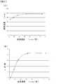
[工程−140]において、活性層を構成するInxGa(1-x)N層を結晶成長させるときのトリメチルインジウム(TMI)ガス供給量を0から60×10-6モル・分-1(1.4×10⁻⁶モル・cm-2・分-1)まで変化させたときの、InxGa(1-x)N層における「x」の値の変化を調べた結果を、図3の(A)に示す。結晶成長におけるその他の条件を、表5に「条件−A」として示す。図3の(A)の横軸の値の単位は「×10-6モル・分-1」であり、この値を「42cm2」で除すると、「×10-6モル・cm-2・分-1」を単位とした、下地1cm2当たり、1分当たりのIn系原料ガスの供給量(正規化された供給量)を得ることができる。図3の(A)から、1分当たりのIn系原料ガスの供給量が20×10-6モル・分-1以上の場合、即ち、下地1cm2当たり、1分当たりのIn系原料ガスの供給量が5×10⁻⁷モル・cm-2・分-1以上の場合、InxGa(1-x)N層における「x」の値が概ね安定することが判る。In [Step-140], the trimethylindium (TMI) gas supply amount for crystal growth of the Inx Ga(1-x) N layer constituting the active layer is 0 to 60 × 10−6 mol · min−1 ( FIG. 3 shows the result of examining the change in the value of “x” in the Inx Ga(1-x) N layer when it is changed to 1.4 × 10⁻⁶ mol · cm−2 · min−1 ). Of (A). Other conditions for crystal growth are shown in Table 5 as “Condition-A”. The unit of the value on the horizontal axis in FIG. 3A is “× 10−6 mol · min−1 ”, and when this value is divided by “42 cm2 ”, “× 10−6 mol · cm−2 · It is possible to obtain the supply amount (normalized supply amount) of In-based source gas per minute per 1 cm2 of the substrate in units of “minute−1 ”. From FIG. 3A, when the supply amount of In-based source gas per minute is 20 × 10−6 mol · min−1 or more, that is, the amount of In-based source gas per minute per 1 cm2 of the substrate. When the supply amount is 5 × 10⁻⁷ mol · cm−2 · min−1 or more, it can be seen that the value of “x” in the Inx Ga(1-x) N layer is almost stable.
また、活性層を結晶成長させるときの下地の温度と発光強度の関係を調べた。発光効率は、活性層を構成するInxGa(1-x)N層をKrレーザによって直接励起したときの発光強度(フォトルミネッセンス強度)を測定することで評価した。評価に使用した試料における活性層を構成するInxGa(1-x)N層の結晶成長条件は、表5に示した「条件−A」と同じであり、下地の温度と発光強度の測定結果を、図3の(B)に示す。図3の(B)から、下地の温度を高くすると、発光強度が増加することが判る。また、下地の温度が700゜C未満では、GaN系半導体発光素子の活性層が発光せず、下地の温度を上昇させると、発光効率が増加することが判る。Further, the relationship between the substrate temperature and the light emission intensity when the active layer was grown was examined. The luminous efficiency was evaluated by measuring the emission intensity (photoluminescence intensity) when the Inx Ga(1-x) N layer constituting the active layer was directly excited by a Kr laser. The crystal growth conditions of the Inx Ga(1-x) N layer constituting the active layer in the sample used for the evaluation are the same as “Condition-A” shown in Table 5, and measurement of the temperature and emission intensity of the substrate The results are shown in FIG. From FIG. 3B, it can be seen that the emission intensity increases when the temperature of the base is increased. In addition, it can be seen that when the substrate temperature is lower than 700 ° C., the active layer of the GaN-based semiconductor light-emitting element does not emit light, and the luminous efficiency increases when the substrate temperature is increased.
[表5]
更には、種々の試験により、活性層の成長速度を一定としたとき、下地の温度が10゜C上昇すると、活性層を構成するInxGa(1-x)Nにおける「x」の値が減少し、得られたLEDデバイスから成るGaN系半導体発光素子における発光波長が約40nm、短くなることが判明した。従って、活性層を構成するInxGa(1-x)N層の成長速度を0.3nm/秒以上、好ましくは0.6nm/秒以上とし、且つ、下地の温度を適切に選択、制御することで、活性層を構成するInxGa(1-x)N層における「x」の値を安定させ、且つ、所望の発光波長を有するGaN系半導体発光素子を得ることができる。尚、活性層をMOCVD法にて結晶成長させる際の雰囲気圧力(MOCVD装置内の圧力)を1×103Paから9×104Paまで、種々、変化させ、それ以外の結晶成長条件を上記の条件−4として、活性層を構成するInxGa(1-x)N層を結晶成長させたが、得られたInxGa(1-x)N層における「x」の値に、殆ど、変化はなかった。Furthermore, when the growth rate of the active layer is kept constant by various tests, the value of “x” in Inx Ga(1-x) N constituting the active layer increases when the substrate temperature rises by 10 ° C. It has been found that the emission wavelength in the GaN-based semiconductor light-emitting element comprising the obtained LED device is shortened by about 40 nm. Accordingly, the growth rate of the Inx Ga(1-x) N layer constituting the active layer is set to 0.3 nm / second or more, preferably 0.6 nm / second or more, and the base temperature is appropriately selected and controlled. This makes it possible to obtain a GaN-based semiconductor light-emitting element that stabilizes the value of “x” in the Inx Ga(1-x) N layer constituting the active layer and has a desired emission wavelength. In addition, the atmospheric pressure (pressure in the MOCVD apparatus) for crystal growth of the active layer by MOCVD is variously changed from 1 × 10³ Pa to 9 × 10⁴ Pa, and the other crystal growth conditions are as described above. As the condition-4, the Inx Ga(1-x) N layer constituting the active layer was crystal-grown, but the value of “x” in the obtained Inx Ga(1-x) N layer was almost equal to There was no change.
一般に、頂面がA面であるGaN系化合物半導体層の結晶成長はサファイア基板のR面上で行うことができるが、得られたGaN系化合物半導体層は結晶欠陥を極めて多く含んでおり、表面には凹凸が存在する。それ故、そのまま、このGaN系化合物半導体層上にGaN系化合物半導体から成る活性層等を形成すると、凹凸が更に拡大し、得られたGaN系半導体発光素子の発光も極めて弱くなる。 Generally, crystal growth of a GaN-based compound semiconductor layer whose top surface is an A-plane can be performed on the R-plane of a sapphire substrate, but the obtained GaN-based compound semiconductor layer contains a large number of crystal defects, and the surface There are irregularities. Therefore, when an active layer made of a GaN-based compound semiconductor is formed on the GaN-based compound semiconductor layer as it is, the unevenness is further expanded, and the light emission of the obtained GaN-based semiconductor light-emitting element becomes extremely weak.
実施例1のGaN系半導体発光素子の製造方法においては、先ず、シード層から、第1下地層をY方向に横方向エピタキシャル成長させるので、基本的には、結晶欠陥密度の極めて低い第1下地層を得ることができる。但し、シード層上に成長した第1下地層の部分における結晶欠陥密度は高い。それ故、シード層上に成長した第1下地層の結晶欠陥密度の高い部分の頂面をマスク層で覆った状態で、第1下地層の頂面上に第2下地層を形成する。その結果、得られた第2下地層における結晶欠陥密度は、全体として、極めて低くなる。 In the method for manufacturing a GaN-based semiconductor light-emitting device of Example 1, first, since the first underlayer is laterally epitaxially grown in the Y direction from the seed layer, basically, the first underlayer having an extremely low crystal defect density is used. Can be obtained. However, the crystal defect density in the portion of the first underlayer grown on the seed layer is high. Therefore, the second underlayer is formed on the top surface of the first underlayer in a state where the top surface of the portion of the first underlayer having a high crystal defect density grown on the seed layer is covered with the mask layer. As a result, the crystal defect density in the obtained second underlayer is extremely low as a whole.
しかも、こうして得られた第2下地層の頂面はA面であり、側面はC面等である。従って、下地に相当する第2下地層の上に順次形成される、第1GaN系化合物半導体層、活性層、第2GaN系化合物半導体層にあっても、これらの頂面はA面であり、側面(例えばC面)は界面に垂直な状態となる。従って、活性層にたとえピエゾ自発分極が生じた場合であっても、活性層の厚さ方向とは直角の方向にピエゾ自発分極が生じるので、発光波長にシフトが生じたり、発光効率の低下、動作電圧の上昇、輝度飽和といった現象が発生することを抑制することができる。 Moreover, the top surface of the second underlayer thus obtained is the A surface, and the side surface is the C surface. Therefore, even in the first GaN-based compound semiconductor layer, the active layer, and the second GaN-based compound semiconductor layer, which are sequentially formed on the second underlayer corresponding to the underlayer, these top surfaces are A-planes, side surfaces (For example, the C plane) is in a state perpendicular to the interface. Therefore, even if piezo spontaneous polarization occurs in the active layer, piezo spontaneous polarization occurs in a direction perpendicular to the thickness direction of the active layer, so that the emission wavelength shifts, the luminous efficiency decreases, Occurrence of phenomena such as an increase in operating voltage and saturation of luminance can be suppressed.
尚、実施例1の変形例として、マスク層13を形成しないGaN系半導体発光素子の製造方法を採用することもできる。この場合には、上述した[工程−110]の後、[工程−120]を実行することなく、直ちに、[工程−130]以降を実行すればよい。この場合にあっては、シード層11の上方に位置する第2下地層14の部分に結晶欠陥が生じる場合があるので、係る第2下地層14の部分の上方に相当する第2GaN系化合物半導体層の部分の上に、例えば、SiO2から成る被覆層を設け、第2導電型を有する第2GaN系化合物半導体層の係る部分の上には第2電極を形成しない構造とし、係る第2下地層14の部分の上方に位置する、第1導電型を有する第1GaN系化合物半導体層、活性層、第2導電型を有する第2GaN系化合物半導体層のそれぞれの部分に電流を流さない構成とすることが望ましい。As a modification of the first embodiment, a method for manufacturing a GaN-based semiconductor light-emitting element in which the
実施例2は、実施例1の変形である。実施例1にあっては、各第1下地層12の対向する側面12Bが相互に接触した時点で、第1下地層12の横方向エピタキシャル成長を中止する。ところで、GaN系化合物半導体結晶におけるc軸方向の熱膨張係数は、サファイア基板の熱膨張係数よりも極めて小さい。従って、温度の大きな変化に起因して、シード層11や第1下地層12がサファイア基板10から剥離する虞がある。 The second embodiment is a modification of the first embodiment. In Example 1, the lateral epitaxial growth of the
実施例2にあっては、実施例1の[工程−110]と同様の工程において、第1下地層12を、各シード層11からY方向に横方向エピタキシャル成長させ、各第1下地層12の対向する側面12Bが相互に接触する前に、横方向エピタキシャル成長を中止する。また、実施例1の[工程−130]と同様の工程において、第2下地層14をY方向に横方向エピタキシャル成長させると共に、第1下地層12の対向する側面12Bから第3下地層15をY方向に横方向エピタキシャル成長させる。これによって、実施例1の[工程−110]と同様の工程において、マスク層13を形成するためにサファイア基板10を降温したときに熱膨張係数の相違によって第1下地層12やシード層11がサファイア基板10から剥離することを、確実に防止することができる。 In Example 2, in the same process as [Step-110] of Example 1, the
以下、サファイア基板等の模式的な一部端面図である図4の(A)〜(D)を参照して、実施例2のGaN系半導体発光素子の製造方法を説明する。 Hereinafter, a method for manufacturing the GaN-based semiconductor light-emitting element of Example 2 will be described with reference to FIGS. 4A to 4D which are schematic partial end views of a sapphire substrate and the like.
[工程−200]
先ず、実施例1の[工程−100]と同様にして、サファイア基板10のR面上に、GaN系化合物半導体から成り、X方向に延びる帯状の離間したシード層11を複数形成する(図4の(A)参照)。[Step-200]
First, a plurality of strip-like seed layers 11 made of a GaN-based compound semiconductor and extending in the X direction are formed on the R surface of the
[工程−210]
次いで、頂面12AがA面であり、側面12BがC面である第1下地層12を、各シード層11の頂面からY方向に横方向エピタキシャル成長させる(図4の(B)参照)。実施例2にあっては、第1下地層12を、各シード層11からY方向に横方向エピタキシャル成長させ、各第1下地層12の対向する側面12Bが相互に接触する前に、横方向エピタキシャル成長を中止する。具体的には、実施例1の[工程−110]と同様の工程を実行する。但し、結晶成長の時間を、実施例1よりは短くする。[Step-210]
Next, the
[工程−220]
次いで、実施例1の[工程−120]と同様にして、シード層11の上方に位置する第1下地層12の頂面12Aの部分に、マスク層13を形成する(図4の(C)参照)。[Step-220]
Next, in the same manner as in [Step-120] in Example 1, a
[工程−230]
その後、実施例1の[工程−130]と同様にして、第2下地層14を第1下地層12の頂面12AからY方向に横方向エピタキシャル成長させると共に、第1下地層12の対向する側面12Bから第3下地層15をY方向に横方向エピタキシャル成長させる(図4の(D)参照)。[Step-230]
Thereafter, the second underlayer 14 is laterally epitaxially grown in the Y direction from the
こうして、第2下地層14から成り、無極性面である下地を得ることができる。 In this way, it is possible to obtain a base which is composed of the second base layer 14 and is a nonpolar surface.
[工程−240]
その後、実施例1の[工程−140]〜[工程−170]と同様の工程を実行することで、GaN系半導体発光素子を得ることができる。[Step-240]
Thereafter, the same steps as [Step-140] to [Step-170] in Example 1 are performed, whereby a GaN-based semiconductor light-emitting element can be obtained.
実施例2にあっては、[工程−210]において、第1下地層を、各シード層の頂面からY方向に横方向エピタキシャル成長させ、各第1下地層の対向する側面が相互に接触する前に、横方向エピタキシャル成長を中止する形態を採用するので、例えば、マスク層を形成するためにサファイア基板を降温したときに熱膨張係数の相違によってGaN系化合物半導体から成るシード層や第1下地層がサファイア基板から剥離することを、確実に防止することができる。 In Example 2, in [Step-210], the first underlayer is laterally epitaxially grown in the Y direction from the top surface of each seed layer, and the opposing side surfaces of each first underlayer are in contact with each other. Since a mode in which the lateral epitaxial growth is stopped before is adopted, for example, when a sapphire substrate is cooled to form a mask layer, a seed layer or a first underlayer made of a GaN-based compound semiconductor due to a difference in thermal expansion coefficient Can be reliably prevented from peeling from the sapphire substrate.
実施例3は実施例2の変形である。実施例3が実施例2と相違する主たる点は、第1下地層12を、各シード層11からY方向に横方向エピタキシャル成長させるときの結晶成長条件、特に、窒素源ガス(具体的には、アンモニアガス)の供給量を増加させた点にある。 The third embodiment is a modification of the second embodiment. The main difference between the third embodiment and the second embodiment is that crystal growth conditions when the
[工程−300]
先ず、実施例1の[工程−100]と同様にして、GaN系化合物半導体から成り、X方向に延びる帯状の離間したシード層11を複数形成する。尚、実施例3においては、
WS= 6μm
PS=24μm
とする。[Step-300]
First, similarly to [Step-100] of Example 1, a plurality of strip-like seed layers 11 made of a GaN-based compound semiconductor and extending in the X direction are formed. In Example 3,
WS = 6μm
PS = 24 μm
And
[工程−310]
次いで、頂面12AがA面であり、側面12BがC面である第1下地層12を、実施例2の[工程−210]と同様にして、各シード層11の頂面からY方向に横方向エピタキシャル成長させる。実施例3にあっても、第1下地層12を、各シード層11の頂面からY方向に横方向エピタキシャル成長させ、各第1下地層12の対向する側面12Bが相互に接触する前に、横方向エピタキシャル成長を中止する。具体的には、実施例1の[工程−110]と同様の工程を実行する。但し、結晶成長の時間を、実施例1よりは短くする。また、表1の結晶成長条件では、場合によっては、得られた第1下地層12に点欠陥が多く存在し、また、有機ガリウム源ガス中の炭素が第1下地層12に多く含まれ、黄色の発光が増えてしまう場合がある。それ故、実施例3にあっては、表1における窒素源ガス(具体的には、アンモニアガス)の供給量を1SLMから2SLMへと変更した。尚、実施例1に示した第1下地層12の結晶成長条件では、横方向成長速度が速く、窒素源ガス流量が少ないこともあり、第1下地層12が褐色に着色する場合があるが、実施例3の第1下地層12の結晶成長条件では、第1下地層12が着色せず、透明となる。しかも、窒素源ガス流量を2SLMとすることで、横方向成長速度が相対的に遅くなり、各第1下地層12の対向する側面12Bが相互に接触し難くなる傾向にある。[Step-310]
Next, in the same manner as in [Step-210] of Example 2, the
[工程−320]
次いで、実施例1の[工程−120]と同様にして、シード層11の上方に位置する第1下地層12の頂面12Aの部分に、マスク層13を形成する。尚、平面形状が帯状のマスク層13の幅WMを9μmとする。即ち、シード層11の射影像は、マスク層13の射影像に含まれ、WM/WS=1.5である。[Step-320]
Next, in the same manner as in [Step-120] of Example 1, a
[工程−330]
その後、実施例1の[工程−130]と同様にして、第2下地層14を第1下地層12の頂面12AからY方向に横方向エピタキシャル成長させると共に、第1下地層12の対向する側面12Bから第3下地層15をY方向に横方向エピタキシャル成長させる。[Step-330]
Thereafter, the second underlayer 14 is laterally epitaxially grown in the Y direction from the
こうして、第2下地層14から成り、無極性面である下地を得ることができる。 In this way, it is possible to obtain a base which is composed of the second base layer 14 and is a nonpolar surface.
[工程−340]
その後、実施例1の[工程−140]〜[工程−170]と同様の工程を実行することで、GaN系半導体発光素子を得ることができる。[Step-340]
Thereafter, the same steps as [Step-140] to [Step-170] in Example 1 are performed, whereby a GaN-based semiconductor light-emitting element can be obtained.
実施例4は、本発明の第2の構成に係るGaN系半導体発光素子の製造方法に関する。以下、実施例4のGaN系半導体発光素子の製造方法を説明する。 Example 4 relates to a method for manufacturing a GaN-based semiconductor light-emitting device according to the second configuration of the present invention. Hereinafter, a method for manufacturing the GaN-based semiconductor light-emitting device of Example 4 will be described.
[工程−400]
先ず、GaN基板をダイサーで切断することで、頂面がA面であるバルク状のGaN基板を準備し、次いで、例えばCMP法に基づきGaN基板の頂面を研磨することで、頂面がA面であり、しかも、平滑なバルク状のGaN基板を、下地として得ることができる。尚、GaN基板の表面に極性が反転している領域などがあれば、その部分を避けてGaN系半導体発光素子を製造することが望ましい。[Step-400]
First, a GaN substrate is cut with a dicer to prepare a bulk GaN substrate whose top surface is an A plane, and then the top surface of the GaN substrate is polished by, for example, a CMP method so that the top surface is A A smooth and bulky GaN substrate can be obtained as a base. It should be noted that it is desirable to manufacture a GaN-based semiconductor light-emitting element by avoiding the region where the polarity is reversed on the surface of the GaN substrate.
[工程−410]
そして、このGaN基板をMOCVD装置に搬入し、実施例1の[工程−140]と同様にして、第1導電型を有する第1GaN系化合物半導体層(具体的には、例えば、Siをドーピングした厚さ約1μmのGaN層)、InxGa(1-x)Nから成る活性層(具体的には、例えば、実施例1において説明した活性層と同じ構成、構造を有する)、第2導電型を有する第2GaN系化合物半導体層(具体的には、例えば、Mgをドーピングした厚さ5〜20nmのAlGaN層と、Mgをドーピングした厚さ100nmのGaN層)を、順次、MOCVD法にて、GaN基板の頂面(A面)上に結晶成長させる。[Step-410]
Then, this GaN substrate was carried into the MOCVD apparatus, and in the same manner as in [Step-140] in Example 1, the first GaN compound semiconductor layer having the first conductivity type (specifically, for example, doped with Si) A GaN layer having a thickness of about 1 μm), an active layer made of Inx Ga(1-x) N (specifically, for example, having the same configuration and structure as the active layer described in Example 1), second conductive A second GaN-based compound semiconductor layer having a type (specifically, for example, an AlGaN layer with a thickness of 5 to 20 nm doped with Mg and a GaN layer with a thickness of 100 nm doped with Mg) sequentially by MOCVD Then, crystals are grown on the top surface (A surface) of the GaN substrate.
[工程−420]
その後、実施例1の[工程−150]と同様にして、第2導電型(具体的には、p型)を有する第2GaN系化合物半導体層上に第2電極を形成する。第2電極は、Ni層/Ag層/Au層の積層構造を有し、真空蒸着法にて形成することができる。次に、GaN基板の裏面に、第1電極を形成する。第1電極は、Ti層/Au層の積層構造を有し、真空蒸着法にて形成することができる。更に、第1電極に接続されたITOから成る透明電極を形成する。その後、GaN基板を劈開することで、個々のGaN系半導体発光素子に分離する。こうして、GaN系半導体発光素子(LED)を得ることができる。そして、得られたLEDチップを、透明電極が上になるようにマウントし、配線を行い、樹脂モールドを行うことで、砲弾型のLEDデバイスから成るGaN系半導体発光素子を得ることができる。[Step-420]
Thereafter, in the same manner as in [Step-150] in Example 1, a second electrode is formed on the second GaN-based compound semiconductor layer having the second conductivity type (specifically, p-type). The second electrode has a stacked structure of Ni layer / Ag layer / Au layer and can be formed by a vacuum deposition method. Next, a first electrode is formed on the back surface of the GaN substrate. The first electrode has a laminated structure of Ti layer / Au layer and can be formed by a vacuum deposition method. Further, a transparent electrode made of ITO connected to the first electrode is formed. Thereafter, the GaN substrate is cleaved to be separated into individual GaN-based semiconductor light emitting devices. Thus, a GaN-based semiconductor light emitting device (LED) can be obtained. Then, the obtained LED chip is mounted so that the transparent electrode is on top, wiring is performed, and resin molding is performed, so that a GaN-based semiconductor light-emitting element composed of a bullet-type LED device can be obtained.
以上、本発明を好ましい実施例に基づき説明したが、本発明はこれらの実施例に限定されるものではない。実施例で説明した基板、活性層、各種GaN系化合物半導体層の種類、組成、膜厚、構成、構造等は例示であり、適宜変更することができる。また、実施例において説明した条件や各種数値、使用した材料等は例示であり、適宜変更することができる。 As mentioned above, although this invention was demonstrated based on the preferable Example, this invention is not limited to these Examples. The types, compositions, film thicknesses, configurations, structures, and the like of the substrate, active layer, and various GaN-based compound semiconductor layers described in the examples are examples and can be appropriately changed. In addition, the conditions, various numerical values, materials used, and the like described in the embodiments are examples, and can be appropriately changed.
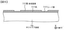
実施例1〜実施例3にあっては、GaN系化合物半導体から成るシード層11の形成方法を、サファイア基板10のR面上に、頂面がA面であるGaN系化合物半導体層を形成した後、リソグラフィ技術及びエッチング技術によってこのGaN系化合物半導体層をパターニングする方法としたが、シード層11の形成方法はこのような方法に限定するものではない。図5にサファイア基板10等の模式的な一部端面図を示すように、GaN系化合物半導体から成るシード層111は、サファイア基板10のR面上に、GaN系化合物半導体層111A(例えば、頂面がA面であるGaN層)を形成し、更に、その上に、非成長層(GaN系化合物半導体層がその上では成長しない層)111Bを形成した後、リソグラフィ技術及びエッチング技術によってこの非成長層111Bをパターニングし、X方向(より具体的には、<1−100>方向)に延びる帯状のGaN系化合物半導体層111Aを露出させることで、得ることもできる。 In Examples 1 to 3, the
10・・・サファイア基板、11・・・シード層、12・・・第1下地層、13・・・マスク層、14・・・第2下地層、15・・・第3下地層、111・・・シード層、111A・・・GaN系化合物半導体層、111B・・・非成長層
DESCRIPTION OF
Claims (10)
Translated fromJapanese(A)第1導電型を有し、頂面がA面である第1GaN系化合物半導体層、
(B)InxGa(1-x)Nから成り、頂面がA面である活性層、及び、
(C)第2導電型を有し、頂面がA面である第2GaN系化合物半導体層、
を、順次、結晶成長させる工程を具備したGaN系半導体発光素子の製造方法であって、
活性層を、成長速度0.3nm/秒以上にて結晶成長させることを特徴とするGaN系半導体発光素子の製造方法。On the base that is a nonpolar surface,
(A) a first GaN-based compound semiconductor layer having a first conductivity type and having a top surface that is an A-plane;
(B) an active layer made of Inx Ga(1-x) N, the top surface of which is an A plane, and
(C) a second GaN-based compound semiconductor layer having a second conductivity type and having a top surface that is an A-plane;
Is a method for manufacturing a GaN-based semiconductor light-emitting device comprising a step of sequentially growing crystals,
A method of manufacturing a GaN-based semiconductor light-emitting element, wherein the active layer is crystal-grown at a growth rate of 0.3 nm / second or more.
(b)GaN系化合物半導体から成り、頂面がA面である第1下地層を、各シード層からY方向に横方向エピタキシャル成長させ、次いで、
(c)シード層の上方に位置する第1下地層の頂面の部分に、マスク層を形成した後、
(d)第1下地層の頂面上及びマスク層上において、GaN系化合物半導体から成り、頂面がA面である第2下地層を第1下地層の頂面からY方向に横方向エピタキシャル成長させる、
各工程を更に具備し、
第2下地層が、前記下地層に相当することを特徴とする請求項8に記載のGaN系半導体発光素子の製造方法。(A) On the R surface of the sapphire substrate, a plurality of strip-like seed layers made of a GaN-based compound semiconductor and extending in the X direction are formed apart from each other,
(B) A first underlayer made of a GaN-based compound semiconductor and having a top surface that is an A plane is laterally epitaxially grown from each seed layer in the Y direction, and then
(C) After forming a mask layer on the top surface of the first underlayer located above the seed layer,
(D) On the top surface of the first underlayer and the mask layer, a second underlayer made of a GaN-based compound semiconductor and having a top surface of A-plane is laterally epitaxially grown in the Y direction from the top surface of the first underlayer. Let
Each step further comprises
The method for producing a GaN-based semiconductor light-emitting element according to claim 8, wherein the second underlayer corresponds to the underlayer.
2. The method for manufacturing a GaN-based semiconductor light-emitting element according to claim 1, wherein the base is composed of a GaN substrate having a top surface that is an A-plane.
Priority Applications (2)
| Application Number | Priority Date | Filing Date | Title |
|---|---|---|---|
| JP2005230415AJP2007048869A (en) | 2005-08-09 | 2005-08-09 | GaN-based semiconductor light emitting device manufacturing method |
| US11/463,233US7695991B2 (en) | 2005-08-09 | 2006-08-08 | Method for manufacturing GaN semiconductor light-emitting element |
Applications Claiming Priority (1)
| Application Number | Priority Date | Filing Date | Title |
|---|---|---|---|
| JP2005230415AJP2007048869A (en) | 2005-08-09 | 2005-08-09 | GaN-based semiconductor light emitting device manufacturing method |
Publications (1)
| Publication Number | Publication Date |
|---|---|
| JP2007048869Atrue JP2007048869A (en) | 2007-02-22 |
Family
ID=37743035
Family Applications (1)
| Application Number | Title | Priority Date | Filing Date |
|---|---|---|---|
| JP2005230415APendingJP2007048869A (en) | 2005-08-09 | 2005-08-09 | GaN-based semiconductor light emitting device manufacturing method |
Country Status (2)
| Country | Link |
|---|---|
| US (1) | US7695991B2 (en) |
| JP (1) | JP2007048869A (en) |
Cited By (5)
| Publication number | Priority date | Publication date | Assignee | Title |
|---|---|---|---|---|
| WO2009066464A1 (en)* | 2007-11-21 | 2009-05-28 | Mitsubishi Chemical Corporation | Nitride semiconductor and nitride semiconductor crystal growth method |
| WO2009066466A1 (en)* | 2007-11-21 | 2009-05-28 | Mitsubishi Chemical Corporation | Nitride semiconductor, nitride semiconductor crystal growth method, and nitride semiconductor light emitting element |
| JP2010056234A (en)* | 2008-08-27 | 2010-03-11 | Sumitomo Electric Ind Ltd | Method of manufacturing nitride semiconductor light-emitting element and method of manufacturing epitaxial wafer |
| JP2011023536A (en)* | 2009-07-15 | 2011-02-03 | Sumitomo Electric Ind Ltd | Gallium nitride-based semiconductor optical device, and method of fabricating the same |
| WO2015190000A1 (en)* | 2014-06-13 | 2015-12-17 | ウシオ電機株式会社 | Nitride semiconductor light emitting element |
Families Citing this family (15)
| Publication number | Priority date | Publication date | Assignee | Title |
|---|---|---|---|---|
| JP2008109066A (en)* | 2006-09-29 | 2008-05-08 | Rohm Co Ltd | Light emitting element |
| JP2008130655A (en)* | 2006-11-17 | 2008-06-05 | Toshiba Corp | Semiconductor element |
| WO2008141324A2 (en)* | 2007-05-14 | 2008-11-20 | S.O.I.Tec Silicon On Insulator Technologies | Methods for improving the quality of epitaxially-grown semiconductor materials |
| US8269251B2 (en)* | 2007-05-17 | 2012-09-18 | Mitsubishi Chemical Corporation | Method for producing group III nitride semiconductor crystal, group III nitride semiconductor substrate, and semiconductor light-emitting device |
| CN101730926B (en)* | 2007-07-26 | 2012-09-19 | 硅绝缘体技术有限公司 | Improved manufacturing method of epitaxial materials |
| US8178427B2 (en)* | 2009-03-31 | 2012-05-15 | Commissariat A. L'energie Atomique | Epitaxial methods for reducing surface dislocation density in semiconductor materials |
| WO2010140564A1 (en)* | 2009-06-01 | 2010-12-09 | 三菱化学株式会社 | Nitride semiconductor crystal and method for manufacturing same |
| US8105852B2 (en)* | 2010-01-15 | 2012-01-31 | Koninklijke Philips Electronics N.V. | Method of forming a composite substrate and growing a III-V light emitting device over the composite substrate |
| US9450143B2 (en)* | 2010-06-18 | 2016-09-20 | Soraa, Inc. | Gallium and nitrogen containing triangular or diamond-shaped configuration for optical devices |
| US8501597B2 (en)* | 2010-07-30 | 2013-08-06 | Academia Sinica | Method for fabricating group III-nitride semiconductor |
| JP5723341B2 (en)* | 2012-09-20 | 2015-05-27 | 株式会社東芝 | Manufacturing method of semiconductor device |
| DE102015217330A1 (en) | 2015-09-10 | 2017-03-16 | Technische Universität Berlin | Semiconductor device with active field shielded against internal fields |
| US11322652B2 (en)* | 2015-12-14 | 2022-05-03 | Ostendo Technologies, Inc. | Methods for producing composite GaN nanocolumns and light emitting structures made from the methods |
| MY190127A (en)* | 2016-10-31 | 2022-03-30 | Univ Malaya | Method for producing a non-polar a-plane gallium nitride (gan) thin film on an r-plane sapphire substrate |
| EP3373343B1 (en) | 2017-03-09 | 2021-09-15 | Technische Universität Berlin | Semiconductor device having an internal-field-guarded active region |
Family Cites Families (14)
| Publication number | Priority date | Publication date | Assignee | Title |
|---|---|---|---|---|
| JP3816176B2 (en) | 1996-02-23 | 2006-08-30 | 富士通株式会社 | Semiconductor light emitting device and optical semiconductor device |
| GB2327145A (en)* | 1997-07-10 | 1999-01-13 | Sharp Kk | Graded layers in an optoelectronic semiconductor device |
| JPH11340580A (en) | 1997-07-30 | 1999-12-10 | Fujitsu Ltd | Semiconductor laser, semiconductor light emitting device, and method of manufacturing the same |
| US6319742B1 (en)* | 1998-07-29 | 2001-11-20 | Sanyo Electric Co., Ltd. | Method of forming nitride based semiconductor layer |
| JP3375064B2 (en) | 1999-04-02 | 2003-02-10 | 日亜化学工業株式会社 | Method for growing nitride semiconductor |
| JP2001122693A (en)* | 1999-10-22 | 2001-05-08 | Nec Corp | Ground substrate for crystal growth and method of producing substrate using the same |
| JP4204163B2 (en) | 2000-02-03 | 2009-01-07 | 株式会社リコー | Manufacturing method of semiconductor substrate |
| JP3636976B2 (en)* | 2000-03-17 | 2005-04-06 | 日本電気株式会社 | Nitride semiconductor device and manufacturing method thereof |
| JP2002076522A (en)* | 2000-09-01 | 2002-03-15 | Nec Corp | Nitride semiconductor laser |
| JP3555657B2 (en) | 2000-09-25 | 2004-08-18 | 日亜化学工業株式会社 | Low defect nitride semiconductor substrate and method of manufacturing the same |
| JP3795765B2 (en) | 2001-04-06 | 2006-07-12 | ソニー株式会社 | Method for manufacturing compound semiconductor substrate |
| US6649942B2 (en)* | 2001-05-23 | 2003-11-18 | Sanyo Electric Co., Ltd. | Nitride-based semiconductor light-emitting device |
| US6683327B2 (en) | 2001-11-13 | 2004-01-27 | Lumileds Lighting U.S., Llc | Nucleation layer for improved light extraction from light emitting devices |
| US7485902B2 (en)* | 2002-09-18 | 2009-02-03 | Sanyo Electric Co., Ltd. | Nitride-based semiconductor light-emitting device |
- 2005
- 2005-08-09JPJP2005230415Apatent/JP2007048869A/enactivePending
- 2006
- 2006-08-08USUS11/463,233patent/US7695991B2/ennot_activeExpired - Fee Related
Cited By (15)
| Publication number | Priority date | Publication date | Assignee | Title |
|---|---|---|---|---|
| US8652948B2 (en) | 2007-11-21 | 2014-02-18 | Mitsubishi Chemical Corporation | Nitride semiconductor, nitride semiconductor crystal growth method, and nitride semiconductor light emitting element |
| JP2014033205A (en)* | 2007-11-21 | 2014-02-20 | Mitsubishi Chemicals Corp | Nitride semiconductor and crystal growth method for nitride semiconductor |
| JP2009147319A (en)* | 2007-11-21 | 2009-07-02 | Mitsubishi Chemicals Corp | Nitride semiconductor and nitride semiconductor crystal growth method |
| JP2009239250A (en)* | 2007-11-21 | 2009-10-15 | Mitsubishi Chemicals Corp | Nitride semiconductor, nitride semiconductor crystal growth method, and nitride semiconductor light-emitting element |
| EP2221856B1 (en)* | 2007-11-21 | 2020-09-09 | Mitsubishi Chemical Corporation | Nitride semiconductor, nitride semiconductor crystal growth method, and nitride semiconductor light emitting element |
| JP2016154237A (en)* | 2007-11-21 | 2016-08-25 | 三菱化学株式会社 | Crystal growth method and manufacturing method of light-emitting device |
| WO2009066466A1 (en)* | 2007-11-21 | 2009-05-28 | Mitsubishi Chemical Corporation | Nitride semiconductor, nitride semiconductor crystal growth method, and nitride semiconductor light emitting element |
| KR101502195B1 (en)* | 2007-11-21 | 2015-03-12 | 미쓰비시 가가꾸 가부시키가이샤 | Nitride semiconductor, nitride semiconductor crystal growth method, and nitride semiconductor light emitting element |
| WO2009066464A1 (en)* | 2007-11-21 | 2009-05-28 | Mitsubishi Chemical Corporation | Nitride semiconductor and nitride semiconductor crystal growth method |
| KR101495381B1 (en)* | 2007-11-21 | 2015-02-24 | 미쓰비시 가가꾸 가부시키가이샤 | Nitride semiconductor and nitride semiconductor crystal growth method |
| JP2014209664A (en)* | 2007-11-21 | 2014-11-06 | 三菱化学株式会社 | Crystal growth method of nitride semiconductor and nitride semiconductor light-emitting element |
| US9048100B2 (en) | 2007-11-21 | 2015-06-02 | Mitsubishi Chemical Corporation | Nitride semiconductor and nitride semiconductor crystal growth method |
| JP2010056234A (en)* | 2008-08-27 | 2010-03-11 | Sumitomo Electric Ind Ltd | Method of manufacturing nitride semiconductor light-emitting element and method of manufacturing epitaxial wafer |
| JP2011023536A (en)* | 2009-07-15 | 2011-02-03 | Sumitomo Electric Ind Ltd | Gallium nitride-based semiconductor optical device, and method of fabricating the same |
| WO2015190000A1 (en)* | 2014-06-13 | 2015-12-17 | ウシオ電機株式会社 | Nitride semiconductor light emitting element |
Also Published As
| Publication number | Publication date |
|---|---|
| US7695991B2 (en) | 2010-04-13 |
| US20070037308A1 (en) | 2007-02-15 |
Similar Documents
| Publication | Publication Date | Title |
|---|---|---|
| US7695991B2 (en) | Method for manufacturing GaN semiconductor light-emitting element | |
| JP4140606B2 (en) | GaN-based semiconductor light emitting device manufacturing method | |
| JP4978009B2 (en) | GaN-based semiconductor light-emitting device and manufacturing method thereof | |
| US7250320B2 (en) | Semiconductor light emitting element, manufacturing method thereof, integrated semiconductor light emitting device, manufacturing method thereof, image display device, manufacturing method thereof, illuminating device and manufacturing method thereof | |
| US8383493B2 (en) | Production of semiconductor devices | |
| US6153010A (en) | Method of growing nitride semiconductors, nitride semiconductor substrate and nitride semiconductor device | |
| JP2003218390A (en) | Semiconductor light emitting device and method of manufacturing the same | |
| JP2006347863A (en) | 3-5 nitride semiconductor multilayer substrate, 3-5 nitride semiconductor free-standing substrate manufacturing method, and semiconductor device | |
| US7452789B2 (en) | Method for forming underlayer composed of GaN-based compound semiconductor, GaN-based semiconductor light-emitting element, and method for manufacturing GaN-based semiconductor light-emitting element | |
| JPH11251632A (en) | Manufacture of gallium nitride semiconductor element | |
| JP4322187B2 (en) | Nitride semiconductor light emitting device | |
| JPH11274560A (en) | Semiconductor element and manufacture thereof | |
| JP2003031844A (en) | Method of manufacturing semiconductor light emitting device | |
| JP4652888B2 (en) | Method for manufacturing gallium nitride based semiconductor multilayer structure | |
| JP3884969B2 (en) | Semiconductor light emitting device and manufacturing method thereof | |
| JP2007131527A (en) | Nitride semiconductor substrate, nitride semiconductor laser device, method for manufacturing nitride semiconductor substrate, and method for manufacturing nitride semiconductor laser device | |
| JP2013035711A (en) | HEXAGONAL ROD-LIKE GaN-BASED SEMICONDUCTOR CRYSTAL AND METHOD FOR PRODUCING THE SAME | |
| JP2011134948A (en) | Method of growing nitride semiconductor | |
| JP2001345281A (en) | Method of manufacturing nitride-based iii group compound semiconductor and nitride-based iii group compound semiconductor element | |
| JP4857616B2 (en) | Method for forming GaN-based compound semiconductor layer and method for manufacturing GaN-based semiconductor light-emitting device | |
| JP5031674B2 (en) | Nitride semiconductor laser device and method for manufacturing nitride semiconductor laser device | |
| JP4806999B2 (en) | Method for forming an underlayer comprising a GaN-based compound semiconductor | |
| JP2003218468A (en) | Semiconductor laser element and manufacturing method therefor |
Legal Events
| Date | Code | Title | Description |
|---|---|---|---|
| A621 | Written request for application examination | Free format text:JAPANESE INTERMEDIATE CODE: A621 Effective date:20061206 | |
| A977 | Report on retrieval | Free format text:JAPANESE INTERMEDIATE CODE: A971007 Effective date:20090421 | |
| A131 | Notification of reasons for refusal | Free format text:JAPANESE INTERMEDIATE CODE: A131 Effective date:20090428 | |
| A02 | Decision of refusal | Free format text:JAPANESE INTERMEDIATE CODE: A02 Effective date:20090901 |