JP2007044863A - Conditioner for wafer polishing pad and its manufacturing method - Google Patents
Conditioner for wafer polishing pad and its manufacturing methodDownload PDFInfo
- Publication number
- JP2007044863A JP2007044863AJP2006038891AJP2006038891AJP2007044863AJP 2007044863 AJP2007044863 AJP 2007044863AJP 2006038891 AJP2006038891 AJP 2006038891AJP 2006038891 AJP2006038891 AJP 2006038891AJP 2007044863 AJP2007044863 AJP 2007044863A
- Authority
- JP
- Japan
- Prior art keywords
- polishing pad
- grooves
- wafer
- conditioner
- conditioner used
- Prior art date
- Legal status (The legal status is an assumption and is not a legal conclusion. Google has not performed a legal analysis and makes no representation as to the accuracy of the status listed.)
- Pending
Links
- 238000005498polishingMethods0.000titleclaimsabstractdescription53
- 238000004519manufacturing processMethods0.000titleclaimsabstractdescription28
- 239000006061abrasive grainSubstances0.000claimsabstractdescription58
- 239000000758substrateSubstances0.000claimsabstractdescription29
- 238000000034methodMethods0.000claimsdescription32
- 239000011230binding agentSubstances0.000claimsdescription14
- 238000005219brazingMethods0.000claimsdescription13
- 230000001050lubricating effectEffects0.000claimsdescription10
- 229910003481amorphous carbonInorganic materials0.000claimsdescription6
- 239000011248coating agentSubstances0.000claimsdescription6
- 238000000576coating methodMethods0.000claimsdescription6
- 229920000052poly(p-xylylene)Polymers0.000claimsdescription6
- 230000008439repair processEffects0.000claimsdescription3
- 238000005323electroformingMethods0.000claimsdescription2
- 238000007670refiningMethods0.000claims5
- 238000005530etchingMethods0.000claims1
- 239000000314lubricantSubstances0.000claims1
- 239000007767bonding agentSubstances0.000abstract2
- 239000000463materialSubstances0.000description17
- 230000008569processEffects0.000description11
- 238000005520cutting processMethods0.000description9
- 239000002699waste materialSubstances0.000description8
- OKTJSMMVPCPJKN-UHFFFAOYSA-NCarbonChemical compound[C]OKTJSMMVPCPJKN-UHFFFAOYSA-N0.000description6
- 229910045601alloyInorganic materials0.000description6
- 239000000956alloySubstances0.000description6
- 229910052799carbonInorganic materials0.000description6
- 229910003460diamondInorganic materials0.000description6
- 239000010432diamondSubstances0.000description6
- 229920002120photoresistant polymerPolymers0.000description6
- 238000004070electrodepositionMethods0.000description5
- 239000007788liquidSubstances0.000description5
- 230000007547defectEffects0.000description3
- 238000009826distributionMethods0.000description3
- 238000005461lubricationMethods0.000description3
- 229910052582BNInorganic materials0.000description2
- PZNSFCLAULLKQX-UHFFFAOYSA-NBoron nitrideChemical compoundN#BPZNSFCLAULLKQX-UHFFFAOYSA-N0.000description2
- XUIMIQQOPSSXEZ-UHFFFAOYSA-NSiliconChemical compound[Si]XUIMIQQOPSSXEZ-UHFFFAOYSA-N0.000description2
- 238000009825accumulationMethods0.000description2
- 239000003929acidic solutionSubstances0.000description2
- 239000012670alkaline solutionSubstances0.000description2
- 239000013078crystalSubstances0.000description2
- 238000005516engineering processMethods0.000description2
- 239000002184metalSubstances0.000description2
- 229910052751metalInorganic materials0.000description2
- 238000005240physical vapour depositionMethods0.000description2
- 239000004065semiconductorSubstances0.000description2
- 229910052710siliconInorganic materials0.000description2
- 239000010703siliconSubstances0.000description2
- 239000000126substanceSubstances0.000description2
- 238000001039wet etchingMethods0.000description2
- RYGMFSIKBFXOCR-UHFFFAOYSA-NCopperChemical compound[Cu]RYGMFSIKBFXOCR-UHFFFAOYSA-N0.000description1
- 230000002378acidificating effectEffects0.000description1
- 239000000919ceramicSubstances0.000description1
- 230000008859changeEffects0.000description1
- 229910052802copperInorganic materials0.000description1
- 239000010949copperSubstances0.000description1
- 230000007423decreaseEffects0.000description1
- 238000010586diagramMethods0.000description1
- 239000003989dielectric materialSubstances0.000description1
- 238000005553drillingMethods0.000description1
- 230000000694effectsEffects0.000description1
- 238000009499grossingMethods0.000description1
- 230000006872improvementEffects0.000description1
- 238000012423maintenanceMethods0.000description1
- 239000007769metal materialSubstances0.000description1
- 230000004048modificationEffects0.000description1
- 238000012986modificationMethods0.000description1
- 229920005749polyurethane resinPolymers0.000description1
- 239000010935stainless steelSubstances0.000description1
- 229910001220stainless steelInorganic materials0.000description1
- 230000003746surface roughnessEffects0.000description1
- 230000009466transformationEffects0.000description1
- WFKWXMTUELFFGS-UHFFFAOYSA-NtungstenChemical compound[W]WFKWXMTUELFFGS-UHFFFAOYSA-N0.000description1
- 229910052721tungstenInorganic materials0.000description1
- 239000010937tungstenSubstances0.000description1
- XLYOFNOQVPJJNP-UHFFFAOYSA-NwaterSubstancesOXLYOFNOQVPJJNP-UHFFFAOYSA-N0.000description1
Images


Classifications
- B—PERFORMING OPERATIONS; TRANSPORTING
- B24—GRINDING; POLISHING
- B24B—MACHINES, DEVICES, OR PROCESSES FOR GRINDING OR POLISHING; DRESSING OR CONDITIONING OF ABRADING SURFACES; FEEDING OF GRINDING, POLISHING, OR LAPPING AGENTS
- B24B53/00—Devices or means for dressing or conditioning abrasive surfaces
- B24B53/017—Devices or means for dressing, cleaning or otherwise conditioning lapping tools
- B—PERFORMING OPERATIONS; TRANSPORTING
- B24—GRINDING; POLISHING
- B24D—TOOLS FOR GRINDING, BUFFING OR SHARPENING
- B24D18/00—Manufacture of grinding tools or other grinding devices, e.g. wheels, not otherwise provided for
- B24D18/0027—Manufacture of grinding tools or other grinding devices, e.g. wheels, not otherwise provided for by impregnation
Landscapes
- Engineering & Computer Science (AREA)
- Mechanical Engineering (AREA)
- Manufacturing & Machinery (AREA)
- Grinding-Machine Dressing And Accessory Apparatuses (AREA)
- Finish Polishing, Edge Sharpening, And Grinding By Specific Grinding Devices (AREA)
- Polishing Bodies And Polishing Tools (AREA)
- Mechanical Treatment Of Semiconductor (AREA)
Abstract
Description
Translated fromJapanese本発明はウェハ研磨パッドのコンディショナ及びその製造方法に関し、特に、砥粒が均等にコンディショナに分布し、且つ、基板に強固に固着しているウェハ研磨パッドのコンディショナ及びその製造方法に関する。 The present invention relates to a wafer polishing pad conditioner and a method for manufacturing the same, and more particularly to a wafer polishing pad conditioner in which abrasive grains are evenly distributed in the conditioner and firmly fixed to a substrate and a method for manufacturing the same.
現在の半導体製造プロセスでは、技術の進歩に伴い、チップの線幅と面積が小型化し、導線の密集度も高まり、且つ、堆積する層もますます増えている。このため、チップ表面の平坦化の重要性が高まっているが、目下、全面的に平坦化したウェハを提供できる唯一の技術は化学的機械研磨(Chemical Mechanical Polishing;CMP)だけである。 In the current semiconductor manufacturing process, with the advancement of technology, the line width and area of a chip are reduced, the density of conductive wires is increased, and the number of deposited layers is increasing. For this reason, although the importance of planarizing the chip surface is increasing, at present, the only technique that can provide a completely planarized wafer is chemical mechanical polishing (CMP).
CMPプロセスにおいて、シリコンウェハは回転、或いは移動する研磨ヘッドによって回転する研磨パッドに押し付けられている。研磨パッド上には研磨液が注入されており、研磨液は通常、細かい砥粒の他に、研磨される材質によって調節される酸性もしくはアルカリ性の溶液が含まれている。例えば、誘電物質は通常酸化物であるが、この場合、研磨液として通常アルカリ性溶液を選択する。また、研磨金属材料がタングステンや銅であった場合、研磨液として通常酸性溶液を選択する。研磨パッドの材料は一般的にポリウレタン樹脂(Polyurethane resin)であり、且つ、研磨パッドは表面が粗く、穴があるため、CMPプロセスの際にシリコンウェハ研磨で生じる切削屑の殆どは水によって流されるが、一部の切削屑は次第に研磨パッドの孔に堆積してしまう。このため、研磨パッドの表面の粗さが徐々になくなり、研磨の速度を下げ、CMPプロセスを不安定にし、且つ研磨パッドの消耗を早めてしまう。 In the CMP process, a silicon wafer is pressed against a rotating polishing pad by a rotating or moving polishing head. A polishing liquid is poured onto the polishing pad, and the polishing liquid usually contains an acidic or alkaline solution adjusted in accordance with the material to be polished, in addition to fine abrasive grains. For example, the dielectric material is usually an oxide. In this case, an alkaline solution is usually selected as the polishing liquid. When the polishing metal material is tungsten or copper, an acidic solution is usually selected as the polishing liquid. The material of the polishing pad is generally a polyurethane resin, and since the polishing pad has a rough surface and a hole, most of the cutting waste generated by polishing the silicon wafer during the CMP process is washed away by water. However, some of the cutting waste gradually accumulates in the holes of the polishing pad. For this reason, the surface roughness of the polishing pad gradually disappears, the polishing speed is lowered, the CMP process becomes unstable, and the polishing pad is consumed quickly.
よって、コンディショナが必要とされる。コンディショナは研磨パッド表面に溜まった切削屑を除去し、研磨パッドを活性化させ、プロセスを安定にするほか、研磨液を均一に研磨パッドに分布させることができるので、プロセスをさらに安定にする。 Therefore, a conditioner is required. The conditioner removes cutting chips accumulated on the surface of the polishing pad, activates the polishing pad, stabilizes the process, and evenly distributes the polishing liquid to the polishing pad, making the process even more stable .
従来のコンディショナには、電着コンディショナと合金ブレージングコンディショナの二種類がよく見られる。電着コンディショナの砥粒は電着によって基板上に固着されるが、この種の物理的固着方法は固着力が優れず、砥粒が脱落してウェハを傷つけ易い。また、電着層が砥粒のほとんどを覆わなければ砥粒を固定できないため、砥粒の突出高度が限られ、有効に研磨パッドを修整できず、切削屑も詰まりやすい。よって、目下のCMPプロセスにおいて電着コンディショナはあまり使用されない。一方、合金ブレージングコンディショナでは、砥粒は合金ブレージングの方法で基板に固着されており、このような化学的固着方法は固着力が比較的よく、砥粒が脱落する状況は大幅に改善される。しかし、問題点として、基板上の砥粒の分布が、砥粒どうしの間隔にしろ、砥粒の位置する高さにしろ不均一になることがあり、そのため砥粒が不均一に研磨パッドに力を与え、より大きな力を受けた砥粒が丸ごと脱落したり、砥粒の角が部分的に破砕したりして、ウェハにスクラッチ傷を与えてしまう。更には、砥粒が分布する間隔が近すぎても、切削屑が堆積し易く、コンディショナの効率が下がり、切削屑の堆積が多すぎて脱落すると、ウェハを傷つけ易い。よって、上述の問題を改善した各種合金ブレージングコンディショナが既に提示されている。 Two types of conventional conditioners are commonly found: electrodeposition conditioners and alloy brazing conditioners. Although the abrasive grains of the electrodeposition conditioner are fixed on the substrate by electrodeposition, this kind of physical fixing method does not have excellent fixing force, and the abrasive grains fall off and easily damage the wafer. In addition, since the abrasive grains cannot be fixed unless the electrodeposition layer covers most of the abrasive grains, the protruding height of the abrasive grains is limited, the polishing pad cannot be effectively repaired, and the cutting waste tends to be clogged. Therefore, electrodeposition conditioners are not often used in the current CMP process. On the other hand, in the alloy brazing conditioner, the abrasive grains are fixed to the substrate by the alloy brazing method. Such a chemical fixing method has a relatively good fixing force, and the situation where the abrasive grains fall off is greatly improved. . However, the problem is that the distribution of the abrasive grains on the substrate may be non-uniform regardless of the distance between the abrasive grains, even at the height at which the abrasive grains are located. The abrasive grains that have been applied with a greater force drop off, or the corners of the abrasive grains are partially crushed, and the wafer is scratched. Furthermore, even if the interval at which the abrasive grains are distributed is too close, cutting waste tends to accumulate, the conditioner efficiency decreases, and if there is too much accumulation of cutting waste and falls off, the wafer is likely to be damaged. Therefore, various alloy brazing conditioners that have improved the above-mentioned problems have already been presented.
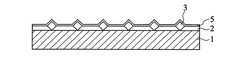
ここで、米国特許第6368198号公報には、コンディショナ及びその製造方法が開示されている。図1に示すように、ろう材層2により砥粒3を基板1に固着させている。砥粒3が比較的均一に分布できる理由は、ブレージングの前に、穴のあるパターンプレート(図示せず)を用いて砥粒3をろう材層2に導入して、位置決めをしているためである。また、物理気相成長法(Physical Vapor Deposition;PVD)によって、その上に酸性やアルカリ性に耐えるダイヤモンドライクカーボンDLC(Diamond-Like Carbon)膜5を形成する。しかしながら、この従来のコンディショナにおいても、砥粒分布の均一性にはまだ改善の余地があり、また、砥粒が脱落する状況も依然生じている。よって、いかに砥粒の分布が均等で、且つ強固に基板に固着しているコンディショナを提供するかが、目下のところ、半導体製造技術の急を要する課題である。
よって、本発明の目的は、均一にウェハ研磨パッドを修整できるコンディショナ及びその製造方法を提供することである。 Accordingly, an object of the present invention is to provide a conditioner capable of uniformly modifying a wafer polishing pad and a method for manufacturing the same.
本発明のもう一つの目的は、砥粒が強固に基板上に固着した、ウェハ研磨パッドを修整するコンディショナ及びその製造方法を提供することである。 Another object of the present invention is to provide a conditioner for repairing a wafer polishing pad in which abrasive grains are firmly fixed on a substrate, and a method for manufacturing the same.
本発明において、砥粒は、天然ダイヤモンド、人工単結晶ダイヤモンド、多結晶ダイヤモンド(PCD)、立方晶窒化ホウ素(CBN)、多結晶立方晶窒化ホウ素(PcBN)などを含む、あらゆる超高硬度の結晶体を指す。 In the present invention, the abrasive grains are all ultra-high hardness crystals including natural diamond, artificial single crystal diamond, polycrystalline diamond (PCD), cubic boron nitride (CBN), polycrystalline cubic boron nitride (PcBN) and the like. Refers to the body.
本発明において、基板は各種材料によって構成される底材、例えば、金属、合金、セラミックスなどを指す。 In the present invention, the substrate refers to a bottom material composed of various materials, for example, a metal, an alloy, a ceramic, and the like.
本発明において、溝は砥粒の収納と固着に用いられ、溝の形状は、例えば半円球状、碗状、筒状、錐状など各形状でもよい。 In the present invention, the groove is used for storing and fixing the abrasive grains, and the shape of the groove may be, for example, a semispherical shape, a bowl shape, a cylindrical shape, or a cone shape.
本発明において、結合材は例えば金属、合金などの基板と砥粒を固着する任意の材料である。 In the present invention, the binding material is an arbitrary material for fixing the abrasive grains to the substrate such as metal or alloy.
本発明が提供するウェハ研磨パッドを修整するコンディショナは、上表面に複数の溝を有する基板と、前記複数の溝に充填される結合材と、前記結合材によって前記複数の溝内に固着された複数の砥粒と、を有する。このうち複数の溝は規則的に配列されていることが望ましく、更に、溝の寸法(口径幅)は一つの溝に一つの砥粒のみが収納できる大きさが望ましく、また、前記複数の溝の形は碗状が望ましい。前記結合材はブレージングの方法によって前記複数の砥粒を前記複数の溝内に固着する。 A conditioner for repairing a wafer polishing pad provided by the present invention is fixed in a plurality of grooves by a substrate having a plurality of grooves on an upper surface, a bonding material filled in the plurality of grooves, and the bonding material. A plurality of abrasive grains. Of these, it is desirable that the plurality of grooves are regularly arranged, and further, the dimension (caliber width) of the grooves is preferably large enough to accommodate only one abrasive grain in one groove, and the plurality of grooves The shape of 碗 is desirable. The binding material fixes the plurality of abrasive grains in the plurality of grooves by a brazing method.
上述のウェハの研磨パッドを修整するコンディショナは、さらに、パリレン(Parylene)、アモルファスカーボン・コーティング(WC/C)、ダイヤモンド膜、或いは、ダイヤモンドライクカーボン(DLC)膜である潤滑層を有していることが望ましい。前記潤滑層は、切削屑排出の速度を速め、切削屑の堆積を減少し、且つ修整時間を減らすことができる。 The above-described conditioner for modifying the polishing pad of the wafer further includes a lubricating layer which is a Parylene, an amorphous carbon coating (WC / C), a diamond film, or a diamond-like carbon (DLC) film. It is desirable. The lubricating layer can increase the speed of cutting waste discharge, reduce the accumulation of cutting waste, and reduce the modification time.
本発明は更にウェハの研磨パッドを修整するコンディショナの製造方法を提供する。該方法は、基板を提供するステップと、基板の上表面に複数の溝を形成するステップと、結合材を前記複数の溝に充填するステップと、複数の砥粒を結合材内に設置(配置)し、その結合材によって複数の砥粒と基板を強固に固着させるステップを含む。 The present invention further provides a method of manufacturing a conditioner for modifying a wafer polishing pad. The method includes the steps of providing a substrate, forming a plurality of grooves in an upper surface of the substrate, filling the plurality of grooves with a bonding material, and installing (arranging) a plurality of abrasive grains in the bonding material. And a step of firmly fixing the plurality of abrasive grains and the substrate with the binder.
前記複数の溝は規則的に配列されていることが望ましい。更に、複数の溝の各寸法は一つの溝に一つの砥粒のみが収納できる大きさが望ましく、また、前記複数の溝の形状は碗状が望ましい。さらに、前記結合材はブレージングの方法によって前記複数の砥粒を前記複数の溝内に固着するものであると好ましい。 It is desirable that the plurality of grooves are regularly arranged. Furthermore, each dimension of the plurality of grooves is preferably large enough to accommodate only one abrasive grain in one groove, and the shape of the plurality of grooves is preferably bowl-shaped. Furthermore, it is preferable that the binding material fix the plurality of abrasive grains in the plurality of grooves by a brazing method.
上記のコンディショナの製造方法は、さらに、前記基板と、前記結合材と、前記複数の砥粒と、の上、すなわち、前記複数の砥粒と前記基板とが前記結合材により固着されたものの上(上面)に潤滑層を形成するステップを含むと好適である。また、潤滑層としては、パリレン(Parylene)、アモルファスカーボン・コーティング(WC/C)、ダイヤモンド膜、或いは、ダイヤモンドライクカーボン(DLC)膜などが挙げられる。 The above-described conditioner manufacturing method is further provided on the substrate, the binder, and the plurality of abrasive grains, that is, the plurality of abrasive grains and the substrate are fixed by the binder. It is preferable to include a step of forming a lubricating layer on the upper surface (upper surface). Examples of the lubricating layer include parylene, amorphous carbon coating (WC / C), diamond film, and diamond-like carbon (DLC) film.
本発明によれば、コンディショナがウェハの研磨パッドを修整する効率と均一性を高めることができ、研磨パッドの寿命を向上させることができる。さらに、本発明はCMPプロセスの安定性を高めることができ、修整の時間を減らし、設備のメンテナンスに必要な回数と時間を減らすことができ、ウェハが損傷するという欠陥を減少できるため、ウェハの歩留まりと産量を上げることができる。 According to the present invention, the efficiency and uniformity of the conditioner modifying the polishing pad of the wafer can be increased, and the life of the polishing pad can be improved. In addition, the present invention can increase the stability of the CMP process, reduce the time required for repairs, reduce the number of times and time required for equipment maintenance, and reduce defects such as wafer damage. Yield and production can be increased.
本発明の実施形態について図面を参照にしながら説明する。図中、同一の要素には同一の符号を付し、重複する説明を省略する。また、後述の実施形態は本発明の内容を簡単に説明するためであり、実施形態において特に制限を定義している場合を除き、本発明はそれらに狭義的に制限されるものではない。 Embodiments of the present invention will be described with reference to the drawings. In the figure, the same elements are denoted by the same reference numerals, and redundant description is omitted. In addition, the embodiments described below are for the purpose of briefly explaining the contents of the present invention, and the present invention is not limited to them in a narrow sense unless the embodiment particularly defines a limitation.
[第1実施形態]
図2は、本発明によるコンディショナの第1実施形態を示す側面図である。図2において、結合材12は、砥粒13を、基板11上にある複数の底部が平らな碗状の溝14に固着させている。また、第1実施形態において、基板11はステンレス鋼SUS316で形成されており、砥粒の大きさは100μm〜250μm、より好ましくは130μm〜200μmであり、溝14の深さは一例として50μmであるが、溝14の深さは、砥粒の大きさと砥粒を露出させる程度によって適宜調整できる。さらに、溝14は、その口径(幅寸法)が、砥粒一つだけを収容できるように設けられており、砥粒を溝14の位置に従って均一に分布させる。また、溝14は底部が平らな碗状であり、これにより、構造上しっかりと強固に砥粒13を固着して砥粒を脱落し難くする。[First Embodiment]
FIG. 2 is a side view showing a first embodiment of a conditioner according to the present invention. In FIG. 2, the bonding
[第2実施形態]
図3は、本発明によるコンディショナの第2実施形態を示す側面図である。第2実施形態のコンディショナは、実施例1のコンディショナ上に更に潤滑層15を沈積(形成)させたものである。潤滑層15は、好ましくは、ダイヤモンド膜、ダイヤモンドライクカーボン(DLC)、パリレン(Parylene)、アモルファスカーボン・コーティング(WC/C)などから形成されており、より好ましくは、パリレン(Parylene)、アモルファスカーボン・コーティング(WC/C)などで形成されている。潤滑層15は、酸性やアルカリ性への耐久性により、異なるプロセス条件に適応できるだけでなく、コンディショナの表面に生じた欠陥を補填して、コンディショナの表面をより平滑にし、切削屑を排除する速度を向上させることができる。このようにして、従来問題であったCMPプロセスを行う時に表面の欠陥により圧力が不均一にかかるため砥粒が脱落したり、砥粒の角が一部砕けたりといった現象を減らすことができ、ウェハに損傷を与えることを防止できる。[Second Embodiment]
FIG. 3 is a side view showing a second embodiment of the conditioner according to the present invention. In the conditioner of the second embodiment, the
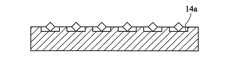
[第3実施形態]
図4は、本発明によるコンディショナの第3実施形態を示す側面図である。第3実施形態のコンディショナは、第1実施形態のコンディショナの底部が平らな碗状の溝14に替えて、筒状の溝14aを有するものである。[Third Embodiment]
FIG. 4 is a side view showing a third embodiment of the conditioner according to the present invention. The conditioner of the third embodiment has a
[第4実施形態]
図5は、本発明によるコンディショナの第4実施形態を示す側面図である。第4実施形態のコンディショナは、第1実施形態のコンディショナの底部が平らな碗状の溝14に替えて、錐状の溝14bを有するものである。[Fourth Embodiment]
FIG. 5 is a side view showing a fourth embodiment of the conditioner according to the present invention. The conditioner of the fourth embodiment has a
なお、本発明における「溝」の形は、上述の各実施形態に制限されず、この他の形状の溝を用いても本発明の効果を達成できる。 In addition, the shape of the “groove” in the present invention is not limited to the above-described embodiments, and the effect of the present invention can be achieved even if grooves having other shapes are used.
[製造方法の実施形態]
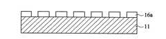
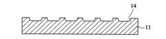
図6A〜図6Eは、それぞれ、本発明によるコンディショナの製造方法の好適な一実施形態により、コンディショナを製造している状態を示す工程図である。図6Aが示すように、まず、基板11を提供し、その上にフォトレジスト層16を形成し、予め定義してあるパターン(図示せず)でフォトレジスト層16を露光、現像し、図6Bに示すような、パターンを有するフォトレジスト層16aを得る。次に、図6Cに示すように、ウェットエッチングによって基板11上に碗状の溝14を形成し、フォトレジスト層16aを除去する。そして、図6Dに示すように、溝14に結合材12を充填し、最後に、図6Eが示すように、砥粒13を結合材12内に設置(配置)し、真空ブレージングを行って結合材12を砥粒13と基板11に強固に固着させる。[Embodiment of Manufacturing Method]
FIG. 6A to FIG. 6E are process diagrams showing a state in which a conditioner is manufactured according to a preferred embodiment of a method for manufacturing a conditioner according to the present invention. As shown in FIG. 6A, first, a
なお、本発明のコンディショナの製造方法において、上記溝を形成する方法はウェットエッチングに制限されず、レーザードリル(Laser Drill)や電鋳(Galvono)、またはその他の方法で溝を形成してもよい。 In the conditioner manufacturing method of the present invention, the method of forming the groove is not limited to wet etching, and the groove may be formed by laser drilling, electroforming (Galvono), or other methods. Good.
以上、本発明の実施形態について図面を参照して詳述したが、具体的な構成は、これらの実施形態に限られるものではなく、本発明の要旨を逸脱しない範囲において種々の変形が可能であり、かかる範囲内で設計変更等があっても、それは本発明に含まれる。 As mentioned above, although embodiment of this invention was explained in full detail with reference to drawings, a concrete structure is not restricted to these embodiment, A various deformation | transformation is possible in the range which does not deviate from the summary of this invention. Even if there is a design change or the like within such a range, it is included in the present invention.
本発明によるコンディショナ及びその製造方法は、ウェハ等の基板の研磨ひいては該基板を用いた種々のデバイス、及びその製造等に広く用いることができる。 The conditioner and the manufacturing method thereof according to the present invention can be widely used for polishing a substrate such as a wafer, and various devices using the substrate, manufacturing the same, and the like.
1 基板
2 ろう材層
3 砥粒
5 ダイヤモンドライクカーボン膜
11 基板
12 結合材
13 砥粒
14 溝
14a 溝
14b 溝
15 潤滑層
16 フォトレジスト層
16a パターンを有するフォトレジスト層1 Board
2 Brazing material layer
3 Abrasive grains
5 Diamond-like carbon film
11 Board
12 Binder
13 Abrasive grain
14 groove
14a groove
14b groove
15 Lubrication layer
16 Photoresist layer
Photoresist layer with 16a pattern
Claims (17)
Translated fromJapanese上表面に複数の溝を有する基板と、
前記複数の溝に充填される結合材と、
前記結合材により前記複数の溝に固着された複数の砥粒と、
を有することを特徴とするウェハの研磨パッドの修整に用いられるコンディショナ。A conditioner used to modify a polishing pad on a wafer,
A substrate having a plurality of grooves on the upper surface;
A binder filling the plurality of grooves;
A plurality of abrasive grains fixed to the plurality of grooves by the binder;
A conditioner used for refining a polishing pad of a wafer, characterized by comprising:
ことを特徴とする請求項1に記載のウェハの研磨パッドの修整に用いられるコンディショナ。The plurality of grooves are regularly arranged;
2. A conditioner used for repairing a polishing pad of a wafer according to claim 1.
ことを特徴とする請求項1又は2に記載のウェハの研磨パッドの修整に用いられるコンディショナ。Each dimension of the plurality of grooves is a size that can accommodate only one abrasive grain.
The conditioner used for the correction of the polishing pad of the wafer of Claim 1 or 2 characterized by the above-mentioned.
ことを特徴とする請求項1〜3のいずれか1項に記載のウェハの研磨パッドの修整に用いられるコンディショナ。The plurality of grooves are bowl-shaped, conical, or cylindrical with a flat bottom.
The conditioner used for the correction | amendment of the polishing pad of the wafer of any one of Claims 1-3 characterized by the above-mentioned.
ことを特徴とする請求項1〜4のいずれか1項に記載のウェハの研磨パッドの修整に用いられるコンディショナ。The binder is to fix the plurality of abrasive grains and the plurality of grooves by a brazing method.
The conditioner used for the correction | amendment of the polishing pad of the wafer of any one of Claims 1-4 characterized by the above-mentioned.
ことを特徴とする請求項1〜5のいずれか1項に記載のウェハの研磨パッドの修整に用いられるコンディショナ。A lubricant layer;
The conditioner used for the correction | amendment of the polishing pad of the wafer of any one of Claims 1-5 characterized by the above-mentioned.
ことを特徴とする請求項6に記載のウェハの研磨パッドの修整に用いられるコンディショナ。The lubricating layer is parylene;
A conditioner used for refining a polishing pad for a wafer according to claim 6.
ことを特徴とする請求項6に記載のウェハの研磨パッドの修整に用いられるコンディショナ。The lubricating layer is an amorphous carbon coating;
A conditioner used for refining a polishing pad for a wafer according to claim 6.
基板を提供するステップと、
前記基板の上表面に複数の溝を形成するステップと、
結合材を前記複数の溝に充填するステップと、
複数の砥粒を前記結合材内に設置するステップと、
前記結合材により前記複数の砥粒と前記基板とを固着させるステップと、
を有することを特徴とするウェハの研磨パッドの修整に用いられるコンディショナの製造方法。A method for manufacturing a conditioner used for refining a polishing pad on a wafer,
Providing a substrate;
Forming a plurality of grooves in the upper surface of the substrate;
Filling the plurality of grooves with a binder;
Installing a plurality of abrasive grains in the binder;
Fixing the plurality of abrasive grains and the substrate with the binder;
A method of manufacturing a conditioner used for refining a polishing pad of a wafer, comprising:
ことを特徴とする請求項9に記載のウェハの研磨パッドの修整に用いられるコンディショナの製造方法。The plurality of grooves are regularly arranged;
10. A method for manufacturing a conditioner used for repairing a polishing pad of a wafer according to claim 9.
ことを特徴とする請求項9又は10に記載のウェハの研磨パッドの修整に用いられるコンディショナの製造方法。Each dimension of the plurality of grooves is a size that accommodates only one abrasive grain.
11. A method for manufacturing a conditioner used for repairing a polishing pad of a wafer according to claim 9 or 10.
ことを特徴とする請求項9〜11のいずれか1項に記載のウェハの研磨パッドの修整に用いられるコンディショナの製造方法。The plurality of grooves are bowl-shaped, conical, or cylindrical with a flat bottom.
The manufacturing method of the conditioner used for correction of the polishing pad of the wafer of any one of Claims 9-11 characterized by the above-mentioned.
ことを特徴とする請求項9〜12のいずれか1項に記載のウェハの研磨パッドの修整に用いられるコンディショナの製造方法。The binder is to fix the plurality of abrasive grains and the plurality of grooves by a brazing method.
The manufacturing method of the conditioner used for repair of the polishing pad of the wafer of any one of Claims 9-12 characterized by the above-mentioned.
ことを特徴とする請求項9〜13のいずれか1項に記載のウェハの研磨パッドの修整に用いられるコンディショナの製造方法。Further comprising forming a lubricating layer on the plurality of abrasive grains and the substrate fixed by the binder.
A method for manufacturing a conditioner used for repairing a polishing pad of a wafer according to any one of claims 9 to 13.
ことを特徴とする請求項14に記載のウェハの研磨パッドの修整に用いられるコンディショナの製造方法。The lubricating layer is parylene;
The method of manufacturing a conditioner used for repairing a polishing pad of a wafer according to claim 14.
ことを特徴とする請求項14に記載のウェハの研磨パッドの修整に用いられるコンディショナの製造方法。The lubricating layer is an amorphous carbon coating;
The method of manufacturing a conditioner used for repairing a polishing pad of a wafer according to claim 14.
ことを特徴とする請求項9〜16のいずれか1項に記載のウェハの研磨パッドの修整に用いられるコンディショナの製造方法。
Forming the plurality of grooves by etching, laser, or electroforming;
The manufacturing method of the conditioner used for repair of the polishing pad of the wafer of any one of Claims 9-16 characterized by the above-mentioned.
Applications Claiming Priority (1)
| Application Number | Priority Date | Filing Date | Title |
|---|---|---|---|
| TW094126964ATWI290337B (en) | 2005-08-09 | 2005-08-09 | Pad conditioner for conditioning a CMP pad and method of making the same |
Publications (1)
| Publication Number | Publication Date |
|---|---|
| JP2007044863Atrue JP2007044863A (en) | 2007-02-22 |
Family
ID=37743129
Family Applications (1)
| Application Number | Title | Priority Date | Filing Date |
|---|---|---|---|
| JP2006038891APendingJP2007044863A (en) | 2005-08-09 | 2006-02-16 | Conditioner for wafer polishing pad and its manufacturing method |
Country Status (3)
| Country | Link |
|---|---|
| US (1) | US20070037493A1 (en) |
| JP (1) | JP2007044863A (en) |
| TW (1) | TWI290337B (en) |
Cited By (2)
| Publication number | Priority date | Publication date | Assignee | Title |
|---|---|---|---|---|
| JP2019089199A (en)* | 2013-08-07 | 2019-06-13 | ライスハウアー アーゲーReishauer AG | Dressing tool and method for producing it |
| JP2020199598A (en)* | 2019-06-11 | 2020-12-17 | 島根県 | Manufacturing method for tool for cutting or grinding |
Families Citing this family (10)
| Publication number | Priority date | Publication date | Assignee | Title |
|---|---|---|---|---|
| US20110073094A1 (en)* | 2009-09-28 | 2011-03-31 | 3M Innovative Properties Company | Abrasive article with solid core and methods of making the same |
| CN103299418A (en)* | 2010-09-21 | 2013-09-11 | 铼钻科技股份有限公司 | Single layer diamond particle heat sink and related methods |
| US9254548B2 (en)* | 2012-04-25 | 2016-02-09 | Taiwan Semiconductor Manufacturing Co., Ltd. | Method of forming diamond conditioners for CMP process |
| CN203390712U (en)* | 2013-04-08 | 2014-01-15 | 宋健民 | Chemical mechanical polishing dresser |
| TW201600242A (en)* | 2014-06-18 | 2016-01-01 | Kinik Co | Polishing pad conditioner |
| WO2016064726A1 (en) | 2014-10-21 | 2016-04-28 | 3M Innovative Properties Company | Abrasive preforms, method of making an abrasive article, and bonded abrasive article |
| JP6453666B2 (en)* | 2015-02-20 | 2019-01-16 | 東芝メモリ株式会社 | Manufacturing method of polishing pad dresser |
| KR102013386B1 (en)* | 2018-01-29 | 2019-08-22 | 새솔다이아몬드공업 주식회사 | Manufacturing method of pad conditioner by reverse plating and pad conditioner thereof |
| JP2021523839A (en)* | 2018-03-30 | 2021-09-09 | サンーゴバン アブレイシブズ,インコーポレイティド | Polished articles containing coatings |
| CN116065217A (en)* | 2022-12-26 | 2023-05-05 | 吉姆西半导体科技(无锡)有限公司 | Preparation method of polishing pad finisher for CMP and polishing pad modulator |
Citations (7)
| Publication number | Priority date | Publication date | Assignee | Title |
|---|---|---|---|---|
| JPS56139875A (en)* | 1980-03-31 | 1981-10-31 | Toshiba Corp | Manufacturing method of diamond wheel |
| JP2001105326A (en)* | 1999-09-29 | 2001-04-17 | Chugoku Sarin Kigyo Kofun Yugenkoshi | Modified disk for chemical mechanical polishing mat and its manufacturing method |
| JP2001232570A (en)* | 2000-02-23 | 2001-08-28 | World Metal:Kk | Electrodeposition tool and manufacturing method thereof |
| JP2003080457A (en)* | 2001-09-07 | 2003-03-18 | Ebara Corp | Cutting tool and manufacturing method therefor |
| JP2004524173A (en)* | 2001-02-21 | 2004-08-12 | スリーエム イノベイティブ プロパティズ カンパニー | Abrasive article having optimally oriented abrasive particles and method of making same |
| JP2004264014A (en)* | 2003-02-14 | 2004-09-24 | Poota Kogyo:Kk | Catcher |
| JP2004358640A (en)* | 2003-06-09 | 2004-12-24 | Goei Seisakusho:Kk | Method for manufacturing electroplated tool and electroplated tool |
Family Cites Families (31)
| Publication number | Priority date | Publication date | Assignee | Title |
|---|---|---|---|---|
| US4925457B1 (en)* | 1989-01-30 | 1995-09-26 | Ultimate Abrasive Syst Inc | Method for making an abrasive tool |
| ZA9410384B (en)* | 1994-04-08 | 1996-02-01 | Ultimate Abrasive Syst Inc | Method for making powder preform and abrasive articles made therefrom |
| US5511718A (en)* | 1994-11-04 | 1996-04-30 | Abrasive Technology, Inc. | Process for making monolayer superabrasive tools |
| JP2896657B2 (en)* | 1996-06-28 | 1999-05-31 | 旭ダイヤモンド工業株式会社 | Dresser and manufacturing method thereof |
| WO1998016347A1 (en)* | 1996-10-15 | 1998-04-23 | Nippon Steel Corporation | Semiconductor substrate polishing pad dresser, method of manufacturing the same, and chemicomechanical polishing method using the same dresser |
| US6368198B1 (en)* | 1999-11-22 | 2002-04-09 | Kinik Company | Diamond grid CMP pad dresser |
| US6286498B1 (en)* | 1997-04-04 | 2001-09-11 | Chien-Min Sung | Metal bond diamond tools that contain uniform or patterned distribution of diamond grits and method of manufacture thereof |
| US6039641A (en)* | 1997-04-04 | 2000-03-21 | Sung; Chien-Min | Brazed diamond tools by infiltration |
| US6679243B2 (en)* | 1997-04-04 | 2004-01-20 | Chien-Min Sung | Brazed diamond tools and methods for making |
| JP3052896B2 (en)* | 1997-06-13 | 2000-06-19 | 日本電気株式会社 | Dress jig on polishing cloth surface and method of manufacturing the same |
| US5921856A (en)* | 1997-07-10 | 1999-07-13 | Sp3, Inc. | CVD diamond coated substrate for polishing pad conditioning head and method for making same |
| US6123612A (en)* | 1998-04-15 | 2000-09-26 | 3M Innovative Properties Company | Corrosion resistant abrasive article and method of making |
| JP3295888B2 (en)* | 1998-04-22 | 2002-06-24 | 株式会社藤森技術研究所 | Polishing dresser for polishing machine of chemical machine polisher |
| KR19990081117A (en)* | 1998-04-25 | 1999-11-15 | 윤종용 | CMP Pad Conditioning Disc and Conditioner, Manufacturing Method, Regeneration Method and Cleaning Method of the Disc |
| JP2000106353A (en)* | 1998-07-31 | 2000-04-11 | Nippon Steel Corp | Dresser for polishing cloth for semiconductor substrate |
| JP3387858B2 (en)* | 1999-08-25 | 2003-03-17 | 理化学研究所 | Polishing pad conditioner |
| US6419574B1 (en)* | 1999-09-01 | 2002-07-16 | Mitsubishi Materials Corporation | Abrasive tool with metal binder phase |
| US6281129B1 (en)* | 1999-09-20 | 2001-08-28 | Agere Systems Guardian Corp. | Corrosion-resistant polishing pad conditioner |
| TW467802B (en)* | 1999-10-12 | 2001-12-11 | Hunatech Co Ltd | Conditioner for polishing pad and method for manufacturing the same |
| US6325709B1 (en)* | 1999-11-18 | 2001-12-04 | Chartered Semiconductor Manufacturing Ltd | Rounded surface for the pad conditioner using high temperature brazing |
| US7201645B2 (en)* | 1999-11-22 | 2007-04-10 | Chien-Min Sung | Contoured CMP pad dresser and associated methods |
| KR100360669B1 (en)* | 2000-02-10 | 2002-11-18 | 이화다이아몬드공업 주식회사 | Abrasive dressing tool and manufac ture method of abrasive dressing tool |
| US6517424B2 (en)* | 2000-03-10 | 2003-02-11 | Abrasive Technology, Inc. | Protective coatings for CMP conditioning disk |
| NZ523260A (en)* | 2000-06-02 | 2005-10-28 | Quality Metric | Method and system for health assessment and monitoring |
| US6500054B1 (en)* | 2000-06-08 | 2002-12-31 | International Business Machines Corporation | Chemical-mechanical polishing pad conditioner |
| US6776699B2 (en)* | 2000-08-14 | 2004-08-17 | 3M Innovative Properties Company | Abrasive pad for CMP |
| US6551176B1 (en)* | 2000-10-05 | 2003-04-22 | Applied Materials, Inc. | Pad conditioning disk |
| JP4508514B2 (en)* | 2001-03-02 | 2010-07-21 | 旭ダイヤモンド工業株式会社 | CMP conditioner and method of manufacturing the same |
| US6632127B1 (en)* | 2001-03-07 | 2003-10-14 | Jerry W. Zimmer | Fixed abrasive planarization pad conditioner incorporating chemical vapor deposited polycrystalline diamond and method for making same |
| US6951509B1 (en)* | 2004-03-09 | 2005-10-04 | 3M Innovative Properties Company | Undulated pad conditioner and method of using same |
| US20050260939A1 (en)* | 2004-05-18 | 2005-11-24 | Saint-Gobain Abrasives, Inc. | Brazed diamond dressing tool |
- 2005
- 2005-08-09TWTW094126964Apatent/TWI290337B/ennot_activeIP Right Cessation
- 2005-10-21USUS11/163,548patent/US20070037493A1/ennot_activeAbandoned
- 2006
- 2006-02-16JPJP2006038891Apatent/JP2007044863A/enactivePending
Patent Citations (7)
| Publication number | Priority date | Publication date | Assignee | Title |
|---|---|---|---|---|
| JPS56139875A (en)* | 1980-03-31 | 1981-10-31 | Toshiba Corp | Manufacturing method of diamond wheel |
| JP2001105326A (en)* | 1999-09-29 | 2001-04-17 | Chugoku Sarin Kigyo Kofun Yugenkoshi | Modified disk for chemical mechanical polishing mat and its manufacturing method |
| JP2001232570A (en)* | 2000-02-23 | 2001-08-28 | World Metal:Kk | Electrodeposition tool and manufacturing method thereof |
| JP2004524173A (en)* | 2001-02-21 | 2004-08-12 | スリーエム イノベイティブ プロパティズ カンパニー | Abrasive article having optimally oriented abrasive particles and method of making same |
| JP2003080457A (en)* | 2001-09-07 | 2003-03-18 | Ebara Corp | Cutting tool and manufacturing method therefor |
| JP2004264014A (en)* | 2003-02-14 | 2004-09-24 | Poota Kogyo:Kk | Catcher |
| JP2004358640A (en)* | 2003-06-09 | 2004-12-24 | Goei Seisakusho:Kk | Method for manufacturing electroplated tool and electroplated tool |
Cited By (3)
| Publication number | Priority date | Publication date | Assignee | Title |
|---|---|---|---|---|
| JP2019089199A (en)* | 2013-08-07 | 2019-06-13 | ライスハウアー アーゲーReishauer AG | Dressing tool and method for producing it |
| JP7043438B2 (en) | 2013-08-07 | 2022-03-29 | ライスハウアー アーゲー | Retouching tools and methods for producing them |
| JP2020199598A (en)* | 2019-06-11 | 2020-12-17 | 島根県 | Manufacturing method for tool for cutting or grinding |
Also Published As
| Publication number | Publication date |
|---|---|
| TW200707531A (en) | 2007-02-16 |
| US20070037493A1 (en) | 2007-02-15 |
| TWI290337B (en) | 2007-11-21 |
Similar Documents
| Publication | Publication Date | Title |
|---|---|---|
| JP2007044863A (en) | Conditioner for wafer polishing pad and its manufacturing method | |
| JP3829092B2 (en) | Conditioner for polishing pad and method for producing the same | |
| US20080064302A1 (en) | Polishing apparatus, polishing pad, and polishing method | |
| JP5843120B2 (en) | CMP pad conditioner | |
| US20020182401A1 (en) | Pad conditioner with uniform particle height | |
| TW200821092A (en) | Conditioning disk having uniform structures | |
| TW201350271A (en) | CMP conditioner pads with superabrasive grit enhancement | |
| JP6438610B2 (en) | Chemical mechanical polishing pad conditioner and method for manufacturing the same | |
| US20180354095A1 (en) | Grinding Tool and Method of Fabricating the Same | |
| KR101052325B1 (en) | CMP pad conditioner and manufacturing method thereof | |
| KR20090013366A (en) | Conditioning Discs for Polishing Pads | |
| TWM446063U (en) | Chemical mechanical polishing pad dresser | |
| CN1931522A (en) | Dresser for dressing wafer polishing pad and manufacturing method thereof | |
| JP2001105326A (en) | Modified disk for chemical mechanical polishing mat and its manufacturing method | |
| TWI383860B (en) | Modular dresser | |
| JP2009082995A (en) | Lapping polishing cloth, silicon electrode lapping method for plasma etching equipment | |
| TWI602650B (en) | Retaining ring for chemical mechanical polishing | |
| JP2024516558A (en) | Nozzles, nozzle assemblies, and related methods | |
| EP1779971A1 (en) | Pad conditioner for conditioning a CMP pad and method of making such a pad conditioner | |
| CN110871407A (en) | Pad conditioner and method for chemical mechanical planarization | |
| CN106078516B (en) | A kind of CMP polishing pad dresser | |
| JP2011020182A (en) | Polishing tool suitable for pad conditioning, and polishing method using the same | |
| KR101284047B1 (en) | Cmp pad conditioner and method of manufacturing the same | |
| KR20070018650A (en) | Pad conditioner for CMP pad and manufacturing method of the pad conditioner | |
| KR101103137B1 (en) | Pad conditioner and manufacturing method thereof |
Legal Events
| Date | Code | Title | Description |
|---|---|---|---|
| A131 | Notification of reasons for refusal | Free format text:JAPANESE INTERMEDIATE CODE: A131 Effective date:20081028 | |
| A02 | Decision of refusal | Free format text:JAPANESE INTERMEDIATE CODE: A02 Effective date:20090324 |