JP2007043049A - Cell, standard cell, standard cell arrangement method, standard cell library, and semiconductor integrated circuit - Google Patents
Cell, standard cell, standard cell arrangement method, standard cell library, and semiconductor integrated circuitDownload PDFInfo
- Publication number
- JP2007043049A JP2007043049AJP2005353654AJP2005353654AJP2007043049AJP 2007043049 AJP2007043049 AJP 2007043049AJP 2005353654 AJP2005353654 AJP 2005353654AJP 2005353654 AJP2005353654 AJP 2005353654AJP 2007043049 AJP2007043049 AJP 2007043049A
- Authority
- JP
- Japan
- Prior art keywords
- cell
- wiring
- standard cell
- standard
- width
- Prior art date
- Legal status (The legal status is an assumption and is not a legal conclusion. Google has not performed a legal analysis and makes no representation as to the accuracy of the status listed.)
- Pending
Links
Images


Classifications
- G—PHYSICS
- G06—COMPUTING OR CALCULATING; COUNTING
- G06F—ELECTRIC DIGITAL DATA PROCESSING
- G06F30/00—Computer-aided design [CAD]
- G06F30/30—Circuit design
- G06F30/39—Circuit design at the physical level
- G06F30/392—Floor-planning or layout, e.g. partitioning or placement
- H—ELECTRICITY
- H10—SEMICONDUCTOR DEVICES; ELECTRIC SOLID-STATE DEVICES NOT OTHERWISE PROVIDED FOR
- H10D—INORGANIC ELECTRIC SEMICONDUCTOR DEVICES
- H10D84/00—Integrated devices formed in or on semiconductor substrates that comprise only semiconducting layers, e.g. on Si wafers or on GaAs-on-Si wafers
- H10D84/90—Masterslice integrated circuits
- H10D84/903—Masterslice integrated circuits comprising field effect technology
- H10D84/907—CMOS gate arrays
Landscapes
- Engineering & Computer Science (AREA)
- Computer Hardware Design (AREA)
- Physics & Mathematics (AREA)
- Theoretical Computer Science (AREA)
- Architecture (AREA)
- Evolutionary Computation (AREA)
- Geometry (AREA)
- General Engineering & Computer Science (AREA)
- General Physics & Mathematics (AREA)
- Design And Manufacture Of Integrated Circuits (AREA)
- Semiconductor Integrated Circuits (AREA)
Abstract
Translated fromJapaneseDescription
Translated fromJapanese本発明は、高集積化、小面積化に対して有効なスタンダードセル、スタンダードセルライブラリおよびスタンダードセル配置方法に関する。 The present invention relates to a standard cell, a standard cell library, and a standard cell arrangement method that are effective for high integration and small area.
オングリッド設計の自動配置配線ツールによるLSIのレイアウト設計では、入出力信号を伝達可能なセル端子を、X方向に並ぶ配線グリッドとY方向に並ぶ配線グリッド交点に存在させる必要がある。これを満足させるためには、セル高さをY方向に並ぶ配線グリッド間隔の整数倍、セル幅をX方向に並ぶ配線グリッド間隔の整数倍にしておく必要がある。そうでなければ、セルを隙間無く密に並べた際に、端子をグリッドの交点に配置できない場合が発生する。なお、ここで、スタンダードセルの電源配線に沿った方向をX方向、電源配線に垂直な方向をY方向とする。 In the LSI layout design by the automatic placement and routing tool of on-grid design, it is necessary that the cell terminals capable of transmitting input / output signals exist at the intersection of the wiring grid arranged in the X direction and the wiring grid arranged in the Y direction. In order to satisfy this, it is necessary to set the cell height to an integral multiple of the spacing between the wiring grids arranged in the Y direction and the cell width to be an integral multiple of the spacing between the wiring grids arranged in the X direction. Otherwise, when the cells are densely arranged without a gap, there may occur a case where the terminals cannot be arranged at the intersections of the grid. Here, the direction along the power supply wiring of the standard cell is the X direction, and the direction perpendicular to the power supply wiring is the Y direction.
従来のスタンダードセルの設計方法では、セルを隙間無く密に並べた際に端子が必ずグリッド交点に位置するようにするために、セル高さ、セル幅を配線グリッド間隔の整数倍としている。その上で、自動配置配線ツールは、端子位置が配線グリッド交点にくるようにセルの配置位置を決定している。 In the conventional standard cell design method, the cell height and the cell width are set to integral multiples of the wiring grid interval so that the terminals are always located at the grid intersections when the cells are arranged closely without gaps. In addition, the automatic placement and routing tool determines the cell placement position so that the terminal position is at the wiring grid intersection.
図17は、従来の技術におけるスタンダードセルのレイアウト図である。図17において、C41,C42,C43はスタンダードセル、Tはスタンダードセルにおける入力信号または出力信号を伝達可能な端子、Gはゲート電極である。電源配線の方向がX方向であるので、ゲート電極Gの方向はY方向となっている。図17は、X方向に沿うセル幅LcがX方向配線グリッド間隔Lxの整数倍になっていない状態では、端子Tの位置が配線グリッドの交点に配置できないことを示す。 FIG. 17 is a layout diagram of a standard cell in the prior art. In FIG. 17, C41, C42, and C43 are standard cells, T is a terminal capable of transmitting an input signal or an output signal in the standard cell, and G is a gate electrode. Since the direction of the power supply wiring is the X direction, the direction of the gate electrode G is the Y direction. FIG. 17 shows that the position of the terminal T cannot be arranged at the intersection of the wiring grids when the cell width Lc along the X direction is not an integral multiple of the X-direction wiring grid interval Lx.
図17で上側に位置するセルC41,C42,C43は、セル幅がX方向配線グリッド間隔Lxの整数倍になっていない。この例では説明を簡単にするためにセルC41,C42,C43が同一のセルの場合を挙げている。この場合、セルC41,C43の端子Tはグリッドの交点に配置されているが、セルC42の端子Tはグリッドの交点に配置されない。つまり、自動配置配線時に、セルC42の端子Tには接続できない。これを回避するために、図17の下側に位置するセルC51,C52,C53のように、セル幅を配線グリッド間隔の整数倍に合わせ込むための領域R1,R2,R3を設けることが一般に行われる。この合わせ込みの結果、セルC51,C52,C53の各原点O51,O52,O53は、X、Yの両方向に沿って隣接する配線グリッド間の中点に配置される。この結果、全端子Tを配線グリッド上に配置することが可能となる(特許文献1参照)。 In the cells C41, C42, and C43 located on the upper side in FIG. 17, the cell width is not an integral multiple of the X-direction wiring grid interval Lx. In this example, the case where the cells C41, C42, and C43 are the same cell is given to simplify the description. In this case, the terminals T of the cells C41 and C43 are arranged at the grid intersections, but the terminals T of the cells C42 are not arranged at the grid intersections. That is, it cannot be connected to the terminal T of the cell C42 during automatic placement and routing. In order to avoid this, it is general to provide regions R1, R2, and R3 for adjusting the cell width to an integral multiple of the wiring grid interval, such as cells C51, C52, and C53 located on the lower side of FIG. Done. As a result of this alignment, the origins O51, O52, and O53 of the cells C51, C52, and C53 are arranged at the midpoints between adjacent wiring grids along both the X and Y directions. As a result, all terminals T can be arranged on the wiring grid (see Patent Document 1).
しかしながら、上記従来技術における合わせ込みのための領域R1,R2,R3は、本来不必要な領域であり、トランジスタ、配線などの回路に必要なデバイスは一切含まれていない。その結果、セル面積が大きくなり、ひいてはチップ面積の縮小を阻害する要因の一つとなる。 However, the regions R1, R2, and R3 for matching in the above prior art are originally unnecessary regions and do not include any devices necessary for circuits such as transistors and wirings. As a result, the cell area becomes large, which is one factor that hinders reduction of the chip area.
また、従来の技術においてはオングリッド設計の自動配置配線ツールのうち自動配置の際には、各セルについては配線グリッドを基準として配置が行われる。したがって、図17で上側に示すセルC41,C42,C43のようにセル幅が配線グリッド間隔の整数倍になっていない場合には実際には図17の上側に示すようにセルを隙間なく配置することはできず、自動配置の際には図17の下側に示すような配置となる。図17に示す例ではセルC41,C42,C43が同一のセルの場合であるので、セルC41,C42,C43の幅を配置の際に使用する配置グリッドとして自動配置の際にはその配置グリッドを基準として図17の上側に示すようなセルの配置を得ることも可能である。しかしながら、配置すべきセル群が異なるセルを含み、かつそれらのセル幅がそれぞれ任意のセル幅で設計されるとそのような自動配置をすることもできない。 In the conventional technique, in the automatic placement and routing tool of the on-grid design, each cell is placed on the basis of the wiring grid during the automatic placement. Therefore, when the cell width is not an integral multiple of the wiring grid interval as in the cells C41, C42, and C43 shown in the upper side of FIG. 17, the cells are actually arranged without gaps as shown in the upper side of FIG. In the case of automatic arrangement, the arrangement shown in the lower side of FIG. 17 is obtained. In the example shown in FIG. 17, since the cells C41, C42, and C43 are the same cell, the width of the cells C41, C42, and C43 is used as the placement grid for placement, and the placement grid is used for automatic placement. It is also possible to obtain a cell arrangement as shown in the upper side of FIG. 17 as a reference. However, if the cell group to be arranged includes different cells and their cell widths are designed with arbitrary cell widths, such automatic arrangement cannot be performed.
さらに、プロセスが微細化していくと、ゲート電極のパターンにおいてゲート電極の間隔やゲート長が規則的でない場合には、光近接効果によって最終的に得られるゲート電極の仕上り寸法の精度が低くなってしまう。ゲート電極の仕上がり寸法の精度が低くなると、半導体集積回路の各トランジスタの性能のばらつきが大きくなり、ひいては半導体集積回路の性能のばらつきが大きくなり、歩留まりが低下する。 Furthermore, as the process becomes finer, when the gate electrode spacing and the gate length are not regular in the gate electrode pattern, the accuracy of the final dimensions of the gate electrode finally obtained by the optical proximity effect decreases. End up. When the accuracy of the finished dimension of the gate electrode is lowered, the variation in performance of each transistor of the semiconductor integrated circuit is increased, and consequently, the variation in performance of the semiconductor integrated circuit is increased, and the yield is lowered.
上記不具合を解消するために、従来からトランジスタ毎にOPC(Optical Proximity effect Correction)を行うことが広く行われているが、トランジスタ毎にOPCを実施することは処理時間の増大を招く。そのため、従来から各スタンダードセルでゲート電極の間隔やゲート長を規則的にすることによってOPCを各スタンダードセル単体で行うことが行われている(特許文献2参照)。 In order to solve the above problems, OPC (Optical Proximity effect Correction) has been widely performed for each transistor. However, performing OPC for each transistor causes an increase in processing time. For this reason, conventionally, OPC is performed for each standard cell by making the interval between the gate electrodes and the gate length regular in each standard cell (see Patent Document 2).
図17に示すスタンダードセルに上記従来技術を適用したものが図18である。図18において図17と同じものには同じ記号を付している。図18で上側に位置するスタンダードセルC41’,C42’,C43’それぞれのセル枠上にはさらにダミーゲート電極DGが備えられている。これらダミーゲート電極DGは、隣接するスタンダードセル間で共有されている。ゲート電極Gおよびダミーゲート電極DGは等間隔に配置されており、それぞれのゲート長は等しい。このことにより、図18で上側に位置するスタンダードセルC41’,C42’,C43’では、そのセル内部だけでなく、そのセル間においても、ゲート電極パターン,ゲート長,ゲート間隔(特にゲート電極パターン)は一定となっており、ゲート電極の仕上がり寸法の精度を高くすることができる。 FIG. 18 shows the standard cell shown in FIG. In FIG. 18, the same symbols are added to the same components as those in FIG. A dummy gate electrode DG is further provided on each cell frame of the standard cells C41 ', C42', C43 'located on the upper side in FIG. These dummy gate electrodes DG are shared between adjacent standard cells. The gate electrode G and the dummy gate electrode DG are arranged at equal intervals, and their gate lengths are equal. Accordingly, in the standard cells C41 ′, C42 ′, and C43 ′ located on the upper side in FIG. 18, not only inside the cells but also between the cells, the gate electrode pattern, the gate length, and the gate interval (particularly the gate electrode pattern). ) Is constant, and the accuracy of the finished dimensions of the gate electrode can be increased.
さらに各スタンダードセル単体での状態と、それを隣接して配置した状態とを比較して、ゲート電極のゲート長やゲート間隔のパターンは同一となっており、このことからわかるように、OPCを各スタンダードセル単体で行うことができる。 Furthermore, comparing the state of each standard cell alone with the state in which it is disposed adjacently, the gate length and gate spacing patterns of the gate electrodes are the same. Each standard cell can be performed alone.
なお、ダミーゲート電極DGがない図17の構成で上側に位置するスタンダードセルC41,C42,C43でも、OPCを各スタンダードセル単体で行うことができる。これは、各スタンダードセルのセル枠から最近傍のゲート電極までの距離が一定の場合には、各スタンダードセルのセル枠から最近傍のゲート電極までの距離と、隣接するスタンダードセルのセル枠から最近傍のゲート電極までの距離とを一定にできるためである。
しかしながら、前述したようにセル幅を配線グリッド間隔の整数倍に合わせ込むための領域R1,R2,R3を設けた場合には、スタンダードセルのセル枠上に備えられたゲート電極を共有することができず、セル枠上のダミーゲートDG同士がデザインルールで許容される最小間隔未満に配置される可能性があり、デザインルールエラーが発生する可能性がある。このようなデザインルールエラーを回避するために、たとえば図18の構成で下側に位置するダミーゲート電極DG2のようにゲート長を大きくする等の処理が必要となる。 However, as described above, when the regions R1, R2, and R3 for adjusting the cell width to an integral multiple of the wiring grid interval are provided, the gate electrode provided on the cell frame of the standard cell can be shared. This is not possible, and there is a possibility that the dummy gates DG on the cell frame are arranged below the minimum interval allowed by the design rule, and a design rule error may occur. In order to avoid such a design rule error, for example, a process such as increasing the gate length as in the dummy gate electrode DG2 located on the lower side in the configuration of FIG. 18 is required.
しかしながらこのような処理を実施すれば、各スタンダードセルに備えられるゲート間隔を一定に保つことができるものの、ゲート長はダミーゲート電極DG2において不規則な状態となり、ゲート電極の仕上がり寸法の精度は低下する。さらには、各スタンダードセル単体におけるダミーゲート電極DGと、それに隣接するダミーゲート電極DG2とのゲート長が異なることになり、OPCを各スタンダードセル単体で行うことができない。これにより、OPCを半導体集積回路全体で実施しなくてはならなくなる。 However, if such a process is carried out, the gate interval provided in each standard cell can be kept constant, but the gate length becomes irregular in the dummy gate electrode DG2, and the accuracy of the finished dimension of the gate electrode is reduced. To do. Furthermore, the gate lengths of the dummy gate electrode DG in each standard cell unit and the dummy gate electrode DG2 adjacent thereto are different, and OPC cannot be performed in each standard cell unit. As a result, OPC must be performed on the entire semiconductor integrated circuit.
なお、ダミーゲート電極DG,DG2がない図17の下側に位置するスタンダードセルC51,C52,C53でも、スタンダードセルのセル枠からセル内の最近傍のゲートまでの距離を一定とした場合でも、領域R1,R2,R3を設けることによって次の不都合が生じる。すなわち、元々各スタンダードセルのセル枠からセル内の最近傍のゲート電極までの距離を一定としていたにも関わらず、領域R1,R2,R3を設けることによってセル枠位置が変更されることになり、セル枠から最近傍のゲートまでの距離が一定にならず、そのため、OPCを各スタンダードセル単体で行うことができない。 Even in the standard cells C51, C52, and C53 located on the lower side of FIG. 17 without the dummy gate electrodes DG and DG2, even when the distance from the cell frame of the standard cell to the nearest gate in the cell is constant, Providing the regions R1, R2, and R3 causes the following inconvenience. That is, although the distance from the cell frame of each standard cell to the nearest gate electrode in the cell was originally constant, the cell frame position is changed by providing the regions R1, R2, and R3. The distance from the cell frame to the nearest gate is not constant, and therefore OPC cannot be performed for each standard cell alone.
以上の従来技術の課題を解決するために、本発明は、セル面積削減を図り、チップ面積を縮小できる半導体集積回路を提供することを目的とする。さらに、本発明の他の目的は、プロセスが微細化してもゲート電極の仕上がり寸法の精度を高くすることができ、OPCを各スタンダードセル単体で行うことができる半導体集積回路の技術を提供することである。 In order to solve the above-described problems of the conventional technology, an object of the present invention is to provide a semiconductor integrated circuit capable of reducing a cell area and reducing a chip area. Furthermore, another object of the present invention is to provide a semiconductor integrated circuit technology that can increase the accuracy of the finished dimensions of the gate electrode even if the process is miniaturized and can perform OPC by each standard cell alone. It is.
上述した課題を解決するために本発明によるスタンダードセルは、入力信号または出力信号を伝達可能な複数の端子を有し、半導体集積装置を設計するうえでの最小単位となるセルであって、前記複数の端子は、自動配置配線で用いられるセルの電源配線に垂直な方向であるY方向に並ぶ配線グリッド上に配置され、かつ前記電源配線に平行な方向であるX方向に沿って長い形状を有する。 In order to solve the above-described problems, a standard cell according to the present invention has a plurality of terminals capable of transmitting an input signal or an output signal, and is a cell that is a minimum unit in designing a semiconductor integrated device, The plurality of terminals are arranged on a wiring grid arranged in the Y direction which is a direction perpendicular to the power supply wiring of the cell used in automatic placement and routing, and have a long shape along the X direction which is parallel to the power supply wiring. Have.
好ましくは、前記端子の短辺寸法は自動配置配線での配線幅であり、前記端子の長辺寸法は、(X方向に沿う配線グリッド間隔+前記配線幅)以上で前記X方向に沿う当該セルのセル幅から配線の最小間隔を差し引いた長さ以下である。 Preferably, the short side dimension of the terminal is a wiring width in automatic placement and routing, and the long side dimension of the terminal is equal to or greater than (wiring grid interval along the X direction + wiring width) and the cell along the X direction. Or less than the length obtained by subtracting the minimum wiring interval from the cell width.
さらに好ましくは、前記端子の短辺寸法は自動配置配線での配線幅であり、前記端子の長辺寸法は(X方向に沿う配線グリッド間隔+前記配線幅)である。 More preferably, the short side dimension of the terminal is a wiring width in automatic placement and routing, and the long side dimension of the terminal is (wiring grid interval along the X direction + the wiring width).
なお、上述した本発明の各記述には、後述する実施の形態1の説明を参照することが可能である。 Note that the description of the first embodiment described later can be referred to for each description of the present invention described above.
これによれば、セル原点の位置につき、そのY座標を配線グリッドの中点におくこととした場合、そのX座標をどこにおいたとしても、端子を少なくとも1箇所のグリッド交点に配置することが可能となる。すなわち、各セル原点のX座標をX方向でのグリッド間中点に配置する必要がなくなる。したがって、全端子を配線グリッド上に配置するためにセル内に余分な領域を設ける必要性をなくすことができる。あるいは、セル間に無駄な領域が発生することがなくなる。その結果として、チップサイズを小さくすることができる。 According to this, when the Y coordinate is set at the midpoint of the wiring grid with respect to the position of the cell origin, the terminal can be arranged at at least one grid intersection regardless of the X coordinate. It becomes possible. That is, it is not necessary to arrange the X coordinate of each cell origin at the midpoint between the grids in the X direction. Therefore, it is possible to eliminate the need to provide an extra region in the cell in order to arrange all the terminals on the wiring grid. Alternatively, a useless area does not occur between cells. As a result, the chip size can be reduced.
また、前記端子はそのサイズにおいて、短辺寸法が自動配置配線での配線幅であり、長辺寸法が前記X方向に沿った前記スタンダードセルのセル幅から配線の最小間隔を差し引いた長さとしてもよい。その場合は、スタンダードセル配置方法は、そのスタンダードセルの配置を行うステップと、配置した前記スタンダードセルを接続情報に従って仮配線するステップと、前記スタンダードセルに含まれる端子レイアウトのうち配線に不要な部分を削除するステップとを含むものとなる。なお、ここでの記述には、後述する実施の形態4の説明を参照することが可能である。 In addition, in the size of the terminal, the short side dimension is a wiring width in automatic placement wiring, and the long side dimension is a length obtained by subtracting a minimum wiring interval from the cell width of the standard cell along the X direction. Also good. In this case, the standard cell placement method includes a step of placing the standard cell, a step of temporarily wiring the placed standard cell in accordance with connection information, and a portion of the terminal layout included in the standard cell that is unnecessary for wiring. And a step of deleting. For the description here, the description of Embodiment 4 described later can be referred to.
これによれば、全端子を配線グリッド上に配置する上で、セル原点のX座標をX方向でのグリッド間中点に配置する必要がなくなる。したがって、全端子を配線グリッド上に配置するためにセル内に余分な領域を設ける必要性をなくすことができる。あるいは、セル間に無駄な領域が発生することがなくなる。その結果として、チップサイズを小さくすることができる。さらには、端子縮小により配線リソースが増加し、その配線リソースを最大限に活かす状態でスタンダードセルどうしの配線処理を行うことができる。それゆえに、全配線長を短くすることができ、配線容量削減、遅延時間削減、配線リソース増による設計TAT(Turn Around Time)の短縮を期待することができる。 This eliminates the need to place the X coordinate of the cell origin at the midpoint between the grids in the X direction when arranging all the terminals on the wiring grid. Therefore, it is possible to eliminate the need to provide an extra region in the cell in order to arrange all the terminals on the wiring grid. Alternatively, a useless area does not occur between cells. As a result, the chip size can be reduced. Furthermore, wiring resources increase due to terminal reduction, and wiring processing between standard cells can be performed in a state where the wiring resources are maximized. Therefore, the total wiring length can be shortened, and it can be expected that the design TAT (Turn Around Time) is shortened by reducing the wiring capacity, delay time, and increasing the wiring resources.
本発明では、機能マクロレイアウトを合成するためのスタンダードセルライブラリを、セル幅が配線グリッド間隔の整数倍の寸法とは相違するスタンダードセルを含むものとする。なお、これには、後述する実施の形態2の説明を参照することが可能である。 In the present invention, a standard cell library for synthesizing a functional macro layout includes standard cells whose cell width is different from an integral multiple of the wiring grid interval. For this, reference can be made to the description of the second embodiment described later.
これによれば、セル配置におけるセル原点のX座標を配線グリッド上または隣接グリッド間の中点にする必要がなくなり、最小サイズのスタンダードセルを用いて、隙間なく配置することが可能となり、ロジック部の面積を小さくすることができる。 According to this, it is not necessary to set the X coordinate of the cell origin in the cell arrangement as a midpoint on the wiring grid or between adjacent grids, and it is possible to arrange without any gap using the standard cell of the minimum size. Can be reduced.
また、本発明のスタンダードセル配置方法は、スタンダードセルを用いて機能マクロレイアウトを合成する設計手法であって、少なくとも一つのスタンダードセルのセル原点のY座標を、自動配置配線での隣接配線グリッド間の中点または配線グリッド上に配置し、前記スタンダードセルのセル原点のX座標を、前記隣接配線グリッド間の中点または前記配線グリッド上とは相違する位置に配置する。 The standard cell placement method of the present invention is a design method for synthesizing a functional macro layout using standard cells, and the Y coordinate of the cell origin of at least one standard cell is set between adjacent wiring grids in automatic placement and routing. The X coordinate of the cell origin of the standard cell is arranged at a position different from the midpoint between the adjacent wiring grids or on the wiring grid.
ここで、前記スタンダードセルとしては、上記のいずれかのスタンダードセルを用いるものとする。なお、これには、後述する実施の形態1〜4の説明を参照することが可能である。 Here, any one of the above standard cells is used as the standard cell. In addition, the description of Embodiments 1-4 mentioned later can be referred to for this.
これによれば、セルの配置において、セル原点のX座標は配線グリッド上または隣接グリッド間の中点でなくてもよく、最小サイズのスタンダードセルを用いて、隙間なく配置することが可能となり、ロジック部の面積を小さくできる。 According to this, in the cell arrangement, the X coordinate of the cell origin does not have to be a midpoint on the wiring grid or between adjacent grids, and it is possible to arrange without any gap using the standard cell of the minimum size, The area of the logic part can be reduced.
また、本発明によるスタンダードセル配置方法は、スタンダードセルを用いて機能マクロレイアウトを合成する設計手法であって、前記スタンダードセルを仮配置したうえで、仮配置した前記スタンダードセルのセル原点のY座標が、自動配置配線での隣接配線グリッド間の中点または配線グリッド上に位置するとともに、前記セル原点のX座標が、前記隣接配線グリッド間の中点または前記配線グリッド上に位置する場合には、前記セル原点を、当該セル原点を有する前記スタンダードセルが隣接スタンダードセルに当接する位置に移動させる。ここで、前記スタンダードセルとしては、上述した本発明のスタンダードセルを用いることができる。なお、これには、後述する実施の形態3の説明を参照することが可能である。 The standard cell placement method according to the present invention is a design method for synthesizing a functional macro layout using standard cells, wherein the standard cell is temporarily placed and then the Y coordinate of the cell origin of the temporarily placed standard cell. Is located on the midpoint or wiring grid between adjacent wiring grids in automatic placement and routing, and the X coordinate of the cell origin is located on the midpoint between adjacent wiring grids or on the wiring grid The cell origin is moved to a position where the standard cell having the cell origin contacts the adjacent standard cell. Here, the standard cell of the present invention described above can be used as the standard cell. For this, reference can be made to the description of the third embodiment described later.
これによれば、各セル原点のX座標をX方向でのグリッド間中点に配置する必要がなくなる。そのため、全端子を配線グリッド上に配置するためにセル内に余分な領域を設ける必要がなくなる。あるいは、セル間に無駄な領域が発生しなくなる。その結果として、半導体集積回路の設計上の占有面積をロジック部の面積に反映させることができ、さらには結果としてチップ面積を縮小することができる。 This eliminates the need to place the X coordinate of each cell origin at the midpoint between the grids in the X direction. Therefore, it is not necessary to provide an extra area in the cell in order to arrange all the terminals on the wiring grid. Or a useless area | region does not generate | occur | produce between cells. As a result, the area occupied by the design of the semiconductor integrated circuit can be reflected in the area of the logic portion, and as a result, the chip area can be reduced.
また、本発明によるスタンダードセル配置方法は、スタンダードセルを用いて機能マクロレイアウトを合成する設計手法であって、前記スタンダードセルを仮配置したうえで、仮配置した前記スタンダードセルに、各セル幅が自動配置配線での配線グリッド間隔の整数倍である第1のセル群が含まれる場合には、前記第1のセル群を、セル幅が必ずしも前記配線グリッド間隔の整数倍でない第2のセル群に置換する。 The standard cell placement method according to the present invention is a design method for synthesizing a functional macro layout using standard cells. After temporarily placing the standard cells, each standard cell has a width of each cell. When a first cell group that is an integral multiple of the wiring grid interval in automatic placement and routing is included, the first cell group is defined as a second cell group whose cell width is not necessarily an integral multiple of the wiring grid interval. Replace with.
ここで、前記第2のセル群としては、上述した本発明のセルライブラリに含まれるものを用いることが可能である。この置換方法は、自動配置配線ツールが、セル幅が必ずしも配線グリッドの整数倍でないセルを扱えない場合を想定した方法であって、置換後に移動させることになる。 Here, as the second cell group, those included in the above-described cell library of the present invention can be used. This replacement method is a method that assumes that the automatic placement and routing tool cannot handle cells whose cell width is not necessarily an integral multiple of the wiring grid, and is moved after replacement.
これによれば、同じ論理回路を実現しつつ、スタンダードセルの面積の総和が小さくなるため、配線リソース増に基づいた設計TATの短縮化を期待することができる。 According to this, since the total area of the standard cells is reduced while realizing the same logic circuit, it is possible to expect a reduction in design TAT based on an increase in wiring resources.
また、本発明によるスタンダードセル配置方法は、自動配置配線での配線幅の短辺寸法と、X方向に沿ったセル幅から配線の最小間隔を差し引いた長さの長辺寸法をもつスタンダードセルを配置するステップと、配置した前記スタンダードセルを当該スタンダードセルの接続情報に従って仮配線するステップと、前記スタンダードセルに含まれる端子レイアウトのうち配線に不要な部分を削除するステップとを備えるものである。なお、これには、後述する実施の形態4の説明を参照することが可能である。 In addition, the standard cell placement method according to the present invention includes a standard cell having a short side dimension of the wiring width in automatic placement and routing and a long side dimension of a length obtained by subtracting the minimum wiring interval from the cell width along the X direction. A step of arranging, a step of temporarily wiring the arranged standard cells according to connection information of the standard cells, and a step of deleting a portion unnecessary for wiring in the terminal layout included in the standard cells. Note that the description of Embodiment 4 described later can be referred to for this.
これによれば、全端子を配線グリッド上に配置する上で、セル原点のX座標をX方向でのグリッド間中点に配置する必要がなくなる。したがって、全端子を配線グリッド上に配置するためにセル内に余分な領域を設ける必要がなくなる。あるいは、セル間に無駄な領域が発生しなくなる。その結果、チップサイズを小さくすることができるようになる。さらには、端子縮小により配線リソースが増加し、その配線リソースを最大限に活かす状態でスタンダードセルどうしの配線処理を行うことができる。それゆえに、全配線長を短くすることができ、配線容量削減、遅延時間削減、配線リソース増に基づいた設計TATの短縮化を期待することができる。 This eliminates the need to place the X coordinate of the cell origin at the midpoint between the grids in the X direction when arranging all the terminals on the wiring grid. Therefore, it is not necessary to provide an extra area in the cell in order to arrange all the terminals on the wiring grid. Or a useless area | region does not generate | occur | produce between cells. As a result, the chip size can be reduced. Furthermore, wiring resources increase due to terminal reduction, and wiring processing between standard cells can be performed in a state where the wiring resources are maximized. Therefore, the total wiring length can be shortened, and it can be expected to shorten the design TAT based on the wiring capacity reduction, the delay time reduction, and the wiring resource increase.
また、本発明によるスタンダードセルは、ゲート電極を複数備えたスタンダードセルであって、当該スタンダードセルの電源配線に平行なX方向に沿った当該スタンダードセルのセル幅は、X方向に並ぶ配線グリット間隔とは異なる数値の整数倍とされている。 The standard cell according to the present invention is a standard cell having a plurality of gate electrodes, and the cell width of the standard cell along the X direction parallel to the power supply wiring of the standard cell is the wiring grid interval arranged in the X direction. Is an integer multiple of a different value.
また、本発明によるスタンダードセルは、ゲート電極を複数備えたスタンダードセルであって、前記ゲート電極の幾つかが有するゲートピッチは、前記スタンダードセルの電源配線に平行なX方向に沿って設定された前記配線グリッド間隔とは異なる値に設定されており、前記スタンダードセルの電源配線に平行なX方向に沿ったセル幅は、前記X方向に沿って設定された前記配線グリッド間隔とは異なる値に設定された前記ゲート電極のゲートピッチのうちの最小値の整数倍に設定されている。 The standard cell according to the present invention is a standard cell having a plurality of gate electrodes, and the gate pitch of some of the gate electrodes is set along the X direction parallel to the power supply wiring of the standard cells. The wiring grid interval is set to a different value, and the cell width along the X direction parallel to the power supply wiring of the standard cell is different from the wiring grid interval set along the X direction. It is set to an integral multiple of the minimum value of the set gate pitch of the gate electrode.
これによれば、セル幅を最小のゲートピッチの整数倍とすることにより、この最小のゲートピッチを基準にして自動配置によってセル間を隙間なく配置することができる。そのため、チップ面積を縮小するとともに、セル間を隙間なく配置することができる。したがって、ゲート電極のパターンを、そのゲート長やゲート間隔ともに規則的なものとすることができる。したがって、ゲート電極の仕上がり寸法の精度を高くすることができるとともに、OPCを各スタンダードセル単体で行うことができる。 According to this, by setting the cell width to an integral multiple of the minimum gate pitch, it is possible to arrange the cells without gaps by automatic arrangement based on the minimum gate pitch. Therefore, the chip area can be reduced and the cells can be arranged without a gap. Therefore, the pattern of the gate electrode can be regular in both gate length and gate interval. Therefore, the accuracy of the finished dimensions of the gate electrode can be increased, and OPC can be performed for each standard cell alone.
また、本発明によるスタンダードセルは、ゲート電極とダミーゲート電極とをそれぞれ複数備え、スタンダードセルの電源配線に平行なX方向のセル幅がX方向に並ぶ配線グリッド間隔とは異なる前記ゲート電極および前記ダミーゲート電極のゲートピッチのうちの最小のゲートピッチの整数倍である。 The standard cell according to the present invention includes a plurality of gate electrodes and dummy gate electrodes, and the gate electrode and the gate electrode different from the wiring grid interval in which the cell width in the X direction parallel to the power supply wiring of the standard cell is aligned in the X direction. It is an integral multiple of the minimum gate pitch among the gate pitches of the dummy gate electrodes.
これによれば、セル幅を最小のゲートピッチの整数倍とすることにより、この最小のゲートピッチを基準とすることによって自動配置によってセル間を隙間なく配置することができる。そのため、チップ面積を縮小するとともに、セル間を隙間なく配置することができる。したがって、ゲート電極のパターンはそのゲート長、ゲート間隔ともに規則性を有するものにすることができ、ゲート電極の仕上がり寸法の精度を高くすることができて、OPCを各スタンダードセル単体で行うことができる。また、ダミーゲート電極を備えることによりゲート長、ゲート間隔の規則性をさらに向上させることができる。これは、OPCを各スタンダードセル単体で行うことをより容易にすることに大いに寄与する。 According to this, by setting the cell width to an integral multiple of the minimum gate pitch, it is possible to arrange the cells without any gaps by automatic arrangement based on the minimum gate pitch. Therefore, the chip area can be reduced and the cells can be arranged without a gap. Therefore, the gate electrode pattern can have regularity in both the gate length and the gate interval, the accuracy of the finished dimensions of the gate electrode can be increased, and OPC can be performed for each standard cell alone. it can. Further, the provision of the dummy gate electrode can further improve the regularity of the gate length and the gate interval. This greatly contributes to making it easier to perform OPC by each standard cell alone.
なお、上記スタンダードセルのゲートピッチは全て等しいのが好ましい。そうすれば、ゲート電極のパターンはそのゲートピッチを完全に規則性を有するものとすることができ、ゲート電極の仕上がり寸法の精度をさらに高くすることができる。 The gate pitches of the standard cells are preferably all equal. By doing so, the gate electrode pattern can have its gate pitch completely regular, and the accuracy of the finished dimensions of the gate electrode can be further increased.
また、上記スタンダードセルのゲート電極の少なくとも一つのゲート長は他と異なるのが好ましい。そうすれば、ゲート電極のパターンの一部について規則性をなくすことにより、スタンダードセルの設計自由度を確保しつつ、チップ面積の縮小、ゲート電極の仕上がり寸法の精度向上、OPCを各スタンダードセル単体で行うことができる。 The gate length of at least one of the standard cell gate electrodes is preferably different from the others. Then, by eliminating the regularity of a part of the gate electrode pattern, the standard cell design flexibility is secured, the chip area is reduced, the gate electrode finish dimension accuracy is improved, and the OPC is applied to each standard cell. Can be done.
また、入力信号または出力信号を伝達可能な複数の端子をさらに備え、前記端子は、自動配置配線で用いられるセルの電源配線に垂直な方向であるY方向に並ぶ配線グリッド上に配置され、かつ前記電源配線に平行な方向であるX方向に沿って長い形状を有するのが好ましい。 And further comprising a plurality of terminals capable of transmitting an input signal or an output signal, wherein the terminals are arranged on a wiring grid arranged in a Y direction which is a direction perpendicular to a power supply wiring of a cell used in automatic placement and routing; and It is preferable to have a long shape along the X direction which is a direction parallel to the power supply wiring.
なお、さらには、前記端子の短辺寸法は自動配置配線での配線幅であり、前記端子の長辺寸法は、X方向に沿った配線グリッド間隔以上で前記X方向に沿った当該スタンダードセルのセル幅から配線の最小間隔を差し引いた長さ以下であるのが好ましい。 Further, the short side dimension of the terminal is a wiring width in automatic placement and routing, and the long side dimension of the terminal is equal to or larger than the wiring grid interval along the X direction and the standard cell along the X direction. It is preferable that the length is equal to or less than the length obtained by subtracting the minimum interval of wirings from the cell width.
さらには、前記端子の短辺寸法は自動配置配線での配線幅であり、前記端子の長辺寸法は、(X方向に沿った配線グリッド間隔+配線幅)以上で前記X方向に沿った当該スタンダードセルのセル幅から配線の最小間隔を差し引いた長さ以下であるのが好ましい。 Further, the short side dimension of the terminal is a wiring width in automatic placement and routing, and the long side dimension of the terminal is equal to or greater than (wiring grid interval along the X direction + wiring width) and the X direction. It is preferable that the length is equal to or less than the length obtained by subtracting the minimum wiring interval from the cell width of the standard cell.
この場合、さらには、前記端子の短辺寸法は自動配置配線での配線幅であり、前記端子の長辺寸法は(X方向配線グリッド間隔+配線幅)であるのが好ましい。 In this case, it is further preferable that the short side dimension of the terminal is a wiring width in automatic placement and routing, and the long side dimension of the terminal is (X-direction wiring grid interval + wiring width).
これによれば、チップ面積の縮小、ゲート電極の仕上がり寸法の精度向上、OPCを各スタンダードセル単体で行うことができる、といった効果に加えて、次の効果がある。すなわち、セル原点のY座標を配線グリッドの中点におけば、セル原点のX座標をどこにおいたとしても、端子を少なくとも1箇所のグリッド交点に配置することが可能となる。すなわち、各セル原点のX座標をX方向でのグリッド間中点に配置する必要がなくなる。したがって、全端子を配線グリッド上に配置するためにセル内に余分な領域を設ける必要がなくなる。あるいは、セル間に無駄な領域が発生することがなくなる。そのため、チップサイズを小さくすることができる。 According to this, in addition to the effects that the chip area is reduced, the accuracy of the finished dimensions of the gate electrode is improved, and the OPC can be performed by each standard cell alone, there are the following effects. That is, if the Y coordinate of the cell origin is set at the midpoint of the wiring grid, the terminal can be arranged at at least one grid intersection regardless of the X coordinate of the cell origin. That is, it is not necessary to arrange the X coordinate of each cell origin at the midpoint between the grids in the X direction. Therefore, it is not necessary to provide an extra area in the cell in order to arrange all the terminals on the wiring grid. Alternatively, a useless area does not occur between cells. Therefore, the chip size can be reduced.
本発明では、このようなスタンダードセルを含んでスタンダードセルライブラリを構成してもよい。そうすれば、半導体集積回路の設計を行ううえで、チップ面積の縮小、ゲート電極の仕上がり寸法の精度向上、各スタンダードセル単体でのOPCの実施を実現することができる。 In the present invention, a standard cell library may be configured including such standard cells. Then, in designing the semiconductor integrated circuit, it is possible to reduce the chip area, improve the accuracy of the finished dimensions of the gate electrode, and implement OPC for each standard cell alone.
また、本発明では、このようなスタンダードセルを含んで半導体集積回路を構成してもよい。そうすれば、チップ面積の縮小、ゲート電極の仕上がり寸法の精度向上、OPCを各スタンダードセル単体で行うことができる半導体集積回路を得ることができる。 In the present invention, a semiconductor integrated circuit may be configured including such standard cells. By doing so, it is possible to obtain a semiconductor integrated circuit capable of reducing the chip area, improving the accuracy of the finished dimensions of the gate electrode, and performing OPC with each standard cell alone.
また、本発明のスタンダードセル配置方法は、スタンダードセルを用いて機能マクロレイアウトを合成する設計手法であって、少なくとも一つのスタンダードセルのセル原点のY座標を、自動配置配線での隣接グリッド間の中点または配線グリッド上に配置し、前記スタンダードセルのセル原点のX座標を、前記隣接グリッドとは異なるゲートピッチグリッドの中点またはゲートピッチグリッド上に配置する。ここで、前記スタンダードセルとしては、上述したいずれかのスタンダードセルを用いることができる。 The standard cell placement method of the present invention is a design method for synthesizing a functional macro layout using standard cells, and the Y coordinate of the cell origin of at least one standard cell is set between adjacent grids in automatic placement and routing. It is arranged on a midpoint or wiring grid, and the X coordinate of the cell origin of the standard cell is arranged on a midpoint or gate pitch grid different from the adjacent grid. Here, any of the standard cells described above can be used as the standard cell.
これによれば、セルの配置において、セル原点のX座標はゲートピッチを基準として配置することができる。そのため、チップ面積を縮小化することができるとともに、セル間を隙間なく配置することができる。したがって、ゲート電極のパターンを、そのゲート長、ゲート間隔ともに規則性のあるものとすることができる。したがって、ゲート電極の仕上がり寸法の精度を高くすることができ、OPCを各スタンダードセル単体で行うことができる。 According to this, in the cell arrangement, the X coordinate of the cell origin can be arranged based on the gate pitch. Therefore, the chip area can be reduced and the cells can be arranged without any gap. Therefore, the gate electrode pattern can be regular in both gate length and gate interval. Therefore, the accuracy of the finished dimension of the gate electrode can be increased, and OPC can be performed by each standard cell alone.
以上説明したように、本発明によれば、全端子を配線グリッド上に配置するためにセル内に余分な領域を設ける必要がなくなる。あるいは、セル間に無駄な領域が発生しなくなる。その結果、チップサイズを小さくすることができる。 As described above, according to the present invention, it is not necessary to provide an extra region in the cell in order to arrange all the terminals on the wiring grid. Or a useless area | region does not generate | occur | produce between cells. As a result, the chip size can be reduced.
さらには、ゲート電極のパターンを規則性のあるものとすることができるため、プロセスが微細化してもゲート電極の仕上がり寸法の精度を高くすることができ、OPCを各スタンダードセル単体で行うことができる。 Furthermore, since the pattern of the gate electrode can be made regular, the accuracy of the finished dimensions of the gate electrode can be increased even if the process is miniaturized, and OPC can be performed by each standard cell alone. it can.
以下、本発明にかかわるスタンダードセル配置方法の実施の形態を図面を参照して詳細に説明する。 Embodiments of a standard cell arrangement method according to the present invention will be described below in detail with reference to the drawings.
(実施の形態1)
図1は、本発明の実施の形態1におけるスタンダードセルのレイアウト図である。ここで、スタンダードセルの電源配線に沿った方向をX方向、電源配線Sに対して垂直な方向をY方向とする。なお、図例の電源配線Sはその一例であって電源配線Sはこのような位置に限定されない。(Embodiment 1)
FIG. 1 is a layout diagram of a standard cell according to the first embodiment of the present invention. Here, a direction along the power supply wiring of the standard cell is defined as an X direction, and a direction perpendicular to the power supply wiring S is defined as a Y direction. In addition, the power supply wiring S of the example is an example, and the power supply wiring S is not limited to such a position.
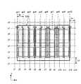
図1において、x1〜x13は自動配置配線で用いられるX方向に並ぶ配線グリッド、y1〜y8はY方向に並ぶ配線グリッド、C1,C2,C3はスタンダードセル、O1,O2,O3はC1,C2,C3の原点、TはスタンダードセルCi(i=1,2…)の入力信号または出力信号を伝達可能な端子、Gはゲート電極である。 In FIG. 1, x1 to x13 are wiring grids arranged in the X direction used in automatic placement and routing, y1 to y8 are wiring grids arranged in the Y direction, C1, C2, and C3 are standard cells, and O1, O2, and O3 are C1, C2 , C3, T is a terminal capable of transmitting an input signal or an output signal of the standard cell Ci (i = 1, 2,...), And G is a gate electrode.
自動配置配線ツールは、セル、ブロックの配置と端子間の配線経路を決定する自動設計処理ツールである。自動設計処理ツールは、コンピュータでその演算処理が実行されるプログラムから構成されており、予めコンピュータにインストールされたうえで使用される。 The automatic placement and routing tool is an automatic design processing tool that determines the layout of cells and blocks and the wiring route between terminals. The automatic design processing tool is composed of a program for executing the arithmetic processing by a computer, and is used after being installed in the computer in advance.
このような自動配置配線ツールを用いることで、X方向、Y方向の配線グリッド上に最小配線幅で配線することが可能となる。配線される配線グリッドどうしは、X方向にLxの等間隔、Y方向にLyの等間隔に配置される。X方向での配線とY方向での配線とは、基本的に別の配線層を使用し、異なる配線層間は層間接続により接続される。 By using such an automatic placement and routing tool, it is possible to perform wiring with the minimum wiring width on the wiring grid in the X direction and the Y direction. Wiring grids to be wired are arranged at equal intervals of Lx in the X direction and at equal intervals of Ly in the Y direction. The wiring in the X direction and the wiring in the Y direction basically use different wiring layers, and different wiring layers are connected by interlayer connection.
端子Tを構成する配線は、X方向に沿って横長の矩形形状(長方形)を有する。端子Tの短辺寸法は、自動配置配線での配線幅Wとなっている。また、長辺寸法は、(X方向グリッド間隔Lx+配線幅W)以上となっている。 The wiring constituting the terminal T has a horizontally long rectangular shape (rectangle) along the X direction. The short side dimension of the terminal T is the wiring width W in automatic placement and routing. The long side dimension is equal to or greater than (X-direction grid interval Lx + wiring width W).
自動配置配線ツールを用いて端子Tに配線接続を行うためには、端子Tはグリッド交点(配線グリッドの交点)を含まなければならない(黒丸●参照)。実施の形態1では、端子Tを横長(X方向に長い)矩形状とし、Y方向に並ぶ配線グリッドyi(i=1,2…)上に配置している。 In order to perform wiring connection to the terminal T using the automatic placement and routing tool, the terminal T must include a grid intersection (intersection of the wiring grid) (see black circles ●). In the first embodiment, the terminal T has a horizontally long (long in the X direction) rectangular shape and is arranged on a wiring grid yi (i = 1, 2,...) Arranged in the Y direction.
実施の形態1とは逆に、図3に示すように、端子Tを構成する配線をY方向に縦長(Y方向に長い)矩形状にした場合、楕円で囲んだ部分のように、グリッド交点に配置されない端子Tが存在する。これは、従来技術の図17と同じ状況である。 In contrast to the first embodiment, as shown in FIG. 3, when the wiring constituting the terminal T is formed in a vertically long (long in the Y direction) rectangular shape in the Y direction, a grid intersection is formed like a portion surrounded by an ellipse. There are terminals T that are not arranged in This is the same situation as in FIG.
実施の形態1のように、端子Tの長辺寸法を(X方向グリッド間隔Lx+配線幅W)とした横長矩形状とすることで、図2の端子T11,T17に例示されるように、端子Tは、配線グリッドの交点と最大2箇所で交差する。さらには、端子T11,T17の状態からX方向にずれた場合でも、端子T12〜T16に例示されるように、少なくとも1個のグリッド交点と交差する。As illustrated in the first embodiment, the terminals T11 and T17 in FIG. 2 are exemplified by having a horizontally long rectangular shape in which the long side dimension of the terminal T is (X-direction grid interval Lx + wiring width W). The terminal T intersects with the intersection of the wiring grid at a maximum of two locations. Furthermore, even when it deviates from the state of the terminals T11 and T17 in the X direction, as illustrated in the terminals T12 to T16 , it intersects with at least one grid intersection.
実施の形態1によれば、セル配置位置をY方向では限定するものの、X方向では任意位置としても、少なくとも1箇所の配線グリッド交点に端子Tを配置することができる。したがって、全端子Tを配線グリッド上に配置するために、図17の従来技術のセルC51,C52,C53に示すように、各セル原点をX方向でのグリッド間中点に配置する必要がなくなる。つまり、全端子Tを配線グリッド上に配置するための余分な領域R1,R2,R3をセル内に設ける必要がなくなる。あるいは、セル間に無駄な領域R1,R2,R3が発生することがなくなる。以上の結果として、チップサイズを小さくすることができるようになる。 According to the first embodiment, although the cell arrangement position is limited in the Y direction, the terminal T can be arranged at at least one wiring grid intersection even if the cell arrangement position is arbitrary in the X direction. Therefore, in order to arrange all the terminals T on the wiring grid, as shown in the prior art cells C51, C52, C53 of FIG. 17, it is not necessary to arrange each cell origin at the midpoint between the grids in the X direction. . That is, it is not necessary to provide extra regions R1, R2, and R3 for arranging all the terminals T on the wiring grid in the cell. Alternatively, useless regions R1, R2, and R3 are not generated between cells. As a result, the chip size can be reduced.
なお、端子Tを構成する配線の長辺寸法の上限値は、実質上、X方向に沿うセルCのセル幅から配線の最小間隔を差し引いた長さ以下となる。また、上述したように、面積効率からみて、端子Tを構成する配線の長辺寸法は、(X方向グリッド間隔Lx+配線幅W)とするのが好ましい。しかしながら、(X方向グリッド間隔Lx+配線幅W)の値は、端子Tを構成する配線の長辺寸法の下限値として見なしてもよい。 Note that the upper limit value of the long side dimension of the wiring configuring the terminal T is substantially equal to or smaller than the length obtained by subtracting the minimum wiring interval from the cell width of the cell C along the X direction. Further, as described above, in view of area efficiency, it is preferable that the long side dimension of the wiring configuring the terminal T is (X-direction grid interval Lx + wiring width W). However, the value of (X-direction grid interval Lx + wiring width W) may be regarded as the lower limit value of the long side dimension of the wiring constituting the terminal T.
以上説明した実施の形態1では、ロジックブロックを合成して設計する際のスタンダードセルにおいて本発明を実施した。しかしながら、実施の形態1では、ゲートピッチが予め設定されているゲートアレイセルにおいても同様に実施することができる。この場合、ゲートアレイセルの端子形状を上述したスタンダードセルの端子形状と同様にすればよく、図面上の構成は全く変わらない。そうすれば、スタンダードセルの場合と同様のセル面積縮小効果が得られる。あるいは、ゲートアレイセルのゲートピッチまで配線グリットを拡大することによるブロック面積の増大を抑えることができる。 In the first embodiment described above, the present invention is implemented in a standard cell when a logic block is synthesized and designed. However, in the first embodiment, the same can be applied to the gate array cell in which the gate pitch is set in advance. In this case, the terminal shape of the gate array cell may be the same as that of the standard cell described above, and the configuration on the drawing is not changed at all. Then, the same cell area reduction effect as in the standard cell can be obtained. Alternatively, it is possible to suppress an increase in the block area caused by expanding the wiring grid to the gate pitch of the gate array cell.
ここで、図1は、実施の形態1で説明したセルを用いて設計された半導体集積回路の一部でもある。上述のセルを使用することで、集積回路の小面積化が実現できることはいうまでもない。 Here, FIG. 1 is also a part of a semiconductor integrated circuit designed using the cell described in the first embodiment. It goes without saying that the area of the integrated circuit can be reduced by using the above-described cells.
なお、図4に示すように、実施の形態1では、必ずしもセル幅がLxの整数倍でないセルの原点を隣接するX方向配線グリッド間の中点に配置する必要性は必ずしもない。図4に示す構成としても上述した実施の形態1と同様の効果を得ることができる。 As shown in FIG. 4, in the first embodiment, it is not always necessary to place the origin of a cell whose cell width is not an integral multiple of Lx at the midpoint between adjacent X-direction wiring grids. Also with the configuration shown in FIG. 4, the same effects as those of the first embodiment described above can be obtained.
(実施の形態2)
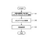
図5は、本発明の実施の形態2におけるスタンダードセルの自動配置配線方法の処理フローを表わす。(Embodiment 2)
FIG. 5 shows a processing flow of the standard cell automatic placement and routing method according to the second embodiment of the present invention.
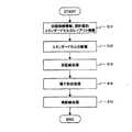
この自動配置配線方法を実行する自動配置配線装置は、論理回路の接続情報を外部から獲得する接続情報入力手段と、論理回路の設計規約を外部から獲得する設計規約入力手段と、スタンダードセルのレイアウト情報を外部から獲得するレイアウト情報入力手段と、獲得した接続情報に基づいて各セル群を仮配置する仮配置手段と、仮配置した各セル群を面積小になるように再配置する再配置手段とを備える。このような構成を有する自動配置配線装置は複数のスタンダードセルを含む状態で論理回路を配置配線する。 An automatic placement and routing apparatus for executing this automatic placement and routing method includes a connection information input means for acquiring logic circuit connection information from the outside, a design rule input means for acquiring logic circuit design rules from the outside, and a standard cell layout. Layout information input means for acquiring information from outside, temporary placement means for temporarily placing each cell group based on the acquired connection information, and rearrangement means for rearranging each temporarily placed cell group so as to reduce the area With. The automatic placement and routing apparatus having such a configuration places and routes a logic circuit in a state including a plurality of standard cells.
まず、予め、複数のスタンダードセルどうしを互いに接続するための論理回路の回路接続情報、自動配置配線を行う際に必要となる設計規約、および各スタンダードセルのレイアウトデータを図示しない記憶装置に格納しておく。ここで記憶装置に格納されるレイアウト情報は、セルC21,C22,C23として、実施の形態1で説明した構造を有するセルのレイアウト情報である。 First, the circuit connection information of logic circuits for connecting a plurality of standard cells to each other, the design rules necessary for automatic placement and routing, and the layout data of each standard cell are stored in a storage device (not shown). Keep it. Here, the layout information stored in the storage device is the layout information of the cells having the structure described in the first embodiment as the cells C21, C22, and C23.
そのうえで、自動配置配線装置は、データ読み込み工程S1において、上述した回路接続情報、設計規約、および各スタンダードセルのレイアウトデータを記憶装置から読み出す。 In addition, the automatic placement and routing apparatus reads the above-described circuit connection information, design rules, and layout data of each standard cell from the storage device in the data reading step S1.
次に、自動配置配線装置は、仮配置工程S2において、図6に示すように、第1のスタンダードセルC21,C22,C23の原点O21,O22,O23がX方向の隣接配線グリッド間の中点およびY方向の隣接配線グリッド間の中点に位置するように、回路接続情報に基づいてセルC21,C22,C23を仮配置する。ここで第1のスタンダードセルC21,C22,C23とは、実施の形態1で説明した構造を有するセルであって、各セル幅が必ずしも自動配置配線での配線グリッド間隔の整数倍ではないセルのことである。 Next, in the temporary placement and routing apparatus, in the temporary placement step S2, as shown in FIG. 6, the origins O21, O22, and O23 of the first standard cells C21, C22, and C23 are midpoints between adjacent wiring grids in the X direction. The cells C21, C22, and C23 are temporarily arranged based on the circuit connection information so as to be positioned at the midpoint between adjacent wiring grids in the Y direction. Here, the first standard cells C21, C22, and C23 are cells having the structure described in the first embodiment, and each cell width is not necessarily an integral multiple of the wiring grid interval in automatic placement and routing. That is.
次いで、自動配置配線装置は、再配置工程S3において、まず、仮配置したスタンダードセルのセル原点のY座標が、自動配置配線での隣接配線グリッド間の中点または配線グリッド上に位置するとともに、セル原点のX座標が、隣接配線グリッド間の中点または前記配線グリッド上に位置するセルを抽出する。図6の例では、セルC21,C22,C23が抽出される。 Next, the automatic placement and routing apparatus, in the rearrangement step S3, first, the Y coordinate of the cell origin of the temporarily placed standard cell is located on the midpoint between adjacent wiring grids in the automatic placement and routing or on the wiring grid, A cell in which the X coordinate of the cell origin is located at the midpoint between adjacent wiring grids or on the wiring grid is extracted. In the example of FIG. 6, cells C21, C22, and C23 are extracted.
次いで、自動配置配線装置は、再配置工程S3において、抽出したセルC21,C22,C23を、隣接する余分な領域R21,R22,R23をなくすようにX方向に移動して互いのセル枠が当接してロジック部の面積が小さくなるように、セルC21,C22,C23を再配置する。 Next, in the rearrangement step S3, the automatic placement and routing apparatus moves the extracted cells C21, C22, and C23 in the X direction so as to eliminate the adjacent extra regions R21, R22, and R23, and the mutual cell frames are matched. The cells C21, C22, and C23 are rearranged so that the area of the logic portion is reduced in contact.
その後、自動置配線装置は、実配線処理工程S4において、それぞれ配置されたセルC21,C22,C23どうしの配線処理を行う。 Thereafter, the automatic placement and routing apparatus performs wiring processing between the cells C21, C22, and C23 arranged in the actual wiring processing step S4.
再配置工程S3を実行することで、仮配置工程S2での領域R21,R22(斜線部)を省略することができ、ロジック面積を小さくし、ひいては、チップサイズを小さくすることができるようになる。 By executing the rearrangement step S3, the regions R21 and R22 (shaded portions) in the temporary arrangement step S2 can be omitted, the logic area can be reduced, and consequently the chip size can be reduced. .
(実施の形態3)
図7は、本発明の実施の形態3におけるスタンダードセルの自動配置配線方法の処理フローを表わす。(Embodiment 3)
FIG. 7 shows a processing flow of the standard cell automatic placement and routing method according to the third embodiment of the present invention.
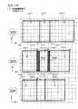
この自動配置配線方法を実行する自動配置配線装置は、論理回路の接続情報を外部から獲得する接続情報入力手段と、論理回路の設計規約を外部から獲得する設計規約入力手段と、スタンダードセルのレイアウト情報を外部から獲得するレイアウト情報入力手段と、獲得した接続情報に基づいて各セル群を配置する配置手段と、各セルの端子を接続する配線の仮配線を行う仮配線処理手段と、端子を形成する端子形状処理手段と、実配線処理手段とを備える。 An automatic placement and routing apparatus for executing this automatic placement and routing method includes a connection information input means for acquiring logic circuit connection information from the outside, a design rule input means for acquiring logic circuit design rules from the outside, and a standard cell layout. Layout information input means for acquiring information from the outside, placement means for arranging each cell group based on the acquired connection information, temporary wiring processing means for performing temporary wiring of wiring for connecting terminals of each cell, and terminals Terminal shape processing means to be formed and actual wiring processing means are provided.
まず、予め、複数のスタンダードセルどうしを互いに接続するための論理回路の回路接続情報、自動配置配線を行う際に必要となる設計規約、および各スタンダードセルのレイアウトデータを図示しない記憶装置に格納しておく。ここで記憶装置に格納されるレイアウト情報は、セルC11,C12,C13として、実施の形態1で説明した構造を有するセルのレイアウト情報に基本的に類似した構造を有するレイアウト情報であるが、その詳細については次に説明する。 First, the circuit connection information of logic circuits for connecting a plurality of standard cells to each other, the design rules necessary for automatic placement and routing, and the layout data of each standard cell are stored in a storage device (not shown). Keep it. Here, the layout information stored in the storage device is layout information having a structure basically similar to the layout information of the cells having the structure described in the first embodiment as the cells C11, C12, and C13. Details will be described next.
そのうえで、自動配置配線装置は、データ読み込み工程S11において、複数のセルどうしを互いに接続するための論理回路の回路接続情報、自動配置配線を行う際に必要な設計規約、および各セルのレイアウトデータを記憶装置から読み出す。このとき読み出されるレイアウトデータは、上述したように基本的には、実施の形態1で説明した構造を有するものの、図8に示すように、端子Tの長辺寸法はX方向に沿ったセル幅から配線の最小間隔を差し引いた長さに設定されている。なお、端子Tの長辺寸法は後の工程で短縮される。また、セル幅は、必ずしも自動配置配線での配線グリッド間隔の整数倍ではない。 In addition, in the data reading step S11, the automatic placement and routing apparatus obtains circuit connection information of logic circuits for connecting a plurality of cells to each other, design rules necessary for automatic placement and routing, and layout data of each cell. Read from storage device. The layout data read at this time basically has the structure described in the first embodiment as described above. However, as shown in FIG. 8, the long side dimension of the terminal T is the cell width along the X direction. It is set to the length obtained by subtracting the minimum wiring interval from. The long side dimension of the terminal T is shortened in a later process. The cell width is not necessarily an integer multiple of the wiring grid interval in automatic placement and routing.
次に、自動配置配線装置は、スタンダードセルの配置工程S12において、セル原点O31,O32,O33がY方向の隣接配線グリッド間の中点に位置するように、回路接続情報に基づいてセルC31,C32,C33を配置する。 Next, in the standard cell placement step S12, the automatic placement and routing apparatus performs cell C31, cell C31, based on the circuit connection information so that the cell origins O31, O32, and O33 are positioned at the midpoint between adjacent wiring grids in the Y direction. C32 and C33 are arranged.
次いで、自動配置配線装置は、仮配線処理工程S13において、回路接続情報に基づいて複数の端子Tを配線で接続する。このとき、端子Tの形状がX方向に長細いので、仮配線する際に自由度が上がり、全配線長を短くすることができる。 Next, the automatic placement and routing apparatus connects the plurality of terminals T by wiring based on the circuit connection information in the temporary wiring processing step S13. At this time, since the shape of the terminal T is long and thin in the X direction, the degree of freedom is increased when provisional wiring is performed, and the total wiring length can be shortened.
その後、自動配置配線装置は、端子形状処理工程S14において、有効な接続にとって必要な端子形状寸法を自動で認識し、端子Tにおいて不要な部分を削除し、端子形状の縮小を行う。 Thereafter, in the terminal shape processing step S14, the automatic placement and routing apparatus automatically recognizes the terminal shape dimensions necessary for effective connection, deletes unnecessary portions from the terminal T, and reduces the terminal shape.
最後に、自動配置配線装置は、実配線処理工程S15において、スタンダードセルどうしの配線処理を行う。端子形状処理工程S14での端子縮小により配線リソースが増加しているので、その配線リソースを最大限に活かす状態でスタンダードセルどうしの配線処理を行う。 Finally, the automatic placement and routing apparatus performs wiring processing between standard cells in the actual wiring processing step S15. Since the wiring resources have increased due to the terminal reduction in the terminal shape processing step S14, the wiring processing between the standard cells is performed in a state where the wiring resources are utilized to the maximum.
上記の工程S11〜S15を実行することで、結果として全配線長を短くすることができ、配線容量削減、遅延時間削減、配線リソース増による設計TATの短縮を実現できる。 By executing the above steps S11 to S15, the total wiring length can be shortened as a result, and it is possible to reduce the wiring capacity, the delay time, and the design TAT by increasing the wiring resources.
また、全端子Tを配線グリッド上に配置するために、図17の従来技術のセルC51,C52,C53のように各セル原点をX方向でのグリッド間中点に配置する必要がなくなる。つまり、全端子Tを配線グリッド上に配置するための領域R1,R2,R3をセル内に設ける必要がなくなる。あるいは、セル間に領域R1,R2,R3が発生しなくなる。以上の結果として、チップサイズを小さくすることができる。 Further, since all the terminals T are arranged on the wiring grid, it is not necessary to arrange each cell origin at the midpoint between the grids in the X direction as in the conventional cells C51, C52, C53 of FIG. That is, it is not necessary to provide the regions R1, R2, and R3 for arranging all the terminals T on the wiring grid in the cell. Alternatively, the regions R1, R2, and R3 are not generated between cells. As a result, the chip size can be reduced.
(実施の形態4)
図9は、本発明の実施の形態4におけるスタンダードセルの自動配置配線方法の処理フローを表わす。(Embodiment 4)
FIG. 9 shows the processing flow of the standard cell automatic placement and routing method according to the fourth embodiment of the present invention.
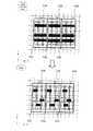
この自動配置配線方法を実行する自動配置配線装置は、論理回路の接続情報を外部から獲得する接続情報入力手段と、論理回路の設計規約を外部から獲得する設計規約入力手段と、セル幅が配線グリッド間隔の整数倍であるスタンダードセルライブラリのレイアウト情報およびセル幅が必ずしも配線グリッド間隔の整数倍でないスタンダードセルライブラリのレイアウト情報を外部から獲得するレイアウト情報入力手段と、セル幅が配線グリッド間隔の整数倍であるスタンダードセルライブラリのセルを上記接続情報に基づいて配置する配置手段と、配置された各セルをセル幅が必ずしも配線グリッド間隔の整数倍ではないスタンダードセルライブラリの同じ論理のセルに置換するセル置換手段と、セル配置面積を圧縮するために各セルを再配置する再配置手段と、再配置されたセル同士を上記接続情報に基づいて配線により接続する実配線処理手段とを備える。 An automatic placement and routing apparatus that executes this automatic placement and routing method includes connection information input means for acquiring logic circuit connection information from the outside, design rule input means for acquiring logic circuit design rules from the outside, and cell width wiring Layout information input means for obtaining externally the layout information of the standard cell library that is an integer multiple of the grid interval and the standard cell library layout information and the cell width is not necessarily an integer multiple of the wiring grid interval, and the cell width is an integer of the wiring grid interval The placement means for placing the cells of the standard cell library which is twice based on the above connection information, and the placed cells are replaced with cells of the same logic in the standard cell library whose cell width is not necessarily an integral multiple of the wiring grid interval. Cell replacement means and re-reach each cell to reduce cell placement Comprising a rearrangement unit that location, the cell together rearranged the actual routing processing means for connecting the wiring based on the connection information.
なお、セル幅が配線グリッド間隔の整数倍であるスタンダードセルのグループを、以下第1のセル群といい、セル幅が必ずしも配線グリッド間隔の整数倍でないスタンダードセルのグループを第2のセル群という。 A group of standard cells whose cell width is an integral multiple of the wiring grid interval is hereinafter referred to as a first cell group, and a group of standard cells whose cell width is not necessarily an integer multiple of the wiring grid interval is referred to as a second cell group. .
まず、予め、複数のスタンダードセルどうしを互いに接続するための論理回路の回路接続情報、自動配置配線を行う際に必要となる設計規約、および各スタンダードセルのレイアウトデータを図示しない記憶装置に格納しておく。ここで記憶装置に格納されるレイアウト情報は、セルC11,C12,C13として、実施の形態1で説明した構造を有するセルのレイアウト情報に基本的に類似した構造を有するレイアウト情報である。ただし、このレイアウト情報は、第1のセル群のレイアウト情報と、第2のセル群のレイアウト情報とを含む。 First, the circuit connection information of logic circuits for connecting a plurality of standard cells to each other, the design rules necessary for automatic placement and routing, and the layout data of each standard cell are stored in a storage device (not shown). Keep it. Here, the layout information stored in the storage device is layout information having a structure basically similar to the layout information of the cells having the structure described in the first embodiment as the cells C11, C12, and C13. However, this layout information includes the layout information of the first cell group and the layout information of the second cell group.
そのうえで、自動配置配線装置は、データ読み込み工程S21において、複数のスタンダードセルどうしを互いに接続するための論理回路の回路接続情報、自動配置配線を行う際に必要な設計規約、第1のセル群のレイアウトデータ、および第2のセル群のレイアウトデータを記憶装置から読み出す。 In addition, in the data reading step S21, the automatic placement and routing apparatus includes circuit connection information of logic circuits for connecting a plurality of standard cells to each other, design rules necessary for automatic placement and routing, and the first cell group. The layout data and the layout data of the second cell group are read from the storage device.
次に、自動配置配線装置は、仮配置工程S22においては、図10に示すように、レイアウト情報を読み出した第1のセルCb11,Cb12,Cb13を、その原点Ob11,Ob12,Ob13がX方向の隣接配線グリッド間の中点およびY方向の隣接配線グリッド間の中点に位置するように、回路接続情報に基づいて仮配置する。 Next, in the temporary placement and routing apparatus, in the temporary placement step S22, as shown in FIG. 10, the first cells Cb11, Cb12, and Cb13 from which the layout information has been read are set to the origins Ob11, Ob12, and Ob13 in the X direction. Temporary placement is performed based on the circuit connection information so as to be positioned at a midpoint between adjacent wiring grids and a midpoint between adjacent wiring grids in the Y direction.
次に、セル置換工程S23においては、第1のセルCb11,Cb12,Cb13を、それぞれ同じ論理で、第2のセルCb21,Cb22,Cb23に置換する。このとき、第2のセルCb21,Cb22,Cb23の原点Ob21,Ob22,Ob23を、セルCb11,Cb12,Cb13の原点Ob11,Ob12,Ob13と同一の座標にする。 Next, in the cell replacement step S23, the first cells Cb11, Cb12, Cb13 are replaced with the second cells Cb21, Cb22, Cb23, respectively, with the same logic. At this time, the origins Ob21, Ob22, Ob23 of the second cells Cb21, Cb22, Cb23 are set to the same coordinates as the origins Ob11, Ob12, Ob13 of the cells Cb11, Cb12, Cb13.
次いで、再配置工程S24においては、トータルのセル配置面積が小さくなるように、第2のセルCb21,Cb22,Cb23をX方向に移動させる再配置を行なう。その移動量は、隣接するセル同士のセル枠が接するところを最大とする。 Next, in the rearrangement step S24, rearrangement is performed by moving the second cells Cb21, Cb22, and Cb23 in the X direction so that the total cell arrangement area is reduced. The amount of movement is maximized when the cell frames of adjacent cells touch each other.
その後、実配線処理工程S25においては、回路接続情報に基づき、再配置された第2のセルCb21,Cb22,Cb23同士の配線処理を行う。 Thereafter, in the actual wiring processing step S25, wiring processing between the rearranged second cells Cb21, Cb22, and Cb23 is performed based on the circuit connection information.
以上のようなフローにより、セル幅が必ずしも配線グリッド間隔の整数倍でない第2のセルを直接扱えない自動配置配線ツールにおいても、図10に示される領域Rb21,Rb22(斜線部)を省略することができる。そのため、スタンダードセルで構成されるロジック面積を小さくし、ひいては、チップサイズを小さくすることができる。 With the above flow, even in the automatic placement and routing tool that cannot directly handle the second cell whose cell width is not necessarily an integer multiple of the wiring grid interval, the regions Rb21 and Rb22 (shaded portions) shown in FIG. 10 are omitted. Can do. Therefore, it is possible to reduce the logic area composed of standard cells, and thus the chip size.
(実施の形態5)
図11は、本発明の実施の形態5におけるスタンダードセルのレイアウト図である。ここで、スタンダードセルの電源配線に沿った方向をX方向、電源配線Sに対して垂直な方向をY方向とする。なお、図例の電源配線Sはその一例であって電源配線Sはこのような位置に限定されない。(Embodiment 5)
FIG. 11 is a layout diagram of a standard cell according to the fifth embodiment of the present invention. Here, a direction along the power supply wiring of the standard cell is defined as an X direction, and a direction perpendicular to the power supply wiring S is defined as a Y direction. In addition, the power supply wiring S of the example is an example, and the power supply wiring S is not limited to such a position.
図11において、x1〜x13は自動配置配線で用いられる、Y方向に平行に配置されて互いにX方向に並ぶ配線グリッド、y1〜y8はX方向に平行に配置されて互いにY方向に並ぶ配線グリッド、gx1〜gx10は自動配置配線に用いられるY方向に平行に配置されて互いにX方向に並ぶゲートピッチのグリッド、C61,C62,C63はスタンダードセル、O61,O62,O63はスタンダードセルC61,C62,C63の原点、TはスタンダードセルCi(i=1,2…)における入力信号または出力信号を伝達可能な端子、Gはゲート電極、DGはダミーゲート電極である。 In FIG. 11, x1 to x13 are wiring grids used in automatic placement and routing, wiring grids arranged parallel to the Y direction and arranged in the X direction, and y1 to y8 are wiring grids arranged parallel to the X direction and arranged in the Y direction. , Gx1 to gx10 are gate pitch grids arranged in parallel to the Y direction used for automatic placement and routing, and arranged in the X direction, C61, C62, C63 are standard cells, O61, O62, O63 are standard cells C61, C62, The origin of C63, T is a terminal capable of transmitting an input signal or an output signal in the standard cell Ci (i = 1, 2,...), G is a gate electrode, and DG is a dummy gate electrode.
さらにスタンダードセルC61,C62,C63においては、ゲート電極G,ダミーゲート電極DGのゲート長、ゲート間隔は互いに一定となっており、かつ各スタンダードセルC61,C62,C63のX方向のセル幅はゲートピッチGx(ゲートピッチはゲート長にゲート間隔を足した値)の最小値の整数倍となっている(図11においては、スタンダードセルC61,C62,C63のセル幅はGxの3倍となっている)。 Further, in the standard cells C61, C62, and C63, the gate length and the gate interval of the gate electrode G and the dummy gate electrode DG are constant, and the cell width in the X direction of each standard cell C61, C62, and C63 is the gate. It is an integral multiple of the minimum value of the pitch Gx (the gate pitch is a value obtained by adding the gate interval to the gate length) (in FIG. 11, the cell widths of the standard cells C61, C62, C63 are three times the Gx). )
自動配置配線ツールは、セル、ブロックの配置と端子間の配線経路を決定する自動設計処理ツールである。自動配置配線ツールは、上述した各実施の形態とその構成は同一である。 The automatic placement and routing tool is an automatic design processing tool that determines the layout of cells and blocks and the wiring route between terminals. The automatic placement and routing tool has the same configuration as each embodiment described above.
自動配置配線ツールの配置の際においては、各セルのX方向のセル幅がゲートピッチGxの整数倍となっているため、各セルのX方向の配置をゲートピッチのグリッドの位置に配置することができる。 When the automatic placement and routing tool is placed, the cell width in the X direction of each cell is an integral multiple of the gate pitch Gx, so the placement of each cell in the X direction should be placed at the gate pitch grid position. Can do.
自動配置配線ツールを用いることで、X方向、Y方向の配線グリッド上に最小配線幅で配線を配置することができる。配線グリッドは、X方向にゲートピッチGxとは異なるLxの等間隔、Y方向にLyの等間隔となっている。X方向での配線とY方向での配線とは、基本的に別の配線層を使用し、異なる配線層間は層間接続により接続される。 By using the automatic placement and routing tool, it is possible to arrange the wiring with the minimum wiring width on the wiring grid in the X direction and the Y direction. The wiring grid has an equal interval of Lx different from the gate pitch Gx in the X direction and an equal interval of Ly in the Y direction. The wiring in the X direction and the wiring in the Y direction basically use different wiring layers, and different wiring layers are connected by interlayer connection.
端子Tを構成する配線は、X方向に沿って横長の矩形形状(長方形)を有する。端子Tの短辺寸法は、自動配置配線での配線幅Wとなっている。また、長辺寸法は、(X方向グリッド間隔Lx+配線幅W)以上となっている。 The wiring constituting the terminal T has a horizontally long rectangular shape (rectangle) along the X direction. The short side dimension of the terminal T is the wiring width W in automatic placement and routing. The long side dimension is equal to or greater than (X-direction grid interval Lx + wiring width W).
自動配置配線ツールを用いて端子Tに配線接続を行うためには、端子Tはグリッド交点(配線グリッドの交点)を含まなければならない(黒丸●参照)。実施の形態6では、端子Tを横長(X方向に長い)矩形状とし、Y方向に並ぶ配線グリッドyi(i=1,2…)に配置している。 In order to perform wiring connection to the terminal T using the automatic placement and routing tool, the terminal T must include a grid intersection (intersection of the wiring grid) (see black circles ●). In the sixth embodiment, the terminals T have a horizontally long (long in the X direction) rectangular shape and are arranged on the wiring grid yi (i = 1, 2,...) Arranged in the Y direction.
実施の形態6とは逆に、図13に示すように、端子Tを構成する配線をY方向に縦長(Y方向に長い)矩形状にした場合、楕円で囲んだ部分のように、グリッド交点に配置されない端子Tが存在する。これは、従来技術の図17と同じ状況である。 In contrast to the sixth embodiment, as shown in FIG. 13, when the wiring constituting the terminal T is formed in a rectangular shape that is vertically long in the Y direction (long in the Y direction), the grid intersection point is as in the part surrounded by an ellipse. There are terminals T that are not arranged in This is the same situation as in FIG.
実施の形態6のように、端子Tの長辺寸法を(X方向グリッド間隔Lx+配線幅W)とした横長矩形状とすることで、図12の端子T11,T17に例示されるように、端子Tは、配線グリッド交点と最大2箇所で交差する。さらには、端子T11,T17の状態からX方向にずれた場合でも、端子T12〜T16に例示されるように、少なくとも1個のグリッド交点と交差する。As illustrated in the sixth embodiment, the terminals T11 and T17 in FIG. 12 are exemplified by forming a horizontally long rectangular shape with the long side dimension of the terminal T being (X-direction grid interval Lx + wiring width W). The terminal T intersects the wiring grid intersection at a maximum of two places. Furthermore, even if the deviation from the state of the terminalT11, T 17 in the X direction, as illustrated in the terminalT 12through T 16, intersects the at least one grid intersection.
実施の形態6によれば、セル配置位置をY方向では限定するものの、X方向では配線グリッドLxと異なるゲートピッチGxの整数倍の位置としても、少なくとも1箇所の配線グリッド交点に端子Tを配置することができる。したがって、全端子Tを配線グリッド上に配置するために、図19の従来技術のセルC51,C52,C53に示すように、各セル原点をX方向でのグリッド間中点に配置する必要がなくなる。つまり、全端子Tを配線グリッド上に配置するための余分な領域R1,R2,R3をセル内に設ける必要がなくなる。あるいは、セル間に無駄な領域R1,R2,R3が発生することがなくなる。以上の結果として、チップサイズを小さくすることができるようになる。 According to the sixth embodiment, although the cell arrangement position is limited in the Y direction, the terminal T is arranged at at least one wiring grid intersection even in the X direction even if the position is an integer multiple of the gate pitch Gx different from the wiring grid Lx. can do. Therefore, in order to arrange all the terminals T on the wiring grid, as shown in the prior art cells C51, C52, C53 of FIG. 19, it is not necessary to arrange each cell origin at the midpoint between the grids in the X direction. . That is, it is not necessary to provide extra regions R1, R2, and R3 for arranging all the terminals T on the wiring grid in the cell. Alternatively, useless regions R1, R2, and R3 are not generated between cells. As a result, the chip size can be reduced.
さらには、スタンダードセルC61,C62,C63の内部だけでなく、これらスタンダードセルC61,C62,C63どうしを比較しても、そのゲート電極、ダミーゲート電極のパターンはゲート長、ゲート間隔ともに同一となっている。これにより、ゲート電極の仕上がり寸法の精度を高くすることができる。さらに各スタンダードセル単体で見た場合と、それを隣接して配置した状態とではゲート電極、ダミーゲート電極のゲート長、ゲート間隔のパターンが同一となっており、OPCを各スタンダードセル単体で行うことができる。 Further, not only the inside of the standard cells C61, C62, C63 but also the standard cells C61, C62, C63 are compared with each other, the patterns of the gate electrodes and the dummy gate electrodes are the same in both gate length and gate interval. ing. Thereby, the precision of the finish dimension of a gate electrode can be made high. Furthermore, the gate electrode and the dummy gate electrode have the same gate length and gate interval pattern when viewed as a single standard cell and when adjacent to each other, and OPC is performed for each standard cell alone. be able to.
なお、端子Tを構成する配線の長辺寸法の上限値は、実質上、X方向に沿うセルCのセル幅から配線の最小間隔を差し引いた長さ以下となる。また、上述したように、面積効率からみて、端子Tを構成する配線の長辺寸法は、(X方向グリッド間隔Lx+配線幅W)とするのが好ましい。しかしながら、(X方向グリッド間隔Lx+配線幅W)の値は、端子Tを構成する配線の長辺寸法の下限値として見なしてもよい。 Note that the upper limit value of the long side dimension of the wiring configuring the terminal T is substantially equal to or smaller than the length obtained by subtracting the minimum wiring interval from the cell width of the cell C along the X direction. Further, as described above, in view of area efficiency, it is preferable that the long side dimension of the wiring configuring the terminal T is (X-direction grid interval Lx + wiring width W). However, the value of (X-direction grid interval Lx + wiring width W) may be regarded as the lower limit value of the long side dimension of the wiring constituting the terminal T.
以上説明した実施の形態5では、ロジックブロックを合成して設計する際のスタンダードセルにおいて本発明を実施した。しかしながら、実施の形態6では、ゲートピッチが予め設定されているゲートアレイセルにおいても同様に実施することができる。この場合、ゲートアレイセルの端子形状を上述したスタンダードセルの端子形状と同様にすればよい。そうすれば、スタンダードセルの場合と同様のセル面積縮小効果が得られる。あるいは、ゲートアレイセルのゲートピッチまで配線グリットを拡大することに起因して生じるブロック面積の増大を抑えることができる。 In the fifth embodiment described above, the present invention is implemented in the standard cell when the logic block is synthesized and designed. However, the sixth embodiment can be similarly implemented in a gate array cell in which the gate pitch is set in advance. In this case, the terminal shape of the gate array cell may be the same as the terminal shape of the standard cell described above. Then, the same cell area reduction effect as in the standard cell can be obtained. Alternatively, it is possible to suppress an increase in block area caused by expanding the wiring grid to the gate pitch of the gate array cell.
なお、実施の形態5においては、ゲート電極、ダミーゲート電極は全て同一のゲート長であるとしたが、同一である必要はない。図14にゲート電極、ダミーゲート電極の一部のゲート長が同一でないスタンダードセルの例を示す。 In the fifth embodiment, the gate electrodes and the dummy gate electrodes all have the same gate length, but need not be the same. FIG. 14 shows an example of a standard cell in which the gate length of part of the gate electrode and the dummy gate electrode is not the same.
図14において、C81はスタンダードセルである。スタンダードセルC81内にはゲート電極Gと、ダミーゲート電極DGと、さらにはゲート長がゲート電極G、ダミーゲート電極DGとは異なるゲート電極G2が二つ設けられており、スタンダードセルC81のX方向のセル幅はゲートピッチGxの整数倍となるように、ゲート電極G2の幅が設定されている。なお、図14においては、スタンダードセルC81のセル幅はゲートピッチGxの9倍となっている。ここで、G2の幅をこのように設定するのは、一般的に用いられる自動配置配線ツールで配置を行う際において、各セルのX方向のセル幅がゲートピッチGxの整数倍となっている方が各セルのセル幅が任意の値を取る場合に比べて処理速度が速いと予想されるためであり、必ずしもこのようにゲート電極G2の幅を設定する必要はない。なお、説明を簡単にするため、図14では端子を記載していない。 In FIG. 14, C81 is a standard cell. In the standard cell C81, a gate electrode G, a dummy gate electrode DG, two gate electrodes G2 having a gate length different from the gate electrode G and the dummy gate electrode DG are provided. The width of the gate electrode G2 is set so that the cell width becomes an integer multiple of the gate pitch Gx. In FIG. 14, the cell width of the standard cell C81 is nine times the gate pitch Gx. Here, the width of G2 is set in this way because the cell width in the X direction of each cell is an integral multiple of the gate pitch Gx when performing placement with a generally used automatic placement and routing tool. This is because the processing speed is expected to be faster than when the cell width of each cell takes an arbitrary value, and it is not always necessary to set the width of the gate electrode G2. For simplicity of explanation, terminals are not shown in FIG.
このようにゲート長の異なるゲート電極を有するスタンダードセルを含む場合でも、前述したように端子の長辺寸法を(X方向グリット間隔Lx+配線幅W)とする横長矩形状とすることで、端子が少なくとも1個の配線グリット交点と交差するようにしておけば、X方向のセル配置を自由に設定することができ、セル間に余分な領域が発生することはない。 Even in the case of including standard cells having gate electrodes with different gate lengths as described above, the terminals can be formed into a horizontally long rectangular shape having the long side dimension of the terminal (X-direction grid interval Lx + wiring width W) as described above. If it intersects with at least one wiring grid intersection, the cell arrangement in the X direction can be freely set, and no extra area is generated between the cells.
また、自動配置配線ツールの処理速度を考慮して、各セルのX方向のセル幅がゲートピッチGxの整数倍となるように設定した場合でも同様にセル間に余分な領域が発生することはない。また、ゲート電極、ダミーゲート電極のパターンはゲート長、ゲート間隔において、不均一な部分をスタンダードセル内に持つことができるため、スタンダードセルの設計の自由度が向上する。また、OPCを各スタンダードセル単体で行うことができる効果については他の実施の形態と同様、実施の形態6でも得られる。 In addition, in consideration of the processing speed of the automatic placement and routing tool, even when the cell width in the X direction of each cell is set to be an integral multiple of the gate pitch Gx, an extra area is similarly generated between the cells. Absent. Further, the pattern of the gate electrode and the dummy gate electrode can have a non-uniform portion in the standard cell with respect to the gate length and the gate interval, so that the degree of freedom in designing the standard cell is improved. Further, the effect that OPC can be performed for each standard cell alone is also obtained in the sixth embodiment, as in the other embodiments.
以上の説明では、ゲート長が同一ではなく互いに異なるゲート電極を設ける場合について説明したが、ゲート長が異なるダミーゲート電極を設ける場合や、ゲート間隔が異なるゲート電極やダミーゲート電極を設けるセル構成においても同様に実施の形態5を実施することができる。 In the above description, the case where the gate lengths are not the same but different gate electrodes are provided has been described. However, in the case of providing dummy gate electrodes having different gate lengths, or in the cell configuration in which gate electrodes or dummy gate electrodes having different gate intervals are provided. Similarly, the fifth embodiment can be implemented.
なお、実施の形態5においては、ダミーゲート電極DGを設けることを前提して説明したが、次の構成において実施の形態5を実施してもその効果を同様に得ることができる。その構成とは、ダミーゲート電極DGを設けない構成において、さらに各スタンダードセルのセル枠からの最近傍のゲート電極までの距離を一定にする構成である。この構成においても、各スタンダードセルのセル枠から最近傍のゲート電極までの距離と、そのスタンダードセルに隣接する他のスタンダードセルのセル枠から最近傍のゲート電極までの距離とは一定になる。そのため、このような構成においても、OPCを各スタンダードセル単体で行うことができるという実施の形態5の効果を同様に得ることができる。 Although the fifth embodiment has been described on the assumption that the dummy gate electrode DG is provided, the effect can be obtained similarly even when the fifth embodiment is implemented in the following configuration. The configuration is a configuration in which the dummy gate electrode DG is not provided and the distance from the cell frame of each standard cell to the nearest gate electrode is made constant. Also in this configuration, the distance from the cell frame of each standard cell to the nearest gate electrode and the distance from the cell frame of another standard cell adjacent to the standard cell to the nearest gate electrode are constant. Therefore, even in such a configuration, the effect of the fifth embodiment that OPC can be performed by each standard cell alone can be similarly obtained.
例えば、前述した図11の構成においてダミーゲート電極DGを設けない構成であっても、各スタンダードセルC61,C62,C63のセル枠から、各スタンダードセルの端部に位置するゲート電極GまでのX方向の距離は(Gx−ゲート長/2)であって一定であり、また、各スタンダードセルの端部に位置するゲート電極Gから、隣接するスタンダードセルの端部に位置するゲート電極GまでのX方向の距離は(2Gx−ゲート長)であって一定である。 For example, even if the dummy gate electrode DG is not provided in the configuration of FIG. 11 described above, the X from the cell frame of each standard cell C61, C62, C63 to the gate electrode G located at the end of each standard cell The distance in the direction is (Gx−gate length / 2) and is constant, and from the gate electrode G located at the end of each standard cell to the gate electrode G located at the end of the adjacent standard cell. The distance in the X direction is (2Gx-gate length) and is constant.
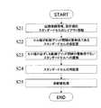
(実施の形態6)
図15は、本発明の実施の形態6におけるスタンダードセルの自動配置配線方法の処理フローを表わしている。(Embodiment 6)
FIG. 15 shows the processing flow of the standard cell automatic placement and routing method according to the sixth embodiment of the present invention.
この自動配置配線方法を実行する自動配置配線装置は、論理回路の接続情報を入力する接続情報入力手段と、設計規約入力手段と、スタンダードセルのレイアウト情報入力手段と、各セル群を接続情報に基づいて配置する配置手段とを備えている。このような構成を有する自動配置配線装置は複数のスタンダードセルを含む状態で論理回路を配置配線する。 An automatic placement and routing apparatus for executing this automatic placement and routing method includes connection information input means for inputting logic circuit connection information, design rule input means, layout information input means for standard cells, and each cell group as connection information. And arranging means for arranging based on. The automatic placement and routing apparatus having such a configuration places and routes a logic circuit in a state including a plurality of standard cells.
まず、予め、複数のスタンダードセルどうしを互いに接続するための論理回路の回路接続情報、自動配置配線を行う際に必要となる設計規約、および各スタンダードセルのレイアウトデータを図示しない記憶装置に格納しておく。ここで記憶装置に格納されるレイアウト情報は、セルC21,C22,C23として、実施の形態5で説明した構造を有するセルのレイアウト情報である。 First, the circuit connection information of logic circuits for connecting a plurality of standard cells to each other, the design rules necessary for automatic placement and routing, and the layout data of each standard cell are stored in a storage device (not shown). Keep it. Here, the layout information stored in the storage device is the layout information of the cells having the structure described in the fifth embodiment as the cells C21, C22, and C23.
そのうえで、自動配置配線装置は、データ読み込み工程S31において、上述した論理回路の回路接続情報、設計規約、および各スタンダードセルのレイアウトデータを記憶装置から読み出す。 In addition, in the data reading step S31, the automatic placement and routing apparatus reads out the above-described logic circuit circuit connection information, design rules, and layout data of each standard cell from the storage device.
次に、自動配置配線装置は、配置工程S32において、回路接続情報に基づいてセルC91,C92,C93を配置する。ここで、セルC91,C92,C93は、図16に示すように、X方向にはセル幅を規定するゲートピッチGxの整数倍のグリッド位置に、Y方向にはY方向の隣接配線グリッド間の中点に位置するように配置される。 Next, the automatic placement and routing apparatus places cells C91, C92, and C93 based on the circuit connection information in the placement step S32. Here, as shown in FIG. 16, the cells C91, C92, and C93 are located at grid positions that are integral multiples of the gate pitch Gx that defines the cell width in the X direction, and between adjacent wiring grids in the Y direction in the Y direction. It is arranged to be located at the midpoint.
その後、自動配置配線装置は、実配線処理工程S33において、配置したセルC91,C92,C93どうしの配線処理を行う。 Thereafter, the automatic placement and routing apparatus performs wiring processing between the placed cells C91, C92, and C93 in the actual wiring processing step S33.
実施の形態6では、配置工程S32で実施するセル配置において、各セルをX方向にはセル幅を規定するゲートピッチGxの整数倍のグリッド位置に配置することで配置面積を小さくして、チップサイズを小さくすることができる。 In the sixth embodiment, in the cell arrangement performed in the arrangement step S32, each cell is arranged at a grid position that is an integral multiple of the gate pitch Gx that defines the cell width in the X direction, thereby reducing the arrangement area. The size can be reduced.
さらには、実施の形態6では、スタンダードセルとして実施の形態1や実施の形態5で説明したスタンダードセルを使用している。これにより、配置されたスタンダードセルC91,C92,C93のゲート電極のパターンはゲート長、ゲート間隔ともに一定となっており、ゲート電極の仕上がり寸法の精度を高くすることができる。このようなゲート電極の仕上がり精度の向上は、スタンダードセルC91,C92,C93内だけでなく、スタンダードセルの間においても得られる。 Furthermore, in the sixth embodiment, the standard cell described in the first or fifth embodiment is used as the standard cell. As a result, the gate electrode patterns of the arranged standard cells C91, C92, and C93 have a constant gate length and gate interval, and the accuracy of the finished dimensions of the gate electrodes can be increased. Such an improvement in the finishing accuracy of the gate electrode can be obtained not only in the standard cells C91, C92, C93 but also between the standard cells.
さらに各スタンダードセル単体で見た場合と、それを隣接して配置した状態とではゲート電極のゲート長、ゲート間隔のパターンが同一となるため、OPCを各スタンダードセル単体で行うことができる。 Furthermore, since the pattern of the gate length and the gate interval of the gate electrode is the same when viewed from each standard cell alone and in a state in which the standard cells are arranged adjacent to each other, OPC can be performed by each standard cell alone.
なお、実施の形態6に示すスタンダードセルの自動配置配線方法は、データ読み込み工程S21、配置工程S22、実配線処理工程S23などをCPUなどにおいて演算処理を行わせることで実現できる。そうすれば、設計者はキーボードなどを使用して設計規約等を記憶装置に入力して記憶させたうえで、設計途中においては、モニター画面などを通じて設計の途中段階のデータの確認や、配線処理後のデータの確認などをすることができる。このようにして本実施形態はハードウェア上で実現することができる。 Note that the automatic placement and routing method for standard cells shown in the sixth embodiment can be realized by causing the data reading step S21, the placement step S22, the actual wiring processing step S23 and the like to perform arithmetic processing in a CPU or the like. Then, the designer inputs the design rules etc. into the storage device using a keyboard and stores them, and in the middle of the design, confirms the data in the middle of the design through the monitor screen etc. You can check the data later. In this way, the present embodiment can be realized on hardware.
このように本発明は、配線長を短く設計できて、チップの小面積化に対して有効である。さらには、電源降下の低減による遅延時間の短縮化、ばらつき削減などにおいて有効である。 Thus, the present invention can be designed to shorten the wiring length and is effective for reducing the chip area. Furthermore, it is effective in shortening the delay time and reducing variation by reducing the power supply drop.
C1〜C3,C11〜C13,C21〜C23,C31〜C33 スタンダードセル
O1〜O3,O11〜O13,O21〜O23,O31〜O33 原点
G ゲート電極LxのX方向グリッド間隔
Ly Y方向グリッド間隔
R21,R22 余分な(無駄な)領域
T 入出力信号を伝達可能な端子
W セル幅
x1〜x13 X方向配線グリッド
y1〜y8 Y方向配線グリッC1-C3, C11-C13, C21-C23, C31-C33 Standard cells O1-O3, O11-O13, O21-O23, O31-O33 Origin G G-direction grid spacing Ly of gate electrodes Lx Y-direction grid spacing R21, R22 Extra (useless) area T Terminal W capable of transmitting input / output signals Cell width x1 to x13 X direction wiring grid y1 to y8 Y direction wiring grid
Claims (33)
Translated fromJapanese前記複数の端子は、自動配置配線で用いられるセルの電源配線に垂直な方向であるY方向に並ぶ配線グリッド上に配置され、かつ前記電源配線に平行な方向であるX方向に沿って長い形状を有する、
ことを特徴とするセル。A cell having a plurality of terminals capable of transmitting an input signal or an output signal and serving as a minimum unit in designing a semiconductor integrated device,
The plurality of terminals are arranged on a wiring grid arranged in the Y direction which is a direction perpendicular to the power supply wiring of a cell used in automatic placement and routing, and have a long shape along the X direction which is parallel to the power supply wiring Having
A cell characterized by that.
ことを特徴とする請求項1記載のセル。The short side dimension of the terminal is a wiring width in automatic placement and routing, and the long side dimension of the terminal is equal to or larger than the wiring grid interval along the X direction and is the minimum wiring interval from the cell width of the cell along the X direction. Less than the deducted length,
The cell according to claim 1.
ことを特徴とする請求項1記載のセル。The short side dimension of the terminal is a wiring width in automatic placement and routing, and the long side dimension of the terminal is equal to or greater than (wiring grid interval along the X direction + the wiring width) and the cell width of the cell along the X direction. Less than or equal to the length minus the minimum wiring spacing,
The cell according to claim 1.
ことを特徴とする請求項1記載のセル。The short side dimension of the terminal is a wiring width in automatic placement and routing, and the long side dimension of the terminal is (wiring grid interval along the X direction + wiring width).
The cell according to claim 1.
ことを特徴とする請求項1記載のセル。The short side dimension of the terminal is a wiring width in automatic placement and routing, and the long side dimension of the terminal is a length obtained by subtracting the minimum wiring interval from the cell width of the cell along the X direction.
The cell according to claim 1.
ことを特徴とする請求項1記載のセル。The cell is a standard cell,
The cell according to claim 1.
ことを特徴とする請求項1記載のセル。The cell is a gate array cell,
The cell according to claim 1.
前記セルを実装する回路基板と、
を備える、
ことを特徴とする半導体集積回路。The cell of claim 1;
A circuit board on which the cell is mounted;
Comprising
A semiconductor integrated circuit.
スタンダードセルライブラリ。A standard cell library for synthesizing a functional macro layout, the library including standard cells having a cell width different from an integral multiple of a wiring grid interval;
Standard cell library.
前記ゲート電極の幾つかが有するゲートピッチは、前記スタンダードセルの電源配線に平行なX方向に沿って設定された前記配線グリッド間隔とは異なる値に設定されており、
前記スタンダードセルの電源配線に平行なX方向に沿うセル幅は、前記X方向に沿う前記配線グリッド間隔とは異なる値に設定された前記ゲート電極のゲートピッチのうちの最小値の整数倍に設定されている、
ことを特徴とする請求項9記載のスタンダードセルライブラリ。The standard cell includes a plurality of gate electrodes,
The gate pitch of some of the gate electrodes is set to a value different from the wiring grid interval set along the X direction parallel to the power supply wiring of the standard cell,
The cell width along the X direction parallel to the power supply wiring of the standard cell is set to an integral multiple of the minimum value of the gate pitches of the gate electrodes set to a value different from the wiring grid interval along the X direction. Being
The standard cell library according to claim 9.
少なくとも一つのスタンダードセルのセル原点のY座標を、自動配置配線での隣接配線グリッド間の中点または配線グリッド上に配置し、
前記スタンダードセルのセル原点のX座標を、前記隣接配線グリッド間の中点または前記配線グリッド上とは相違する位置に配置する、
ことを特徴とするスタンダードセル配置方法。A design method that synthesizes a functional macro layout using standard cells.
Place the Y coordinate of the cell origin of at least one standard cell on the midpoint between adjacent wiring grids in automatic placement and routing or on the wiring grid,
The X coordinate of the cell origin of the standard cell is arranged at a midpoint between the adjacent wiring grids or a position different from the wiring grid.
A standard cell arrangement method characterized by that.
ことを特徴とする請求項11記載のスタンダードセル配置方法。The cell of claim 1 is used as the standard cell.
12. The standard cell arrangement method according to claim 11, wherein
前記スタンダードセルを仮配置したうえで、
仮配置した前記スタンダードセルのセル原点のY座標が、自動配置配線での隣接配線グリッド間の中点または配線グリッド上に位置するとともに、前記セル原点のX座標が、前記隣接配線グリッド間の中点または前記配線グリッド上に位置する場合には、
前記セル原点を、当該セル原点を有する前記スタンダードセルが隣接スタンダードセルに当接する位置に移動させる、
ことを特徴とするスタンダードセル配置方法。A design method that synthesizes a functional macro layout using standard cells.
After temporarily placing the standard cell,
The Y coordinate of the cell origin of the temporarily placed standard cell is located on the midpoint or wiring grid between adjacent wiring grids in automatic placement and routing, and the X coordinate of the cell origin is between the adjacent wiring grids. If located on a point or the wiring grid,
Moving the cell origin to a position where the standard cell having the cell origin contacts an adjacent standard cell;
A standard cell arrangement method characterized by that.
ことを特徴とする請求項13記載のスタンダードセル配置方法。The standard cell of claim 1 is used as the standard cell.
14. The standard cell arrangement method according to claim 13, wherein
前記スタンダードセルを仮配置したうえで、
仮配置した前記スタンダードセルに、各セル幅が自動配置配線での配線グリッド間隔の整数倍である第1のセル群が含まれる場合には、
前記第1のセル群を、セル幅が必ずしも前記配線グリッド間隔の整数倍でない第2のセル群に置換する、
ことを特徴とするスタンダードセル配置方法。A design method that synthesizes a functional macro layout using standard cells.
After temporarily placing the standard cell,
In the case where the first cell group in which each cell width is an integer multiple of the wiring grid interval in the automatic placement and routing is included in the temporarily arranged standard cells,
Replacing the first cell group with a second cell group whose cell width is not necessarily an integer multiple of the wiring grid spacing;
A standard cell arrangement method characterized by that.
ことを特徴とする請求項15記載のスタンダードセル配置方法。As the second cell group, those included in the cell library of claim 9 are used.
The standard cell arrangement method according to claim 15, wherein:
配置した前記スタンダードセルを、当該スタンダードセルの接続情報に従って仮配線するステップと、
前記スタンダードセルに含まれる端子レイアウトのうち配線に不要な部分を削除するステップと、
を含む、
ことを特徴とするスタンダードセル配置方法。Placing the standard cell of claim 5;
Temporary wiring the arranged standard cells according to the connection information of the standard cells;
Deleting a portion of the terminal layout included in the standard cell that is unnecessary for wiring;
including,
A standard cell arrangement method characterized by that.
当該スタンダードセルの電源配線に平行なX方向に沿った当該スタンダードセルのセル幅は、X方向に並ぶ配線グリット間隔とは異なる数値の整数倍である、
ことを特徴とするスタンダードセル。A standard cell having a plurality of gate electrodes,
The cell width of the standard cell along the X direction parallel to the power supply wiring of the standard cell is an integer multiple of a numerical value different from the wiring grid interval arranged in the X direction.
Standard cell characterized by that.
前記ゲート電極の幾つかが有するゲートピッチは、前記スタンダードセルの電源配線に平行なX方向に沿って設定された前記配線グリッド間隔とは異なる値に設定されており、
前記スタンダードセルの電源配線に平行なX方向に沿ったセル幅は、前記X方向に沿って設定された前記配線グリッド間隔とは異なる値に設定された前記ゲート電極のゲートピッチのうちの最小値の整数倍に設定されている、
ことを特徴とするスタンダードセル。A standard cell having a plurality of gate electrodes,
The gate pitch of some of the gate electrodes is set to a value different from the wiring grid interval set along the X direction parallel to the power supply wiring of the standard cell,
The cell width along the X direction parallel to the power supply wiring of the standard cell has a minimum value among the gate pitches of the gate electrodes set to a value different from the wiring grid interval set along the X direction. Is set to an integer multiple of
Standard cell characterized by that.
ことを特徴とする請求項19記載のスタンダードセル。The gate electrode includes a dummy gate electrode,
20. The standard cell according to claim 19, wherein:
ことを特徴とする請求項19記載のスタンダードセル。The gate pitches are all equal,
20. The standard cell according to claim 19, wherein:
ことを特徴とする請求項19記載のスタンダードセル。At least one gate length of the gate electrode is different from the gate length of the other gate electrode;
20. The standard cell according to claim 19, wherein:
前記端子は、自動配置配線で用いられるセルの電源配線に垂直な方向であるY方向に並ぶ配線グリッド上に配置され、かつ前記電源配線に平行な方向であるX方向に沿って長い形状を有する、
ことを特徴とする請求項19記載のスタンダードセル。It further comprises a plurality of terminals capable of transmitting input signals or output signals,
The terminals are arranged on a wiring grid arranged in the Y direction which is a direction perpendicular to the power supply wiring of a cell used in automatic placement and wiring, and have a long shape along the X direction which is parallel to the power supply wiring. ,
20. The standard cell according to claim 19, wherein:
ことを特徴とする請求項23記載のスタンダードセル。The short side dimension of the terminal is a wiring width in automatic placement and routing, and the long side dimension of the terminal is greater than or equal to the wiring grid interval along the X direction and is determined from the cell width of the standard cell along the X direction. Less than the length minus the minimum spacing,
24. The standard cell according to claim 23.
ことを特徴とする請求項23記載のスタンダードセル。The short side dimension of the terminal is a wiring width in automatic placement and routing, and the long side dimension of the terminal is equal to or greater than (wiring grid interval along the X direction + wiring width) and the standard cell along the X direction. Less than the length of the cell width minus the minimum wiring spacing,
24. The standard cell according to claim 23.
ことを特徴とする請求項23記載のスタンダードセル。The short side dimension of the terminal is a wiring width in automatic placement and routing, and the long side dimension of the terminal is (X-direction wiring grid interval + wiring width).
24. The standard cell according to claim 23.
ことを特徴とする請求項23記載のスタンダードセル。The short side dimension of the terminal is a wiring width in automatic placement and routing, and the long side dimension of the terminal is a length obtained by subtracting a minimum wiring interval from the cell width of the standard cell along the X direction.
24. The standard cell according to claim 23.
ことを特徴とするスタンダードセルライブラリ。Including the standard cell of claim 19,
Standard cell library characterized by this.
前記スタンダードセルを実装する回路基板と、
を備える、
ことを特徴とする半導体集積回路。The standard cell of claim 19;
A circuit board on which the standard cell is mounted;
Comprising
A semiconductor integrated circuit.
少なくとも一つのスタンダードセルのセル原点のY座標を、自動配置配線での隣接グリッド間の中点または配線グリッド上に配置し、
前記スタンダードセルのセル原点のX座標を、前記隣接グリッドとは異なるゲートピッチグリッドの中点またはゲートピッチグリッド上に配置する、
ことを特徴とするスタンダードセル配置方法。A design method that synthesizes a functional macro layout using standard cells.
Place the Y coordinate of the cell origin of at least one standard cell on the midpoint between adjacent grids in automatic placement and routing or on the wiring grid,
The X coordinate of the cell origin of the standard cell is arranged on the middle point of the gate pitch grid different from the adjacent grid or on the gate pitch grid.
A standard cell arrangement method characterized by that.
ことを特徴とする請求項30記載のスタンダードセル配置方法。The standard cell according to claim 19 is used as the standard cell.
31. The standard cell arrangement method according to claim 30, wherein:
前記記憶装置から設計対象とするスタンダードセルに関する前記情報を読み出すステップと、
読み出した前記情報に基づいて前記スタンダードセルを配置するステップと、
配置した前記スタンダードセルを実配線するステップと、
を含み、
これらのステップを演算回路で実施する、
ことを特徴とするスタンダードセル配置方法。Storing logic circuit connection information, standard cell layout information, and standard cell design rule information in a storage device;
Reading the information about the standard cell to be designed from the storage device;
Placing the standard cell based on the read information;
A step of actually wiring the arranged standard cells;
Including
Perform these steps in the arithmetic circuit,
A standard cell arrangement method characterized by that.
ことを特徴とする請求項32のスタンダードセル配置方法。The standard cell according to claim 19 is used as the standard cell.
The standard cell arrangement method according to claim 32, wherein:
Priority Applications (3)
| Application Number | Priority Date | Filing Date | Title |
|---|---|---|---|
| JP2005353654AJP2007043049A (en) | 2004-12-20 | 2005-12-07 | Cell, standard cell, standard cell arrangement method, standard cell library, and semiconductor integrated circuit |
| US11/305,191US7503026B2 (en) | 2004-12-20 | 2005-12-19 | Cell, standard cell, standard cell library, a placement method using standard cell, and a semiconductor integrated circuit |
| US12/359,615US20090138840A1 (en) | 2004-12-20 | 2009-01-26 | Cell, standard cell, standard cell library, a placement method using standard cell, and a semiconductor integrated circuit |
Applications Claiming Priority (3)
| Application Number | Priority Date | Filing Date | Title |
|---|---|---|---|
| JP2004367717 | 2004-12-20 | ||
| JP2005191434 | 2005-06-30 | ||
| JP2005353654AJP2007043049A (en) | 2004-12-20 | 2005-12-07 | Cell, standard cell, standard cell arrangement method, standard cell library, and semiconductor integrated circuit |
Publications (1)
| Publication Number | Publication Date |
|---|---|
| JP2007043049Atrue JP2007043049A (en) | 2007-02-15 |
Family
ID=36597651
Family Applications (1)
| Application Number | Title | Priority Date | Filing Date |
|---|---|---|---|
| JP2005353654APendingJP2007043049A (en) | 2004-12-20 | 2005-12-07 | Cell, standard cell, standard cell arrangement method, standard cell library, and semiconductor integrated circuit |
Country Status (2)
| Country | Link |
|---|---|
| US (2) | US7503026B2 (en) |
| JP (1) | JP2007043049A (en) |
Cited By (25)
| Publication number | Priority date | Publication date | Assignee | Title |
|---|---|---|---|---|
| JP2012505526A (en)* | 2008-07-16 | 2012-03-01 | テラ イノヴェイションズ インコーポレイテッド | Method and implementation of cell phase matching and placement in a dynamic array architecture |
| US8426978B2 (en) | 2009-02-17 | 2013-04-23 | Panasonic Corporation | Semiconductor device including a first wiring having a bending portion and a via including the bending portion |
| US8816402B2 (en) | 2008-03-13 | 2014-08-26 | Tela Innovations, Inc. | Integrated circuit including cross-coupled transistors having gate electrodes formed within gate level feature layout channels with gate level feature layout channel including single transistor |
| US8823062B2 (en) | 2006-03-09 | 2014-09-02 | Tela Innovations, Inc. | Integrated circuit with offset line end spacings in linear gate electrode level |
| US8839175B2 (en) | 2006-03-09 | 2014-09-16 | Tela Innovations, Inc. | Scalable meta-data objects |
| JP2014220498A (en)* | 2013-05-02 | 2014-11-20 | 台湾積體電路製造股▲ふん▼有限公司Taiwan Semiconductor Manufacturing Company,Ltd. | Standard cell having cell height which is non-integer multiple of nominal minimum pitch |
| US8951916B2 (en) | 2007-12-13 | 2015-02-10 | Tela Innovations, Inc. | Super-self-aligned contacts and method for making the same |
| US9009641B2 (en) | 2006-03-09 | 2015-04-14 | Tela Innovations, Inc. | Circuits with linear finfet structures |
| US9035359B2 (en) | 2006-03-09 | 2015-05-19 | Tela Innovations, Inc. | Semiconductor chip including region including linear-shaped conductive structures forming gate electrodes and having electrical connection areas arranged relative to inner region between transistors of different types and associated methods |
| US9122832B2 (en) | 2008-08-01 | 2015-09-01 | Tela Innovations, Inc. | Methods for controlling microloading variation in semiconductor wafer layout and fabrication |
| US9159627B2 (en) | 2010-11-12 | 2015-10-13 | Tela Innovations, Inc. | Methods for linewidth modification and apparatus implementing the same |
| US9202779B2 (en) | 2008-01-31 | 2015-12-01 | Tela Innovations, Inc. | Enforcement of semiconductor structure regularity for localized transistors and interconnect |
| US9230910B2 (en) | 2006-03-09 | 2016-01-05 | Tela Innovations, Inc. | Oversized contacts and vias in layout defined by linearly constrained topology |
| US9240413B2 (en) | 2006-03-09 | 2016-01-19 | Tela Innovations, Inc. | Methods, structures, and designs for self-aligning local interconnects used in integrated circuits |
| US9269702B2 (en) | 2009-10-13 | 2016-02-23 | Tela Innovations, Inc. | Methods for cell boundary encroachment and layouts implementing the same |
| US9336344B2 (en) | 2006-03-09 | 2016-05-10 | Tela Innovations, Inc. | Coarse grid design methods and structures |
| US9390215B2 (en) | 2008-03-27 | 2016-07-12 | Tela Innovations, Inc. | Methods for multi-wire routing and apparatus implementing same |
| JP2016225648A (en)* | 2007-08-02 | 2016-12-28 | テラ イノヴェイションズ インク | Integrated circuit device |
| US9563733B2 (en) | 2009-05-06 | 2017-02-07 | Tela Innovations, Inc. | Cell circuit and layout with linear finfet structures |
| US9633987B2 (en) | 2007-03-05 | 2017-04-25 | Tela Innovations, Inc. | Integrated circuit cell library for multiple patterning |
| US9673825B2 (en) | 2006-03-09 | 2017-06-06 | Tela Innovations, Inc. | Circuitry and layouts for XOR and XNOR logic |
| WO2017145906A1 (en)* | 2016-02-25 | 2017-08-31 | 株式会社ソシオネクスト | Semiconductor integrated circuit device |
| US9754878B2 (en) | 2006-03-09 | 2017-09-05 | Tela Innovations, Inc. | Semiconductor chip including a chip level based on a layout that includes both regular and irregular wires |
| US10410917B2 (en) | 2016-03-03 | 2019-09-10 | Samsung Electronics Co., Ltd. | Semiconductor device including standard cell and electronic design automation method thereof |
| KR20220130681A (en)* | 2021-03-17 | 2022-09-27 | 창신 메모리 테크놀로지즈 아이엔씨 | Integrated circuit and method of arrangement thereof |
Families Citing this family (36)
| Publication number | Priority date | Publication date | Assignee | Title |
|---|---|---|---|---|
| US20070101279A1 (en)* | 2005-10-27 | 2007-05-03 | Chaudhri Imran A | Selection of user interface elements for unified display in a display environment |
| JP2008021001A (en)* | 2006-07-11 | 2008-01-31 | Matsushita Electric Ind Co Ltd | Pattern correction device, pattern optimization device, and integrated circuit design device |
| US7577933B1 (en)* | 2006-11-17 | 2009-08-18 | Sun Microsystems, Inc. | Timing driven pin assignment |
| JP2008235350A (en)* | 2007-03-16 | 2008-10-02 | Matsushita Electric Ind Co Ltd | Semiconductor integrated circuit |
| US8037441B2 (en)* | 2007-09-25 | 2011-10-11 | International Business Machines Corporation | Gridded-router based wiring on a non-gridded library |
| JP4448535B2 (en)* | 2007-12-18 | 2010-04-14 | 株式会社 日立ディスプレイズ | Display device |
| US8004014B2 (en) | 2008-07-04 | 2011-08-23 | Panasonic Corporation | Semiconductor integrated circuit device having metal interconnect regions placed symmetrically with respect to a cell boundary |
| US20100057473A1 (en)* | 2008-08-26 | 2010-03-04 | Hongwei Kong | Method and system for dual voice path processing in an audio codec |
| US8600166B2 (en)* | 2009-11-06 | 2013-12-03 | Sony Corporation | Real time hand tracking, pose classification and interface control |
| US8495551B2 (en)* | 2009-12-17 | 2013-07-23 | International Business Machines Corporation | Shaping ports in integrated circuit design |
| US9646958B2 (en)* | 2010-03-17 | 2017-05-09 | Taiwan Semiconductor Manufacturing Company, Ltd. | Integrated circuits including dummy structures and methods of forming the same |
| US8370786B1 (en)* | 2010-05-28 | 2013-02-05 | Golden Gate Technology, Inc. | Methods and software for placement improvement based on global routing |
| US8451026B2 (en)* | 2011-05-13 | 2013-05-28 | Arm Limited | Integrated circuit, method of generating a layout of an integrated circuit using standard cells, and a standard cell library providing such standard cells |
| JP2013030602A (en)* | 2011-07-28 | 2013-02-07 | Panasonic Corp | Semiconductor integrated circuit device |
| US20130320451A1 (en) | 2012-06-01 | 2013-12-05 | Taiwan Semiconductor Manufacturing Company, Ltd., ("Tsmc") | Semiconductor device having non-orthogonal element |
| CN103838895B (en)* | 2012-11-26 | 2017-08-11 | 北京华大九天软件有限公司 | A kind of narrow frame wiring implementation method wing wiring in flat-panel monitor design |
| US9501600B2 (en) | 2013-05-02 | 2016-11-22 | Taiwan Semiconductor Manufacturing Company, Ltd. | Standard cells for predetermined function having different types of layout |
| US9811626B2 (en)* | 2014-09-18 | 2017-11-07 | Samsung Electronics Co., Ltd. | Method of designing layout of semiconductor device |
| US9767248B2 (en) | 2014-09-18 | 2017-09-19 | Samsung Electronics, Co., Ltd. | Semiconductor having cross coupled structure and layout verification method thereof |
| US9704862B2 (en) | 2014-09-18 | 2017-07-11 | Samsung Electronics Co., Ltd. | Semiconductor devices and methods for manufacturing the same |
| US10026661B2 (en) | 2014-09-18 | 2018-07-17 | Samsung Electronics Co., Ltd. | Semiconductor device for testing large number of devices and composing method and test method thereof |
| US10095825B2 (en) | 2014-09-18 | 2018-10-09 | Samsung Electronics Co., Ltd. | Computer based system for verifying layout of semiconductor device and layout verify method thereof |
| KR102423878B1 (en)* | 2014-09-18 | 2022-07-22 | 삼성전자주식회사 | Semiconductor device for testing a large number of devices and composing method and test method thereof |
| KR102321605B1 (en) | 2015-04-09 | 2021-11-08 | 삼성전자주식회사 | Method for designing layout of semiconductor device and method for manufacturing semiconductor device using the same |
| US9698056B2 (en)* | 2015-04-09 | 2017-07-04 | Samsung Electronics., Ltd. | Method for designing layout of semiconductor device and method for manufacturing semiconductor device using the same |
| US10380307B1 (en)* | 2016-03-30 | 2019-08-13 | Silicon Technologies, Inc. | Analog design tool, cell set, and related methods, systems and equipment |
| US10605859B2 (en)* | 2016-09-14 | 2020-03-31 | Qualcomm Incorporated | Visible alignment markers/landmarks for CAD-to-silicon backside image alignment |
| KR102678555B1 (en)* | 2016-10-05 | 2024-06-26 | 삼성전자주식회사 | Integrated circuit including modified cell and method of designing the same |
| KR102699046B1 (en)* | 2016-12-15 | 2024-08-27 | 삼성전자주식회사 | Integrated circuit having vertical transistor and semiconductor device including the same |
| KR102373540B1 (en)* | 2018-04-19 | 2022-03-11 | 삼성전자주식회사 | Integrated circuit including standard cell and method and system for fabricating the same |
| CN109345607B (en)* | 2018-10-11 | 2023-02-28 | 广州前实网络科技有限公司 | Method for automatically marking EPC picture |
| KR102720606B1 (en) | 2019-01-18 | 2024-10-21 | 삼성전자주식회사 | Method for fabricating semiconductor device |
| KR102843610B1 (en) | 2019-10-08 | 2025-08-06 | 삼성전자주식회사 | Semiconductor device, layout design method for the same and method for fabricating the same |
| DE102020132921A1 (en)* | 2020-04-30 | 2021-11-04 | Taiwan Semiconductor Manufacturing Co., Ltd. | SEMICONDUCTOR DEVICE WITH STEPPED GATE TUBE SIZE PROFILE AND METHOD OF MANUFACTURING THEREOF |
| US11842994B2 (en)* | 2020-04-30 | 2023-12-12 | Taiwan Semiconductor Manufacturing Company, Ltd | Semiconductor device having staggered gate-stub-size profile and method of manufacturing same |
| CN115249002A (en)* | 2021-04-26 | 2022-10-28 | 联华电子股份有限公司 | IC Layout |
Citations (6)
| Publication number | Priority date | Publication date | Assignee | Title |
|---|---|---|---|---|
| JPS63224237A (en)* | 1987-03-12 | 1988-09-19 | Toshiba Corp | Automatic generation method of functional blocks for semiconductor integrated circuit devices |
| JPH05136356A (en)* | 1991-11-13 | 1993-06-01 | Nec Corp | Semiconductor integrated circuit |
| JPH0677323A (en)* | 1992-08-25 | 1994-03-18 | Nec Corp | Automatic layout system |
| JPH0722598A (en)* | 1993-07-01 | 1995-01-24 | Mitsubishi Denki Eng Kk | Semiconductor integrated circuit |
| JP2001015602A (en)* | 1999-06-28 | 2001-01-19 | Nec Ic Microcomput Syst Ltd | Standard cell, standard cell column, standard cell placement and routing device and placement and routing method |
| JP2004342757A (en)* | 2003-05-14 | 2004-12-02 | Toshiba Corp | Semiconductor integrated circuit and design method thereof |
Family Cites Families (19)
| Publication number | Priority date | Publication date | Assignee | Title |
|---|---|---|---|---|
| JPS55115353A (en)* | 1979-02-27 | 1980-09-05 | Fujitsu Ltd | Cell rotatable by 90 |
| JPH0691156B2 (en) | 1984-08-09 | 1994-11-14 | 日本電気株式会社 | Method for manufacturing semiconductor integrated circuit |
| JPS6247148A (en) | 1985-08-27 | 1987-02-28 | Toshiba Corp | Semiconductor integrated circuit device |
| US5168342A (en)* | 1989-01-30 | 1992-12-01 | Hitachi, Ltd. | Semiconductor integrated circuit device and manufacturing method of the same |
| JP2810181B2 (en) | 1990-01-08 | 1998-10-15 | 株式会社日立製作所 | Cell layout method |
| JP3266644B2 (en)* | 1991-04-08 | 2002-03-18 | テキサス インスツルメンツ インコーポレイテツド | Gate array device |
| JPH1041398A (en) | 1996-04-10 | 1998-02-13 | Toshiba Corp | Semiconductor integrated circuit device |
| US6084256A (en)* | 1996-04-10 | 2000-07-04 | Kabushiki Kaisha Toshiba | Semiconductor integrated circuit device |
| JPH09289251A (en) | 1996-04-23 | 1997-11-04 | Matsushita Electric Ind Co Ltd | Layout structure of semiconductor integrated circuit and its verification method |
| JP3311244B2 (en)* | 1996-07-15 | 2002-08-05 | 株式会社東芝 | Basic cell library and method of forming the same |
| US5977574A (en)* | 1997-03-28 | 1999-11-02 | Lsi Logic Corporation | High density gate array cell architecture with sharing of well taps between cells |
| JP3160586B2 (en)* | 1999-04-27 | 2001-04-25 | 松下電子工業株式会社 | CMOS inverter and standard cell using the same |
| US6207479B1 (en)* | 1999-06-14 | 2001-03-27 | Taiwan Semiconductor Manufacturing Co., Ltd. | Place and route method for integrated circuit design |
| US6525350B1 (en)* | 1999-07-16 | 2003-02-25 | Kawasaki Steel Corporation | Semiconductor integrated circuit basic cell semiconductor integrated circuit using the same |
| US6445214B2 (en)* | 2000-02-03 | 2002-09-03 | Hitachi, Ltd. | Semiconductor integrated circuit |
| JP4794030B2 (en)* | 2000-07-10 | 2011-10-12 | ルネサスエレクトロニクス株式会社 | Semiconductor device |
| US6567967B2 (en)* | 2000-09-06 | 2003-05-20 | Monterey Design Systems, Inc. | Method for designing large standard-cell base integrated circuits |
| JP3996735B2 (en)* | 2000-11-30 | 2007-10-24 | 株式会社ルネサステクノロジ | Semiconductor device |
| JP4416384B2 (en)* | 2002-07-19 | 2010-02-17 | 株式会社ルネサステクノロジ | Semiconductor integrated circuit |
- 2005
- 2005-12-07JPJP2005353654Apatent/JP2007043049A/enactivePending
- 2005-12-19USUS11/305,191patent/US7503026B2/enactiveActive
- 2009
- 2009-01-26USUS12/359,615patent/US20090138840A1/ennot_activeAbandoned
Patent Citations (6)
| Publication number | Priority date | Publication date | Assignee | Title |
|---|---|---|---|---|
| JPS63224237A (en)* | 1987-03-12 | 1988-09-19 | Toshiba Corp | Automatic generation method of functional blocks for semiconductor integrated circuit devices |
| JPH05136356A (en)* | 1991-11-13 | 1993-06-01 | Nec Corp | Semiconductor integrated circuit |
| JPH0677323A (en)* | 1992-08-25 | 1994-03-18 | Nec Corp | Automatic layout system |
| JPH0722598A (en)* | 1993-07-01 | 1995-01-24 | Mitsubishi Denki Eng Kk | Semiconductor integrated circuit |
| JP2001015602A (en)* | 1999-06-28 | 2001-01-19 | Nec Ic Microcomput Syst Ltd | Standard cell, standard cell column, standard cell placement and routing device and placement and routing method |
| JP2004342757A (en)* | 2003-05-14 | 2004-12-02 | Toshiba Corp | Semiconductor integrated circuit and design method thereof |
Cited By (91)
| Publication number | Priority date | Publication date | Assignee | Title |
|---|---|---|---|---|
| US9917056B2 (en) | 2006-03-09 | 2018-03-13 | Tela Innovations, Inc. | Coarse grid design methods and structures |
| US9754878B2 (en) | 2006-03-09 | 2017-09-05 | Tela Innovations, Inc. | Semiconductor chip including a chip level based on a layout that includes both regular and irregular wires |
| US10230377B2 (en) | 2006-03-09 | 2019-03-12 | Tela Innovations, Inc. | Circuitry and layouts for XOR and XNOR logic |
| US8823062B2 (en) | 2006-03-09 | 2014-09-02 | Tela Innovations, Inc. | Integrated circuit with offset line end spacings in linear gate electrode level |
| US10217763B2 (en) | 2006-03-09 | 2019-02-26 | Tela Innovations, Inc. | Semiconductor chip having region including gate electrode features of rectangular shape on gate horizontal grid and first-metal structures of rectangular shape on at least eight first-metal gridlines of first-metal vertical grid |
| US10186523B2 (en) | 2006-03-09 | 2019-01-22 | Tela Innovations, Inc. | Semiconductor chip having region including gate electrode features formed in part from rectangular layout shapes on gate horizontal grid and first-metal structures formed in part from rectangular layout shapes on at least eight first-metal gridlines of first-metal vertical grid |
| US8839175B2 (en) | 2006-03-09 | 2014-09-16 | Tela Innovations, Inc. | Scalable meta-data objects |
| US10141335B2 (en) | 2006-03-09 | 2018-11-27 | Tela Innovations, Inc. | Semiconductor CIP including region having rectangular-shaped gate structures and first metal structures |
| US10141334B2 (en) | 2006-03-09 | 2018-11-27 | Tela Innovations, Inc. | Semiconductor chip including region having rectangular-shaped gate structures and first-metal structures |
| US9336344B2 (en) | 2006-03-09 | 2016-05-10 | Tela Innovations, Inc. | Coarse grid design methods and structures |
| US9425145B2 (en) | 2006-03-09 | 2016-08-23 | Tela Innovations, Inc. | Oversized contacts and vias in layout defined by linearly constrained topology |
| US9905576B2 (en) | 2006-03-09 | 2018-02-27 | Tela Innovations, Inc. | Semiconductor chip including region having rectangular-shaped gate structures and first metal structures |
| US9859277B2 (en) | 2006-03-09 | 2018-01-02 | Tela Innovations, Inc. | Methods, structures, and designs for self-aligning local interconnects used in integrated circuits |
| US9425273B2 (en) | 2006-03-09 | 2016-08-23 | Tela Innovations, Inc. | Semiconductor chip including integrated circuit including at least five gate level conductive structures having particular spatial and electrical relationship and method for manufacturing the same |
| US9741719B2 (en) | 2006-03-09 | 2017-08-22 | Tela Innovations, Inc. | Methods, structures, and designs for self-aligning local interconnects used in integrated circuits |
| US9711495B2 (en) | 2006-03-09 | 2017-07-18 | Tela Innovations, Inc. | Oversized contacts and vias in layout defined by linearly constrained topology |
| US8921897B2 (en) | 2006-03-09 | 2014-12-30 | Tela Innovations, Inc. | Integrated circuit with gate electrode conductive structures having offset ends |
| US8921896B2 (en) | 2006-03-09 | 2014-12-30 | Tela Innovations, Inc. | Integrated circuit including linear gate electrode structures having different extension distances beyond contact |
| US8946781B2 (en) | 2006-03-09 | 2015-02-03 | Tela Innovations, Inc. | Integrated circuit including gate electrode conductive structures with different extension distances beyond contact |
| US8952425B2 (en) | 2006-03-09 | 2015-02-10 | Tela Innovations, Inc. | Integrated circuit including at least four linear-shaped conductive structures having extending portions of different length |
| US9673825B2 (en) | 2006-03-09 | 2017-06-06 | Tela Innovations, Inc. | Circuitry and layouts for XOR and XNOR logic |
| US9240413B2 (en) | 2006-03-09 | 2016-01-19 | Tela Innovations, Inc. | Methods, structures, and designs for self-aligning local interconnects used in integrated circuits |
| US9009641B2 (en) | 2006-03-09 | 2015-04-14 | Tela Innovations, Inc. | Circuits with linear finfet structures |
| US9035359B2 (en) | 2006-03-09 | 2015-05-19 | Tela Innovations, Inc. | Semiconductor chip including region including linear-shaped conductive structures forming gate electrodes and having electrical connection areas arranged relative to inner region between transistors of different types and associated methods |
| US9230910B2 (en) | 2006-03-09 | 2016-01-05 | Tela Innovations, Inc. | Oversized contacts and vias in layout defined by linearly constrained topology |
| US9425272B2 (en) | 2006-03-09 | 2016-08-23 | Tela Innovations, Inc. | Semiconductor chip including integrated circuit including four transistors of first transistor type and four transistors of second transistor type with electrical connections between various transistors and methods for manufacturing the same |
| US9589091B2 (en) | 2006-03-09 | 2017-03-07 | Tela Innovations, Inc. | Scalable meta-data objects |
| US9443947B2 (en) | 2006-03-09 | 2016-09-13 | Tela Innovations, Inc. | Semiconductor chip including region having integrated circuit transistor gate electrodes formed by various conductive structures of specified shape and position and method for manufacturing the same |
| US10074640B2 (en) | 2007-03-05 | 2018-09-11 | Tela Innovations, Inc. | Integrated circuit cell library for multiple patterning |
| US9633987B2 (en) | 2007-03-05 | 2017-04-25 | Tela Innovations, Inc. | Integrated circuit cell library for multiple patterning |
| US9424387B2 (en) | 2007-03-07 | 2016-08-23 | Tela Innovations, Inc. | Methods for cell phasing and placement in dynamic array architecture and implementation of the same |
| US9595515B2 (en) | 2007-03-07 | 2017-03-14 | Tela Innovations, Inc. | Semiconductor chip including integrated circuit defined within dynamic array section |
| US8966424B2 (en) | 2007-03-07 | 2015-02-24 | Tela Innovations, Inc. | Methods for cell phasing and placement in dynamic array architecture and implementation of the same |
| US9910950B2 (en) | 2007-03-07 | 2018-03-06 | Tela Innovations, Inc. | Methods for cell phasing and placement in dynamic array architecture and implementation of the same |
| JP2018050072A (en)* | 2007-08-02 | 2018-03-29 | テラ イノヴェイションズ インク | Integrated circuit device |
| JP2016225648A (en)* | 2007-08-02 | 2016-12-28 | テラ イノヴェイションズ インク | Integrated circuit device |
| US10734383B2 (en) | 2007-10-26 | 2020-08-04 | Tela Innovations, Inc. | Methods, structures, and designs for self-aligning local interconnects used in integrated circuits |
| US9818747B2 (en) | 2007-12-13 | 2017-11-14 | Tela Innovations, Inc. | Super-self-aligned contacts and method for making the same |
| US8951916B2 (en) | 2007-12-13 | 2015-02-10 | Tela Innovations, Inc. | Super-self-aligned contacts and method for making the same |
| US9281371B2 (en) | 2007-12-13 | 2016-03-08 | Tela Innovations, Inc. | Super-self-aligned contacts and method for making the same |
| US10461081B2 (en) | 2007-12-13 | 2019-10-29 | Tel Innovations, Inc. | Super-self-aligned contacts and method for making the same |
| US9530734B2 (en) | 2008-01-31 | 2016-12-27 | Tela Innovations, Inc. | Enforcement of semiconductor structure regularity for localized transistors and interconnect |
| US9202779B2 (en) | 2008-01-31 | 2015-12-01 | Tela Innovations, Inc. | Enforcement of semiconductor structure regularity for localized transistors and interconnect |
| US9117050B2 (en) | 2008-03-13 | 2015-08-25 | Tela Innovations, Inc. | Integrated circuit including cross-coupled transistors having gate electrodes formed within gate level feature layout channels with gate contact position and offset specifications |
| US8835989B2 (en) | 2008-03-13 | 2014-09-16 | Tela Innovations, Inc. | Integrated circuit including cross-coupled transistors having gate electrodes formed within gate level feature layout channels with gate electrode placement specifications |
| US9213792B2 (en) | 2008-03-13 | 2015-12-15 | Tela Innovations, Inc. | Semiconductor chip including digital logic circuit including at least six transistors with some transistors forming cross-coupled transistor configuration and associated methods |
| US8853793B2 (en) | 2008-03-13 | 2014-10-07 | Tela Innovations, Inc. | Integrated circuit including gate electrode level region including cross-coupled transistors having gate contacts located over inner portion of gate electrode level region and offset gate level feature line ends |
| US10658385B2 (en) | 2008-03-13 | 2020-05-19 | Tela Innovations, Inc. | Cross-coupled transistor circuit defined on four gate electrode tracks |
| US9536899B2 (en) | 2008-03-13 | 2017-01-03 | Tela Innovations, Inc. | Semiconductor chip including integrated circuit having cross-coupled transistor configuration and method for manufacturing the same |
| US9208279B2 (en) | 2008-03-13 | 2015-12-08 | Tela Innovations, Inc. | Semiconductor chip including digital logic circuit including linear-shaped conductive structures having electrical connection areas located within inner region between transistors of different type and associated methods |
| US10727252B2 (en) | 2008-03-13 | 2020-07-28 | Tela Innovations, Inc. | Semiconductor chip including integrated circuit having cross-coupled transistor configuration and method for manufacturing the same |
| US10020321B2 (en) | 2008-03-13 | 2018-07-10 | Tela Innovations, Inc. | Cross-coupled transistor circuit defined on two gate electrode tracks |
| US9081931B2 (en) | 2008-03-13 | 2015-07-14 | Tela Innovations, Inc. | Cross-coupled transistor circuit having diffusion regions of common node on opposing sides of same gate electrode track and gate node connection through single interconnect layer |
| US8816402B2 (en) | 2008-03-13 | 2014-08-26 | Tela Innovations, Inc. | Integrated circuit including cross-coupled transistors having gate electrodes formed within gate level feature layout channels with gate level feature layout channel including single transistor |
| US9245081B2 (en) | 2008-03-13 | 2016-01-26 | Tela Innovations, Inc. | Semiconductor chip including digital logic circuit including at least nine linear-shaped conductive structures collectively forming gate electrodes of at least six transistors with some transistors forming cross-coupled transistor configuration and associated methods |
| US8836045B2 (en) | 2008-03-13 | 2014-09-16 | Tela Innovations, Inc. | Cross-coupled transistor circuit having diffusion regions of common node on opposing sides of same gate electrode track |
| US10651200B2 (en) | 2008-03-13 | 2020-05-12 | Tela Innovations, Inc. | Cross-coupled transistor circuit defined on three gate electrode tracks |
| US8847331B2 (en) | 2008-03-13 | 2014-09-30 | Tela Innovations, Inc. | Semiconductor chip including region having cross-coupled transistor configuration with offset electrical connection areas on gate electrode forming conductive structures and at least two different inner extension distances of gate electrode forming conductive structures |
| US8872283B2 (en) | 2008-03-13 | 2014-10-28 | Tela Innovations, Inc. | Integrated circuit including cross-coupled transistors having gate electrodes formed within gate level feature layout channels with shared diffusion regions on opposite sides of two-transistor-forming gate level feature |
| US8847329B2 (en) | 2008-03-13 | 2014-09-30 | Tela Innovations, Inc. | Cross-coupled transistor circuit defined having diffusion regions of common node on opposing sides of same gate electrode track with at least two non-inner positioned gate contacts |
| US8853794B2 (en) | 2008-03-13 | 2014-10-07 | Tela Innovations, Inc. | Integrated circuit within semiconductor chip including cross-coupled transistor configuration |
| US9871056B2 (en) | 2008-03-13 | 2018-01-16 | Tela Innovations, Inc. | Semiconductor chip including integrated circuit having cross-coupled transistor configuration and method for manufacturing the same |
| US8866197B2 (en) | 2008-03-13 | 2014-10-21 | Tela Innovations, Inc. | Integrated circuit including cross-coupled transistors having gate electrodes formed within gate level feature layout channels with at least two gate electrodes electrically connected to each other through another transistor forming gate level feature |
| US9779200B2 (en) | 2008-03-27 | 2017-10-03 | Tela Innovations, Inc. | Methods for multi-wire routing and apparatus implementing same |
| US9390215B2 (en) | 2008-03-27 | 2016-07-12 | Tela Innovations, Inc. | Methods for multi-wire routing and apparatus implementing same |
| JP2016136650A (en)* | 2008-07-16 | 2016-07-28 | テラ イノヴェイションズ インコーポレイテッド | Method and implementation of cell phase matching and placement in a dynamic array architecture |
| JP2014199934A (en)* | 2008-07-16 | 2014-10-23 | テラ イノヴェイションズ インコーポレイテッド | Method for cell phase matching and placement in dynamic array architecture and implementation of the same |
| JP2012505526A (en)* | 2008-07-16 | 2012-03-01 | テラ イノヴェイションズ インコーポレイテッド | Method and implementation of cell phase matching and placement in a dynamic array architecture |
| JP2017143307A (en)* | 2008-07-16 | 2017-08-17 | テラ イノヴェイションズ インコーポレイテッド | Method for cell phase matching and arrangement in dynamic array architecture and implementation of the same |
| US9122832B2 (en) | 2008-08-01 | 2015-09-01 | Tela Innovations, Inc. | Methods for controlling microloading variation in semiconductor wafer layout and fabrication |
| US8841774B2 (en) | 2009-02-17 | 2014-09-23 | Panasonic Corporation | Semiconductor device including a first wiring having a bending portion a via |
| US8426978B2 (en) | 2009-02-17 | 2013-04-23 | Panasonic Corporation | Semiconductor device including a first wiring having a bending portion and a via including the bending portion |
| US10446536B2 (en) | 2009-05-06 | 2019-10-15 | Tela Innovations, Inc. | Cell circuit and layout with linear finfet structures |
| US9563733B2 (en) | 2009-05-06 | 2017-02-07 | Tela Innovations, Inc. | Cell circuit and layout with linear finfet structures |
| US9269702B2 (en) | 2009-10-13 | 2016-02-23 | Tela Innovations, Inc. | Methods for cell boundary encroachment and layouts implementing the same |
| US9530795B2 (en) | 2009-10-13 | 2016-12-27 | Tela Innovations, Inc. | Methods for cell boundary encroachment and semiconductor devices implementing the same |
| US9704845B2 (en) | 2010-11-12 | 2017-07-11 | Tela Innovations, Inc. | Methods for linewidth modification and apparatus implementing the same |
| US9159627B2 (en) | 2010-11-12 | 2015-10-13 | Tela Innovations, Inc. | Methods for linewidth modification and apparatus implementing the same |
| US10867099B2 (en) | 2013-05-02 | 2020-12-15 | Taiwan Semiconductor Manufacturing Company, Ltd. | System for designing integrated circuit layout and method of making the integrated circuit layout |
| US12153868B2 (en) | 2013-05-02 | 2024-11-26 | Taiwan Semiconductor Manufacturing Company, Ltd. | Integrated circuit having non-integral multiple pitch |
| US9659129B2 (en) | 2013-05-02 | 2017-05-23 | Taiwan Semiconductor Manufacturing Company, Ltd. | Standard cell having cell height being non-integral multiple of nominal minimum pitch |
| JP2016189489A (en)* | 2013-05-02 | 2016-11-04 | 台湾積體電路製造股▲ふん▼有限公司Taiwan Semiconductor Manufacturing Company,Ltd. | Standard cell having cell height which is non-integer multiple of nominal minimum pitch |
| JP2014220498A (en)* | 2013-05-02 | 2014-11-20 | 台湾積體電路製造股▲ふん▼有限公司Taiwan Semiconductor Manufacturing Company,Ltd. | Standard cell having cell height which is non-integer multiple of nominal minimum pitch |
| US10289789B2 (en) | 2013-05-02 | 2019-05-14 | Taiwan Semiconductor Manufacturing Company, Ltd. | System for designing integrated circuit layout and method of making the integrated circuit layout |
| US11544437B2 (en) | 2013-05-02 | 2023-01-03 | Taiwan Semiconductor Manufacturing Company, Ltd. | System for designing integrated circuit layout and method of making the integrated circuit layout |
| JPWO2017145906A1 (en)* | 2016-02-25 | 2018-12-27 | 株式会社ソシオネクスト | Semiconductor integrated circuit device |
| WO2017145906A1 (en)* | 2016-02-25 | 2017-08-31 | 株式会社ソシオネクスト | Semiconductor integrated circuit device |
| US10410917B2 (en) | 2016-03-03 | 2019-09-10 | Samsung Electronics Co., Ltd. | Semiconductor device including standard cell and electronic design automation method thereof |
| KR20220130681A (en)* | 2021-03-17 | 2022-09-27 | 창신 메모리 테크놀로지즈 아이엔씨 | Integrated circuit and method of arrangement thereof |
| JP2023522522A (en)* | 2021-03-17 | 2023-05-31 | チャンシン メモリー テクノロジーズ インコーポレイテッド | Integrated circuit and its layout method |
| KR102813105B1 (en)* | 2021-03-17 | 2025-05-26 | 창신 메모리 테크놀로지즈 아이엔씨 | Integrated circuit and method of arranging the same |
Also Published As
| Publication number | Publication date |
|---|---|
| US7503026B2 (en) | 2009-03-10 |
| US20060136848A1 (en) | 2006-06-22 |
| US20090138840A1 (en) | 2009-05-28 |
Similar Documents
| Publication | Publication Date | Title |
|---|---|---|
| JP2007043049A (en) | Cell, standard cell, standard cell arrangement method, standard cell library, and semiconductor integrated circuit | |
| US7137092B2 (en) | Layout method of semiconductor integrated circuit, layout structure thereof, and photomask for forming the layout structure | |
| US7278118B2 (en) | Method and process for design of integrated circuits using regular geometry patterns to obtain geometrically consistent component features | |
| US6763511B2 (en) | Semiconductor integrated circuit having macro cells and designing method of the same | |
| US6385761B1 (en) | Flexible width cell layout architecture | |
| JPH1032253A (en) | Semiconductor device and its manufacturing method, basic cell library and its forming method, mask | |
| US7312630B2 (en) | Configurable integrated circuit with built-in turns | |
| US7747976B2 (en) | Semiconductor cell with power layout not contacting sides of its rectangular boundary and semiconductor circuit utilizing semiconductor cells | |
| CN100442525C (en) | Cell, standard cell, layout method using standard cell, and semiconductor integrated circuit | |
| JP2007027290A (en) | Layout design method for semiconductor integrated circuit | |
| JP2001306641A (en) | Automatic arranging and wiring method for semiconductor integrated circuit | |
| US6624492B2 (en) | Semiconductor circuit device having gate array area and method of making thereof | |
| JP2007234777A (en) | Semiconductor integrated circuit device and design method thereof | |
| US20030140323A1 (en) | Method of designing semiconductor integrated circuit device and semiconductor integrated circuit device manufactured using the same | |
| US6892372B2 (en) | Wiring layout method of integrated circuit | |
| CN102841956A (en) | Cell architecture and method | |
| US20170061063A1 (en) | Integrated circuit with reduced routing congestion | |
| JP3420631B2 (en) | Layout compaction method for semiconductor integrated circuit | |
| CN113284888A (en) | Semiconductor unit block and computer implementation method | |
| JP2003332437A (en) | Semiconductor circuit design method | |
| JP2990173B1 (en) | Reference potential supply wiring method for semiconductor integrated circuit | |
| JP2967664B2 (en) | Semiconductor memory circuit generation method | |
| CN1316596C (en) | Method of generating interconnection pattern | |
| JP3455085B2 (en) | Cell automatic placement method | |
| JPH10144798A (en) | Minimization of automatic layout wire for grid port |
Legal Events
| Date | Code | Title | Description |
|---|---|---|---|
| A621 | Written request for application examination | Free format text:JAPANESE INTERMEDIATE CODE: A621 Effective date:20081110 | |
| A977 | Report on retrieval | Free format text:JAPANESE INTERMEDIATE CODE: A971007 Effective date:20110630 | |
| A131 | Notification of reasons for refusal | Free format text:JAPANESE INTERMEDIATE CODE: A131 Effective date:20110719 | |
| A02 | Decision of refusal | Free format text:JAPANESE INTERMEDIATE CODE: A02 Effective date:20120117 |