JP2007037192A - Semiconductor integrated circuit device - Google Patents
Semiconductor integrated circuit deviceDownload PDFInfo
- Publication number
- JP2007037192A JP2007037192AJP2006275922AJP2006275922AJP2007037192AJP 2007037192 AJP2007037192 AJP 2007037192AJP 2006275922 AJP2006275922 AJP 2006275922AJP 2006275922 AJP2006275922 AJP 2006275922AJP 2007037192 AJP2007037192 AJP 2007037192A
- Authority
- JP
- Japan
- Prior art keywords
- circuit
- power
- circuit block
- state
- chip
- Prior art date
- Legal status (The legal status is an assumption and is not a legal conclusion. Google has not performed a legal analysis and makes no representation as to the accuracy of the status listed.)
- Granted
Links
- 239000004065semiconductorSubstances0.000titleclaimsabstractdescription35
- 230000007704transitionEffects0.000claimsabstractdescription63
- 230000006870functionEffects0.000claimsdescription21
- 239000000758substrateSubstances0.000claimsdescription5
- 238000009826distributionMethods0.000claimsdescription4
- JPKJQBJPBRLVTM-OSLIGDBKSA-N(2s)-2-amino-n-[(2s,3r)-3-hydroxy-1-[[(2s)-1-[[(2s)-1-[[(2s)-1-[[(2r)-1-(1h-indol-3-yl)-3-oxopropan-2-yl]amino]-1-oxo-3-phenylpropan-2-yl]amino]-1-oxo-3-phenylpropan-2-yl]amino]-1-oxo-3-phenylpropan-2-yl]amino]-1-oxobutan-2-yl]-6-iminohexanamideChemical compoundC([C@H](NC(=O)[C@@H](NC(=O)[C@@H](N)CCCC=N)[C@H](O)C)C(=O)N[C@@H](CC=1C=CC=CC=1)C(=O)N[C@@H](CC=1C=CC=CC=1)C(=O)N[C@H](CC=1C2=CC=CC=C2NC=1)C=O)C1=CC=CC=C1JPKJQBJPBRLVTM-OSLIGDBKSA-N0.000abstractdescription8
- 102100031277Calcineurin B homologous protein 1Human genes0.000abstractdescription8
- 241000839426Chlamydia virus Chp1Species0.000abstractdescription8
- 101000777252Homo sapiens Calcineurin B homologous protein 1Proteins0.000abstractdescription8
- 101000943802Homo sapiens Cysteine and histidine-rich domain-containing protein 1Proteins0.000abstractdescription8
- 238000000034methodMethods0.000description69
- 230000002829reductive effectEffects0.000description29
- 238000013461designMethods0.000description28
- 238000012545processingMethods0.000description23
- 101100329504Mus musculus Csnka2ip geneProteins0.000description11
- 230000000694effectsEffects0.000description10
- 230000008569processEffects0.000description10
- 238000007726management methodMethods0.000description8
- 238000004519manufacturing processMethods0.000description8
- 230000009467reductionEffects0.000description7
- 230000007423decreaseEffects0.000description6
- 238000010586diagramMethods0.000description6
- 238000007599dischargingMethods0.000description6
- 101000581507Homo sapiens Methyl-CpG-binding domain protein 1Proteins0.000description5
- 101001134861Homo sapiens Pericentriolar material 1 proteinProteins0.000description5
- 102100027383Methyl-CpG-binding domain protein 1Human genes0.000description5
- 230000010354integrationEffects0.000description5
- 239000000463materialSubstances0.000description5
- 101100524516Saccharomyces cerevisiae (strain ATCC 204508 / S288c) RFA2 geneProteins0.000description4
- 239000000872bufferSubstances0.000description4
- 238000005516engineering processMethods0.000description4
- 230000000644propagated effectEffects0.000description4
- 201000005569GoutDiseases0.000description3
- 239000003990capacitorSubstances0.000description3
- 230000015556catabolic processEffects0.000description3
- 230000008859changeEffects0.000description3
- 238000004891communicationMethods0.000description3
- 238000006731degradation reactionMethods0.000description3
- 238000005265energy consumptionMethods0.000description3
- 230000010355oscillationEffects0.000description3
- 101100508413Caenorhabditis elegans ifc-1 geneProteins0.000description2
- 101100371495Colletotrichum gloeosporioides UBC1 geneProteins0.000description2
- 230000015572biosynthetic processEffects0.000description2
- 238000007796conventional methodMethods0.000description2
- 230000007547defectEffects0.000description2
- 230000009977dual effectEffects0.000description2
- 101150115593ifc-2 geneProteins0.000description2
- 238000012544monitoring processMethods0.000description2
- 230000002093peripheral effectEffects0.000description2
- 230000004044responseEffects0.000description2
- 239000007787solidSubstances0.000description2
- 238000001228spectrumMethods0.000description2
- 238000003860storageMethods0.000description2
- 230000001629suppressionEffects0.000description2
- 238000003786synthesis reactionMethods0.000description2
- 241001522296Erithacus rubeculaSpecies0.000description1
- 230000002411adverseEffects0.000description1
- 238000013459approachMethods0.000description1
- 239000000919ceramicSubstances0.000description1
- 238000006243chemical reactionMethods0.000description1
- 238000005520cutting processMethods0.000description1
- 238000013500data storageMethods0.000description1
- 230000001934delayEffects0.000description1
- 230000003111delayed effectEffects0.000description1
- 238000011161developmentMethods0.000description1
- 238000007667floatingMethods0.000description1
- 230000007257malfunctionEffects0.000description1
- 238000012986modificationMethods0.000description1
- 230000004048modificationEffects0.000description1
- 230000003287optical effectEffects0.000description1
- 230000036961partial effectEffects0.000description1
- 230000000717retained effectEffects0.000description1
- 230000003068static effectEffects0.000description1
- 230000026676system processEffects0.000description1
- 230000009897systematic effectEffects0.000description1
- 238000012546transferMethods0.000description1
Images


Landscapes
- Logic Circuits (AREA)
- Power Sources (AREA)
Abstract
Description
Translated fromJapanese本発明は半導体集積回路装置に係わり、特に高速・低電力動作特性の優れた半導体集積回路装置に関する。 The present invention relates to a semiconductor integrated circuit device, and more particularly to a semiconductor integrated circuit device excellent in high-speed and low-power operation characteristics.
「デザイン・チャレンジズ・オブ・テクロノジー・スケーリング アイ・イー・イー・イー・マイクロ, vol.19 no.4 pp.23-29,1999(”Design Challenges of Technology Scaling” IEEE MICRO vol.19 no. 4 pp.23-29,1999)」(以下、文献1と記す)に記載されているように、マイクロプロセッサ等のチップの消費電力は年々増加しており、2000年には100Wを超えるものも多く市販されると予想されている。 “Design Challenges of Technology Scaling I E E E Micro, vol.19 no.4 pp.23-29, 1999 (“ Design Challenges of Technology Scaling ”IEEE MICRO vol.19 no. 4 pp.23-29, 1999) "(hereinafter referred to as Reference 1), the power consumption of chips such as microprocessors has been increasing year by year, and in 2000 there were many that exceeded 100W It is expected to be marketed.
また、同じく文献1に記載されているように、消費電力のうちでリーク電流による電力消費も製造プロセスの微細化にともなって指数関数的に増加している。特にサブスレッショルドリーク電流の増加が顕著である。また、サブスレッシュドリーク電流の他にも、「アイデンティファイング・ディフェクツ・イン・ディープサブミクロン・CMOS・ICs アイ・イー・イー・イー・スペクトラム,pp.66-71 September, 1996(”Identifying defects in deep-submicron CMOS ICs” IEEE Spectrum pp.66-71, September, 1996)」(以下、文献2と記す)に記載されているように、製造プロセスの微細化にともなってゲートリーク電流やGIDL(Gate-Induced Drain Leakage)電流等の接合リーク電流も増大している。 Similarly, as described in
上記動作時電力の中で負荷の充放電による電力Pacは、文献1で記載されているように、(動作周波数f)×(負荷容量C)×(電源電圧V)×(電源電圧V)に比例するため、従来は電源電圧を低電圧化して対処している(以下、従来例1と記す)。 The electric power Pac generated by charging / discharging the load among the above operating electric powers is (operating frequency f) × (load capacity C) × (power supply voltage V) × (power supply voltage V) as described in
また、サブスレッショルドリーク電流による電力消費Pslは、「サブスレッショルドカレント・リダクション・サーキッツ・フォー・マルチギガビット・DRAMs シンポジウム・オン・ブイエルエスアイ・サーキッツ・ダイジェスト・オブ・テクニカル・ペーパーズ,pp.45-46, May 1993(”Subthreshold-Current Reduction Circuits for Multi-Gigabit DRAMs”, Symposium on VLSI Circuits Digest of Technical Papers, pp. 45-46, May 1993)」(以下、文献3と記す)で記載されているように、電源ラインと回路との間に電源スイッチを挿入し、回路が待機中にその電源スイッチをオフ状態にし、待機時のサブスレッショルドリーク電流による電力消費を削減する電源スイッチ方式が提案されている(以下、従来例2と記す)。 In addition, the power consumption Psl due to the subthreshold leakage current is calculated as follows: “Subthreshold Current Reduction Circuits for Multi-Gigabit DRAMs Symposium on B.S.I. Circuits Digest of Technical Papers, pp. 45- 46, May 1993 (“Subthreshold-Current Reduction Circuits for Multi-Gigabit DRAMs”, Symposium on VLSI Circuits Digest of Technical Papers, pp. 45-46, May 1993) ”(hereinafter referred to as Reference 3). A power switch method has been proposed in which a power switch is inserted between the power line and the circuit, the power switch is turned off while the circuit is on standby, and power consumption due to subthreshold leakage current during standby is reduced. (Hereinafter referred to as Conventional Example 2).
さらにまた、「50% アクティブパワー・セービング・ウィズアウト・スピード・デグラデーション・ユージング・スタンバイ・パワー・リダクション(SPR)・サーキッツ アイ・エス・エス・シー・シー・ダイジェスト・オブ・テクニカル・ペーパーズ, pp. 318-319, 1995(”50% Active-Power Saving without Speed Degradation using Standby Power Reduction (SPR) Circuit”, ISSCC Digest of Technical Papers, pp. 318-319, 1995)」(以下、文献4に記す)で記載されているように、回路を構成しているMOSトランジスタの基板端子の電圧を動作時と待機時とで切り替え、MOSトランジスタのしきい値電圧を動作時と待機時とで切り替え、サブスレッショルドリーク電流を待機時に削減する基板バイアス制御方式が提案されている(以下、従来例3と記す)。 Furthermore, "50% Active Power Saving With Out Speed Degradation Uzing Standby Power Reduction (SPR) Circuits ISS C Digest of Technical Papers, pp. 318-319, 1995 (“50% Active-Power Saving without Speed Degradation using Standby Power Reduction (SPR) Circuit”, ISSCC Digest of Technical Papers, pp. 318-319, 1995) ”(hereinafter referred to as Reference 4) ), The voltage of the substrate terminal of the MOS transistor constituting the circuit is switched between operating and standby, and the threshold voltage of the MOS transistor is switched between operating and standby. A substrate bias control system that reduces the threshold leakage current during standby has been proposed (hereinafter referred to as Conventional Example 3).
さらに、上記ゲートリーク電流による電力消費Pglは、「サプレッション・オブ・スタンバイ・トンネル・カレント・イン・ウルトラシン・ゲート・オキサイド・MOSFETs・バイ・デュアル・オキサイド・シックネス・MTCMOS(DOT−MTCMOS) エクステンディット・アブストラクト・オブ・ザ・1999・インターナショナル・コンファレンス・オン・ソリッド・ステート・デバイシーズ・アンド・マテリアルズ,pp. 264-265, 1999(”Suppression of Stand-by Tunnel Current in Ultra-Thin Gate Oxide MOSFETs by Dual Oxide Thickness MTCMOS (DOT-MTCMOS)”, Extended Abstract of the 1999 International Conference on Solid State Devices and Materials, pp. 264-265, 1999)」(以下、文献5と記す)に記載されているように、薄い酸化膜のMOSトランジスタで構成されている回路と、電源ラインの間に厚い酸化膜のPMOSトランジスタを挿入し、回路が待機中にその電源スイッチをオフ状態にして、待機時のゲートリーク電流による電力消費を削減する方式が提案されている(以下、従来例4と記す)。 Furthermore, the power consumption Pgl due to the above gate leakage current is "suppression of standby tunnel current in ultra thin gate oxide MOSFETs by dual oxide thickness MTCMOS (DOT-MTCMOS) extended. • Abstract of the 1999 International Conference on Solid State Devices and Materials, pp. 264-265, 1999 (“Suppression of Stand-by Tunnel Current in Ultra-Thin Gate Oxide MOSFETs by As described in “Dual Oxide Thickness MTCMOS (DOT-MTCMOS)”, Extended Abstract of the 1999 International Conference on Solid State Devices and Materials, pp. 264-265, 1999) (hereinafter referred to as Reference 5), A circuit consisting of a thin oxide MOS transistor and a power supply A method has been proposed in which a thick oxide PMOS transistor is inserted between the transistors and the power switch is turned off while the circuit is on standby to reduce power consumption due to gate leakage current during standby (hereinafter referred to as the conventional). Example 4).
チップレベルの消費電力を管理する一方法が特開平8−152945号公報に開示されている。本公知例で開示されている方法は以下の通りである。各機能ブロックはその負荷状況から必要な電力を電力管理装置に要求し、電力管理装置は各機能ブロックからの要求電力を集計してその総和を求める。総和が供給可能な電力値以内であれば要求された電力を出力し、総和が供給可能な電力値を超える場合には機能クロックのクロック周波数、電源電圧を制御して、総和が供給可能な電力値を超えないようにする。しかしながら、本公知例の方法では上記した増大傾向にある待機時電流については考慮されていない。また、電力管理装置は機能ブロックの動作を禁止することはできないので、従来例の方法によって集積できる回路の範囲は限られたものであった。また、電力管理装置は機能ブロックのクロック周波数、電源電圧を制御する際に、その制御自体による電力消費を考慮されていない。このため、従来例の方法によって制御できるチップの電力は限られたものであった。 One method for managing power consumption at the chip level is disclosed in Japanese Patent Laid-Open No. 8-152945. The method disclosed in this known example is as follows. Each functional block requests the power management apparatus for necessary power based on the load status, and the power management apparatus totals the required power from each functional block to obtain the sum. Outputs the requested power if the sum is within the suppliable power value. If the sum exceeds the suppliable power value, the clock frequency and power supply voltage of the function clock are controlled to supply the sum. Do not exceed the value. However, the method of this known example does not consider the standby current that tends to increase as described above. In addition, since the power management apparatus cannot prohibit the operation of the functional block, the range of circuits that can be integrated by the conventional method is limited. Further, when the power management apparatus controls the clock frequency and power supply voltage of the functional block, power consumption due to the control itself is not taken into consideration. For this reason, the power of the chip that can be controlled by the conventional method is limited.
チップに要求される機能の増加にともない、チップに集積されるMOSトランジスタの数や動作周波数も年々増加している。これにともない負荷の充放電による電力Pacも増加している。この電力Pacを従来例1の方法により削減する場合、電力Pacの増加トレンドに対して完全に対応することができない。なぜなら、一般に、低電圧化すればPacを低減できるが、そのときにチップの動作速度を維持あるいは向上するためには、チップを構成しているMOSトランジスタのしきい値電圧を低く設定したり、MOSトランジスタのゲート酸化膜厚を薄膜化する必要があるが、これらによってPslやPglが指数関数的に増加するからである。 As the functions required for a chip increase, the number of MOS transistors integrated in the chip and the operating frequency increase year by year. Along with this, the power Pac due to charging and discharging of the load is also increasing. When this power Pac is reduced by the method of Conventional Example 1, it is not possible to completely cope with the increasing trend of power Pac. Because, in general, Pac can be reduced by lowering the voltage, but in order to maintain or improve the operating speed of the chip at that time, the threshold voltage of the MOS transistors constituting the chip can be set low, This is because the gate oxide film thickness of the MOS transistor needs to be reduced, which increases Psl and Pgl exponentially.
上記課題があるものの、Pacの削減には従来例1による方法が最も効果的であり、文献1に記載されているように広く用いられている。これにともなって、文献1や文献2に記載のようにPslやPglは年々増加している。かかるPslとPglの増加の課題に対しては、従来例2から従来例4による方法が提案されているが、これらの方法ではチップの待機時のPslやPglは削減できるが、動作時のPslやPglは削減できない。したがって、サブスレッショルドリーク電流やゲートリーク電流による電力(Psl、 Pgl)が、Pacに対して無視できる量であれば、Pacが零に近くなる待機時のみPslやPglを削減すればよいために、従来例2から従来例4の方法が有効である。しかし、PslやPglがPacに対して無視できないほど大きい場合には、PslやPglが動作時のチップの消費電力に大きな影響を及ぼすことになり、従来例2から従来例4を用いても消費電流を削減することができない。 Although there is the above-mentioned problem, the method according to Conventional Example 1 is the most effective for reducing Pac and is widely used as described in
本願において開示される発明のうち代表的なものの概要を簡単に説明すれば下記の通りである。 The following is a brief description of an outline of typical inventions disclosed in the present application.
そこで、本発明においては各回路ブロックの動作モード、待機モードを統括的に管理、制御する電力制御回路を設ける。この電力制御回路による電力制御を半導体集積回路の全体動作に先だって行うことにより、半導体集積回路の消費電力を制御する(この点、半導体集積回路の全体動作に従って回路ブロックに供給する電力量を制御する特開平8−152945号公報開示の先行技術と異なる)。 Therefore, in the present invention, a power control circuit is provided that comprehensively manages and controls the operation mode and standby mode of each circuit block. The power control by the power control circuit is performed prior to the overall operation of the semiconductor integrated circuit, thereby controlling the power consumption of the semiconductor integrated circuit (in this respect, the amount of power supplied to the circuit block is controlled according to the overall operation of the semiconductor integrated circuit). This is different from the prior art disclosed in JP-A-8-152945).
本発明の代表的な構成としては、複数の回路ブロックと電力制御回路とを有し、複数の回路ブロックのそれぞれは少なくとも第1の状態と第2の状態とを含む複数の動作状態をもち、第1の状態においては回路ブロックはその機能に従って動作し、第2の状態においては回路ブロックの動作が停止され、電力制御回路は、複数の回路ブロックのそれぞれの動作状態を半導体集積回路装置の消費電力の許容値を超えないように決定する。 A typical configuration of the present invention includes a plurality of circuit blocks and a power control circuit, each of the plurality of circuit blocks having a plurality of operation states including at least a first state and a second state, In the first state, the circuit block operates according to its function, and in the second state, the operation of the circuit block is stopped, and the power control circuit determines the operation state of each of the plurality of circuit blocks as consumed by the semiconductor integrated circuit device. Decide not to exceed the power tolerance.
この場合、電力制御回路は複数の動作状態における回路ブロックの電力消費のみならず、状態遷移に伴う電力消費をも考慮して、複数の回路ブロックのそれぞれの動作状態を決定する。ここで、各回路ブロックの電力消費は回路ブロックに供給されるクロック周波数、回路ブロックのリーク電流を制御することで可変とされる。 In this case, the power control circuit determines each operation state of the plurality of circuit blocks in consideration of not only the power consumption of the circuit block in the plurality of operation states but also the power consumption accompanying the state transition. Here, the power consumption of each circuit block is variable by controlling the clock frequency supplied to the circuit block and the leakage current of the circuit block.
さらに、この電力制御回路はHDL(Hardware Description Language)等の言語でその回路の機能を記述したデータとして、電子データ格納媒体(例えば、CD−ROMのような光学記録媒体、FDのような磁気記録媒体、インターネットあるいはイントラネットを用いたデータ配送)により供給される。これにより、同様に供給される回路ブロックの電子データを利用して半導体集積回路を設計することにより、過去あるいは第三者の設計資産を生かした半導体集積回路の設計が可能になる。 Further, the power control circuit is an electronic data storage medium (for example, an optical recording medium such as a CD-ROM, a magnetic recording medium such as an FD) as data describing the function of the circuit in a language such as HDL (Hardware Description Language). Data distribution using a medium, the Internet or an intranet). As a result, by designing the semiconductor integrated circuit using the electronic data of the circuit block supplied in the same way, it becomes possible to design the semiconductor integrated circuit utilizing the design assets of the past or a third party.
また、各回路ブロックの電力制御を行うための電力制御回路と回路ブロックとの間のインタフェース仕様さらに電力制御回路において各回路ブロック個別の電力制御を行う電力制御モジュールと回路ブロック間での調整を行う電力アービタとの間のインタフェース仕様を確定することにより、設計者は容易に本発明を用いて半導体集積回路装置の設計が可能になる。 In addition, the interface specifications between the power control circuit and the circuit block for performing power control of each circuit block, and the power control module that performs power control for each circuit block individually in the power control circuit, and adjustment between the circuit blocks are performed. By determining the interface specification with the power arbiter, the designer can easily design the semiconductor integrated circuit device using the present invention.
チップの電力制約から集積できなかった量の低しきい値電圧のMOSトランジスタや薄い酸化膜のMOSトランジスタを同一チップ上に集積することができる。 Low threshold voltage MOS transistors and thin oxide MOS transistors that cannot be integrated due to chip power constraints can be integrated on the same chip.
<第1の実施の形態>
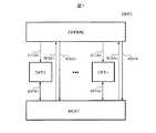
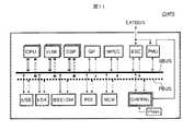
図1は、本発明の電力制御方式を用いたチップCHP1の概念的実施例を示す図である。CKT1〜CKTnはサブ回路、MCKTはメイン回路、CHPKNLはチップ統括電力制御部(以下、チップカーネルと呼ぶ)である。DATS1〜DATSnはデータ信号(データ線)、CTLS1〜CTLSnは電力制御信号(電力制御線)、REQS1〜REQSnはリクエスト信号(リクエスト線)、ACKS1〜ACKSnはアクノレッジ信号(アクノレッジ線)である(なお、信号と当該信号を伝達するための配線とは同じ符号であらわすものとする)。メイン回路MCKTは、サブ回路CKT1〜CKTnを以下に示す方式に従って使用し、データ線DATS1〜DATSnを介してデータの授受を行うことで、チップCHP1に要求される機能を実現している。ここで、メイン回路MCKTは、電力制御されない回路であって、各サブ回路CKT1〜CKTnの使用権をもつ回路である。チップCHIP1に電源投入されるとともにメイン回路MCKTはアクティブ状態となり、以下のようにサブ回路CKT1〜CKTnを起動する。メイン回路MCKTがサブ回路CKT1を使用する場合を例に、起動の手順を説明する。<First Embodiment>
FIG. 1 is a diagram showing a conceptual embodiment of a chip CHP1 using the power control method of the present invention. CKT1 to CKTn are sub-circuits, MCKT is a main circuit, and CHPKNL is a chip integrated power control unit (hereinafter referred to as a chip kernel). DATS1 to DATSn are data signals (data lines), CTLS1 to CTLSn are power control signals (power control lines), REQS1 to REQSn are request signals (request lines), and ACKS1 to ACKSn are acknowledge signals (acknowledge lines). The signal and the wiring for transmitting the signal are represented by the same symbol). The main circuit MCKT uses the sub-circuits CKT1 to CKTn according to the following method, and exchanges data via the data lines DATS1 to DATSn, thereby realizing a function required for the chip CHP1. Here, the main circuit MCKT is a circuit that is not subjected to power control and has a right to use each of the sub-circuits CKT1 to CKTn. As the chip CHIP1 is powered on, the main circuit MCKT becomes active and activates the sub-circuits CKT1 to CKTn as follows. The startup procedure will be described by taking as an example the case where the main circuit MCKT uses the sub circuit CKT1.
チップCHIP1に電源投入された段階では、メイン回路MCKTはアクティブ状態であり、サブ回路CKT1〜CKTnは消費電力が低減されるよう制御された待機状態にある。待機状態としては、さまざまな態様がありうる(図2に関して後述するSTB状態、SLP状態はここでいう待機状態に含まれる)。消費電力を低減するためには、(1)サブ回路CKT1〜CKTnにクロックを供給しない、(2)電源電圧を供給しない、(3)リーク電流を抑制する等の方法がある。チップの消費電力が許容範囲内に収まる限り、これらの方法を特性に応じて組み合わせて用いればよい。 At the stage when power is supplied to the chip CHIP1, the main circuit MCKT is in an active state, and the sub-circuits CKT1 to CKTn are in a standby state controlled so as to reduce power consumption. There can be various modes as the standby state (STB state and SLP state described later with reference to FIG. 2 are included in the standby state here). In order to reduce power consumption, there are methods such as (1) not supplying a clock to the sub-circuits CKT1 to CKTn, (2) not supplying a power supply voltage, and (3) suppressing a leakage current. As long as the power consumption of the chip is within an allowable range, these methods may be used in combination according to the characteristics.
例えば、電源電圧を供給し、クロックの供給のみを停止するように制御すると、クロック供給のみを再開することで回路動作を再開できるので、回路動作を迅速に再開できる。一方、(2)、(3)の方法を併用する場合には、(1)の方法のみを用いる場合よりもスタティックな消費電力も削減でき、より低消費電力化が可能である。待機状態については、回路ごとに、クロックの供給のみを停止する、クロック及び電源電圧の供給を停止するといったように、その制御方法を異ならせることも可能である。 For example, when the power supply voltage is supplied and control is performed so that only the clock supply is stopped, the circuit operation can be restarted by restarting only the clock supply, so that the circuit operation can be restarted quickly. On the other hand, when the methods (2) and (3) are used in combination, static power consumption can be reduced as compared with the case where only the method (1) is used, and lower power consumption is possible. In the standby state, the control method may be different for each circuit, such as stopping only the supply of the clock or stopping the supply of the clock and the power supply voltage.
メイン回路MCKTがサブ回路CKT1を使用する場合、メイン回路MCKTはチップカーネルCHPKNLにリクエスト信号REQS1により、サブ回路CKT1の使用要求を申請する。使用許可はチップカーネルCHPKNLによってアクノレッジ信号ACKS1によりメイン回路MCKTに通知され、またサブ回路CKT1は電力制御信号CTLS1により待機状態から通常動作可能な状態に移行する。メイン回路MCKTはサブ回路CKT1を使用し、このときのデータの授受はデータ線DATS1を介して行われる。アクノレッジ線ACKS1によって使用許可が得られている場合に限り、メイン回路MCKTはサブ回路CKT1を使用することができ、使用許可が得られない限り、メイン回路MCKTはサブ回路CKT1を使用することはできない。 When the main circuit MCKT uses the sub circuit CKT1, the main circuit MCKT applies a request for use of the sub circuit CKT1 to the chip kernel CHPKNL by using the request signal REQS1. The use permission is notified to the main circuit MCKT by the acknowledge signal ACKS1 by the chip kernel CHPKNL, and the sub circuit CKT1 shifts from the standby state to a state in which it can normally operate by the power control signal CTLS1. The main circuit MCKT uses the sub circuit CKT1, and data exchange at this time is performed via the data line DATS1. The main circuit MCKT can use the sub circuit CKT1 only when the use permission is obtained by the acknowledge line ACKS1, and the main circuit MCKT cannot use the sub circuit CKT1 unless the use permission is obtained. .
チップカーネルCHPKNLは、サブ回路の使用を開始した場合に予め設定されたチップ許容電力Pmaxを超えるようであればその使用を許可できない。そこで、チップカーネルCHPKNLはサブ回路使用要求に対して、電力制御線CTLS1〜CTLSnを用いて、チップの消費電力が予め設定されたチップ許容電力Pmax以下になるように各サブ回路の動作状態を制御しながら、使用要求されたサブ回路が使用できる状態にする。その後、サブ回路CKT1〜CKTnの使用許可を、アクノレッジ信号ACKS1〜ACKSnによりメイン回路MCKTに与える。 If the chip kernel CHPKNL exceeds the preset chip allowable power Pmax when the use of the sub-circuit is started, the chip kernel CHPKNL cannot permit the use. Therefore, the chip kernel CHPKNL uses the power control lines CTLS1 to CTLSn in response to subcircuit usage requests, and controls the operating state of each subcircuit so that the power consumption of the chip is less than the preset chip allowable power Pmax. On the other hand, the subcircuit requested to be used is made available. Thereafter, the use permission of the sub-circuits CKT1 to CKTn is given to the main circuit MCKT by the acknowledge signals ACKS1 to ACKSn.
なお、使用要求が許可できない場合には、アクノレッジ信号ACKSをメイン回路MCKTに与えない等により不許可をメイン回路に通知することで、メイン回路MCKTはそのサブ回路の使用を遅らせるか、別のサブ回路の使用を中止してそのサブ回路を優先使用するか判断することができる。また、チップカーネルCHPKNLは待機状態にあるサブ回路のリーク電流を低減することにより、消費電力のマージンを上げることができる。 If the use request cannot be permitted, the main circuit MCKT delays the use of the sub circuit by notifying the main circuit of the non-permission, for example, by not providing the acknowledge signal ACKS to the main circuit MCKT, or another sub circuit. It is possible to determine whether to stop using the circuit and preferentially use the subcircuit. Further, the chip kernel CHPKNL can increase the margin of power consumption by reducing the leakage current of the sub circuit in the standby state.
以下、電力制御信号CTLS1〜CTLSnを用いたサブ回路CKT1〜CKTnの電力制御方法(消費電力の異なる複数の動作状態(待機状態を含む)を作る方法をいう)の実施例を示す。さらに、チップの消費電力が、予め設定されたチップ許容電力Pmax以下になるように各サブ回路の動作状態を制御して使用要求されたサブ回路が使用できる状態にする動作状態制御方法(以下、サブ回路スケジューリングと呼ぶ)の実施例を示す。 Hereinafter, an embodiment of a power control method (referring to a method for creating a plurality of operation states (including a standby state) with different power consumption) of the sub-circuits CKT1 to CKTn using the power control signals CTLS1 to CTLSn will be described. Further, an operation state control method (hereinafter, referred to as “a state where a sub circuit requested for use” can be used by controlling the operation state of each sub circuit so that the power consumption of the chip is equal to or less than a preset chip allowable power Pmax. (Referred to as subcircuit scheduling).
図2はサブ回路CKT1〜CKTnの電力制御方法の実施例を示している。G1〜G3はANDゲート、MP1はPMOSトランジスタ、MN1はNMOSトランジスタ、MN2はMN1のゲート酸化膜厚tox1よりも厚いゲート酸化膜tox2を持ち、MN1のしきい値電圧(絶対値)Vth1よりも高いしきい値電圧(絶対値)Vth2であるNMOSトランジスタ、VDDとVSSはそれぞれ正側と負(グランド)側の電源線である。なお、ゲート絶縁膜の厚さは物理的な長さのみならず電気的な長さによって決定される。すなわち、MN1とMN2とを同じ絶縁膜材料で構成してその物理的な絶縁膜厚を異ならせることにより、またはMN1とMN2とで物理的な絶縁膜厚は等しいけれどもそれぞれ誘電率の異なる絶縁膜材料を用いることにより、またはMN1とMN2とで絶縁膜材料、物理的な厚さともに異ならせることにより実現することができる。 FIG. 2 shows an embodiment of a power control method for the sub-circuits CKT1 to CKTn. G1 to G3 are AND gates, MP1 is a PMOS transistor, MN1 is an NMOS transistor, MN2 has a gate oxide film tox2 that is thicker than the gate oxide film thickness tox1 of MN1, and is higher than the threshold voltage (absolute value) Vth1 of MN1 NMOS transistors VDD and VSS having a threshold voltage (absolute value) Vth2 are power lines on the positive side and the negative (ground) side, respectively. Note that the thickness of the gate insulating film is determined not only by the physical length but also by the electrical length. In other words, MN1 and MN2 are made of the same insulating film material and have different physical insulating film thickness, or MN1 and MN2 have the same physical insulating film thickness but have different dielectric constants. This can be realized by using a material or by making the insulating film material and physical thickness different between MN1 and MN2.
LGはサブ回路の機能を実現するための回路であり、ここではフリップフロップFFと、PMOSトランジスタMP1とNMOSトランジスタMN1からなるインバータを例示している。また、回路LGと負側電源線の間にNMOSトランジスタMN2が接続されており、NMOSトランジスタMN2のドレインに接続された配線は仮想接地線VVSSとして回路LGの負側電源線として使用されている。 LG is a circuit for realizing the function of the sub-circuit, and here, a flip-flop FF, and an inverter composed of a PMOS transistor MP1 and an NMOS transistor MN1 are illustrated. Further, the NMOS transistor MN2 is connected between the circuit LG and the negative power supply line, and the wiring connected to the drain of the NMOS transistor MN2 is used as the virtual power supply line VVSS as the negative power supply line of the circuit LG.
電力制御信号(電力制御線)CTLSはCTLSa〜CTLScによって構成されている。第1の電力制御信号CTLSaが'H'の場合には、NMOSトランジスタMN2はオン状態となり、回路LGに電源が供給される。また、第1の電力制御信号CTLSaが'L'の場合には、NMOSトランジスタMN2はオフ状態となり、回路LGへの給電が停止される。また、第2の電力制御信号CTLSbが'H'の場合には、ANDゲートG1を介してクロック信号CLKがGCLKに伝播され、回路LG内にクロックが分配される。また、第2の電力制御信号CTLSbが'L'の場合には、ANDゲートG1の出力GCLKは'L'となるため、LG内のクロック分配は停止される。 The power control signal (power control line) CTLS is composed of CTLSa to CTLSc. When the first power control signal CTLSa is “H”, the NMOS transistor MN2 is turned on, and power is supplied to the circuit LG. On the other hand, when the first power control signal CTLSa is “L”, the NMOS transistor MN2 is turned off and the power supply to the circuit LG is stopped. When the second power control signal CTLSb is “H”, the clock signal CLK is propagated to GCLK via the AND gate G1, and the clock is distributed in the circuit LG. When the second power control signal CTLSb is “L”, the output GCLK of the AND gate G1 is “L”, and the clock distribution in the LG is stopped.
以下、(CTLSa,CTLSb) = (H',H')の時をACT状態、(CTLSa,CTLSb) = (H',L')の時をSTB状態、(CTLSa,CTLSb) = (L',L')の時をSLP状態と呼ぶ。 Hereinafter, when (CTLSa, CTLSb) = (H ', H'), ACT state, when (CTLSa, CTLSb) = (H ', L'), STB state, (CTLSa, CTLSb) = (L ', The time of L ′) is called the SLP state.
ACT状態では、回路LGは給電されているためサブスレッショルドリーク電流やゲートリーク電流等による電力が消費され、さらに、クロックも配分されるために負荷の充放電による電力も消費する。一方、STB状態では、回路LGは給電されているためサブスレッショルドリーク電流やゲートリーク電流等による電力が消費されるが、クロックが配分されないために負荷の充放電による電力は消費されない。また、SLP状態では、回路LGに給電されないためサブスレッショルドリーク電流やゲートリーク電流等による電力は消費されない。また、MN2のしきい値電圧vth2は高く、かつ厚い酸化膜tox2をもつため、NMOSトランジスタMN2のオフ時に大きなゲートリーク電流が流れることがなく、NMOSトランジスタMN2を介して回路LGのサブスレッショルドリーク電流が流れることもない。また当然、クロックも配分されないために負荷の充放電による電力も消費されない。 In the ACT state, the circuit LG is supplied with power, so that power due to the subthreshold leakage current, gate leakage current, etc. is consumed. Further, since the clock is also distributed, power due to charging / discharging of the load is also consumed. On the other hand, in the STB state, the circuit LG is supplied with power, so that power due to the subthreshold leakage current, gate leakage current, and the like is consumed. However, since the clock is not distributed, power due to load charging / discharging is not consumed. In the SLP state, power is not consumed by the sub-threshold leakage current, gate leakage current, or the like because power is not supplied to the circuit LG. Further, since the threshold voltage vth2 of MN2 is high and the oxide film tox2 is thick, a large gate leakage current does not flow when the NMOS transistor MN2 is turned off, and the subthreshold leakage current of the circuit LG is passed through the NMOS transistor MN2. Does not flow. Of course, since no clock is allocated, power due to charging / discharging of the load is not consumed.
第3の電力制御信号CTLScは、LGの入力信号INと出力信号OUTに接続されたANDゲートG2およびG3に接続されている。CTLScが'H'の場合、サブ回路CKTの外部から入力された信号INは、ANDゲートG2を介してそのまま信号GINとして回路LGに伝播され、回路LGからの出力OUTもANDゲートG3を介してそのまま出力GOUTとしてサブ回路CKTの外部に出力される。一方、第3の電力制御信号CTLScが'L'の場合、ANDゲートG2及びG3の出力は'L'となり、サブ回路CKTの外部から入力された信号INは回路LGに伝播されず、回路LGからの出力OUTがいかなる電圧であっても、サブ回路CKTの出力GOUTは'L'のままになる。 The third power control signal CTLSc is connected to AND gates G2 and G3 connected to the LG input signal IN and output signal OUT. When CTLSc is 'H', the signal IN input from the outside of the subcircuit CKT is directly propagated to the circuit LG as the signal GIN through the AND gate G2, and the output OUT from the circuit LG is also transmitted through the AND gate G3. The output is output as it is to the outside of the sub circuit CKT. On the other hand, when the third power control signal CTLSc is “L”, the outputs of the AND gates G2 and G3 are “L”, and the signal IN input from the outside of the sub circuit CKT is not propagated to the circuit LG, and the circuit LG The output GOUT of the sub-circuit CKT remains “L” regardless of the voltage of the output OUT from.
上記のようなANDゲートG2による入力信号の伝播抑制によって、不必要な信号GINの遷移を防止できる。例えば回路LGにクロックが分配されないSTB状態やSLP状態のような回路LGを使用しないときに第3の電力制御信号CTLScを'L'にすることで、不必要な遷移による電力消費を小さくできる。また、ANDゲートG3による出力信号の固定は、例えば回路LGに給電されないSLP状態のときに信号GOUTの電圧が'H'や'L'以外の不定電圧になることを回避でき、信号GOUTを入力とする回路LGの次段回路の貫通電流等を防止できる。したがって、特に限定しないが、STB状態とSLP状態で第3の電力制御信号CTLScが'L'になるようにすれば効果的であり、その場合、第3の電力制御信号CTLScと第2の電力制御信号CTLSbとは共通化すればよい。 By suppressing the propagation of the input signal by the AND gate G2 as described above, unnecessary transition of the signal GIN can be prevented. For example, the power consumption due to unnecessary transition can be reduced by setting the third power control signal CTLSc to “L” when the circuit LG such as STB state or SLP state where the clock is not distributed to the circuit LG is not used. Also, fixing the output signal by the AND gate G3 can prevent the voltage of the signal GOUT from becoming an indeterminate voltage other than 'H' or 'L' in the SLP state where power is not supplied to the circuit LG, for example, and input the signal GOUT The through current of the next stage circuit of the circuit LG can be prevented. Accordingly, although not particularly limited, it is effective if the third power control signal CTLSc is set to “L” in the STB state and the SLP state. In this case, the third power control signal CTLSc and the second power are effective. The control signal CTLSb may be shared.
なお、図2のように電源スイッチとして高しきい値・厚酸化膜のNMOSトランジスタMN2を用いた場合、文献5のようにPMOSトランジスタを電源スイッチに用いた場合と比較して以下の効果がある。
(1)電源スイッチがオン時には、電源インピーダンスを下げるためにオン抵抗を小さくする必要がある。NMOSトランジスタは、PMOSトランジスタよりも同じゲート幅で小さなオン抵抗が得られる。
(2)VDDが低電圧化した場合でも、NMOSトランジスタMN2のオン状態時に、NMOSトランジスタMN2のゲート電圧にVDDよりも高い電圧(VDDH)が印加できる。これにより、NMOSトランジスタのオン抵抗を小さくできる。特に、NMOSトランジスタMN2を、チップの外部とのインターフェース回路(I/O回路)で用いる厚酸化膜MOSトランジスタと同じ高耐圧MOSトランジスタで構成すれば、製造プロセスの複雑化を防ぐことができる。またその場合、VDDHをI/O電圧(VDDQ)と同じ電圧にすることができ、VDDHのための電圧発生回路を設ける必要がなくなる。もちろん、「同じトランジスタ」という場合に製造ばらつきによる違いは許容される。In addition, when the NMOS transistor MN2 having a high threshold voltage and a thick oxide film is used as the power switch as shown in FIG. 2, the following effects are obtained as compared with the case where the PMOS transistor is used as the power switch as in
(1) When the power switch is on, it is necessary to reduce the on-resistance in order to lower the power impedance. The NMOS transistor has a smaller on-resistance with the same gate width than the PMOS transistor.
(2) Even when VDD is lowered, a voltage (VDDH) higher than VDD can be applied to the gate voltage of the NMOS transistor MN2 when the NMOS transistor MN2 is on. Thereby, the on-resistance of the NMOS transistor can be reduced. In particular, if the NMOS transistor MN2 is composed of the same high voltage MOS transistor as the thick oxide film MOS transistor used in the interface circuit (I / O circuit) with the outside of the chip, the manufacturing process can be prevented from becoming complicated. In this case, VDDH can be set to the same voltage as the I / O voltage (VDDQ), and there is no need to provide a voltage generation circuit for VDDH. Of course, in the case of “same transistors”, differences due to manufacturing variations are allowed.
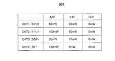
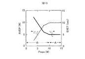
図3は、図2で示した電力制御方法を用いた場合の、サブ回路の消費電力の例を示している。ここでは、サブ回路として、マイクロプロセッサCPUと、浮動小数点演算回路FPU、シグナルプロセッサDSP、通信回路RFを例として用いた。それぞれの回路規模や回路の特性によって、ACT状態、STB状態、SLP状態の三状態によって例えば図3で示されたように消費電力が変化する。もちろん、ACT状態時の電力が最も大きく、その次にSTB状態の電力が大きく、SLP状態では電源が遮断されるためにほとんど電力を消費しない。 FIG. 3 shows an example of power consumption of the sub-circuit when the power control method shown in FIG. 2 is used. Here, a microprocessor CPU, a floating point arithmetic circuit FPU, a signal processor DSP, and a communication circuit RF are used as examples of sub-circuits. Depending on the circuit scale and circuit characteristics, the power consumption varies as shown in FIG. 3, for example, depending on the three states of the ACT state, STB state, and SLP state. Of course, the power in the ACT state is the largest, the power in the STB state is the next largest, and the power is cut off in the SLP state, so little power is consumed.
図4はACT状態、STB状態、SLP状態の三状態を含むサブ回路CKTの状態遷移図の実施例を示している。SLP状態からSTB状態に遷移する間とSTB状態からACT状態に遷移する間に、それぞれS1とS2で示された中間状態が存在する。これらの中間状態を設けることで各状態の遷移を安定して行うことができる。 FIG. 4 shows an example of a state transition diagram of the sub-circuit CKT including three states of ACT state, STB state, and SLP state. Between the transition from the SLP state to the STB state and between the transition from the STB state to the ACT state, there are intermediate states indicated by S1 and S2, respectively. By providing these intermediate states, the transition of each state can be performed stably.
例えば、SLP状態からSTB状態への遷移では回路LGへの電源供給が行われる。回路LGの回路規模にも依存するが、一般に回路LGに電源を投入した時には大きな突入電流が流れる。この突入電流は回路LG内の負荷の充電による電流と、充電過程での貫通電流等から成っている(一般にCMOS回路は、入力ノード電圧が正側か負(グランド)側の電源電圧電位以外の電位である場合、大きな貫通電流が流れる)。この突入電流を特性するためには、電源の投入をゆっくりと実行する方法が効果的である。具体的にはMOSトランジスタMN2のゲート信号を小さいスルーレートで'L'から'H'に遷移させる。これによって突入電流を小さく抑えることができ、電源バンプ等を小さくでき、結果的にチップ全体の誤差動をも防ぐことができる。この遷移過程を状態S1として処理する。完全に回路LGへの電力給電が完了したことを検出してから(T2)、STB状態に遷移することで、電源が非安定であることによる誤作動を防ぐことができる。 For example, in the transition from the SLP state to the STB state, power is supplied to the circuit LG. Although depending on the circuit scale of the circuit LG, generally a large inrush current flows when the circuit LG is turned on. This inrush current consists of the current due to the charging of the load in the circuit LG and the through current during the charging process. (In general, the CMOS circuit has a voltage other than the power supply voltage potential on the positive side or negative (ground) side of the input node voltage. When it is at a potential, a large through current flows). In order to characterize this inrush current, a method of slowly turning on the power is effective. Specifically, the gate signal of the MOS transistor MN2 is changed from “L” to “H” at a small slew rate. As a result, the inrush current can be reduced, the power supply bumps and the like can be reduced, and as a result, the error movement of the entire chip can be prevented. This transition process is processed as state S1. After detecting that the power supply to the circuit LG is completely completed (T2), the transition to the STB state can prevent malfunction due to the power supply being unstable.
なお、NMOSトランジスタMN2のゲート信号を小さいスルーレートで'L'から'H'に遷移させた場合、MN2のゲート信号電位をモニタすることで、回路LGの電源供給の完了を検出できる。すなわち、回路LG内のノードの充放電時間よりも遅い時間でMOSトランジスタMN2のゲート信号を遷移させればよい。MOSトランジスタMN2のゲート信号が完全に'H'になった頃には、回路LG内のノードの充電も完了していることになるからである。遅い時間でMOSトランジスタMN2のゲート信号を遷移させるためには、例えば比較的大きな出力インピーダンスのドライバでMOSトランジスタMN2のゲートを駆動すればよい。なお、この方式ではMOSトランジスタMN2のゲートインピーダンスが高くなる。クロストーク等のノイズがこの高インピーダンス配線に悪影響を及ぼす懸念がある場合、MN2のゲート信号電位をモニタしてLGの電源供給の完了を検出した後に、比較的小さな出力インピーダンスのドライバでMOSトランジスタMN2のゲートを駆動し直せばよい。後述する図9の構成例にこのための構成を示す。バッファBUF中のドライバC1、C2、C3が上記のようなMOSトランジスタMN2の駆動方法を実現する回路になっている。ドライバC2が上記比較的大きな出力インピーダンスのドライバであって、まず最初にドライバC2でMOSトランジスタMN2を駆動する。ドライバC1が上記比較的小さな出力インピーダンスのドライバで、ドライバC3はMN2のゲート信号電位をモニタする回路である。 When the gate signal of the NMOS transistor MN2 is changed from “L” to “H” at a low slew rate, the completion of power supply to the circuit LG can be detected by monitoring the gate signal potential of the MN2. That is, the gate signal of the MOS transistor MN2 may be shifted in a time later than the charge / discharge time of the node in the circuit LG. This is because when the gate signal of the MOS transistor MN2 becomes completely “H”, charging of the node in the circuit LG is also completed. In order to transition the gate signal of the MOS transistor MN2 in a later time, the gate of the MOS transistor MN2 may be driven by a driver having a relatively large output impedance, for example. In this method, the gate impedance of the MOS transistor MN2 is increased. If there is a concern that noise such as crosstalk may adversely affect this high impedance wiring, after monitoring the gate signal potential of MN2 and detecting the completion of LG power supply, the MOS transistor MN2 with a relatively low output impedance driver It is sufficient to drive the gate again. A configuration for this is shown in a configuration example of FIG. 9 described later. The drivers C1, C2, and C3 in the buffer BUF are a circuit that realizes the driving method of the MOS transistor MN2 as described above. The driver C2 is a driver having the above relatively large output impedance. First, the driver C2 drives the MOS transistor MN2. The driver C1 is a driver having a relatively small output impedance, and the driver C3 is a circuit that monitors the gate signal potential of MN2.
また、上記S1の効果は、STB状態からACT状態の遷移でも同様のことがいえる。例えば、クロック信号の分配に所定時間を要する場合、STB状態からACT状態への遷移に中間状態S2を設けることにより、それに要する時間を吸収する。 Moreover, the same effect can be said for the effect of S1 in the transition from the STB state to the ACT state. For example, when a predetermined time is required for the distribution of the clock signal, the intermediate time S2 is provided in the transition from the STB state to the ACT state, thereby absorbing the time required for the time.
なお、図2には図示していないが、デカップリングコンデンサをVDDとVSSの間に接続する方が望ましい。また、デカップリングコンデンサをVDDとVVSSの間に接続すれば、VDDとVSSの間に接続した場合よりもノイズ除去性能は高くなる。ただし、NMOSトランジスタMN2のオン・オフにともなってデカップリングコンデンサに蓄えられている電荷も充放電されることになり、不要な電力を消費することになる。 Although not shown in FIG. 2, it is desirable to connect a decoupling capacitor between VDD and VSS. Also, if a decoupling capacitor is connected between VDD and VVSS, the noise removal performance will be higher than when it is connected between VDD and VSS. However, as the NMOS transistor MN2 is turned on / off, the charge stored in the decoupling capacitor is also charged / discharged, and unnecessary power is consumed.
また、図2で示したMOSトランジスタの基板端子の接続先は、特に図2の接続方法に限定しない。さらに、図2ではNMOSトランジスタMN2を用いた電源スイッチの方法を用いてサブスレッショルドリーク電流を制御しているが、文献4で記述されているような基板バイアス制御の方法を用いてもよい。 Further, the connection destination of the substrate terminal of the MOS transistor shown in FIG. 2 is not particularly limited to the connection method of FIG. Further, in FIG. 2, the subthreshold leakage current is controlled using the power switch method using the NMOS transistor MN2, but the substrate bias control method described in
また、図3では各サブ回路LGをマイクロプロセッサCPUやシグナルプロセッサDSP等の大きな回路ブロックを仮定したが、特に各サブ回路の回路規模は限定しない。例えば一つの演算器をサブ回路として扱ったり、一つのメモリ回路をサブ回路として扱ってもよい。多くの小規模回路に分割した方が、きめ細かい電力制御ができる。 In FIG. 3, each subcircuit LG is assumed to be a large circuit block such as a microprocessor CPU or a signal processor DSP, but the circuit scale of each subcircuit is not particularly limited. For example, one arithmetic unit may be handled as a sub circuit, or one memory circuit may be handled as a sub circuit. Finer power control can be achieved by dividing the circuit into many smaller circuits.
また、図3では三種類の状態を仮定したが、SLP状態とACT状態の二種類や、STB状態とACT状態の二種類でもよい。さらに4つ以上の状態数を設けてもよい。また、これらの状態数は各サブ回路ごとに設定でき、例えば回路によっては2状態をもつもの、2状態持つものが混在していてもよい。状態数を多く設けた方が、きめ細かい電力制御ができる。 Further, although three types of states are assumed in FIG. 3, two types of SLP state and ACT state, or two types of STB state and ACT state may be used. Further, four or more states may be provided. The number of states can be set for each sub-circuit. For example, some circuits may have two states and two states may exist together. Finer power control can be achieved by providing a larger number of states.
また、状態遷移の方法は図4で示したものには限定されない。チップあるいはサブ回路ごとに最適な状態遷移方法を用いることができる。 Further, the state transition method is not limited to that shown in FIG. An optimum state transition method can be used for each chip or subcircuit.
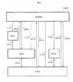
図5にサブ回路スケジューリングの実施例を示す。ここでは説明を簡単にするために、チップ許容電力Pmaxを250mWとして、サブ回路CKT〜CKTnまでの回路のトータル電力消費が200mW以下になるように、各サブ回路CKT1〜CKTnの状態を図4の状態遷移に従って遷移させた例を示した。例えば、時刻0ではCKT1はACT状態で、CKT2とCKT4はSTB状態で、CKT3はSLP状態であり、100mWの電力を消費している。ここで、時刻1ではCKT2がACT状態に遷移しており、150mWの電力消費に増加している。サブ回路の電力消費の合計がPmax以下でなるべく小さくなるように各サブ回路の状態を制御している。 FIG. 5 shows an example of subcircuit scheduling. Here, for simplicity of explanation, the state of each of the subcircuits CKT1 to CKTn is set so that the chip allowable power Pmax is 250 mW and the total power consumption of the circuits from the subcircuits CKT to CKTn is 200 mW or less. An example of transition according to state transition is shown. For example, at
サブ回路スケジューリングの具体的な手法としては、例えばMaurice J. Bach著(坂本文 他訳)、 「UNIXカーネルの設計」コンピュータサイエンス誌BIT別冊、共立出版、1990年10月発行(以下、文献6と記す)の211頁から記載されているようなUNIX(登録商標、以下同様)オペレーティングシステムのプロセススケジューリングや、同じく文献6文献の231頁から記載されているようなUNIXオペレーティングシステムのメモリ管理と同様の考え方を用いることができる。すなわち、UNIXオペレーティングシステムではメモリ容量に上限があるというメモリ制約と、CPUの数が限られているために同時に実行できるプロセスの数が制約されるという実行制約から、複数のプロセスのスワップインとスワップアウト等を行って、全てのプロセスが定められたスケジューリング規則に従って実行している。一方、本発明のチップでは、消費電力に上限があるという制約から複数のサブ回路の電力制御を行い、全てのサブ回路が定められたスケジューリング規則に従って実行する。 Specific methods for subcircuit scheduling include, for example, Maurice J. Bach (Sakamoto et al.), “UNIX Kernel Design”, BIT volume, Computer Science magazine, published in October 1990 (hereinafter referred to as Reference 6). The same as the UNIX operating system process scheduling as described from page 211 of the above) and the UNIX operating system memory management as described from page 231 of the
UNIXオペレーティングシステムにおけるプロセススケジューリングやメモリ管理には多くの手法が存在するが、それぞれのスケジューリング手法を本発明のサブ回路スケジューリングに適用することができる。ここでは特にその方法は限定しない。例えば、UNIXオペレーティングシステムでプロセスがメモリ上に存在(スワップイン状態)して実行中の状態が本発明のACT状態、UNIXオペレーティングシステムでプロセスがメモリ上に存在(スワップイン状態)して実行待ちの状態が本発明のSTB状態、UNIXオペレーティングシステムでプロセスがメモリ上に存在しない状態(スワップアウト状態)が本発明のSLP状態に対応させることができる。 There are many methods for process scheduling and memory management in the UNIX operating system, and each scheduling method can be applied to the sub-circuit scheduling of the present invention. Here, the method is not particularly limited. For example, in a UNIX operating system, a process exists in memory (swap-in state) and is being executed, and in the ACT state of the present invention, in a UNIX operating system, a process exists in memory (swap-in state) and is waiting for execution The state can correspond to the STB state of the present invention, and the state where the process does not exist in the memory (swap-out state) in the UNIX operating system can correspond to the SLP state of the present invention.
以上で述べたUNIXオペレーティングシステム以外でも、米国マイクロソフト社のウィンドウズ(登録商標)のようなオペレーティングシステムが多く存在するが、それらの方法で使用されているプロセススケジューリング方式やメモリ管理方式も同様に利用できる。μITRONのようなリアルタイムオペレーティングシステムと呼ばれるものも多く存在し、それらのオペレーティングシステムはリアルタイム性を保証するために特別のスケジューリングを行っている。これらも本発明のサブ回路スケジューリングに適用できる。 In addition to the UNIX operating systems described above, there are many operating systems such as Microsoft Windows (registered trademark), but the process scheduling method and memory management method used in these methods can be used as well. . There are many so-called real-time operating systems such as μITRON, and these operating systems perform special scheduling to guarantee real-time performance. These can also be applied to the sub-circuit scheduling of the present invention.
なお、図5では説明の簡単化のため、サブ回路CKT〜CKTnまでの回路のトータル電力消費が200mW以下になるようなサブ回路スケジューリングの実施例を示した(なお、後で記す図7の実施例の説明でも同様に、電力状態遷移に伴う電力消費は無視している)。しかし、本発明のサブ回路スケジューリングは、チップの消費電力が予め設定されたチップ許容電力Pmax以下になるように、各サブ回路の動作状態を制御しながら、使用要求されたサブ回路が使用できる状態にする必要がある。そのためには各サブ回路の状態遷移にともなう電力消費も考慮する必要がある。特に、電源のオン・オフを伴う遷移では、遷移自体による電力消費が無視できない大きさになることが多い。これは電源の遮断時には、回路内の多くのノードの電荷を放電することになり、電源の投入は前記ノードの電荷を充電することになるからである。 For the sake of simplicity, FIG. 5 shows an example of sub-circuit scheduling in which the total power consumption of the circuits from sub-circuits CKT to CKTn is 200 mW or less (the implementation of FIG. 7 described later). In the description of the example, the power consumption accompanying the power state transition is also ignored). However, the sub circuit scheduling according to the present invention is a state in which the sub circuit requested to be used can be used while controlling the operation state of each sub circuit so that the power consumption of the chip is less than or equal to the preset chip allowable power Pmax. It is necessary to. For that purpose, it is necessary to consider the power consumption accompanying the state transition of each sub-circuit. In particular, in a transition involving turning on / off of a power source, power consumption due to the transition itself often becomes a magnitude that cannot be ignored. This is because when the power is shut off, the charges of many nodes in the circuit are discharged, and when the power is turned on, the charges of the nodes are charged.
このような多数の遷移による電力増加のオーバヘッドを抑制するためには、遷移頻度を抑制する方法が効果的である。例えば、ある一定時間サブ回路が使用されなかったときだけ、電源がオフされる状態に遷移するようにする。そこで、各サブ回路の動作状態遷移頻度を制約する回路をチップカーネルCHPKNLに設けるか、各サブ回路CKTに動作状態遷移頻度を制約する回路を設ければよい。そのためには、各サブ回路CKTあるいはチップカーネルCHPKNLに、各サブ回路における各動作状態遷移で消費する電力情報を管理格納しておく。例えば、ACT状態からSLP状態またはSTB状態からSLP状態に遷移する場合に、電源を供給したまま消費電力が漸減する(あるいは一定に維持される)ような中間状態を設けておく(このような中間状態の設定が上述の電力情報に相当する)。この中間状態の数は電源のオン・オフを伴う遷移による電力消費が大きい場合には多く、小さい場合には少なく設定しておくことが望ましい。一つの制御の方法を例示すると、サブ回路の使用が終了してACT状態からSTB状態に遷移するにあたり、5つの中間状態(S1〜5)を順次経由してSTB状態に至るように設定し、かつ中間状態S5からSTB状態に遷移するときに電源をオフするようにする。これら中間状態の遷移は一定周期で行うようにする。この場合、遷移頻度が大きい場合には、STB状態に遷移してしまう前、すなわち中間状態(例えばS3)からACT状態に遷移することになり、電源のオン・オフを伴う電力消費の発生を防止できる。もちろん、動作状態遷移にともなう電力消費が無視できる場合には、動作状態遷移頻度を制約する回路を省略してもよい。 In order to suppress the overhead of power increase due to such a large number of transitions, a method of suppressing the transition frequency is effective. For example, only when the sub-circuit is not used for a certain period of time, the power supply is turned off. Therefore, a circuit that restricts the operation state transition frequency of each subcircuit may be provided in the chip kernel CHPKNL, or a circuit that restricts the operation state transition frequency may be provided in each subcircuit CKT. For this purpose, power information consumed in each operation state transition in each sub circuit is managed and stored in each sub circuit CKT or chip kernel CHPKNL. For example, when transitioning from the ACT state to the SLP state or from the STB state to the SLP state, an intermediate state is provided in which the power consumption gradually decreases (or is maintained constant) while the power is supplied (such intermediate state). The state setting corresponds to the power information described above). It is desirable to set the number of intermediate states to be large when the power consumption due to the transition accompanied by power on / off is large, and to be small when the power consumption is small. As an example of one control method, when the use of the sub-circuit is finished and the transition from the ACT state to the STB state is performed, the intermediate state (S1 to 5) is sequentially set to reach the STB state. In addition, the power is turned off when the intermediate state S5 transits to the STB state. The transition of these intermediate states is performed at a constant cycle. In this case, if the transition frequency is high, the transition to the STB state is made, that is, the transition from the intermediate state (for example, S3) to the ACT state, thereby preventing the occurrence of power consumption accompanying power on / off. it can. Of course, when the power consumption accompanying the operation state transition is negligible, the circuit that restricts the operation state transition frequency may be omitted.
このようにして、各サブ回路CKTの状態遷移時の電力消費を含めて、チップの消費電力がある決められた値以下になるように制御する。また、サブ回路スケジューリングは、チップの消費電力をPmax以下にするようにスケジューリングするだけではなく、チップの処理性能が高くなるように考慮されながら、チップの消費電力をPmax以下のなるべく小さな値になるように制御することが望ましい。 In this way, the power consumption of the chip is controlled to be less than a predetermined value including the power consumption at the time of state transition of each sub-circuit CKT. In addition, the sub-circuit scheduling not only schedules the chip power consumption to be Pmax or less, but also considers the chip processing performance to be high, while reducing the chip power consumption to a value as small as Pmax or less. It is desirable to control as follows.
電力制約の仕方は以上に限られない。チップ内に10個のサブ回路CKT1〜CKT10が存在する場合、その中のn個(1≦n≦10)のサブ回路の消費電力の合計がある値以下になるようにスケジューリングしてもよい。また、サブ回路CKT1〜CKT3の消費電力の合計がある値以下で、かつ、サブ回路CKT4〜CKT10までのサブ回路の消費電力の合計がある値以下となるようにスケジューリングしてもよい。Pmaxを超えない限り、様々な電力制約の方法がなされうる。 The method of power restriction is not limited to the above. When ten sub-circuits CKT1 to CKT10 exist in the chip, scheduling may be performed so that the total power consumption of n sub-circuits (1 ≦ n ≦ 10) among them is less than a certain value. Further, scheduling may be performed so that the total power consumption of the sub-circuits CKT1 to CKT3 is equal to or less than a certain value and the total power consumption of the sub-circuits from the sub-circuits CKT4 to CKT10 is equal to or less than a certain value. Various power constraint methods can be used as long as Pmax is not exceeded.
かかる本発明のチップ電力制御によって、以下のような効果がある。
(1)本発明のチップでは、チップ全体の回路規模にかかわらずチップの消費電力の合計がPmaxを超えないように制御できるため、消費電流Pac+Psl+Pglの増加を抑制できる。また、サブスレッショルドリーク電流による電力消費Psl等が大きい場合には、従来ではチップを格納するパッケージによっては熱暴走の危険性があった。特に非同期動作を行うと、チップの動作周波数が高熱で高速になるために熱暴走の危険性が高くなる。しかし、本発明を適用することにより、消費電力の上限が方式的に規定されるために、熱暴走を防ぐことができる。
(2)従来のチップでは、最大消費電力はどれだけの規模の回路をどれだけの頻度で動かすかによって依存するため、設計者は、最大消費電力の値をチップの設計前に把握することができなかった。本発明のチップでは、Pmaxを定めることで最大消費電力の値をチップの設計前に決定でき、設計が容易になる。
(3)従来では、チップの消費電力制約が厳しい場合、各サブ回路の設計を多くの設計者に委託することや、多くの別々の設計者で作られたサブ回路を用いて、一つのチップを設計することが困難であった。これは各サブ回路の電力消費が把握し難いことに起因する。本発明のチップでは、リクエスト線REQS1〜REQSn、アクノレッジ線ACKS1〜ACKSn、電力制御線CTLS1〜CTLSnを介したチップカーネルCHPKNLの仕様を公開し、それに基づいて各サブ回路が設計することで、高集積の半導体集積回路の設計が容易になる。
(4)従来のチップでは、電力制約から多くの低しきい値電圧のMOSトランジスタや多くの薄い酸化膜のMOSトランジスタを同一チップ上に集積することができなかった。例えば、しきい値電圧が0.2VのMOSトランジスタを1000万個同一チップ上に集積した場合、サブスレッショルドリーク電流だけで100mA以上になる可能性があり、電力制約が100mA程度の時には、上記の数の低しきい値MOSトランジスタを集積することができなかった。本発明のチップでは、チップのリーク電流を含めた消費電力がPmaxの値に従って制御されるため、例えば先に述べたしきい値電圧が0.2VのMOSトランジスタを1000万個同一チップ上に集積することができる(以下、この集積を仮想集積と呼ぶ)。もちろん、Pmaxの値が小さい場合には、それらのMOSトランジスタをすべての通電して同時に使用することはできないが、同時でなければ全てのMOSトランジスタを使用することができる。特に、サブ回路を構成するトランジスタのしきい値電圧Vth1が0.2V以下の場合や、ゲート酸化膜厚tox1が4nm以下の場合には、サブスレッショルドリーク電流やゲートリーク電流が無視できないために効果的である。
(5)仮想集積が可能になることで、チップの機能を実現するためのMOSトランジスタのしきい値電圧Vth1を従来よりも低く設定でき、さらに酸化膜厚tox1を従来よりも薄く設定できる。これによって、従来よりも高性能なMOSトランジスタ(低しきい値電圧のトランジスタ)を多く使用することができ、チップの動作周波数を従来よりも高くすることができる。本発明ではチップカーネルCHPKNLがサブ回路の動作をある程度制約するために、チップの速度性能の劣化が懸念される。しかし、MOSトランジスタに従来よりも高性能なものを使用することにより、トータルのチップの速度性能を従来よりも高くできる可能性を有する。Such chip power control of the present invention has the following effects.
(1) In the chip of the present invention, it is possible to control the total power consumption of the chip so as not to exceed Pmax regardless of the circuit scale of the entire chip, and thus it is possible to suppress an increase in current consumption Pac + Psl + Pgl. Further, when the power consumption Psl due to the subthreshold leakage current is large, there is a risk of thermal runaway depending on the package storing the chip. In particular, when asynchronous operation is performed, the risk of thermal runaway increases because the operating frequency of the chip is high and high. However, by applying the present invention, the upper limit of power consumption is defined in a systematic manner, so that thermal runaway can be prevented.
(2) In the conventional chip, the maximum power consumption depends on how many circuits are operated and how often, so the designer can grasp the value of the maximum power consumption before designing the chip. could not. In the chip of the present invention, the value of the maximum power consumption can be determined before designing the chip by determining Pmax, and the design becomes easy.
(3) Conventionally, when the power consumption restriction of a chip is severe, one chip is designed by entrusting design of each subcircuit to many designers or using subcircuits made by many different designers. It was difficult to design. This is because the power consumption of each sub-circuit is difficult to grasp. In the chip of the present invention, the specifications of the chip kernel CHPKNL via the request lines REQS1 to REQSn, the acknowledge lines ACKS1 to ACKSn, and the power control lines CTLS1 to CTLSn are disclosed, and each subcircuit designs based on the specifications, thereby achieving high integration. The semiconductor integrated circuit can be easily designed.
(4) In a conventional chip, many low threshold voltage MOS transistors and many thin oxide film MOS transistors cannot be integrated on the same chip due to power constraints. For example, if 10 million MOS transistors with a threshold voltage of 0.2 V are integrated on the same chip, the subthreshold leakage current alone may be 100 mA or more, and when the power constraint is about 100 mA, the above number Of low threshold MOS transistors could not be integrated. In the chip of the present invention, the power consumption including the leakage current of the chip is controlled according to the value of Pmax. For example, 10 million MOS transistors having the threshold voltage of 0.2 V described above are integrated on the same chip. (Hereinafter, this integration is referred to as virtual integration). Of course, when the value of Pmax is small, all the MOS transistors cannot be used at the same time by energizing them, but all the MOS transistors can be used unless they are simultaneously used. This is especially effective when the threshold voltage Vth1 of the transistors constituting the subcircuit is 0.2 V or less, or when the gate oxide film thickness tox1 is 4 nm or less, because the subthreshold leakage current and gate leakage current cannot be ignored. It is.
(5) Since virtual integration is possible, the threshold voltage Vth1 of the MOS transistor for realizing the chip function can be set lower than before, and the oxide film thickness tox1 can be set thinner than before. As a result, many MOS transistors (low threshold voltage transistors) with higher performance than before can be used, and the operating frequency of the chip can be made higher than before. In the present invention, since the chip kernel CHPKNL restricts the operation of the sub-circuit to some extent, there is a concern that the speed performance of the chip is degraded. However, there is a possibility that the speed performance of the total chip can be made higher than before by using a MOS transistor having higher performance than before.
<第2の実施の形態>
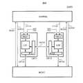
図1で示した実施形態では、メイン回路MCKTが、チップカーネルCHPKNLの管理下のもとで、サブ回路CKT1〜CKTnを使用していた。本実施例では、各サブ回路CKT1〜CKTnの使用権をもつ回路もまた電力制御の対象となる点で第1の実施形態と相違する。この実施形態を図6に示す。<Second Embodiment>
In the embodiment shown in FIG. 1, the main circuit MCKT uses the sub-circuits CKT1 to CKTn under the control of the chip kernel CHPKNL. This embodiment is different from the first embodiment in that a circuit having the right to use each of the sub-circuits CKT1 to CKTn is also subject to power control. This embodiment is shown in FIG.
CKT1〜CKT4はサブ回路である。サブ回路CKT3は、サブ回路CKT2とサブ回路CKT4を用いてある機能を実現する。また、サブ回路CKT2は、サブ回路CKT1を用いてある機能を実現する。すなわち、サブ回路CKT3はサブ回路CKT2,CKT4の使用権をもち、サブ回路CKT2はサブ回路CKT1の使用権を有する。また、各サブ回路の使用許可は、図1の実施例の場合と同様に、チップカーネルCHPKNLが統括的に行っている。 CKT1 to CKT4 are sub-circuits. The sub circuit CKT3 realizes a function using the sub circuit CKT2 and the sub circuit CKT4. Further, the sub circuit CKT2 realizes a function using the sub circuit CKT1. That is, the sub circuit CKT3 has the right to use the sub circuits CKT2 and CKT4, and the sub circuit CKT2 has the right to use the sub circuit CKT1. In addition, as in the case of the embodiment of FIG. 1, the chip kernel CHPKNL performs the use permission of each sub-circuit in a centralized manner.
本実施形態の別の特徴として、図1で存在していたチップカーネルCHPKNLによって電力が制御されないメイン回路MCKTが存在しない。メイン回路MCKTがない場合には、電源投入時のサブ回路の状態を全て図3で示されるSLP状態にすると、どの回路も動作しないために起動がかからない(永遠にチップが動作を始めない)という問題が生ずる。この問題を回避するためには、例えば電源投入時にACT状態になるサブ回路(以下、ブート回路と呼ぶ)を予め決定しておけばよい。図6に示した構成例においてはブート回路はサブ回路CKT3である。図に示す通り、ブート回路CKT3に対するリクエスト線REQS、アクノレッジ線ACKSは存在しない。電源の投入後、電力制御信号CTLS3によりブート回路CKT3が起動される。ブート回路CKT3は起動後においては、必要に応じて使用権をもつサブ回路CKT2やサブ回路CKT4を起動して所定の機能を実現する。このとき、リクエスト線REQS、アクノレッジ線ACKSによりチップカーネルCHPKNLからサブ回路の使用許可を得る必要があるのは第1の実施の形態と同様である。また、サブ回路CKT2がサブ回路CKT1を使用する場合も同様である。 As another feature of the present embodiment, there is no main circuit MCKT whose power is not controlled by the chip kernel CHPKNL that existed in FIG. When there is no main circuit MCKT, if all the sub-circuit states at the time of power-on are set to the SLP state shown in FIG. 3, it does not start because no circuit operates (the chip does not start operating forever). Problems arise. In order to avoid this problem, for example, a sub-circuit (hereinafter referred to as a boot circuit) that enters an ACT state when the power is turned on may be determined in advance. In the configuration example shown in FIG. 6, the boot circuit is the sub-circuit CKT3. As shown in the figure, there is no request line REQS or acknowledge line ACKS for the boot circuit CKT3. After the power is turned on, the boot circuit CKT3 is activated by the power control signal CTLS3. After the boot circuit CKT3 is activated, the boot circuit CKT3 activates the sub-circuit CKT2 and the sub-circuit CKT4 that have the right to use as necessary to realize a predetermined function. At this time, as in the first embodiment, it is necessary to obtain permission to use the subcircuit from the chip kernel CHPKNL by the request line REQS and the acknowledge line ACKS. The same applies when the sub circuit CKT2 uses the sub circuit CKT1.
ここで、使用権を持つ回路(例えば、サブ回路CKT3)を上位の回路、上位の回路に使用される回路(例えばサブ回路CKT3に対してサブ回路CKT2)を下位の回路と定義すると、ブート回路は最上位の回路(すなわち、該サブ回路を使用するサブ回路が存在しないサブ回路)とすることが望ましい。言い換えれば、ブート回路が直接に(例えば、サブ回路CKT2)または間接に(例えば、サブ回路CKT1)使用することのできない回路については、チップカーネルCHPKNLによる電力制御は適用できない。 Here, if a circuit having a usage right (for example, sub circuit CKT3) is defined as a higher circuit, and a circuit used for the upper circuit (for example, sub circuit CKT2 with respect to sub circuit CKT3) is defined as a lower circuit, a boot circuit is defined. Is preferably a top-level circuit (that is, a sub-circuit in which no sub-circuit using the sub-circuit exists). In other words, power control by the chip kernel CHPKNL cannot be applied to a circuit that cannot be used directly (for example, the subcircuit CKT2) or indirectly (for example, the subcircuit CKT1) by the boot circuit.
なお、図1や図6の構成に限らず、サブ回路CKTとメイン回路MCKTの構成は数々の構成が可能である。例えば、メイン回路MCKTを有する構成において、サブ回路CKTを図6のように階層的に構成しても良い。また、上位の回路と下位の回路とは1対1の関係にある必要はなく、1対多、多対1の関係にあってもよい。 Note that the configurations of the sub circuit CKT and the main circuit MCKT are not limited to the configurations of FIGS. For example, in the configuration having the main circuit MCKT, the sub-circuit CKT may be hierarchically configured as shown in FIG. Further, the upper circuit and the lower circuit need not have a one-to-one relationship, and may have a one-to-many or many-to-one relationship.
<第3の実施の形態>
図1や図6に示されるリクエスト線REQS1〜REQSn、アクノレッジ線ACKS1〜ACKSn、電力制御線CTLS1〜CTLSnの物理的な形態や論理的な形態は特に限定しない。<Third Embodiment>
The physical form and logical form of the request lines REQS1 to REQSn, acknowledge lines ACKS1 to ACKSn, and power control lines CTLS1 to CTLSn shown in FIGS. 1 and 6 are not particularly limited.
物理的な形態として図2の構成例では、電力制御線CTLS1〜CTLSnはそれぞれ3本の配線CTLSa, CTLSb, CTLScで構成されている。このようにパラレルに電力制御信号を伝送するのではなく、シリアルに伝送することにより1本の配線で電力制御することも可能である。もちろん、電力制御の種類を限定すれば配線数は少なくて済む。 As a physical form, in the configuration example of FIG. 2, the power control lines CTLS1 to CTLSn are each configured by three wirings CTLSa, CTLSb, and CTLSc. In this way, it is possible to control power with a single wire by transmitting serially instead of transmitting the power control signal in parallel. Of course, if the types of power control are limited, the number of wires can be reduced.
リクエスト線REQS1〜REQSnについても同様である。状態遷移が1種類に限定されていれば(例えばACT状態とSTB状態のみ)、1ビットのリクエスト信号を1本のリクエスト線により伝達することができる。図4の実施例で示したように3つ以上の状態があり、遷移する先が複数ありうる場合には、2ビット以上のリクエスト信号をビット数に応じた複数の配線を用いて各状態への遷移を要求できるようにしてもよい。またさらに、各状態への遷移を要求する際、その遷移の優先度を指定できるようにすることも望ましい。サブ回路スケジューリングは、その優先度にしたがってサブ回路の電力遷移を制御する。チップカーネルCHPKNLは、優先度の高い要求に対して優先的に使用許可を出し、リソースの使用効率が向上する。 The same applies to the request lines REQS1 to REQSn. If the state transition is limited to one type (for example, only ACT state and STB state), a 1-bit request signal can be transmitted through one request line. As shown in the embodiment of FIG. 4, when there are three or more states and there can be a plurality of transition destinations, a request signal of 2 bits or more is sent to each state using a plurality of wirings according to the number of bits. May be requested. It is also desirable to be able to specify the priority of the transition when requesting a transition to each state. The sub circuit scheduling controls the power transition of the sub circuit according to the priority. The chip kernel CHPKNL gives priority to use of a request with a high priority, thereby improving resource use efficiency.
リクエスト線REQS1〜REQSn、アクノレッジ線ACKS1〜ACKSn、電力制御線CTLS1〜CTLSnは、まとめてバス構造(以下、電力制御バスと呼ぶ)にして各サブ回路に接続してもよい。サブ回路の数が多い場合には、配線に要する面積を小さくすることができ、当然バス構造の方が拡張性にも優れる。この場合、一つのバス構造に対する、複数のアクセスの競合を回避する必要がある。リクエスト信号REQSは各サブ回路から任意のタイミングで出力されるため、リクエスト線REQS1〜REQSnについては一つの共通するバスで共用できない。ラウインドロビン方式やトークンリング方式を採用する場合、リクエスト信号の到達が遅れる回路が生じるが、設計時の拡張性が高い。あるいは、アクノレッジ線ACKS、電力制御線はCTLSは共通バスにまとめ、リクエスト線REQSはポイント・ツウ・ポイント方式によって接続してもよい。この場合は、どの回路もリクエスト信号が平等にかつ高速にチップカーネルCHPKNLに到達する。 The request lines REQS1 to REQSn, acknowledge lines ACKS1 to ACKSn, and power control lines CTLS1 to CTLSn may be collectively connected to each subcircuit in a bus structure (hereinafter referred to as a power control bus). When the number of sub-circuits is large, the area required for wiring can be reduced, and the bus structure is naturally superior in expandability. In this case, it is necessary to avoid contention for multiple accesses to one bus structure. Since the request signal REQS is output from each sub circuit at an arbitrary timing, the request lines REQS1 to REQSn cannot be shared by one common bus. When the wind robin method or the token ring method is adopted, a circuit in which the arrival of the request signal is delayed occurs, but the extensibility at the time of design is high. Alternatively, the acknowledge line ACKS and the power control line may be combined into a common bus for CTLS, and the request line REQS may be connected by a point-to-point method. In this case, the request signal reaches the chip kernel CHPKNL equally and at high speed in any circuit.
また、電力制御バスとして、従来からチップ内に存在している信号伝播用のオンチップバス(例えば、英国ARM社のAdvanced Microcontroller Bus Architecture (SMBA)などが挙げられる)と一部あるいは全ての信号線を共用することも可能である。 In addition, the power control bus includes an on-chip bus for signal propagation that has traditionally existed in the chip (for example, Advanced Microcontroller Bus Architecture (SMBA) of ARM UK) and some or all signal lines. Can also be shared.
<第4の実施の形態>
チップ許容電力Pmaxは、チップの製造時や設計時に決定し、その後は変更しないようにしてもよいし、チップの製造後に変更できるようにしてもよい。変更できるようにするためには、Pmaxをチップ上に集積した不揮発性メモリに格納しておいてもよい。あるいはチップの電源投入時にチップ外部からPmaxの値を読み込むようにしてもよい。また、チップのボンティング仕様やチップ上に形成された配線によるジャンパ切り替えによって決定するようにしてもよい。その他、様々な方法が考えられるがその手法は特に限定しない。<Fourth embodiment>
The chip allowable power Pmax is determined at the time of manufacturing or designing the chip, and may not be changed thereafter, or may be changed after the manufacturing of the chip. In order to be able to change, Pmax may be stored in a non-volatile memory integrated on the chip. Alternatively, the value of Pmax may be read from the outside of the chip when the chip is powered on. Further, it may be determined by the bonding specification of the chip or jumper switching by the wiring formed on the chip. Various other methods are conceivable, but the method is not particularly limited.
チップ許容電力Pmaxをその設計後に変更できるようにすることで、同じ回路を集積したチップであっても、その実装するパッケージごとに異なる許容電力Pmaxを設定できる。一般に、安価なプラスティックパッケージを用いた場合には、熱抵抗が大きく耐熱性が悪いためにチップの消費電力の許容上限が低い。このような場合には、Pmaxの値を小さくすればよい。また逆に、高価なセラミックパッケージを用いた場合には、Pmaxの値を高くすることができる。Pmaxの値を高く設定すればそれだけ多くのサブ回路を同時に動作させることができるためにチップ性能を向上させることができる。パッケージごとに異なるPmaxを設定することで、チップの性能をパッケージに応じて設定できる。 By allowing the chip allowable power Pmax to be changed after the design, even if the chip has the same circuit integrated, a different allowable power Pmax can be set for each package to be mounted. In general, when an inexpensive plastic package is used, the allowable upper limit of power consumption of the chip is low because the thermal resistance is large and the heat resistance is poor. In such a case, the value of Pmax may be reduced. Conversely, when an expensive ceramic package is used, the value of Pmax can be increased. If the value of Pmax is set high, more subcircuits can be operated at the same time, so that the chip performance can be improved. By setting different Pmax for each package, the chip performance can be set according to the package.
このようにパッケージの種類に応じてPmaxの値を異ならせることにより、高速バージョンのチップと低電力バージョンのチップが、回路設計を共通にして開発コストを抑制しつつ実現でき、安価かつ容易に多くの品種展開ができる。図7にPmaxの値を図5の実施例の場合よりも小さく設定し、サブ回路の消費電力の合計を150mWに設定した場合の、図5とは異なるサブ回路スケジューリングの実施例を示す。図5では、時刻5で200mWの電力を消費していたが、図7の実施例ではCKT1とCKT4のACT状態への遷移が延期され、結果的に150mW以下で動作が推移している。たとえば、図5を高速バージョンのサブ回路スケジューリングとすれば、図7は低電力バージョンのチップにおけるサブ回路スケジューリングに相当する。このように処理性能と消費電力のバランスを要求されるチップの仕様に応じて変化させることができる。 In this way, by varying the value of Pmax according to the type of package, high-speed version chips and low-power version chips can be realized while reducing development costs by sharing circuit design, and many cheap and easy Varieties can be developed. FIG. 7 shows an example of sub-circuit scheduling different from FIG. 5 in the case where the value of Pmax is set smaller than that in the example of FIG. 5 and the total power consumption of the sub-circuits is set to 150 mW. In FIG. 5, 200 mW of power was consumed at
また、設計後のPmaxの変更は、チップを異なる製造プロセスで作りなおした場合にも有効である。製造プロセスごとに最適なPmaxが設定できる。 Moreover, the change in Pmax after design is also effective when the chip is remade by a different manufacturing process. The optimum Pmax can be set for each manufacturing process.
さらに、チップ許容電力Pmaxは、チップの電源投入後に動的に変化させてもよい。例えば、Pmaxの値をチップの温度に応じて変化させる。チップ温度が高くなればPmaxを小さくし、チップ温度が低くなればPmaxを大きくする。時間的な遅延はあるものの、チップの温度は消費電力と対応する(Tj=Ta+θ×W(Tj:ジャンクション温度、Ta:周辺温度、θ:パッケージの熱抵抗、W:消費電力))ため、本発明によってチップの温度を管理できる。 Further, the chip allowable power Pmax may be dynamically changed after the chip is powered on. For example, the value of Pmax is changed according to the temperature of the chip. If the chip temperature increases, Pmax decreases, and if the chip temperature decreases, Pmax increases. Although there is a time delay, the chip temperature corresponds to the power consumption (Tj = Ta + θ x W (Tj: junction temperature, Ta: ambient temperature, θ: package thermal resistance, W: power consumption)). The invention can control the temperature of the chip.
また、本発明のチップを電池で駆動している場合には、電池残量によってPmaxの設定値を変化させてもよい。電池残量が多い場合やACコンセントから給電されている場合にはPmaxを大きくする。電池残量が少なくなったらPmaxを小さくする。あるいはACコンセントからの給電が停止された場合にPmaxを小さくしてもよい。電池駆動時間を長くできる。 In addition, when the chip of the present invention is driven by a battery, the set value of Pmax may be changed depending on the remaining battery level. When the remaining battery level is high or when power is supplied from an AC outlet, Pmax is increased. When the battery level is low, decrease Pmax. Alternatively, Pmax may be reduced when power supply from the AC outlet is stopped. Battery drive time can be extended.
<第5の実施の形態>
各サブ回路の消費電力を考慮してサブ回路スケジューリングを行うためには、チップカーネルCHPKNLは図3で示したように、各サブ回路の各状態における消費電力量を把握している必要がある。把握する方法としては、数々の方法が考えられるが、本発明では特にその方法は限定しない。例えば、チップの設計時に図3の表をチップカーネルCHPKNL内に格納してもよい。また、各サブ回路に各状態時の電力情報を格納し、電源投入時等に、チップカーネルCHPKNLが特定のプロトコルに従ってその電力情報を各サブ回路から読み出してもよい。<Fifth embodiment>
In order to perform subcircuit scheduling in consideration of the power consumption of each subcircuit, the chip kernel CHPKNL needs to grasp the power consumption in each state of each subcircuit as shown in FIG. A number of methods are conceivable as a method of grasping, but the method is not particularly limited in the present invention. For example, the table of FIG. 3 may be stored in the chip kernel CHPKNL at the time of chip design. Further, power information in each state may be stored in each sub circuit, and the chip kernel CHPKNL may read the power information from each sub circuit according to a specific protocol when the power is turned on.
<第6の実施の形態>
サブ回路スケジューリングは、チップカーネルCHPKNLがリクエスト線REQSを介してサブ回路の使用許可申請を受けてから、なるべく早くにアクノレッジ線ACKSを介して使用許可を与えた方が、チップの処理性能が高くなる。一つの方法としては、状態遷移に時間を要するものについてはそのような状態遷移がなるべく避けるようにスケジューリングする。例えば、図4の状態遷移図の例ではSLP状態への遷移はなるべく避けるようにスケジューリングする。これは、SLP状態からACT状態またはSTB状態への遷移は電源のオンが伴い、電源のオンを伴わないSTB状態からACT状態への遷移と比べて多くの時間を要するためである。このようなスケジューリングを実現するためには、ACT状態(またはSTB状態)からSLP状態に遷移するために経由する中間状態をACT状態からSTB状態に遷移するために経由する中間状態を多く設ければよい。しかし、SLP状態をなるべく使わない方法では、電力の削減効果が小さくなるという課題がある。<Sixth Embodiment>
For subcircuit scheduling, the chip kernel CHPKNL receives a request for permission to use the subcircuit via the request line REQS, and then the chip processing performance is higher when the permission is granted via the acknowledge line ACKS as soon as possible. . As one method, scheduling is performed so as to avoid such state transitions as much as possible for those that require time for state transitions. For example, in the example of the state transition diagram of FIG. 4, scheduling is performed so as to avoid the transition to the SLP state as much as possible. This is because the transition from the SLP state to the ACT state or the STB state involves turning on the power supply and requires more time than the transition from the STB state to which the power supply is not turned on to the ACT state. In order to realize such scheduling, it is necessary to provide many intermediate states to transit from the ACT state (or STB state) to the SLP state to transit from the ACT state to the STB state. Good. However, the method that does not use the SLP state as much as possible has a problem that the power reduction effect is reduced.
電力の削減効果を高めるため、サブ回路が実際に必要になる時刻よりも前に、チップカーネルCHPKNLにそのサブ回路の使用許可予定の申請をしてもよい。チップカーネルCHPKNLはこの使用許可予定の申請を受け取ると、引き続いて使用許可申請がなされたときに、すぐに使用許可を与えられるようにサブ回路の状態をスケジューリングする。このサブ回路スケジューリングによって、チップカーネルCHPKNLがサブ回路の使用許可申請を受けてから使用許可を与えるまでの時間を短くすることができ、チップの処理性能を高くできる。例えば、ある機能を実現するために必要なサブ回路についてあらかじめ使用許可予定の申請によってSLP状態からSTB状態に遷移させておく。その後、サブ回路を使用するときに使用許可の申請によってSTB状態からACT状態に遷移させることで、許可申請がなされた後に比較的早くにサブ回路を使用することができる。 In order to increase the power reduction effect, an application for permission to use the subcircuit may be submitted to the chip kernel CHPKNL before the time when the subcircuit is actually needed. When the chip kernel CHPKNL receives the application for the use permission schedule, it schedules the state of the sub-circuit so that the use permission can be given immediately when the use permission application is subsequently made. This sub-circuit scheduling can shorten the time from when the chip kernel CHPKNL receives a sub-circuit usage permission application to when the chip kernel CHPKNL receives a permission to use, thereby increasing the processing performance of the chip. For example, a sub-circuit necessary for realizing a certain function is changed from the SLP state to the STB state in advance by applying for a use permission schedule. Thereafter, when the sub circuit is used, the sub circuit can be used relatively early after the permission application is made by making the transition from the STB state to the ACT state by applying for the use permission.
<第7の実施の形態>
図2では、NMOSトランジスタMN2(電源スイッチ)を用いてサブスレッショルドリーク電流を制御している。しかし、低消費電力化するための回路構成は図2に示すものに限られない。電源回路を内蔵し、その電源電圧を変化させる方式でもよい。前記のようにCMOS回路の動作時消費電力は電源電圧の2乗に比例するため、低い電源電圧(例えば0.5V)と高い電源電圧(例えば1.2V)で動作する少なくとも二つの状態を設けることでも回路LGの電力を制御できる。<Seventh embodiment>
In FIG. 2, the NMOS transistor MN2 (power switch) is used to control the subthreshold leakage current. However, the circuit configuration for reducing power consumption is not limited to that shown in FIG. A method of incorporating a power supply circuit and changing the power supply voltage may be used. Since the power consumption during operation of the CMOS circuit is proportional to the square of the power supply voltage as described above, it is also possible to provide at least two states that operate at a low power supply voltage (for example, 0.5 V) and a high power supply voltage (for example, 1.2 V). The power of the circuit LG can be controlled.
図2の実施例では、MOSトランジスタMN2をオフ状態にしてしまうと、回路LG内のフリップフロップ等の情報記憶素子に格納されている情報が消去されてしまう。これを防ぐ一つの方法として、MOSトランジスタMN2がオフ状態でも上記情報を保持するためのレベルホルダ回路を付加する。例えば、このレベルホルダ回路は、正の電源線VDDと負(グランド)の電源線VSSとの間で動作し、比較的低い駆動力のトランジスタで構成されるラッチ回路として実現できる。また、上記のようにサブ回路の電源電圧として、低い電源電圧と高い電源電圧で動作する少なくとも二つの状態を設ける場合には、低い電源電圧の状態時にサブ回路に与える電源電圧を、サブ回路内のフリップフロップ等の情報記憶素子に格納されている情報が消去されないような電圧値とする(情報が保持できないような低い電圧値にしない)。かかる構成では、レベルホルダ回路が不要になるという効果がある。また、そのような電圧であれば、高い電源電圧の状態への遷移が高速にでき、さらにその遷移に要する電力消費が少なくて済むという効果もある。 In the embodiment of FIG. 2, if the MOS transistor MN2 is turned off, information stored in an information storage element such as a flip-flop in the circuit LG is erased. As one method for preventing this, a level holder circuit for holding the above information is added even when the MOS transistor MN2 is off. For example, the level holder circuit operates between the positive power supply line VDD and the negative (ground) power supply line VSS, and can be realized as a latch circuit including transistors having a relatively low driving capability. Further, when providing at least two states that operate with a low power supply voltage and a high power supply voltage as the power supply voltage of the subcircuit as described above, the power supply voltage applied to the subcircuit in the low power supply voltage state is set in the subcircuit. The voltage value is such that information stored in an information storage element such as a flip-flop is not erased (the voltage value is not so low that information cannot be retained). With such a configuration, there is an effect that a level holder circuit becomes unnecessary. In addition, such a voltage has an effect that a transition to a high power supply voltage state can be performed at a high speed, and power consumption required for the transition can be reduced.
また、図2ではANDゲートG1を用いて回路LGに伝播されるクロックのオン・オフを制御している。いわば、図2の制御方法はクロックを所定の周波数のクロック発振と周波数が0のクロック発振とを切り替えているともいえる。これに対して、クロックCLKの周波数を変化させる手段(例えば分周器やフェーズ・ロックド・ループ(PLL)回路)をANDゲートG1の代わりに設置してもよい。前記のようにCMOS回路の動作時消費電力は動作周波数に比例するため、低い動作周波数(例えば10MHz)と高い動作周波数(例えば200MHz)で動作する少なくとも二つの状態を設けることでも回路LGの電力を制御できる。 In FIG. 2, the on / off of the clock propagated to the circuit LG is controlled using the AND gate G1. In other words, it can be said that the control method of FIG. 2 switches the clock oscillation between a clock oscillation having a predetermined frequency and a clock oscillation having a frequency of 0. On the other hand, means for changing the frequency of the clock CLK (for example, a frequency divider or a phase-locked loop (PLL) circuit) may be provided instead of the AND gate G1. Since the power consumption during operation of the CMOS circuit is proportional to the operating frequency as described above, the power of the circuit LG can be reduced by providing at least two states that operate at a low operating frequency (for example, 10 MHz) and a high operating frequency (for example, 200 MHz). Can be controlled.
図8はこのような多様な電力制御を実現できるサブ回路の構成を示したものである(図1を元にした構成例であるが、図6についてもサブ回路は同様の構成になる)。サブ回路CKT1とCKT2はそれぞれ、電力制御回路PWC1、PWC2と、サブ回路の機能を実現する回路LG1、LG2と、サブ回路の外部との通信を行うインターフェース回路IFC1、IFC2とで構成されている。 FIG. 8 shows a configuration of a sub circuit capable of realizing such various power controls (a configuration example based on FIG. 1, but the sub circuit has the same configuration also in FIG. 6). Each of the sub-circuits CKT1 and CKT2 includes power control circuits PWC1 and PWC2, circuits LG1 and LG2 that realize the function of the sub-circuit, and interface circuits IFC1 and IFC2 that communicate with the outside of the sub-circuit.
電力制御回路PWCは、上記のような方法を用いて、サブ回路の負荷の充放電による電力消費とリーク電流による電力消費を、チップカーネルCHPKNLからの電力制御線CTLSの指示にしたがって制御する。上記の電源回路やPLL回路等のクロック周波数可変回路が、電力制御回路PWCの具体的な構成例である。 The power control circuit PWC uses the above-described method to control power consumption due to charging / discharging of the load of the sub circuit and power consumption due to leakage current in accordance with an instruction of the power control line CTLS from the chip kernel CHPKNL. The clock frequency variable circuit such as the power supply circuit and the PLL circuit is a specific configuration example of the power control circuit PWC.
また、上記のようにサブ回路内の回路LGに供給する電源電圧をサブ回路毎に異なる値にして、サブ回路の電力を制御する場合には、それらのサブ回路CKT間あるいはサブ回路CKTとメイン回路MCKT間でのインターフェースを行う回路が必要となる。電源電圧値の異なるCMOS回路をそのまま接続すると貫通電流等のリーク電流が流れるからである。インターフェース回路IFCはこれらの貫通電流を防ぐために設置する。電源電圧の異なるサブ回路のインターフェース回路IFCに好ましいレベル変換回路の構成例が、特開平11-195975号公報に開示されている。 Further, when the power supply voltage supplied to the circuit LG in the sub-circuit is set to a different value for each sub-circuit and the power of the sub-circuit is controlled as described above, between the sub-circuits CKT or the sub-circuit CKT and the main circuit. A circuit for interfacing between the circuits MCKT is required. This is because leakage current such as through current flows when CMOS circuits having different power supply voltage values are connected as they are. The interface circuit IFC is installed to prevent these through currents. Japanese Patent Laid-Open No. 11-195975 discloses a configuration example of a level conversion circuit suitable for the interface circuit IFC of sub-circuits having different power supply voltages.
なお、図2の構成例と図8の構成例との対応は次の通りである。ANDゲートG2及びG3がインターフェース回路IFCに相当し、NMOSトランジスタNM2及びANDゲートG1が電力制御回路PWCに相当する。 The correspondence between the configuration example of FIG. 2 and the configuration example of FIG. 8 is as follows. The AND gates G2 and G3 correspond to the interface circuit IFC, and the NMOS transistor NM2 and the AND gate G1 correspond to the power control circuit PWC.
<第9の実施の形態>
図9にチップカーネルCHPKNLの構成例を示す。バッファBUF1〜BUFnは電力制御線CTLSの駆動回路である。シーケンサSEQ1〜SEQnは図4の例に示したような状態遷移を実現する。電力テーブルPWRTABは、図3の例に示したような各動作状態時の電力値や、各動作状態遷移に必要な電力の値(エネルギー値でも可)が格納されている。バッファBUF1〜BUFnを構成するドライバC1〜C3については第1の実施の形態において説明した。シーケンサSEQ1〜SEQnとバッファBUF1〜BUFnによって、電力制御モジュールPCM1〜PCMnが構成され、各サブ回路毎の動作状態が管理されている。<Ninth embodiment>
FIG. 9 shows a configuration example of the chip kernel CHPKNL. The buffers BUF1 to BUFn are drive circuits for the power control line CTLS. The sequencers SEQ1 to SEQn realize state transition as shown in the example of FIG. The power table PWRTAB stores a power value in each operation state as shown in the example of FIG. 3 and a power value (may be an energy value) necessary for each operation state transition. The drivers C1 to C3 constituting the buffers BUF1 to BUFn have been described in the first embodiment. The power control modules PCM1 to PCMn are configured by the sequencers SEQ1 to SEQn and the buffers BUF1 to BUFn, and the operation state of each subcircuit is managed.
電力アービタARBITは、各電力制御モジュールPCM1〜PCMn中の電力テーブルPWRTABの値を参照しながら、上記のサブ回路スケジューリングにしたがって各サブ回路の動作状態を制御している。このように、各サブ回路CKT1〜CKTnに対する電力制御は各電力制御モジュールPCM1〜PCMnが行い、電力アービタARBITは、各サブ回路CKT1〜CKTn間での電力消費の調整を行うことで、サブ回路スケジューリングに必要な処理を階層で分散することができ、各階層の設計が容易になるという効果がある。 The power arbiter ARBIT controls the operating state of each sub-circuit according to the above-mentioned sub-circuit scheduling while referring to the value of the power table PWRTAB in each power control module PCM1 to PCMn. As described above, the power control for each subcircuit CKT1 to CKTn is performed by each power control module PCM1 to PCMn, and the power arbiter ARBIT adjusts the power consumption among the subcircuits CKT1 to CKTn, thereby subcircuit scheduling. The processes necessary for the above can be distributed in the hierarchy, and the design of each hierarchy is facilitated.
上記した各サブ回路CKTの動作状態遷移頻度を制約する回路は、電力制御モジュールPCM1〜PCMnで実現する。また、別の例では、サブ回路CKTがある一定以上の時間使用されなかった場合には、そのサブ回路に対応した電力制御モジュールPCMが、電力アービタARBITとは独立して、そのサブ回路の動作状態をより低電力な動作状態になるように変更し、変更後の状態及びその電力消費量を電力アービタARBITに通知する。これにより電力アービタARBITに多くの処理負荷を負わすことなく、チップの消費電力を効率的に削減するサブ回路スケジューリングが実現できる。 The circuit that restricts the operation state transition frequency of each of the sub-circuits CKT described above is realized by the power control modules PCM1 to PCMn. In another example, when the sub circuit CKT has not been used for a certain period of time, the power control module PCM corresponding to the sub circuit operates the sub circuit independently of the power arbiter ARBIT. The state is changed to a lower power operation state, and the changed state and its power consumption are notified to the power arbiter ARBIT. As a result, it is possible to realize sub-circuit scheduling that efficiently reduces the power consumption of the chip without imposing a large processing load on the power arbiter ARBIT.
<第10の実施の形態>
図10は、本発明のチップ電力制御を実現する半導体装置の設計フローを示す。ライブラリLG_LIB1は、サブ回路CKTの機能を実現する回路が格納されたライブラリである。すなわち、図9の実施例で示したサブ回路CKTの電力制御モジュールPCMが付加されていないものである。ライブラリPCM_LIB1はLG_LIB1中のサブ回路CKTに対応する電力制御モジュールPCMが格納されたライブラリである。ライブラリLG_LIB2もサブ回路CKTのライブラリであるが、格納されているサブ回路には電力制御モジュールPCMが既に付加されている。ライブラリMC_LIBは図1の実施例で示したメイン回路MCKTが格納されたライブラリである。<Tenth Embodiment>
FIG. 10 shows a design flow of a semiconductor device that realizes chip power control according to the present invention. The library LG_LIB1 is a library in which a circuit that realizes the function of the sub circuit CKT is stored. That is, the power control module PCM of the sub circuit CKT shown in the embodiment of FIG. 9 is not added. The library PCM_LIB1 is a library in which the power control module PCM corresponding to the sub circuit CKT in LG_LIB1 is stored. The library LG_LIB2 is also a library of the subcircuit CKT, but the power control module PCM is already added to the stored subcircuit. The library MC_LIB is a library in which the main circuit MCKT shown in the embodiment of FIG. 1 is stored.
LG_LIB1、PCM_LIB1、LG_LIB2、MC_LIBで示された4つのライブラリと、チップカーネルCHPKNLは、例えばその機能がHDL(Hardware Description Language)等の言語でその回路の機能を記述したデータとして格納される。論理合成用セルライブラリCELL_LIBには、論理合成に用いられる各種セル(例えば、AND、OR等の論理ゲートまたは複合論理ゲートのセル)の情報(例えば、各種セルの遅延時間情報)が格納される。設計者はチップ全体に係る論理仕様RTL(特に限定しないが、ここではレジスタ・トランスファ・レベル(RTL:Registor Transfer Level)で記述されているものと仮定した)を作成し、論理仕様RTL、ライブラリに格納された回路データ及びセルの情報からネットリストNETLSTを論理合成(LOG_SYN)する。ネットリストNETLSTはその後、レイアウトされる(LAY)。 The four libraries indicated by LG_LIB1, PCM_LIB1, LG_LIB2, and MC_LIB and the chip kernel CHPKNL are stored, for example, as data describing the function of the circuit in a language such as HDL (Hardware Description Language). The logic synthesis cell library CELL_LIB stores information (for example, delay time information of various cells) of various cells (for example, logic gates such as AND and OR, or complex logic gate cells) used for logic synthesis. The designer creates a logical specification RTL for the entire chip (although it is not limited, it is assumed here that it is described in Register Transfer Level (RTL)). The netlist NETLST is logically synthesized (LOG_SYN) from the stored circuit data and cell information. The netlist NETLST is then laid out (LAY).
上記設計フローによって、そのままでは本発明の電力制御が適用できないようなサブ回路(ライブラリLG_LIB1に格納されたサブ回路)でも、電力制御モジュールPCMを付加することで、本発明の電力制御が適用できるようになる。いわゆるIPプロバイダの供給する多くのIP(Intellectual Property:半導体集積回路に設けられる演算機能や信号制御機能等の機能上のまとまりを単位とする回路ブロック)をチップ設計に取り込むことができ、効率的な設計が可能になる。 According to the above design flow, the power control of the present invention can be applied by adding the power control module PCM even to a sub circuit (a sub circuit stored in the library LG_LIB1) where the power control of the present invention cannot be applied as it is. become. Efficient IP (Intellectual Property: supplied by an IP provider) can be incorporated into the chip design by incorporating into the chip design a circuit block based on functional units such as arithmetic functions and signal control functions provided in semiconductor integrated circuits. Design becomes possible.
電力制御モジュールPCMは各サブ回路毎に作成する必要がある。このためには、電力アービタARBITと電力制御モジュールPCMの間のインターフェース仕様(以下、PSI(Power Scheduling Interface)と呼ぶ)に基づき設計する。PSIには、電力アービタARBITからのコマンドとそのコマンドに対する電力制御モジュールの応答のプロトコルが含まれる。 The power control module PCM needs to be created for each subcircuit. For this purpose, the design is based on an interface specification between the power arbiter ARBIT and the power control module PCM (hereinafter referred to as PSI (Power Scheduling Interface)). The PSI includes a protocol from the power arbiter ARBIT and a response of the power control module to the command.
同様に、論理仕様RTLを設計する設計者は、電力制御モジュールPCMとサブ回路ブロックCKTの間のインターフェース仕様(以下、PMI(Power Managing Interface)と呼ぶ。PMIには、メイン回路MKCTまたはサブ回路ブロックCKTからのリクエスト信号REQSとチップカーネルCHPKNLからのアクノレッジ信号REQSとのプロトコルが含まれる。)を把握し、リクエスト信号REQSとアクノレッジ信号ACKSで制御される各サブ回路を用いた設計ができる。 Similarly, a designer who designs the logical specification RTL is an interface specification (hereinafter referred to as PMI (Power Managing Interface) between the power control module PCM and the sub circuit block CKT. The PMI includes a main circuit MKCT or a sub circuit block. This includes the protocol of the request signal REQS from the CKT and the acknowledge signal REQS from the chip kernel CHPKNL), and can be designed using each sub-circuit controlled by the request signal REQS and the acknowledge signal ACKS.
インターフェース仕様PMIとPSIに基づき、既存の回路ブロックの設計を利用して本発明の電力制御を容易に実現することができる。 Based on the interface specifications PMI and PSI, the power control of the present invention can be easily realized by utilizing the existing circuit block design.
<第11の実施の形態>
図11は、本発明の電力制御を用いたチップ(CHP3)の実施例を示した図である。チップ内の信号伝播用のオンチップバスSBUSに、マイクロプロセッサ(Central Processing Unit)CPU、Long Instruction word方式のマイクロプロセッサVLIW、デジタル信号処理プロセッサ(Degital signal processor)DSP、グラフィックプロセッサ(Graphic processor)GP、MPEG(Moving Picture Experts Group)信号処理回路MPEG、バス制御回路BSC、チップ電力制御回路PMU、USB(Universal Sirial Bus)インターフェース回路USB、IrDA(Infrared Data Association)赤外線通信インターフェース回路IrDA、IEEE1394インターフェース回路IEEE1394、PCI(Peripheral Component Interconnect)インターフェース回路PCI、メモリMEMが接続されている。EXTBUSは外部バスであって、バスコントローラBSCを介してオンチップバスSBUSと接続される。CHP3は、CPU、VLIW、DSP、GP、MPEG等の専用回路とメモリMEMを用いてデータ処理を行い、USB、IrDA、IEEE1394、PCI、BSCを用いてチップ外部とのデータの授受を行う。もちろんこれらの回路ブロックは例示であって、チップCHP3の用途に応じて必要な回路ブロックを搭載する。また、電力制御バスPBUSは本発明の電力制御を実施するためのものである。<Eleventh embodiment>
FIG. 11 is a diagram showing an embodiment of a chip (CHP3) using the power control of the present invention. On-chip bus SBUS for signal propagation within the chip, microprocessor (Central Processing Unit) CPU, Long Instruction word type microprocessor VLIW, digital signal processor (Degital signal processor) DSP, graphic processor (Graphic processor) GP, MPEG (Moving Picture Experts Group) signal processing circuit MPEG, bus control circuit BSC, chip power control circuit PMU, USB (Universal Sirial Bus) interface circuit USB, IrDA (Infrared Data Association) infrared communication interface circuit IrDA, IEEE1394 interface circuit IEEE1394, A PCI (Peripheral Component Interconnect) interface circuit PCI and a memory MEM are connected. EXTBUS is an external bus and is connected to the on-chip bus SBUS via the bus controller BSC. The CHP3 performs data processing using a dedicated circuit such as a CPU, VLIW, DSP, GP, and MPEG and a memory MEM, and exchanges data with the outside of the chip using USB, IrDA, IEEE1394, PCI, and BSC. Of course, these circuit blocks are examples, and necessary circuit blocks are mounted according to the use of the chip CHP3. The power control bus PBUS is for carrying out the power control of the present invention.
チップCHP3の電力制御は以下のように行われる。チップ電力制御回路PMUはチップCHP3の電力状態を制御している回路であり、チップ外部(例えばEXTBUS)からの指示(割り込み処理等)あるいは、CPU等が実行する命令列(スタンバイ命令等)にしたがって、チップ全体の動作状態を制御する。たとえば、チップ全体を高速動作する動作状態や、低速動作する動作状態、あるいは、動作を停止させる待機状態等に制御する(以下、これらのチップ全体の動作状態をチップ動作状態と記す)。チップ電力制御回路PMUはチップカーネルCHPKNLを制御して、上記したような数々のチップ動作状態を実現する。チップ電力制御回路PMUのチップカーネルCHPKNLの制御方法は特に限定しないが、例えばチップカーネルCHPKNL のPmax値を、チップ動作状態に応じて変化させることで実現できる。また、ほとんど全ての回路モジュールはチップカーネルCHPKNLによって、本発明の方法にしたがって電力制御される。なお、チップカーネルCHPKNLは、図11に示されるように独立の回路ブロックとしてもよく、一部の回路ブロック(例えばCPU)の一部機能として実現することも可能である。 The power control of the chip CHP3 is performed as follows. The chip power control circuit PMU is a circuit that controls the power state of the chip CHP3, according to instructions from the outside of the chip (for example, EXTBUS) (interrupt processing, etc.) or a command sequence (such as a standby instruction) executed by the CPU, etc. Control the operating state of the entire chip. For example, the entire chip is controlled to an operating state in which the entire chip operates at high speed, an operating state in which the entire chip operates at low speed, or a standby state in which the operation is stopped (hereinafter, the operating state of the entire chip is referred to as a chip operating state). The chip power control circuit PMU controls the chip kernel CHPKNL to realize a number of chip operating states as described above. The method for controlling the chip kernel CHPKNL of the chip power control circuit PMU is not particularly limited. For example, it can be realized by changing the Pmax value of the chip kernel CHPKNL according to the chip operating state. Almost all circuit modules are power controlled by the chip kernel CHPKNL according to the method of the present invention. The chip kernel CHPKNL may be an independent circuit block as shown in FIG. 11, or may be realized as a partial function of a part of circuit blocks (for example, CPU).
一般に、専用回路は汎用回路よりも消費電力が小さい。専用回路は汎用回路と比較して、ある機能を実現するために無駄な回路が少ないためである。例えばMPEG処理を汎用のマイクロプロセッサで実現するよりも、MPEG処理専用の回路で実現する方が低電力である。本発明のチップでは上記した仮想集積を行えるために、図11の実施例のように多くの専用回路をチップ上に集積することができ、汎用回路ではなく専用回路で処理することにより、チップの消費電力を大幅に削減できる。 In general, a dedicated circuit consumes less power than a general-purpose circuit. This is because the dedicated circuit has fewer unnecessary circuits to realize a certain function than the general-purpose circuit. For example, it is less power to implement MPEG processing with a circuit dedicated to MPEG processing than to realize it with a general-purpose microprocessor. Since the above-described virtual integration can be performed in the chip of the present invention, a large number of dedicated circuits can be integrated on the chip as in the embodiment of FIG. Power consumption can be greatly reduced.
<第12の実施の形態>
本発明のチップは、従来のチップに比べてその消費電流変動を小さくできる。従来のチップでは、チップ全体の消費電力を考慮することなくサブ回路の電力制御を行う。そのため、電力のピーク値(熱設計電力:Thermal Design Power)は平均電力の数倍の大きさになってしまうのが通常である。これに対して本発明のチップでは、チップ全体の消費電力が予め設定されたチップ許容電力Pmaxに制限され、Pmaxの超過を生ぜしめるようなサブ回路の使用は後回しにされる。チップの消費電力に余裕が生じ、当該サブ回路を使用してもPmaxの超過を生じない状況になって初めて、当該サブ回路の使用が許可される。すなわち、本発明の電力制御は、いわば従来のチップにみられた電力消費の山を削り、その削った電力消費量をもって、従来のチップにみられた電力処理の谷を埋めることに相当する。チップ許容電力Pmaxは従来のチップのピーク電力よりも低く、平均電力に近づけることができる。それに伴ってチップの消費電流の時間変動di/dtは緩やかになる。この消費電力の時間変動di/dtは、Ldi/dt(Lはチップの電源ラインのインダクタンスである)で表される電圧の時間変動dV/dtを生じさせる。したがって、本発明はチップの電圧変動を従来のチップよりも小さく抑制できるという効果をも有する。<Twelfth embodiment>
The chip of the present invention can reduce fluctuations in current consumption as compared with the conventional chip. In the conventional chip, the power control of the sub-circuit is performed without considering the power consumption of the entire chip. For this reason, the power peak value (Thermal Design Power) is usually several times the average power. On the other hand, in the chip of the present invention, the power consumption of the entire chip is limited to a preset chip allowable power Pmax, and the use of a sub-circuit that causes the Pmax to be exceeded is postponed. The use of the sub-circuit is permitted only when the power consumption of the chip is sufficient and Pmax is not exceeded even if the sub-circuit is used. That is, the power control of the present invention is equivalent to cutting a power consumption peak found in a conventional chip and filling the valley of power processing found in the conventional chip with the reduced power consumption. The chip allowable power Pmax is lower than the peak power of the conventional chip and can approach the average power. Along with this, the time fluctuation di / dt of the current consumption of the chip becomes gentle. This time variation di / dt of the power consumption causes a time variation dV / dt of the voltage expressed by Ldi / dt (L is the inductance of the power supply line of the chip). Therefore, the present invention has an effect that the voltage fluctuation of the chip can be suppressed smaller than that of the conventional chip.
さて、第4の実施の形態としてチップ許容電力Pmaxを変更できるようにした実施例を先に示した。ここでは、電圧変動(Ldi/dt)を小さくするようにPmaxを変更する制御方法について示す。図12は、例えばチップの負荷に応じてチップ許容電力Pmaxを3段階に制御する場合を示している。 An example in which the chip allowable power Pmax can be changed as the fourth embodiment has been described above. Here, a control method for changing Pmax so as to reduce the voltage fluctuation (Ldi / dt) will be described. FIG. 12 shows a case where the chip allowable power Pmax is controlled in three stages according to the load on the chip, for example.
チップ動作状態1(ST1)は、チップに電源が供給されていないあるいは回路動作が待機・停止している状態であり、例えばPmax=0とする。チップ動作状態2(ST2)は、チップの処理負荷が小さく、Pmaxが比較的低くても処理遅延が問題にならない状態であり、例えばPmax=5とする。チップ動作状態3(ST3)は、チップの処理負荷が大きく、Pmaxを高くして処理遅延を抑制する必要のある状態であり、例えばPmax=10とする。本実施例は、これらのチップ動作状態の遷移においてPmaxを段階的に変化させるものである。例えば、チップ動作状態1からチップ動作状態2に一度に遷移した場合には一度にk個のサブ回路ブロックが動作可能になるとすれば、段階的に制御した場合には一度に動作可能になるサブ回路ブロックの数はkよりも少なく抑えられる。その結果、電流変動による電圧変動を小さくすることができるものである。 The chip operation state 1 (ST1) is a state where no power is supplied to the chip or the circuit operation is on standby / stopped. For example, Pmax = 0 is set. The chip operating state 2 (ST2) is a state in which processing delay does not become a problem even when the processing load on the chip is small and Pmax is relatively low. For example, Pmax = 5. Chip operation state 3 (ST3) is a state in which the processing load on the chip is large, and it is necessary to suppress the processing delay by increasing Pmax. For example, Pmax = 10. In the present embodiment, Pmax is changed stepwise in the transition of these chip operation states. For example, if transition is made from
<第13の実施の形態>
本発明のチップの平均電力AVEP、タスク実行時間EXETのPmax依存性の一例を図13に示す。点線が平均電力を、実線が実行時間を示している。なお、図13の平均電力にはトランジスタのリーク電流は考慮していない。Pmaxとの依存性の大小によって大きく2つの領域(領域Aと領域B)に分けられる。領域AではPmaxが変化しても、平均電力AVEP、実行時間EXETの変化はほとんど見られない。一方、領域BではPmaxを小さくするにつれて、平均電力AVEPは小さくなり、実行時間EXETは大きくなる。領域Aは、チップ許容電力Pmaxによって、一部のサブ回路の使用が後回しになる状態が生じても、電力に余裕のあるときに、その時間帯に使用すべきサブ回路とともに後回しになった一部のサブ回路の使用をも許可することにより、タスク全体としての実行時間の遅延はほとんど生じないで済んでいる状態である。一方、領域Bは、ほぼ常にチップ許容電力Pmaxに近い状態で動作しており、サブ回路の使用の後回しが、タスク全体としての実行時間にかなり反映されてしまう状態である。領域Aと領域Bの境界となるチップ許容電力Pmaxは、チップ許容電力が∞の場合の平均電力AVEP(∞)付近の値となる(図13の例では10W)。なぜならば、チップ許容電力PmaxをAVEP(∞)以下にするならば、タスク全体としての実行時間は延びざるを得ず、チップ許容電力Pmaxの制限はそのまま消費電力の低下につながるためである。<Thirteenth embodiment>
An example of the Pmax dependence of the average power AVEP and task execution time EXET of the chip of the present invention is shown in FIG. The dotted line indicates the average power, and the solid line indicates the execution time. Note that the average power in FIG. 13 does not consider the leakage current of the transistor. It is roughly divided into two regions (region A and region B) depending on the dependency on Pmax. In the area A, even if Pmax changes, the average power AVEP and the execution time EXET hardly change. On the other hand, in the region B, the average power AVEP decreases as the Pmax decreases, and the execution time EXEC increases. In the area A, even if a state where the use of some of the sub-circuits is postponed due to the chip allowable power Pmax, when there is a margin in power, the sub-circuits to be used in that time zone are postponed. By permitting the use of the sub-circuits of the part, the delay of the execution time as a whole task is hardly caused. On the other hand, the region B is almost always operating in a state close to the chip allowable power Pmax, and the postponement of the use of the sub-circuit is considerably reflected in the execution time of the entire task. The chip allowable power Pmax serving as the boundary between the region A and the region B is a value near the average power AVEP (∞) when the chip allowable power is ∞ (10 W in the example of FIG. 13). This is because if the chip allowable power Pmax is set to AVEP (∞) or less, the execution time of the entire task must be extended, and the limitation of the chip allowable power Pmax directly leads to a reduction in power consumption.
上述のように、リーク電流及び電力制御のための消費電力分を除外して算出した平均電力AVEPと実行時間EXETの積で計算されるタスク全体の処理に要する消費エネルギーは、Pmaxには依存しない。 As described above, the energy consumption required for processing of the entire task calculated by the product of the average power AVEP calculated by excluding the power consumption for leakage current and power control and the execution time EXET does not depend on Pmax. .
一方、リーク電流はオフ状態のトランジスタを流れる電流でありタスクの処理とは無関係に生じる。しかしながら、第1の実施の形態において図5に関連して述べたように、本発明においては各サブ回路は動作状態遷移頻度に応じて低消費電力モードに遷移するように構成できる。この構成を採用する場合には、Pmaxを小さくすることによってタスクの処理時間が長くなり、動作しないサブ回路はリーク電流を制限する低消費電力モードに移行することができ、リーク電流による電力消費も削減することができる。したがって、リーク電流を考慮した場合Pmaxを小さくすればタスクの処理時間が長くなり、タスク全体の処理に要する消費エネルギーは小さくなる。 On the other hand, the leak current is a current that flows through an off-state transistor and is generated regardless of task processing. However, as described in connection with FIG. 5 in the first embodiment, in the present invention, each sub-circuit can be configured to shift to the low power consumption mode according to the operation state transition frequency. When this configuration is adopted, the task processing time is increased by reducing Pmax, and the sub-circuits that do not operate can be shifted to a low power consumption mode that limits the leakage current. Can be reduced. Therefore, if the leak current is taken into account, if Pmax is reduced, the task processing time becomes longer, and the energy consumption required for the processing of the entire task is reduced.
そこで、第12の実施の形態と同様の動作状態を設ける場合、Pmaxをチップ許容電力が∞の場合の平均電力AVEP(∞)(すなわちチップ全体の消費電力に応じたタスクの処理制御を行わない場合の平均電力)と関連づけて定める。なお、このAVEP(∞)の大きさはチップのシステム構成によって主に決定され、タスクの内容によって大きく変わることはない。 Therefore, when an operation state similar to that of the twelfth embodiment is provided, Pmax is an average power AVEP (∞) when the chip allowable power is ∞ (that is, task processing control according to the power consumption of the entire chip is not performed). (Average power in case). Note that the size of AVEP (∞) is mainly determined by the system configuration of the chip, and does not vary greatly depending on the task contents.
チップ動作状態2(ST2)においてはチップが低消費電力で動作することを重視し、Pmax(ST2)の値は領域Bの値で、例えばPmax=5Wとする。チップ動作状態3(ST3)においてはチップが最小の動作速度劣化で低消費電力で動作することを重視し、Pmax(ST3)の値は領域Aの値で、例えばPmax=10Wとする。このように(Pmax(ST3)−AVEP(∞))の絶対値が(Pmax(ST2)−AVEP(∞))の絶対値より小さくなるようにPmaxの値を制御することにより、リーク電流によるチップの消費エネルギーへの影響を小さくすることができる。 In the chip operating state 2 (ST2), it is important to operate the chip with low power consumption, and the value of Pmax (ST2) is the value of the region B, for example, Pmax = 5W. In the chip operation state 3 (ST3), it is important to operate the chip with the minimum operation speed degradation and low power consumption, and the value of Pmax (ST3) is the value of the region A, for example, Pmax = 10 W. In this way, by controlling the value of Pmax so that the absolute value of (Pmax (ST3) -AVEP (∞)) is smaller than the absolute value of (Pmax (ST2) -AVEP (∞)), the chip due to leakage current The impact on energy consumption can be reduced.
以上、本発明者によりなされた発明を実施例に基づき具体的に説明したが、本発明は前記実施例に限定されるものではなく、その要旨を逸脱しない範囲で種々変更可能であることはいうまでもない。例えば図1で示された回路の具体的構造やレイアウト構造は、種々の実施形態を取ることができる。この発明は、チップ上に集積された全ての回路が同時に電源投入あるいは動作させると、チップあるいはシステムの許容電力を超えるような、チップあるいはそれを使用したシステムに対して、広く利用できるものである。 The invention made by the present inventor has been specifically described based on the embodiments. However, the present invention is not limited to the embodiments, and various modifications can be made without departing from the scope of the invention. Not too long. For example, the specific structure and layout structure of the circuit shown in FIG. 1 can take various embodiments. The present invention can be widely used for a chip or a system using the chip that exceeds the allowable power of the chip or the system when all the circuits integrated on the chip are powered on or operated simultaneously. .
また、チップの消費電力を資源として統括管理する方法を示したが、統括管理する資源はチップの消費電力に限られない。例えば、リコンフィギャラブルな構成のチップ(チップ製造後に電気的あるいは物理的に結線状態を変更することで、同一トランジスタあるいはゲートを異なった機能を実現するための部品として使用できるように構成されているチップ)において、チップに集積したトランジスタ、ゲートあるいは配線を資源として統括管理することもできる。 In addition, although a method for comprehensively managing the power consumption of the chip as a resource has been shown, the resource for the overall management is not limited to the power consumption of the chip. For example, a reconfigurable chip (configured so that the same transistor or gate can be used as a part for realizing different functions by changing the connection state electrically or physically after the chip is manufactured. In the chip), transistors, gates or wirings integrated in the chip can be managed as resources.
CHPKNL チップカーネル
CKT1〜CKTn サブ回路
MCKT メイン回路
CTLS1〜CTLSn、CTLSa、CTLSb、CTLSc 電力制御線
DATS1〜DATSn データ線
REQS1〜REQSn リクエスト線
ACKS1〜ACKSn アクノレッジ線
VDD 正側電源
VSS 負側電源(接地)
VVDD 仮想接地線
MN1 低しきい値・薄ゲート酸化膜NMOSトランジスタ
MP1 低しきい値・薄ゲート酸化膜PMOSトランジスタ
MN2 高しきい値・厚ゲート酸化膜NMOSトランジスタ
FF フリップフロップ
G1、G2、G3 ANDゲート
PWC1、PWC2 電力制御回路
IFC1、IFC2 インターフェース回路
LG、LG1、LG2 回路
BUF1〜BUFn 電力制御線の駆動回路
SEQ1〜SEQn シーケンサ
ARBIT 電力アービタ
PWRTAB 電力テーブル
PCM1〜PCMn 電力制御モジュール
CPU マイクロプロセッサ
VLIW Long Instruction word方式のマイクロプロセッサ
DSP デジタル信号処理プロセッサ(Degital signal processor)
GP グラフィックプロセッサ(Graphic processor)
MPEG MPEG(Moving Picture Experts Group)信号処理回路
BSC バス制御回路
PMU チップ電力制御回路
USB USB(Universal Serial Bus)インターフェース回路
IrDA IrDA(Infrared Data Association)赤外線通信インターフェース回路
PCI PCI(Peripheral Component Interconnect)インターフェース回路
MEM メモリ
EXTBUS 外部バス
SBUS チップ内の信号伝播用のバス
PBUS 電力制御バスCHPKNL chip kernel
CKT1 ~ CKTn Subcircuit
MCKT main circuit
CTLS1 to CTLSn, CTLSa, CTLSb, CTLSc Power control line
DATS1 to DATSn data line
REQS1-REQSn request line
ACKS1-ACKSn Acknowledge line
VDD Positive power supply
VSS Negative power supply (grounded)
VVDD Virtual ground line
MN1 Low threshold, thin gate oxide NMOS transistor
MP1 Low threshold thin gate oxide PMOS transistor
MN2 High threshold, thick gate oxide NMOS transistor
FF flip-flop
G1, G2, G3 AND gate
PWC1, PWC2 Power control circuit
IFC1, IFC2 interface circuit
LG, LG1, LG2 circuit
BUF1 to BUFn Power control line drive circuit
SEQ1 to SEQn sequencer
ARBIT power arbiter
PWRTAB power table
PCM1 to PCMn Power control module
CPU microprocessor
VLIW Long Instruction word microprocessor
DSP digital signal processor
GP graphic processor
MPEG MPEG (Moving Picture Experts Group) signal processing circuit
BSC bus control circuit
PMU chip power control circuit
USB USB (Universal Serial Bus) interface circuit
IrDA IrDA (Infrared Data Association) infrared communication interface circuit
PCI PCI (Peripheral Component Interconnect) interface circuit
MEM memory
EXTBUS external bus
Signal bus in the SBUS chip
PBUS Power control bus
Claims (16)
Translated fromJapanese上記複数の回路ブロックのそれぞれは少なくとも第1の状態と第2の状態とを含む複数の動作状態をもち、上記第1の状態においては上記回路ブロックはその機能に従って動作し、上記第2の状態においては上記回路ブロックの動作が停止され、
上記電力制御回路は、上記複数の回路ブロックのそれぞれの動作状態を上記半導体集積回路装置の消費電力の許容値を超えないように決定することを特徴とする半導体集積回路装置。A semiconductor integrated circuit device having a plurality of circuit blocks and a power control circuit,
Each of the plurality of circuit blocks has a plurality of operation states including at least a first state and a second state. In the first state, the circuit block operates according to its function, and the second state The operation of the circuit block is stopped in
The power control circuit determines an operation state of each of the plurality of circuit blocks so as not to exceed an allowable value of power consumption of the semiconductor integrated circuit device.
上記電力制御回路による電力制御が行われないメイン回路ブロックを有し、
上記電力制御回路は、上記メイン回路ブロックから上記複数の回路ブロックに含まれる回路ブロックの使用要求の申請を受け、該回路ブロックの使用を許可できる場合には上記メイン回路ブロックに許可信号を出力するとともに、上記回路ブロックは上記第1の状態へ遷移することを特徴とする半導体集積回路装置。In claim 1,
Having a main circuit block in which power control by the power control circuit is not performed,
The power control circuit receives a request for use of a circuit block included in the plurality of circuit blocks from the main circuit block, and outputs a permission signal to the main circuit block when the use of the circuit block can be permitted. In addition, the circuit block is transitioned to the first state.
上記複数の回路ブロックは、第1回路ブロックと上記第1回路ブロックの使用権を有する第2回路ブロックとを含み、
上記電力制御回路は、上記第2回路ブロックから上記第1回路ブロックの使用要求の申請を受け、上記第1回路ブロックの使用を許可できる場合には上記第2回路ブロックに許可信号を出力するとともに、上記第2回路ブロックは上記第1の状態へ遷移することを特徴とする半導体集積回路装置。In claim 1,
The plurality of circuit blocks include a first circuit block and a second circuit block having a right to use the first circuit block,
The power control circuit receives a request for use of the first circuit block from the second circuit block, and outputs a permission signal to the second circuit block when the use of the first circuit block can be permitted. The semiconductor integrated circuit device is characterized in that the second circuit block transitions to the first state.
上記回路ブロックは、リーク電流による消費電力を制御するリーク電流制御回路と、負荷の充放電による消費電力を制御する充放電電力制御回路とを備え、
上記リーク電流制御回路及び上記充放電電力制御回路により、上記回路ブロックの動作状態に対応して上記回路ブロックの消費電力が制御されることを特徴とする半導体集積回路装置。In claim 1,
The circuit block includes a leakage current control circuit that controls power consumption due to leakage current, and a charge / discharge power control circuit that controls power consumption due to charge / discharge of the load,
A semiconductor integrated circuit device, wherein power consumption of the circuit block is controlled by the leak current control circuit and the charge / discharge power control circuit in accordance with an operation state of the circuit block.
クロック分配系を備え、
上記回路ブロックの上記充放電電力制御回路は、上記回路ブロックに分配されるクロックの周波数を制御することにより、負荷の充放電による消費電力を制御することを特徴とする半導体集積回路装置。In claim 7,
With clock distribution system
The semiconductor integrated circuit device, wherein the charge / discharge power control circuit of the circuit block controls power consumption due to charge / discharge of a load by controlling a frequency of a clock distributed to the circuit block.
不揮発性メモリを備え、
上記消費電力の許容値は、上記不揮発性メモリに格納されることを特徴とする半導体集積回路装置。In claim 1,
With non-volatile memory,
The semiconductor integrated circuit device, wherein the allowable value of power consumption is stored in the nonvolatile memory.
上記第1回路ブロックの使用権を有する第2回路ブロックと
電力制御回路とを有し、
上記第2回路ブロックは上記電力制御回路に上記第1回路ブロックの使用申請を要求し、上記電力制御回路は所定の消費電力の許容値に基づき上記第1回路ブロックの使用の可否を判定し、
上記電力制御回路が上記第1回路ブロックの使用を許可した場合に、上記第2回路ブロックは上記第1回路ブロックを使用できる状態となることを特徴とする半導体集積回路装置。A first circuit block having a plurality of operating states with different power consumption;
A second circuit block having a right to use the first circuit block and a power control circuit;
The second circuit block requests the power control circuit to apply for the use of the first circuit block, and the power control circuit determines whether or not the first circuit block can be used based on a predetermined allowable power consumption.
2. The semiconductor integrated circuit device according to claim 1, wherein when the power control circuit permits the use of the first circuit block, the second circuit block can use the first circuit block.
上記第1回路ブロックはリーク電流による消費電力を制御するリーク電流制御回路と負荷の充放電による消費電力を制御する充放電電力制御回路とを備え、
上記第1回路ブロックの複数の動作状態には、上記第1回路ブロックの上記リーク電流による消費電力及び上記負荷の充放電による消費電力の少なくともいずれかが制限される状態を含むことを特徴とする半導体集積回路装置。In claim 13,
The first circuit block includes a leakage current control circuit for controlling power consumption due to leakage current and a charge / discharge power control circuit for controlling power consumption due to charge / discharge of the load,
The plurality of operating states of the first circuit block include a state in which at least one of power consumption due to the leakage current of the first circuit block and power consumption due to charge / discharge of the load is limited. Semiconductor integrated circuit device.
上記電力制御回路が上記第1回路ブロックの使用を許可する場合、上記電力制御回路は上記第2回路ブロックに上記第1回路ブロックの使用を許可する信号を出力することを特徴とする半導体集積回路装置。In claim 13,
When the power control circuit permits the use of the first circuit block, the power control circuit outputs a signal permitting the use of the first circuit block to the second circuit block. apparatus.
上記電力制御回路は、上記第1回路ブロックがその機能に応じて動作する場合の消費電力及び上記第1回路ブロックが上記第2回路ブロックによって使用可能な状態に遷移するのに必要な消費電力に基づいて上記第1回路ブロックの使用の可否を判定することを特徴とする半導体集積回路装置。In claim 13,
The power control circuit is configured to reduce power consumption when the first circuit block operates according to its function and power consumption necessary for the first circuit block to transition to a usable state by the second circuit block. A semiconductor integrated circuit device that determines whether or not the first circuit block can be used based on the first circuit block.
Priority Applications (1)
| Application Number | Priority Date | Filing Date | Title |
|---|---|---|---|
| JP2006275922AJP4521676B2 (en) | 2000-06-16 | 2006-10-10 | Semiconductor integrated circuit device |
Applications Claiming Priority (2)
| Application Number | Priority Date | Filing Date | Title |
|---|---|---|---|
| JP2000185908 | 2000-06-16 | ||
| JP2006275922AJP4521676B2 (en) | 2000-06-16 | 2006-10-10 | Semiconductor integrated circuit device |
Related Parent Applications (1)
| Application Number | Title | Priority Date | Filing Date |
|---|---|---|---|
| JP2001119032ADivisionJP3878431B2 (en) | 2000-06-16 | 2001-04-18 | Semiconductor integrated circuit device |
Publications (3)
| Publication Number | Publication Date |
|---|---|
| JP2007037192Atrue JP2007037192A (en) | 2007-02-08 |
| JP2007037192A5 JP2007037192A5 (en) | 2008-03-06 |
| JP4521676B2 JP4521676B2 (en) | 2010-08-11 |
Family
ID=37795771
Family Applications (1)
| Application Number | Title | Priority Date | Filing Date |
|---|---|---|---|
| JP2006275922AExpired - Fee RelatedJP4521676B2 (en) | 2000-06-16 | 2006-10-10 | Semiconductor integrated circuit device |
Country Status (1)
| Country | Link |
|---|---|
| JP (1) | JP4521676B2 (en) |
Cited By (2)
| Publication number | Priority date | Publication date | Assignee | Title |
|---|---|---|---|---|
| KR100836338B1 (en)* | 2007-03-29 | 2008-06-09 | 현대자동차주식회사 | How to detect the dosing injector operation of urea scr system |
| JP2020047280A (en)* | 2012-01-23 | 2020-03-26 | 株式会社半導体エネルギー研究所 | Semiconductor device |
Citations (8)
| Publication number | Priority date | Publication date | Assignee | Title |
|---|---|---|---|---|
| JPH03120859A (en)* | 1989-10-04 | 1991-05-23 | Nec Corp | Semiconductor integrated circuit |
| JPH06139373A (en)* | 1992-10-27 | 1994-05-20 | Hitachi Ltd | Semiconductor device |
| JPH06350435A (en)* | 1993-06-02 | 1994-12-22 | Nippon Telegr & Teleph Corp <Ntt> | Power down circuit |
| JPH08152945A (en)* | 1994-11-28 | 1996-06-11 | Nec Corp | Power consumption managing device |
| JPH09500463A (en)* | 1993-05-21 | 1997-01-14 | ランバス・インコーポレーテッド | Power control method and device for device |
| JPH10145215A (en)* | 1996-09-12 | 1998-05-29 | Matsushita Electric Ind Co Ltd | Semiconductor circuit |
| JPH10242840A (en)* | 1996-12-27 | 1998-09-11 | Matsushita Electric Ind Co Ltd | Driving method of semiconductor integrated circuit and semiconductor integrated circuit |
| JP2000124785A (en)* | 1998-10-20 | 2000-04-28 | Nec Corp | Semiconductor integrated circuit |
- 2006
- 2006-10-10JPJP2006275922Apatent/JP4521676B2/ennot_activeExpired - Fee Related
Patent Citations (8)
| Publication number | Priority date | Publication date | Assignee | Title |
|---|---|---|---|---|
| JPH03120859A (en)* | 1989-10-04 | 1991-05-23 | Nec Corp | Semiconductor integrated circuit |
| JPH06139373A (en)* | 1992-10-27 | 1994-05-20 | Hitachi Ltd | Semiconductor device |
| JPH09500463A (en)* | 1993-05-21 | 1997-01-14 | ランバス・インコーポレーテッド | Power control method and device for device |
| JPH06350435A (en)* | 1993-06-02 | 1994-12-22 | Nippon Telegr & Teleph Corp <Ntt> | Power down circuit |
| JPH08152945A (en)* | 1994-11-28 | 1996-06-11 | Nec Corp | Power consumption managing device |
| JPH10145215A (en)* | 1996-09-12 | 1998-05-29 | Matsushita Electric Ind Co Ltd | Semiconductor circuit |
| JPH10242840A (en)* | 1996-12-27 | 1998-09-11 | Matsushita Electric Ind Co Ltd | Driving method of semiconductor integrated circuit and semiconductor integrated circuit |
| JP2000124785A (en)* | 1998-10-20 | 2000-04-28 | Nec Corp | Semiconductor integrated circuit |
Cited By (4)
| Publication number | Priority date | Publication date | Assignee | Title |
|---|---|---|---|---|
| KR100836338B1 (en)* | 2007-03-29 | 2008-06-09 | 현대자동차주식회사 | How to detect the dosing injector operation of urea scr system |
| JP2020047280A (en)* | 2012-01-23 | 2020-03-26 | 株式会社半導体エネルギー研究所 | Semiconductor device |
| US11209880B2 (en) | 2012-01-23 | 2021-12-28 | Semiconductor Energy Laboratory Co., Ltd. | Semiconductor device |
| US11934243B2 (en) | 2012-01-23 | 2024-03-19 | Semiconductor Energy Laboratory Co., Ltd. | Semiconductor device |
Also Published As
| Publication number | Publication date |
|---|---|
| JP4521676B2 (en) | 2010-08-11 |
Similar Documents
| Publication | Publication Date | Title |
|---|---|---|
| JP3878431B2 (en) | Semiconductor integrated circuit device | |
| JP3520922B2 (en) | Microelectronic device | |
| US6696865B2 (en) | Semiconductor integrated circuit device having power reduction mechanism | |
| US20080016383A1 (en) | Semiconductor device | |
| JP2007148952A (en) | Semiconductor integrated circuit | |
| Sylvester et al. | Power-driven challenges in nanometer design | |
| US8074086B1 (en) | Circuit and method for dynamic in-rush current control in a power management circuit | |
| JP4521676B2 (en) | Semiconductor integrated circuit device | |
| JP2009123235A (en) | Semiconductor integrated circuit device | |
| JP2006120175A (en) | Semiconductor integrated circuit device | |
| Asada | Low-power technology for image-processing LSIs | |
| JP2000332121A (en) | Vlsi circuit and variable multiple supply voltage system for low-power design performance | |
| Patel et al. | Low power SOC design Techniques | |
| Konstadinidis | Challenges in microprocessor physical and power management design | |
| Chowdhury et al. | An innovative power-gating technique for leakage and ground bounce control in system-on-a-chip (SOC) | |
| Christiansen | Servers, workstations, personal computers: the looming power bottleneck | |
| Pal | Leakage Power Minimization | |
| Huang et al. | How to make my chips cool [power supply circuits] | |
| Chadha et al. | Low Power Implementation Techniques | |
| Kapilachander et al. | An Analytical Report on Low Power VLSI Methods | |
| Pelloie | Physical IP for SOI design infrastructure | |
| Rani et al. | Technology Scaling And Low Power Design Techniques | |
| Jamshidi | Design for Low Power |
Legal Events
| Date | Code | Title | Description |
|---|---|---|---|
| A521 | Written amendment | Free format text:JAPANESE INTERMEDIATE CODE: A523 Effective date:20080118 | |
| A621 | Written request for application examination | Free format text:JAPANESE INTERMEDIATE CODE: A621 Effective date:20080118 | |
| TRDD | Decision of grant or rejection written | ||
| A711 | Notification of change in applicant | Free format text:JAPANESE INTERMEDIATE CODE: A712 Effective date:20100507 | |
| A01 | Written decision to grant a patent or to grant a registration (utility model) | Free format text:JAPANESE INTERMEDIATE CODE: A01 Effective date:20100511 | |
| A01 | Written decision to grant a patent or to grant a registration (utility model) | Free format text:JAPANESE INTERMEDIATE CODE: A01 | |
| A61 | First payment of annual fees (during grant procedure) | Free format text:JAPANESE INTERMEDIATE CODE: A61 Effective date:20100514 | |
| R150 | Certificate of patent or registration of utility model | Free format text:JAPANESE INTERMEDIATE CODE: R150 | |
| FPAY | Renewal fee payment (event date is renewal date of database) | Free format text:PAYMENT UNTIL: 20130604 Year of fee payment:3 | |
| FPAY | Renewal fee payment (event date is renewal date of database) | Free format text:PAYMENT UNTIL: 20130604 Year of fee payment:3 | |
| FPAY | Renewal fee payment (event date is renewal date of database) | Free format text:PAYMENT UNTIL: 20140604 Year of fee payment:4 | |
| S531 | Written request for registration of change of domicile | Free format text:JAPANESE INTERMEDIATE CODE: R313531 | |
| R350 | Written notification of registration of transfer | Free format text:JAPANESE INTERMEDIATE CODE: R350 | |
| LAPS | Cancellation because of no payment of annual fees |