JP2007035726A - Semiconductor device, module and electronic device - Google Patents
Semiconductor device, module and electronic deviceDownload PDFInfo
- Publication number
- JP2007035726A JP2007035726AJP2005213303AJP2005213303AJP2007035726AJP 2007035726 AJP2007035726 AJP 2007035726AJP 2005213303 AJP2005213303 AJP 2005213303AJP 2005213303 AJP2005213303 AJP 2005213303AJP 2007035726 AJP2007035726 AJP 2007035726A
- Authority
- JP
- Japan
- Prior art keywords
- mos transistor
- switch
- potential
- node
- signal
- Prior art date
- Legal status (The legal status is an assumption and is not a legal conclusion. Google has not performed a legal analysis and makes no representation as to the accuracy of the status listed.)
- Pending
Links
Images


Classifications
- H—ELECTRICITY
- H03—ELECTRONIC CIRCUITRY
- H03F—AMPLIFIERS
- H03F1/00—Details of amplifiers with only discharge tubes, only semiconductor devices or only unspecified devices as amplifying elements
- H03F1/52—Circuit arrangements for protecting such amplifiers
- H—ELECTRICITY
- H03—ELECTRONIC CIRCUITRY
- H03K—PULSE TECHNIQUE
- H03K17/00—Electronic switching or gating, i.e. not by contact-making and –breaking
- H03K17/10—Modifications for increasing the maximum permissible switched voltage
- H03K17/102—Modifications for increasing the maximum permissible switched voltage in field-effect transistor switches
- H—ELECTRICITY
- H03—ELECTRONIC CIRCUITRY
- H03K—PULSE TECHNIQUE
- H03K17/00—Electronic switching or gating, i.e. not by contact-making and –breaking
- H03K17/51—Electronic switching or gating, i.e. not by contact-making and –breaking characterised by the components used
- H03K17/56—Electronic switching or gating, i.e. not by contact-making and –breaking characterised by the components used by the use, as active elements, of semiconductor devices
- H03K17/687—Electronic switching or gating, i.e. not by contact-making and –breaking characterised by the components used by the use, as active elements, of semiconductor devices the devices being field-effect transistors
- H03K17/6871—Electronic switching or gating, i.e. not by contact-making and –breaking characterised by the components used by the use, as active elements, of semiconductor devices the devices being field-effect transistors the output circuit comprising more than one controlled field-effect transistor
- H—ELECTRICITY
- H04—ELECTRIC COMMUNICATION TECHNIQUE
- H04N—PICTORIAL COMMUNICATION, e.g. TELEVISION
- H04N25/00—Circuitry of solid-state image sensors [SSIS]; Control thereof
- H04N25/60—Noise processing, e.g. detecting, correcting, reducing or removing noise
- H—ELECTRICITY
- H10—SEMICONDUCTOR DEVICES; ELECTRIC SOLID-STATE DEVICES NOT OTHERWISE PROVIDED FOR
- H10D—INORGANIC ELECTRIC SEMICONDUCTOR DEVICES
- H10D84/00—Integrated devices formed in or on semiconductor substrates that comprise only semiconducting layers, e.g. on Si wafers or on GaAs-on-Si wafers
- H10D84/01—Manufacture or treatment
- H10D84/0123—Integrating together multiple components covered by H10D12/00 or H10D30/00, e.g. integrating multiple IGBTs
- H10D84/0126—Integrating together multiple components covered by H10D12/00 or H10D30/00, e.g. integrating multiple IGBTs the components including insulated gates, e.g. IGFETs
- H10D84/0135—Manufacturing their gate conductors
- H10D84/0142—Manufacturing their gate conductors the gate conductors having different shapes or dimensions
- H—ELECTRICITY
- H10—SEMICONDUCTOR DEVICES; ELECTRIC SOLID-STATE DEVICES NOT OTHERWISE PROVIDED FOR
- H10D—INORGANIC ELECTRIC SEMICONDUCTOR DEVICES
- H10D84/00—Integrated devices formed in or on semiconductor substrates that comprise only semiconducting layers, e.g. on Si wafers or on GaAs-on-Si wafers
- H10D84/01—Manufacture or treatment
- H10D84/0123—Integrating together multiple components covered by H10D12/00 or H10D30/00, e.g. integrating multiple IGBTs
- H10D84/0126—Integrating together multiple components covered by H10D12/00 or H10D30/00, e.g. integrating multiple IGBTs the components including insulated gates, e.g. IGFETs
- H10D84/0165—Integrating together multiple components covered by H10D12/00 or H10D30/00, e.g. integrating multiple IGBTs the components including insulated gates, e.g. IGFETs the components including complementary IGFETs, e.g. CMOS devices
- H—ELECTRICITY
- H10—SEMICONDUCTOR DEVICES; ELECTRIC SOLID-STATE DEVICES NOT OTHERWISE PROVIDED FOR
- H10D—INORGANIC ELECTRIC SEMICONDUCTOR DEVICES
- H10D84/00—Integrated devices formed in or on semiconductor substrates that comprise only semiconducting layers, e.g. on Si wafers or on GaAs-on-Si wafers
- H10D84/01—Manufacture or treatment
- H10D84/02—Manufacture or treatment characterised by using material-based technologies
- H10D84/03—Manufacture or treatment characterised by using material-based technologies using Group IV technology, e.g. silicon technology or silicon-carbide [SiC] technology
- H10D84/038—Manufacture or treatment characterised by using material-based technologies using Group IV technology, e.g. silicon technology or silicon-carbide [SiC] technology using silicon technology, e.g. SiGe
- H—ELECTRICITY
- H10—SEMICONDUCTOR DEVICES; ELECTRIC SOLID-STATE DEVICES NOT OTHERWISE PROVIDED FOR
- H10D—INORGANIC ELECTRIC SEMICONDUCTOR DEVICES
- H10D84/00—Integrated devices formed in or on semiconductor substrates that comprise only semiconducting layers, e.g. on Si wafers or on GaAs-on-Si wafers
- H10D84/80—Integrated devices formed in or on semiconductor substrates that comprise only semiconducting layers, e.g. on Si wafers or on GaAs-on-Si wafers characterised by the integration of at least one component covered by groups H10D12/00 or H10D30/00, e.g. integration of IGFETs
- H10D84/82—Integrated devices formed in or on semiconductor substrates that comprise only semiconducting layers, e.g. on Si wafers or on GaAs-on-Si wafers characterised by the integration of at least one component covered by groups H10D12/00 or H10D30/00, e.g. integration of IGFETs of only field-effect components
- H10D84/83—Integrated devices formed in or on semiconductor substrates that comprise only semiconducting layers, e.g. on Si wafers or on GaAs-on-Si wafers characterised by the integration of at least one component covered by groups H10D12/00 or H10D30/00, e.g. integration of IGFETs of only field-effect components of only insulated-gate FETs [IGFET]
- H10D84/83138—Integrated devices formed in or on semiconductor substrates that comprise only semiconducting layers, e.g. on Si wafers or on GaAs-on-Si wafers characterised by the integration of at least one component covered by groups H10D12/00 or H10D30/00, e.g. integration of IGFETs of only field-effect components of only insulated-gate FETs [IGFET] the IGFETs characterised by having different shapes or dimensions of their gate conductors
- H—ELECTRICITY
- H10—SEMICONDUCTOR DEVICES; ELECTRIC SOLID-STATE DEVICES NOT OTHERWISE PROVIDED FOR
- H10D—INORGANIC ELECTRIC SEMICONDUCTOR DEVICES
- H10D89/00—Aspects of integrated devices not covered by groups H10D84/00 - H10D88/00
- H10D89/60—Integrated devices comprising arrangements for electrical or thermal protection, e.g. protection circuits against electrostatic discharge [ESD]
- H—ELECTRICITY
- H03—ELECTRONIC CIRCUITRY
- H03K—PULSE TECHNIQUE
- H03K2217/00—Indexing scheme related to electronic switching or gating, i.e. not by contact-making or -breaking covered by H03K17/00
- H03K2217/0018—Special modifications or use of the back gate voltage of a FET
- H—ELECTRICITY
- H10—SEMICONDUCTOR DEVICES; ELECTRIC SOLID-STATE DEVICES NOT OTHERWISE PROVIDED FOR
- H10D—INORGANIC ELECTRIC SEMICONDUCTOR DEVICES
- H10D84/00—Integrated devices formed in or on semiconductor substrates that comprise only semiconducting layers, e.g. on Si wafers or on GaAs-on-Si wafers
- H10D84/80—Integrated devices formed in or on semiconductor substrates that comprise only semiconducting layers, e.g. on Si wafers or on GaAs-on-Si wafers characterised by the integration of at least one component covered by groups H10D12/00 or H10D30/00, e.g. integration of IGFETs
- H10D84/82—Integrated devices formed in or on semiconductor substrates that comprise only semiconducting layers, e.g. on Si wafers or on GaAs-on-Si wafers characterised by the integration of at least one component covered by groups H10D12/00 or H10D30/00, e.g. integration of IGFETs of only field-effect components
- H10D84/83—Integrated devices formed in or on semiconductor substrates that comprise only semiconducting layers, e.g. on Si wafers or on GaAs-on-Si wafers characterised by the integration of at least one component covered by groups H10D12/00 or H10D30/00, e.g. integration of IGFETs of only field-effect components of only insulated-gate FETs [IGFET]
- H10D84/85—Complementary IGFETs, e.g. CMOS
- H—ELECTRICITY
- H10—SEMICONDUCTOR DEVICES; ELECTRIC SOLID-STATE DEVICES NOT OTHERWISE PROVIDED FOR
- H10F—INORGANIC SEMICONDUCTOR DEVICES SENSITIVE TO INFRARED RADIATION, LIGHT, ELECTROMAGNETIC RADIATION OF SHORTER WAVELENGTH OR CORPUSCULAR RADIATION
- H10F39/00—Integrated devices, or assemblies of multiple devices, comprising at least one element covered by group H10F30/00, e.g. radiation detectors comprising photodiode arrays
- H10F39/10—Integrated devices
- H10F39/12—Image sensors
Landscapes
- Engineering & Computer Science (AREA)
- Multimedia (AREA)
- Signal Processing (AREA)
- Power Engineering (AREA)
- Facsimile Heads (AREA)
- Solid State Image Pick-Up Elements (AREA)
- Metal-Oxide And Bipolar Metal-Oxide Semiconductor Integrated Circuits (AREA)
- Transforming Light Signals Into Electric Signals (AREA)
- Electronic Switches (AREA)
- Semiconductor Integrated Circuits (AREA)
- Amplifiers (AREA)
Abstract
Translated fromJapaneseDescription
Translated fromJapanese本発明は、半導体装置、半導体装置を複数備えるモジュール、およびそのようなモジュールを備える電子機器に関する。より特定的には、本発明は原稿読み取りや画像入力等に用いられるイメージセンサIC(Integrated Circuit)、複数のイメージセンサICを備えるイメージセンサ装置、およびこのイメージセンサ装置を備える電子機器に関する。 The present invention relates to a semiconductor device, a module including a plurality of semiconductor devices, and an electronic apparatus including such a module. More specifically, the present invention relates to an image sensor IC (Integrated Circuit) used for document reading, image input, and the like, an image sensor device including a plurality of image sensor ICs, and an electronic apparatus including the image sensor device.
従来、イメージセンサICを線上に複数個配置して原稿に記載された文字や画像などの情報を直接読み取るイメージセンサ装置がファクシミリやコピー機、スキャナ等の電子機器(以下、「画像入力機器」と称する)に広く用いられる。 2. Description of the Related Art Conventionally, an image sensor device in which a plurality of image sensor ICs are arranged on a line and directly reads information such as characters and images written on a document is an electronic device such as a facsimile, a copier, or a scanner (hereinafter referred to as “image input device”). Widely used).
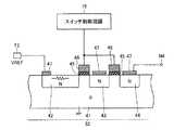
図9は、イメージセンサICの基本的な構成を示す概略図である。図9を参照して、イメージセンサIC111は受けた光を電気信号に変換する光電変換部112と、クランプ回路114とを備える。電位VREFは定電位であり、端子T102を介して外部から入力される。 FIG. 9 is a schematic diagram showing a basic configuration of the image sensor IC. Referring to FIG. 9, the image sensor IC 111 includes a
光電変換部112では、複数個の画素(図示せず)が直線上に配列される。各画素は受けた光の強度に応じて電気信号を生成する。各画素からの電気信号は光電変換部112の内部の増幅回路(図示せず)で増幅される。光電変換部112から出力される信号にはこの増幅回路の出力オフセット電圧が重畳されることにより、信号の基準となる電位が電位VREFからずれる。オフセット電圧はたとえば数10〜数100mV程度になる。 In the
クランプ回路114はノードNAの電位を電位VREFに設定するためのスイッチSW101と、光電変換部112の出力端子とノードNAとの間に接続されるコンデンサC100とを含む。スイッチSW101は、たとえばNチャネルMOSトランジスタやトランスミッションゲート等により構成される。 The
クランプ回路114では、まずスイッチSW101が導通することにより、ノードNAの電位が電位VREFになる。次にスイッチSW101が非導通状態になり、その後にコンデンサC100を介して光電変換部112から信号が送られる。光電変換部112から送られる信号に応じ、ノードNAにおける電位は電位VREFを基準に変化する。このように、コンデンサC100は光電変換部112から出力される信号の直流成分を遮断する役割を果たす。 In the
複数個のイメージセンサICの各々から出力される信号の基準電位レベルが揃っていないと、制御部(図示せず)で設定する信号のダイナミックレンジが小さくなってしまう。この場合、元の画像の階調を再現できなくなり、再現後の画像の解像度が低下するという問題が生じる。各ICに含まれるクランプ回路が信号の基準電位を電位VREFに固定することによって、このような問題を解決できる。 If the reference potential level of the signal output from each of the plurality of image sensor ICs is not uniform, the dynamic range of the signal set by the control unit (not shown) is reduced. In this case, there is a problem that the gradation of the original image cannot be reproduced and the resolution of the image after reproduction is lowered. Such a problem can be solved by the clamp circuit included in each IC fixing the reference potential of the signal to the potential VREF.
なお、クランプ回路114と端子T101との間には差動増幅回路A102が設けられる。差動増幅回路A102の非反転入力端子がノードNAに接続され、反転入力端子および出力端子が端子T101に接続されることで差動増幅回路A102はインピーダンス変換を行なう。また、ダイオードD101,D102は出力保護回路として機能し、ダイオードD103,D104は入力保護回路として機能する。 A differential amplifier circuit A102 is provided between the
従来、イメージセンサIC111を改良した様々なイメージセンサICが提案されている。たとえば特開2002−101264号公報(特許文献1)では、基準電位入力端子と信号出力端子との間に抵抗を設けることによって、クランプ容量の両端の電位差変動を抑えるイメージセンサIC(イメージセンサチップ)が開示される。 Conventionally, various image sensor ICs in which the
図10は、特開2002−101264号公報(特許文献1)に開示されるイメージセンサICの構成を概略的に示す図である。図10を参照して、イメージセンサIC111Aは端子T102とクランプ回路114との間に接続される抵抗R100をさらに備える点で図9に示すイメージセンサIC111と異なるが、他の部分の構成は同様であるので以後の説明は繰り返さない。 FIG. 10 is a diagram schematically showing a configuration of an image sensor IC disclosed in Japanese Patent Laid-Open No. 2002-101264 (Patent Document 1). Referring to FIG. 10, image sensor IC 111A is different from image sensor IC 111 shown in FIG. 9 in that it further includes a resistor R100 connected between terminal T102 and
イメージセンサIC111AではコンデンサC100と抵抗R100とによってハイパスフィルタが構成される。仮に光電変換部112とクランプ回路114との間にランダムノイズが生じたとしても、このハイパスフィルタがノイズを除去することにより、コンデンサC100の両端の電位差変動が抑えられる。よって、イメージセンサICごとにクランプレベルの変動を抑えることができ、高品質な画像信号を得ることが可能になる。
多くの画像入力機器においてイメージセンサ装置は可動であり、固定された回路基板とフレキシブルケーブルにより接続される。フレキシブルケーブルはアンテナ作用を有し、仮に画像入力機器の内部でノイズが生じると、そのノイズを受信する可能性がある。 In many image input devices, the image sensor device is movable and is connected to a fixed circuit board by a flexible cable. The flexible cable has an antenna function, and if noise occurs inside the image input device, there is a possibility of receiving the noise.
半導体装置において端子に接続される回路は、端子を介して外部と直接接続されるため、ノイズの影響を受けやすい。ノイズの中でもトランジスタを破壊するレベルのものは、サージと呼ばれる。このサージにより、MOSトランジスタのゲート絶縁膜の破壊などが生じる。したがって、MOSトランジスタにはサージに対する必要な程度の耐圧(静電耐圧)が要求される。 Since a circuit connected to a terminal in a semiconductor device is directly connected to the outside through the terminal, it is easily affected by noise. A noise level that destroys a transistor is called a surge. This surge causes destruction of the gate insulating film of the MOS transistor. Therefore, the MOS transistor is required to have a required withstand voltage (electrostatic withstand voltage) against a surge.
画像入力機器の動作が高速化されるにつれ、画像入力機器内部の電子部品からノイズが生じる可能性が高くなり、フレキシブルケーブルがノイズを受信する可能性が高くなっている。イメージセンサIC111の場合、端子T101,T102はこのフレキシブルケーブルに接続される。各端子にサージ保護のためのダイオードD101〜D104が設けられていても、端子に接続される金属配線を介し、内部回路にサージの影響が及ぶ可能性がある。 As the operation of the image input device is accelerated, there is a higher possibility that noise will be generated from the electronic components inside the image input device, and the possibility that the flexible cable will receive the noise is increased. In the case of the image sensor IC 111, the terminals T101 and T102 are connected to this flexible cable. Even if the diodes D101 to D104 for surge protection are provided at each terminal, there is a possibility that the internal circuit is affected by a surge through the metal wiring connected to the terminal.
特に入力端子である端子T102から入力されるサージの影響が大きいので、イメージセンサIC111ではスイッチSW101をサージから保護する必要がある。スイッチSW101のサイズを大きくすることによりスイッチSW101の静電耐圧を高くできる。具体的にはスイッチSW101を構成するMOSトランジスタのゲート幅を大きくすればよい。 In particular, since the influence of a surge input from the terminal T102 which is an input terminal is large, the image sensor IC 111 needs to protect the switch SW101 from the surge. The electrostatic withstand voltage of the switch SW101 can be increased by increasing the size of the switch SW101. Specifically, the gate width of the MOS transistor constituting the switch SW101 may be increased.
しかしながらスイッチSW101のサイズが大きくなると、スイッチSW101に入力される制御電位に応じて出力側(ノードNA側)の電位が変化する。ノードNAの電位の変動幅を以後「フィードスルー」(feed through)と称する。以下、スイッチSW101のサイズとフィードスルーとの関係について説明する。 However, when the size of the switch SW101 increases, the potential on the output side (node NA side) changes according to the control potential input to the switch SW101. The fluctuation range of the potential of the node NA is hereinafter referred to as “feed through”. Hereinafter, the relationship between the size of the switch SW101 and the feedthrough will be described.
図11は、図9に示すスイッチSW101の構成を示す図である。図11を参照して、スイッチSW101はNチャネルMOSトランジスタ121およびPチャネルMOSトランジスタ122を含む。ノードNAにはNチャネルMOSトランジスタ121の一方端と、PチャネルMOSトランジスタ122の一方端とが共通に接続される。端子T102にはNチャネルMOSトランジスタ121の他方端と、PチャネルMOSトランジスタ122の他方端とが共通に接続される。 FIG. 11 is a diagram showing the configuration of the switch SW101 shown in FIG. Referring to FIG. 11, switch SW101 includes an N
スイッチSW101の導通時、NチャネルMOSトランジスタ121のゲート電位は、たとえば3.3Vに設定され、PチャネルMOSトランジスタ122のゲート電位は0Vに設定される。一方、スイッチSW101の非導通時には、NチャネルMOSトランジスタ121のゲート電位は0Vに設定され、PチャネルMOSトランジスタ122のゲート電位は3.3Vに設定される。 When switch SW101 is turned on, the gate potential of N
NチャネルMOSトランジスタ121のノードNA側の一方端(ドレインまたはソース)とゲートとの間には寄生容量C101が存在する。また、PチャネルMOSトランジスタ122のノードNA側の一方端とゲートとの間には寄生容量C102が存在する。寄生容量C101,C102はMOSトランジスタのゲート電極と、ゲート酸化膜を介したゲート電極の下まで拡散するドレイン領域(またはソース領域)との間に生じる容量であり、一般的に「オーバラップ容量」と称される。 A parasitic capacitance C101 exists between one end (drain or source) of the N
オーバラップ容量はMOSトランジスタのゲート幅が大きいほど大きくなる。寄生容量C101,C102が大きいほど、スイッチSW101が導通状態から非導通状態に切り換った際にノードNAの電位が電位VREFから変化しやすくなる。つまりフィードスルーが大きくなる。なお、ノードNAの電位がどちらの方向に変動するかは寄生容量C101,C102に依存する。 The overlap capacitance increases as the gate width of the MOS transistor increases. As the parasitic capacitances C101 and C102 are larger, the potential of the node NA is more likely to change from the potential VREF when the switch SW101 is switched from the conductive state to the nonconductive state. That is, the feedthrough is increased. Note that the direction in which the potential of the node NA varies depends on the parasitic capacitances C101 and C102.
以上のようにイメージセンサIC111では静電耐圧を上げるためにスイッチSW101のサイズを大きくすると、フィードスルーが大きくなる。 As described above, in the
図10のイメージセンサIC111Aの場合、抵抗R100の抵抗値をある程度大きな値(たとえば数kΩ程度)に設定することで静電耐圧を高くできる。この場合、スイッチSW101のサイズを大きくしなくてもよいのでフィードスルーの発生を抑えることができる。 In the case of the
しかしスイッチSW101が導通すると、ノードNAの電位は(抵抗R100の抵抗値とスイッチSW101の抵抗値との和)×(コンデンサC100の容量値)により定まる時定数に従って変化する。抵抗R100の抵抗値が大きい程、ノードNAの電位が電位VREFに達するまでの時間が長くかかる。よって光電変換部112から信号を出力するタイミングを遅らせなければならない。 However, when the switch SW101 is turned on, the potential of the node NA changes according to a time constant determined by (the sum of the resistance value of the resistor R100 and the resistance value of the switch SW101) × (the capacitance value of the capacitor C100). The larger the resistance value of the resistor R100, the longer it takes for the potential of the node NA to reach the potential VREF. Therefore, the timing for outputting a signal from the
以上のようにイメージセンサIC111Aでは、静電耐圧を高くするほど動作速度が低下する可能性がある。 As described above, in the
このように、外部から受ける入力電位に基づいて処理を行なう従来の半導体装置の場合、動作に影響が生じることなく静電耐圧を向上させることが難しい。 Thus, in the case of a conventional semiconductor device that performs processing based on an input potential received from the outside, it is difficult to improve the electrostatic withstand voltage without affecting the operation.
本発明の目的は、外部から受ける入力電位に基づいて行なう処理に影響を与えることなく静電耐圧を向上させる半導体装置、そのような半導体装置を複数備えるモジュール、およびそのようなモジュールを備える電子機器を提供することである。 An object of the present invention is to provide a semiconductor device that improves electrostatic withstand voltage without affecting processing performed based on an input potential received from outside, a module including a plurality of such semiconductor devices, and an electronic apparatus including such a module. Is to provide.
本発明は要約すれば、半導体装置であって、入力電位を受ける入力端子と、第1の信号を受けてシフトさせ、入力電位を基準とする第2の信号を出力する変換回路とを備える。変換回路は、第1の信号が入力される第1のノードと第2の信号を出力する第2のノードとの間に接続されるコンデンサと、第2のノードと中間ノードとの間に設けられる第1のスイッチと、中間ノードと入力端子との間に設けられ、第1のスイッチとともに導通する第2のスイッチとを含む。 In summary, the present invention is a semiconductor device that includes an input terminal that receives an input potential, and a conversion circuit that receives and shifts a first signal and outputs a second signal based on the input potential. The conversion circuit is provided between the capacitor connected between the first node to which the first signal is input and the second node to output the second signal, and between the second node and the intermediate node. And a second switch that is provided between the intermediate node and the input terminal and is conductive with the first switch.
好ましくは、変換回路は、第2の信号の基準を入力電位に固定する。
好ましくは、半導体装置は、入射した光を電気信号に変換し、第1の信号を出力する光電変換部をさらに備える。Preferably, the conversion circuit fixes the reference of the second signal to the input potential.
Preferably, the semiconductor device further includes a photoelectric conversion unit that converts incident light into an electrical signal and outputs a first signal.
好ましくは、第1のスイッチは、他端部と中間ノードとの間に接続される第1のMOSトランジスタを有し、第2のスイッチは、入力端子と中間ノードとの間に接続され、バックゲートに定電位が与えられる第2のMOSトランジスタを有し、第2のMOSトランジスタのゲート幅は、第1のMOSトランジスタのゲート幅よりも大きい。 Preferably, the first switch has a first MOS transistor connected between the other end and the intermediate node, and the second switch is connected between the input terminal and the intermediate node, and the back There is a second MOS transistor to which a constant potential is applied to the gate, and the gate width of the second MOS transistor is larger than the gate width of the first MOS transistor.
より好ましくは、半導体装置は、第1および第2のMOSトランジスタを制御する制御回路をさらに備える。制御回路は、第1のMOSトランジスタを非導通状態に切換えた後に第2のMOSトランジスタを非導通状態に切換える。 More preferably, the semiconductor device further includes a control circuit that controls the first and second MOS transistors. The control circuit switches the second MOS transistor to the non-conductive state after switching the first MOS transistor to the non-conductive state.
さらに好ましくは、制御回路は、第2のMOSトランジスタを導通状態に設定した後に第1のMOSトランジスタを導通状態に設定する。 More preferably, the control circuit sets the first MOS transistor to the conductive state after setting the second MOS transistor to the conductive state.
さらに好ましくは、モジュールは上述のいずれかの半導体装置を複数備える。
さらに好ましくは、電子機器は、上述のモジュールを備える。More preferably, the module includes a plurality of any of the semiconductor devices described above.
More preferably, the electronic device includes the above-described module.
本発明の半導体装置によれば、信号の基準が外部から入力される入力電位になるように信号をシフトさせる変換回路と、その入力電位が与えられる入力端子との間に接続されるスイッチを備えることにより、変換回路の動作に影響を与えることなく静電耐圧を向上することができる。 According to the semiconductor device of the present invention, the conversion circuit that shifts the signal so that the reference of the signal becomes the input potential input from the outside, and the switch connected between the input terminal to which the input potential is applied are provided. Thus, the electrostatic withstand voltage can be improved without affecting the operation of the conversion circuit.
また、本発明のモジュールおよび電子機器によれば、上述の半導体装置を複数備えることにより、安定した動作を実現することができる。 In addition, according to the module and the electronic apparatus of the present invention, a stable operation can be realized by providing a plurality of the semiconductor devices described above.
以下において、本発明の実施の形態について図面を参照して詳しく説明する。なお、図中同一符号は同一または相当部分を示す。 Hereinafter, embodiments of the present invention will be described in detail with reference to the drawings. In the drawings, the same reference numerals indicate the same or corresponding parts.
図1は、本発明の電子機器の一例を示す図である。図1を参照して、本発明の電子機器の一例としてスキャナ100が示される。スキャナ100はイメージセンサヘッド1と、イメージセンサヘッド1に接続されるフレキシブルケーブル2と、フレキシブルケーブル2を介してイメージセンサヘッド1に接続される制御部3と、文字や画像などの情報が描かれた原稿を置くガラス4とを備える。 FIG. 1 is a diagram illustrating an example of an electronic apparatus of the present invention. Referring to FIG. 1, a
イメージセンサヘッド1は本発明のモジュールに相当する。イメージセンサヘッド1は可動であり、ガラス4を介して原稿から文字や画像を読み取り、制御部3に画像信号を送る。制御部3は画像信号に応じて画像を再現する。 The
スキャナ100はフラットベッドタイプのスキャナであるが、シートフィードスキャナであってもよい。シートフィードスキャナとはイメージセンサヘッドを固定し、一定速度で回転するローラーで原稿を送りながら、原稿上のイメージを読み取るスキャナである。また、本発明の電子機器は、スキャナに限定されず、たとえばファクシミリやコピー機等であってもよい。 The
図2は、図1のイメージセンサヘッド1の構成例を示す図である。図2を参照して、イメージセンサヘッド1は1次元に配置されたm個(mは自然数)のイメージセンサIC101〜10mを含む。イメージセンサIC101〜10mの各々は本発明の半導体装置に相当する。イメージセンサIC101〜10mは回路基板11に設けられた配線(図示せず)を介してフレキシブルケーブル2に接続され、電源電位や基準電位等が与えられる。 FIG. 2 is a diagram illustrating a configuration example of the
フレキシブルケーブル2を介してイメージセンサIC101〜10mに基準電位等を与える理由は以下のとおりである。まず、ノイズの影響を防ぐために回路基板11に電源回路や基準電位発生回路等を設けた場合には、回路基板11が大きくなるとともに重くなる。よって、回路基板11を動かそうとすれば消費電力が大きくなる。 The reason why a reference potential or the like is applied to the
また、別の理由として、イメージセンサIC101〜10mの各々に基準電位発生回路を内蔵させた場合には、特性のばらつきに起因して各ICから出力される信号の基準レベルが異なることが考えられるためである。 As another reason, when the reference potential generation circuit is incorporated in each of the
イメージセンサIC101〜10mは基準電位(入力電位)を受ける端子に印加されるサージから内部回路を保護する構成を有するため、フレキシブルケーブル2によるノイズの影響を受けにくくなる。よって、イメージセンサヘッド1およびスキャナ100の動作を安定させることができる。 Since the
図3は、図2のイメージセンサIC101の構成例を示す図である。図3を参照して、イメージセンサIC101は、光電変換部12、クランプ回路14、および端子T1、T2を備える。 FIG. 3 is a diagram illustrating a configuration example of the
光電変換部12は入射した光を電気信号に変換し、信号S1を出力する。光電変換部12は、n個(nは自然数)の画素P1〜Pn、および、画素P1〜Pnのそれぞれに対して設けられるスイッチRDSW1〜RDSWnを含む。スイッチRDSW1〜RDSWnを順次動作させることにより、画素P1〜Pnから電気信号が順次出力される。 The
光電変換部12は、さらに、スイッチSW0、差動増幅回路A1、および抵抗R1,R2を含む。スイッチSW0はノードN1と端子T2との間に接続される。端子T2は電位VREF(入力電位)を受ける。なお電位VREFは一定の電位である。 The
差動増幅回路A1の非反転入力端子はノードN1に接続され、反転入力端子は抵抗R1の一方端に接続される。抵抗R1の他方端はノードN2に接続される。抵抗R2は差動増幅回路A1の反転入力端子と端子T2との間に接続される。 The non-inverting input terminal of the differential amplifier circuit A1 is connected to the node N1, and the inverting input terminal is connected to one end of the resistor R1. The other end of resistor R1 is connected to node N2. The resistor R2 is connected between the inverting input terminal of the differential amplifier circuit A1 and the terminal T2.
画素から信号が出力される前にスイッチSW0が導通し、ノードN1の電位は電位VREFに設定される。差動増幅回路A1は画素から出力される信号を増幅し、ノードN2に信号S1を出力する。ただし、差動増幅回路A1から出力オフセット電圧が発生するので信号S1の基準電位は電位VREFからずれている。 Before the signal is output from the pixel, the switch SW0 is turned on, and the potential of the node N1 is set to the potential VREF. The differential amplifier circuit A1 amplifies the signal output from the pixel and outputs the signal S1 to the node N2. However, since an output offset voltage is generated from the differential amplifier circuit A1, the reference potential of the signal S1 is deviated from the potential VREF.
クランプ回路14は本発明における「変換回路」に相当する。クランプ回路14は信号S1をシフトさせ、電位VREFを基準とする信号S2を出力する。なお、クランプ回路14は信号S2の基準を電位VREFに固定する。 The
クランプ回路14は、コンデンサC1およびスイッチSW1,SW2を含む。コンデンサC1はノードN2に一方端が接続され、信号S2を出力するノードN3に他方端が接続される。スイッチSW1はノードN3とノードN4(中間ノード)との間に接続される。スイッチSW2はノードN4と端子T2との間に接続される。
スイッチSW1,SW2の各々は、たとえばトランスミッションゲートにより構成される。なお、スイッチSW1,SW2の各々は、NチャネルMOSトランジスタやPチャネルMOSトランジスタにより構成されてもよい。あるいはスイッチSW1,SW2の各々は、バイポーラトランジスタにより構成されてもよい。 Each of switches SW1 and SW2 is constituted by a transmission gate, for example. Each of switches SW1 and SW2 may be configured by an N channel MOS transistor or a P channel MOS transistor. Alternatively, each of the switches SW1 and SW2 may be configured by a bipolar transistor.
スイッチSW2に含まれるMOSトランジスタのゲート幅を大きくすることにより端子T2の電位と接地電位(あるいは電源電位)との間の耐圧が向上する。これにより端子T2にサージが印加された場合にもスイッチSW1等が保護される。また、スイッチSW2に含まれるMOSトランジスタのゲート幅を大きくすることにより、スイッチSW1のサイズを大きくしなくてもよいので、スイッチSW1が導通状態から非導通状態に変化したときのノードN3での電位の変動を抑えることができる。 Increasing the gate width of the MOS transistor included in the switch SW2 improves the breakdown voltage between the potential of the terminal T2 and the ground potential (or power supply potential). This protects the switch SW1 and the like even when a surge is applied to the terminal T2. Further, since the size of the switch SW1 does not need to be increased by increasing the gate width of the MOS transistor included in the switch SW2, the potential at the node N3 when the switch SW1 changes from the conductive state to the nonconductive state. Fluctuations can be suppressed.
さらに、コンデンサC1の容量値およびスイッチSW1,SW2の抵抗値により定まる時定数が小さくなり、信号S1の出力を開始するタイミングを遅らせなくてもよくなるので、高速動作への対応が可能になる。 Furthermore, the time constant determined by the capacitance value of the capacitor C1 and the resistance values of the switches SW1 and SW2 is reduced, and it is not necessary to delay the timing for starting the output of the signal S1, so that it is possible to cope with high-speed operation.
なお、スイッチSW2の導通時の抵抗、すなわちMOSトランジスタのオン抵抗は通常のサージ保護抵抗の抵抗値(数kΩ)よりも低く設定される(たとえば数Ω程度)。 Note that the resistance when the switch SW2 is turned on, that is, the on-resistance of the MOS transistor is set lower than the resistance value (several kΩ) of a normal surge protection resistor (for example, about several Ω).
イメージセンサIC101は、さらに、スイッチSW0〜SW2,RDSW1〜RDSWnを制御するスイッチ制御回路15を備える。スイッチ制御回路15は外部から入力されるクロック信号CLKに応じ各スイッチの導通および非導通のタイミングを制御する。 The
スイッチSW2はスイッチSW1とともに導通する。スイッチSW1,SW2がともに導通するとノードN3の電位は電位VREFに変化する。次にスイッチSW1,SW2がともに非導通状態になりノードN3の電位が電位VREFに保たれた状態で差動増幅回路A1から信号S1が送られる。 The switch SW2 becomes conductive together with the switch SW1. When both switches SW1 and SW2 are turned on, the potential at node N3 changes to potential VREF. Next, a signal S1 is sent from the differential amplifier circuit A1 in a state where both the switches SW1 and SW2 are in a non-conductive state and the potential of the node N3 is kept at the potential VREF.
コンデンサC1は出力される信号の直流成分を遮断する役割を果たす。よって信号S1に応じ、信号S2の電位は電位VREFを基準として変化する。 The capacitor C1 serves to block the direct current component of the output signal. Therefore, in response to the signal S1, the potential of the signal S2 changes with the potential VREF as a reference.
イメージセンサIC101は、さらに、インピーダンス変換回路として機能する差動増幅回路A2を備える。差動増幅回路A2の非反転入力端子は信号S2を受け、反転入力端子および出力端子が端子T1に接続される。端子T1から外部に信号SOUTが出力される。 The
イメージセンサIC101は、さらに、保護素子として機能するダイオードD1〜D4を備える。ダイオードD1はノードN0(電源ノード)と端子T1との間に接続される。ダイオードD2は端子T1と接地ノードとの間に接続される。ダイオードD3はノードN0と端子T2との間に接続される。ダイオードD4は端子T2と接地ノードとの間に接続される。 The
なお、イメージセンサIC102〜10mの各々の構成はイメージセンサIC101の構成と同様であるので以後の説明は繰り返さない。 The configuration of each of
図4は、図3のスイッチSW1の構成例を示す図である。図4を参照して、スイッチSW1はNチャネルMOSトランジスタ21とPチャネルMOSトランジスタ22とインバータ23とを含む。NチャネルMOSトランジスタ21およびPチャネルMOSトランジスタ22はノードN3とノードN4との間に並列に接続される。NチャネルMOSトランジスタ21のゲートはノードN11に接続され、PチャネルMOSトランジスタ22のゲートはノードN12に接続される。インバータ23はノードN11に入力端子が接続され、ノードN12に出力端子が接続される。 FIG. 4 is a diagram illustrating a configuration example of the switch SW1 of FIG. Referring to FIG. 4, switch
スイッチSW1は、さらに、NチャネルMOSトランジスタ24とPチャネルMOSトランジスタ25とを含む。NチャネルMOSトランジスタ21とPチャネルMOSトランジスタ22との各々のゲート幅を小さくすることでフィードスルーの発生を抑えることができるが、さらにフィードスルーを抑えるため、NチャネルMOSトランジスタ24とPチャネルMOSトランジスタ25とが補助的に設けられる。
NチャネルMOSトランジスタ24の一方端はノードN3に接続され、他方端は開放され、ゲートはノードN12に接続される。NチャネルMOSトランジスタ24のサイズはNチャネルMOSトランジスタ21と同じである。 One end of N
PチャネルMOSトランジスタ25の一方端はノードN3に接続され、他方端は開放され、ゲートはノードN11に接続される。PチャネルMOSトランジスタ25のサイズはPチャネルMOSトランジスタ22と同じである。 One end of P-
以下、NチャネルMOSトランジスタ21,24を例にフィードスルーを抑える作用について説明するが、PチャネルMOSトランジスタ22,25についても同様の作用が生じる。 The operation of suppressing feedthrough will be described below by taking N
ノードN11の電位がたとえば3.3Vから0Vに変化すると、NチャネルMOSトランジスタ21の寄生容量(ノードN11とノードN3との間の容量)はノードN3の電位を電位VREFよりも低下させようとする。しかし、NチャネルMOSトランジスタ24のゲートの電位が0Vから3.3Vに変化するので、NチャネルMOSトランジスタ24の寄生容量(ノードN12とノードN3との間の容量)はノードN3の電位を電位VREFよりも上昇させようとする。各NチャネルMOSトランジスタの容量値が等しいため、これらの電位変化が相殺されることでノードN3での電位は電位VREFに保たれる。 When the potential of node N11 changes from 3.3V to 0V, for example, the parasitic capacitance of N channel MOS transistor 21 (capacitance between node N11 and node N3) attempts to lower the potential of node N3 below potential VREF. . However, since the gate potential of N-
図5は、図3のスイッチSW2の構成例を示す図である。図5を参照して、スイッチSW2は、PチャネルMOSトランジスタ31とNチャネルMOSトランジスタ32とインバータ33とを含む。 FIG. 5 is a diagram illustrating a configuration example of the switch SW2 of FIG. Referring to FIG. 5, switch SW <b> 2 includes a P
PチャネルMOSトランジスタ31はノードN4と端子T2との間に接続される。PチャネルMOSトランジスタ31のゲートはノードN21に接続され、バックゲートは電源電位(定電位)を与えるノードN0に接続される。 P-
NチャネルMOSトランジスタ32はノードN4と端子T2との間に接続される。NチャネルMOSトランジスタ32のゲートはノードN22に接続され、バックゲートは接地電位(定電位)を与える接地ノードに接続される。 N-
インバータ33の入力端子はノードN21に接続され、インバータ33の出力端子はノードN22に接続される。 The input terminal of
PチャネルMOSトランジスタ31のゲート幅はPチャネルMOSトランジスタ22のゲート幅よりも大きい。また、NチャネルMOSトランジスタ32のゲート幅はNチャネルMOSトランジスタ21のゲート幅よりも大きい。たとえばPチャネルMOSトランジスタ31,22のゲート幅はそれぞれ約170μm、約9μmである。また、NチャネルMOSトランジスタ32,21のゲート幅はそれぞれ約53μm、約2.5μmである。このように、スイッチSW2に含まれるMOSトランジスタのゲート幅を大きくすることによって静電耐圧を向上することができる。 The gate width of P
図6は、図5のNチャネルMOSトランジスタ32の断面を模式的に示す図である。図6を参照して、NチャネルMOSトランジスタ32はP型の半導体基板41に形成される。半導体基板41にはN型の拡散層42〜44が形成される。半導体基板41は接地電位に設定され、NチャネルMOSトランジスタ32のバックゲートとなる。また、拡散層42は他の拡散層よりも広く形成される。 FIG. 6 is a diagram schematically showing a cross section of the N-
拡散層42と拡散層43との間、および拡散層43と拡散層44との間はチャネル領域である。各チャネル領域上にゲート酸化膜45が形成され、ゲート酸化膜45上にはスイッチ制御回路15に接続されるゲート電極46が形成される。 Between the
拡散層42〜44の上部にはシリサイド47が形成される。拡散層42上のシリサイド47はゲート電極から離れた位置に設けられ、金属配線を介して端子T2に接続される。拡散層44上のシリサイド47はノードN4に接続される。なお、拡散層43上のシリサイド47はフローティング状態になっている。 A
端子T2にサージが印加された場合、拡散層42が抵抗の役割を果たしているのでゲート酸化膜45の破壊を防ぐことができる。また、拡散層42と半導体基板41とはダイオードを構成する。接地電位に対する端子T2の電圧がある過電圧レベル(たとえば200〜400V)を超えると、端子T2から拡散層42と半導体基板41とを通り、接地ノードに向けてサージ電流が流れる。ゲート電極46の幅を大きくすることにより、ダイオードに流れるサージ電流を大きくすることができる。 When a surge is applied to the terminal T2, the
図7は、図5のPチャネルMOSトランジスタ31の断面を模式的に示す図である。図7を参照して、PチャネルMOSトランジスタ31は、半導体基板41にN型の拡散層51が形成され、拡散層51内にP型の拡散層42〜44が形成される点で図6のNチャネルMOSトランジスタ32と異なるが他の点は同様であるので以後の説明は繰り返さない。拡散層51はPチャネルMOSトランジスタ31のバックゲートとなり、ノードN0から電源電位が与えられる。拡散層51と拡散層42とはダイオードを構成する。端子T2に正方向のサージが印加された場合、端子T2から拡散層42および拡散層51を通り、ノードN0に向けてサージ電流が流れる。 FIG. 7 is a diagram schematically showing a cross section of the P-
図8は、図2のイメージセンサIC101の動作を説明するタイミングチャートである。図8を参照して、まず時刻t1においてクロック信号CLKの立ち上がりに応じ、スイッチSW0およびスイッチSW2がともに導通状態(ON状態)に変化する。よってノードN1,N4の電位が電位VREFに変化する。図8において電位VREFは1Vである。 FIG. 8 is a timing chart for explaining the operation of the
電位VA,VBは図3の信号S1,S2の電位をそれぞれ示す。電位VAは時刻t1以前は不定であるが、時刻t1において1.05Vに変化する。電位VAと電位VREFとの電位差(0.05V)は差動増幅回路A1から生じる出力オフセット電圧である。 The potentials VA and VB indicate the potentials of the signals S1 and S2 in FIG. The potential VA is indefinite before time t1, but changes to 1.05 V at time t1. A potential difference (0.05 V) between the potential VA and the potential VREF is an output offset voltage generated from the differential amplifier circuit A1.
時刻t2におけるクロック信号の立ち上がりに応じ、スイッチSW1が導通状態に変化する。ノードN3の電位は時刻t2以前は不定であるが、時刻t2において電位VREF(1V)に変化する。 In response to the rise of the clock signal at time t2, the switch SW1 changes to a conductive state. The potential of the node N3 is indefinite before time t2, but changes to the potential VREF (1 V) at time t2.
このようにスイッチ制御回路15はスイッチSW2(PチャネルMOSトランジスタ31、NチャネルMOSトランジスタ32)を導通状態に設定した後にスイッチSW1(PチャネルMOSトランジスタ22、NチャネルMOSトランジスタ21)を導通状態に設定する。これによりノードN4の電位が電位VREFに達した状態でスイッチSW1が導通状態に設定されるので、ノードN3の電位が電位VREFに達する時間を短くすることができる。 Thus, the
続いて時刻t3におけるクロック信号CLKの立ち上がりに応じ、スイッチSW1が非導通状態(OFF状態)に変化する。ただし電位VBは1Vのまま変化しない。さらに時刻t4におけるクロック信号CLKの立ち上がりに応じ、スイッチSW0,SW2がともに非導通状態に変化する。 Subsequently, in response to the rise of the clock signal CLK at time t3, the switch SW1 changes to a non-conduction state (OFF state). However, the potential VB remains 1V and does not change. Furthermore, both the switches SW0 and SW2 change to the non-conductive state in response to the rising of the clock signal CLK at time t4.
このようにスイッチ制御回路15はスイッチSW1を非導通状態に切換えた後にスイッチSW2を非導通状態に切換える。これによって、スイッチSW2が非導通状態に変化しても電位VBはスイッチSW2の影響を受けなくなる。 As described above, the
さらに時刻t5におけるクロック信号CLKの立ち上がりに応じてスイッチRDSW1が導通状態に変化すると、画素P1から出力された信号が差動増幅回路A1により増幅される。電位VAは1.05Vを基準として変化するのに対し、電位VBは1.0Vを基準として変化する。続いて時刻t6におけるクロック信号CLKの立ち上がりに応じてスイッチRDSW2が導通状態に変化すると、時刻t5〜時刻t6の期間と同様に電位VA,VBが変化する。電位VBは1.0Vすなわち電位VREFを基準に変化する。このようにクランプ回路14は信号S1をシフトさせ、電位VREFを基準とする信号S2を出力する。また、クランプ回路14は信号S2の基準を電位VREFに固定する。 Further, when the switch RDSW1 changes to the conductive state in response to the rise of the clock signal CLK at time t5, the signal output from the pixel P1 is amplified by the differential amplifier circuit A1. The potential VA changes with 1.05V as a reference, whereas the potential VB changes with 1.0V as a reference. Subsequently, when the switch RDSW2 changes to a conductive state in response to the rise of the clock signal CLK at time t6, the potentials VA and VB change as in the period from time t5 to time t6. The potential VB changes with respect to 1.0 V, that is, the potential VREF. Thus, the
以上のように本発明の実施の形態によれば、外部から受ける入力電位に基づいて処理を行なう半導体装置において、入力電位を受ける入力端子と第1のスイッチとの間に第2のスイッチを設け、第2のスイッチのサイズを大きくすることによって、第2のスイッチがサージを吸収するので静電耐圧を向上させることができる。 As described above, according to the embodiment of the present invention, in the semiconductor device that performs processing based on the input potential received from the outside, the second switch is provided between the input terminal that receives the input potential and the first switch. By increasing the size of the second switch, the second switch absorbs the surge, so that the electrostatic withstand voltage can be improved.
また、本発明の実施の形態によれば、第2のスイッチの抵抗値をサージ吸収用の抵抗よりも低くすることによって、クランプ動作への影響を防ぐことができる。 Further, according to the embodiment of the present invention, it is possible to prevent the influence on the clamping operation by making the resistance value of the second switch lower than the resistance for surge absorption.
また、本発明の実施の形態によれば、第2のスイッチに用いられるMOSトランジスタのゲート幅を第1のスイッチに用いられるMOSトランジスタのゲート幅よりも大きくすることによってフィードスルーの発生を抑えることができる。 Further, according to the embodiment of the present invention, the occurrence of feedthrough is suppressed by making the gate width of the MOS transistor used for the second switch larger than the gate width of the MOS transistor used for the first switch. Can do.
また、本発明の実施の形態によれば、画像入力装置に用いられるイメージセンサヘッドが上述の半導体装置を複数備えることにより、画像入力装置の内部でノイズが発生しても安定した動作を行なうことが可能になる。 According to the embodiment of the present invention, the image sensor head used in the image input device includes a plurality of the above-described semiconductor devices, so that stable operation can be performed even if noise is generated inside the image input device. Is possible.
なお、本実施の形態では半導体装置の一例としてイメージセンサICを示したが、本発明の半導体装置は、信号をシフトさせ、外部から受ける入力電位を基準とする信号を出力する回路を備える半導体装置に広く適用が可能である。 Note that although an image sensor IC is shown as an example of a semiconductor device in this embodiment, the semiconductor device of the present invention includes a circuit that shifts a signal and outputs a signal based on an input potential received from the outside. Widely applicable to.
今回開示された実施の形態はすべての点で例示であって制限的なものではないと考えられるべきである。本発明の範囲は上記した説明ではなくて特許請求の範囲によって示され、特許請求の範囲と均等の意味および範囲内でのすべての変更が含まれることが意図される。 The embodiment disclosed this time should be considered as illustrative in all points and not restrictive. The scope of the present invention is defined by the terms of the claims, rather than the description above, and is intended to include any modifications within the scope and meaning equivalent to the terms of the claims.
1 イメージセンサヘッド、2 フレキシブルケーブル、3 制御部、4 ガラス、11 回路基板、12,112 光電変換部、14,114 クランプ回路、15 スイッチ制御回路、21,24,32,121 NチャネルMOSトランジスタ、22,25,31,122 PチャネルMOSトランジスタ、23,33 インバータ、41 半導体基板、42〜44,51 拡散層、45 ゲート酸化膜、46 ゲート電極、47 シリサイド、100 スキャナ、101〜10m,111,111A イメージセンサIC、A1,A2,A102 差動増幅回路、C1,C100 コンデンサ、C101,C102 寄生容量、D1〜D4,D101〜D104 ダイオード、N0〜N4,N11,N12,N21,N22,NA ノード、P1〜Pn 画素、T1,T2,T101,T102 端子、R1,R2,R100 抵抗、RDSW1〜RDSWn,SW0〜SW2,SW101 スイッチ。 DESCRIPTION OF
Claims (8)
Translated fromJapanese第1の信号を受けてシフトさせ、前記入力電位を基準とする第2の信号を出力する変換回路とを備え、
前記変換回路は、
前記第1の信号が入力される第1のノードと前記第2の信号を出力する第2のノードとの間に接続されるコンデンサと、
前記第2のノードと中間ノードとの間に設けられる第1のスイッチと、
前記中間ノードと前記入力端子との間に設けられ、前記第1のスイッチとともに導通する第2のスイッチとを含む、半導体装置。An input terminal for receiving an input potential;
A conversion circuit that receives and shifts the first signal and outputs a second signal based on the input potential,
The conversion circuit includes:
A capacitor connected between a first node to which the first signal is input and a second node that outputs the second signal;
A first switch provided between the second node and the intermediate node;
A semiconductor device comprising: a second switch provided between the intermediate node and the input terminal and conducting together with the first switch.
前記他端部と前記中間ノードとの間に接続される第1のMOSトランジスタを有し、
前記第2のスイッチは、
前記入力端子と前記中間ノードとの間に接続され、バックゲートに定電位が与えられる第2のMOSトランジスタを有し、
前記第2のMOSトランジスタのゲート幅は、前記第1のMOSトランジスタのゲート幅よりも大きい、請求項1に記載の半導体装置。The first switch is
A first MOS transistor connected between the other end and the intermediate node;
The second switch is
A second MOS transistor connected between the input terminal and the intermediate node and having a constant potential applied to a back gate;
The semiconductor device according to claim 1, wherein a gate width of the second MOS transistor is larger than a gate width of the first MOS transistor.
前記第1および第2のMOSトランジスタを制御する制御回路をさらに備え、
前記制御回路は、前記第1のMOSトランジスタを非導通状態に切換えた後に前記第2のMOSトランジスタを非導通状態に切換える、請求項4に記載の半導体装置。The semiconductor device includes:
A control circuit for controlling the first and second MOS transistors;
5. The semiconductor device according to claim 4, wherein the control circuit switches the second MOS transistor to a non-conductive state after switching the first MOS transistor to a non-conductive state.
Priority Applications (6)
| Application Number | Priority Date | Filing Date | Title |
|---|---|---|---|
| JP2005213303AJP2007035726A (en) | 2005-07-22 | 2005-07-22 | Semiconductor device, module and electronic device |
| PCT/JP2006/314062WO2007010854A1 (en) | 2005-07-22 | 2006-07-14 | Semiconductor device, module and electronic device |
| CNA2006800266920ACN101228778A (en) | 2005-07-22 | 2006-07-14 | Semiconductor device, module, and electronic apparatus |
| US11/996,209US7608810B2 (en) | 2005-07-22 | 2006-07-14 | Semiconductor device, module, and electronic device including a conversion circuit having a second switch rendered conductive together with a first switch |
| KR1020087003544AKR20080030096A (en) | 2005-07-22 | 2006-07-14 | Semiconductor devices, modules and electronics |
| TW095126731ATW200709670A (en) | 2005-07-22 | 2006-07-21 | Semiconductor device, module and electronic device |
Applications Claiming Priority (1)
| Application Number | Priority Date | Filing Date | Title |
|---|---|---|---|
| JP2005213303AJP2007035726A (en) | 2005-07-22 | 2005-07-22 | Semiconductor device, module and electronic device |
Publications (1)
| Publication Number | Publication Date |
|---|---|
| JP2007035726Atrue JP2007035726A (en) | 2007-02-08 |
Family
ID=37668735
Family Applications (1)
| Application Number | Title | Priority Date | Filing Date |
|---|---|---|---|
| JP2005213303APendingJP2007035726A (en) | 2005-07-22 | 2005-07-22 | Semiconductor device, module and electronic device |
Country Status (6)
| Country | Link |
|---|---|
| US (1) | US7608810B2 (en) |
| JP (1) | JP2007035726A (en) |
| KR (1) | KR20080030096A (en) |
| CN (1) | CN101228778A (en) |
| TW (1) | TW200709670A (en) |
| WO (1) | WO2007010854A1 (en) |
Families Citing this family (39)
| Publication number | Priority date | Publication date | Assignee | Title |
|---|---|---|---|---|
| US8262900B2 (en) | 2006-12-14 | 2012-09-11 | Life Technologies Corporation | Methods and apparatus for measuring analytes using large scale FET arrays |
| CA2672315A1 (en) | 2006-12-14 | 2008-06-26 | Ion Torrent Systems Incorporated | Methods and apparatus for measuring analytes using large scale fet arrays |
| US11339430B2 (en) | 2007-07-10 | 2022-05-24 | Life Technologies Corporation | Methods and apparatus for measuring analytes using large scale FET arrays |
| US8349167B2 (en) | 2006-12-14 | 2013-01-08 | Life Technologies Corporation | Methods and apparatus for detecting molecular interactions using FET arrays |
| CN102203282B (en) | 2008-06-25 | 2014-04-30 | 生命技术公司 | Methods and apparatus for measuring analytes using large scale FET arrays |
| US20100137143A1 (en) | 2008-10-22 | 2010-06-03 | Ion Torrent Systems Incorporated | Methods and apparatus for measuring analytes |
| US20100301398A1 (en) | 2009-05-29 | 2010-12-02 | Ion Torrent Systems Incorporated | Methods and apparatus for measuring analytes |
| US8673627B2 (en) | 2009-05-29 | 2014-03-18 | Life Technologies Corporation | Apparatus and methods for performing electrochemical reactions |
| US8776573B2 (en) | 2009-05-29 | 2014-07-15 | Life Technologies Corporation | Methods and apparatus for measuring analytes |
| US20120261274A1 (en) | 2009-05-29 | 2012-10-18 | Life Technologies Corporation | Methods and apparatus for measuring analytes |
| EP2357468B1 (en)* | 2010-01-21 | 2017-09-20 | Nxp B.V. | Sensor and measurement method |
| WO2012003363A1 (en) | 2010-06-30 | 2012-01-05 | Life Technologies Corporation | Ion-sensing charge-accumulation circuits and methods |
| TWI539172B (en) | 2010-06-30 | 2016-06-21 | 生命技術公司 | Methods and apparatus for testing isfet arrays |
| JP2013540259A (en) | 2010-06-30 | 2013-10-31 | ライフ テクノロジーズ コーポレーション | Array column integrator |
| US11307166B2 (en) | 2010-07-01 | 2022-04-19 | Life Technologies Corporation | Column ADC |
| EP2589065B1 (en) | 2010-07-03 | 2015-08-19 | Life Technologies Corporation | Chemically sensitive sensor with lightly doped drains |
| WO2012036679A1 (en) | 2010-09-15 | 2012-03-22 | Life Technologies Corporation | Methods and apparatus for measuring analytes |
| US8796036B2 (en) | 2010-09-24 | 2014-08-05 | Life Technologies Corporation | Method and system for delta double sampling |
| US9970984B2 (en) | 2011-12-01 | 2018-05-15 | Life Technologies Corporation | Method and apparatus for identifying defects in a chemical sensor array |
| US8747748B2 (en) | 2012-01-19 | 2014-06-10 | Life Technologies Corporation | Chemical sensor with conductive cup-shaped sensor surface |
| US8821798B2 (en) | 2012-01-19 | 2014-09-02 | Life Technologies Corporation | Titanium nitride as sensing layer for microwell structure |
| US8786331B2 (en) | 2012-05-29 | 2014-07-22 | Life Technologies Corporation | System for reducing noise in a chemical sensor array |
| US9080968B2 (en) | 2013-01-04 | 2015-07-14 | Life Technologies Corporation | Methods and systems for point of use removal of sacrificial material |
| US9841398B2 (en) | 2013-01-08 | 2017-12-12 | Life Technologies Corporation | Methods for manufacturing well structures for low-noise chemical sensors |
| US8962366B2 (en) | 2013-01-28 | 2015-02-24 | Life Technologies Corporation | Self-aligned well structures for low-noise chemical sensors |
| US8841217B1 (en) | 2013-03-13 | 2014-09-23 | Life Technologies Corporation | Chemical sensor with protruded sensor surface |
| US8963216B2 (en) | 2013-03-13 | 2015-02-24 | Life Technologies Corporation | Chemical sensor with sidewall spacer sensor surface |
| EP2972279B1 (en) | 2013-03-15 | 2021-10-06 | Life Technologies Corporation | Chemical sensors with consistent sensor surface areas |
| US9835585B2 (en) | 2013-03-15 | 2017-12-05 | Life Technologies Corporation | Chemical sensor with protruded sensor surface |
| EP2972280B1 (en) | 2013-03-15 | 2021-09-29 | Life Technologies Corporation | Chemical sensor with consistent sensor surface areas |
| US9116117B2 (en) | 2013-03-15 | 2015-08-25 | Life Technologies Corporation | Chemical sensor with sidewall sensor surface |
| JP6671274B2 (en) | 2013-03-15 | 2020-03-25 | ライフ テクノロジーズ コーポレーション | Chemical device with thin conductive element |
| US20140336063A1 (en) | 2013-05-09 | 2014-11-13 | Life Technologies Corporation | Windowed Sequencing |
| US10458942B2 (en) | 2013-06-10 | 2019-10-29 | Life Technologies Corporation | Chemical sensor array having multiple sensors per well |
| JP6308925B2 (en)* | 2014-09-29 | 2018-04-11 | ルネサスエレクトロニクス株式会社 | Semiconductor device |
| US10077472B2 (en) | 2014-12-18 | 2018-09-18 | Life Technologies Corporation | High data rate integrated circuit with power management |
| KR102593647B1 (en) | 2014-12-18 | 2023-10-26 | 라이프 테크놀로지스 코포레이션 | High data rate integrated circuit with transmitter configuration |
| CN107407656B (en) | 2014-12-18 | 2020-04-07 | 生命科技公司 | Method and apparatus for measuring analytes using large scale FET arrays |
| CN119561529B (en)* | 2025-01-24 | 2025-05-13 | 合肥市山海半导体技术有限公司 | A CMOS switch circuit |
Citations (2)
| Publication number | Priority date | Publication date | Assignee | Title |
|---|---|---|---|---|
| JPH05210976A (en)* | 1991-11-08 | 1993-08-20 | Hitachi Ltd | Semiconductor integrated circuit |
| JP2005012752A (en)* | 2003-02-26 | 2005-01-13 | Seiko Instruments Inc | Signal processing circuit, image sensor IC, and signal processing method |
Family Cites Families (3)
| Publication number | Priority date | Publication date | Assignee | Title |
|---|---|---|---|---|
| KR100254134B1 (en)* | 1991-11-08 | 2000-04-15 | 나시모토 류우조오 | Semiconductor integrated circuit having current reduction circuit in the standby state |
| JP2002101264A (en) | 2000-09-25 | 2002-04-05 | Canon Inc | Image sensor chip and image reading device using the same |
| US6952226B2 (en)* | 2000-12-22 | 2005-10-04 | Texas Instruments Incorporated | Stray-insensitive, leakage-independent image sensing with reduced sensitivity to device mismatch and parasitic routing capacitance |
- 2005
- 2005-07-22JPJP2005213303Apatent/JP2007035726A/enactivePending
- 2006
- 2006-07-14WOPCT/JP2006/314062patent/WO2007010854A1/enactiveApplication Filing
- 2006-07-14KRKR1020087003544Apatent/KR20080030096A/ennot_activeCeased
- 2006-07-14USUS11/996,209patent/US7608810B2/ennot_activeExpired - Fee Related
- 2006-07-14CNCNA2006800266920Apatent/CN101228778A/enactivePending
- 2006-07-21TWTW095126731Apatent/TW200709670A/enunknown
Patent Citations (2)
| Publication number | Priority date | Publication date | Assignee | Title |
|---|---|---|---|---|
| JPH05210976A (en)* | 1991-11-08 | 1993-08-20 | Hitachi Ltd | Semiconductor integrated circuit |
| JP2005012752A (en)* | 2003-02-26 | 2005-01-13 | Seiko Instruments Inc | Signal processing circuit, image sensor IC, and signal processing method |
Also Published As
| Publication number | Publication date |
|---|---|
| US7608810B2 (en) | 2009-10-27 |
| KR20080030096A (en) | 2008-04-03 |
| TW200709670A (en) | 2007-03-01 |
| US20090032682A1 (en) | 2009-02-05 |
| WO2007010854A1 (en) | 2007-01-25 |
| CN101228778A (en) | 2008-07-23 |
Similar Documents
| Publication | Publication Date | Title |
|---|---|---|
| JP2007035726A (en) | Semiconductor device, module and electronic device | |
| US8749276B2 (en) | Signal buffer circuit, sensor control board, image scanner, and image forming apparatus | |
| JP2008271159A (en) | Solid-state imaging device | |
| JP4854410B2 (en) | Semiconductor device | |
| JP2004241491A (en) | Solid-state imaging device | |
| JP2011250554A (en) | Power circuit, integrated circuit device, solid state image pickup device, and electronic apparatus | |
| TW201316764A (en) | Power stabilizing circuit | |
| JP4935227B2 (en) | Temperature detection circuit, operation method thereof, and semiconductor device | |
| US20060001752A1 (en) | CMOS image sensor for reducing kTC noise, reset transistor control circuit used in the image sensor and voltage switch circuit used in the control circuit | |
| EP0013099B1 (en) | Semiconductor integrated circuit device including a reference voltage generator feeding a plurality of loads | |
| JP4318511B2 (en) | Booster circuit | |
| KR0163728B1 (en) | Constant voltage generating circuit comprising bi-mos | |
| US5773872A (en) | Semiconductor device having an integrated differential circuit with an improved common-mode rejection ratio (CMRR) | |
| US6291810B1 (en) | Image sensor | |
| JP5082872B2 (en) | Soft start circuit | |
| CN114296500B (en) | Multiplexing circuit for multiple reference voltages | |
| US7605853B2 (en) | Solid-state image sensing device and camera | |
| GB2260661A (en) | Power supply circuit for semiconductor memory device | |
| JPH09321595A (en) | Switching circuit and ad converter circuit using it | |
| JP2010130555A (en) | Voltage follower circuit | |
| JP2006148320A (en) | Switched capacitor filter | |
| JP4712497B2 (en) | Filter circuit, and image sensor, image sensor module, and image reading apparatus using the same | |
| JP2009105246A (en) | Photoelectric conversion element, solid-state imaging device, and electronic device | |
| JP4427566B2 (en) | Semiconductor device | |
| JP2008219282A (en) | Photoelectric conversion device |
Legal Events
| Date | Code | Title | Description |
|---|---|---|---|
| A621 | Written request for application examination | Free format text:JAPANESE INTERMEDIATE CODE: A621 Effective date:20080714 | |
| A131 | Notification of reasons for refusal | Free format text:JAPANESE INTERMEDIATE CODE: A131 Effective date:20111129 | |
| A02 | Decision of refusal | Free format text:JAPANESE INTERMEDIATE CODE: A02 Effective date:20120321 |