JP2007035063A - Simd type processor - Google Patents
Simd type processorDownload PDFInfo
- Publication number
- JP2007035063A JP2007035063AJP2006259487AJP2006259487AJP2007035063AJP 2007035063 AJP2007035063 AJP 2007035063AJP 2006259487 AJP2006259487 AJP 2006259487AJP 2006259487 AJP2006259487 AJP 2006259487AJP 2007035063 AJP2007035063 AJP 2007035063A
- Authority
- JP
- Japan
- Prior art keywords
- data
- register
- processor
- processor element
- signal
- Prior art date
- Legal status (The legal status is an assumption and is not a legal conclusion. Google has not performed a legal analysis and makes no representation as to the accuracy of the status listed.)
- Granted
Links
Images


Landscapes
- Image Processing (AREA)
Abstract
Description
Translated fromJapaneseこの発明は、一つの演算命令により複数の画像データ等を並列処理するSIMD(Single Instruction Stream Multiple Data Stream)型プロセッサに関するものである。 The present invention relates to a single instruction stream multiple data stream (SIMD) type processor that processes a plurality of image data and the like in parallel by one arithmetic instruction.
近年、デジタル複写機やファクリミリ装置等において、画素数を増加させたり、或いはカラー対応にするなど画像の向上が図られている。そして、この画像の向上に伴い、処理すべきデータ数が増加している。ところで、複写機などにおけるデータ処理は全ての画素に対して同じ演算処理を施すことが多い。そこで、1つの命令で複数のデータに対して同時に同じ演算処理を行うSIMD型プロセッサが用いられるようになっている。ここで、演算処理は複数の演算器を並べることで実現できるが、演算の対象となるデータは演算速度に見合う速度でメモリ等をアクセスする必要があり、この速度に間に合わない場合はデータのアクセス速度でプロセッサの性能が決定してしまう。通常タイプのSISD(Single Instruction Single Data)型プロセッサでは、演算データはプロセッサのプログラムによりメモリから逐次アクセスするが、この場合にデータのアクセス速度はメモリのビット幅と転送時間で決定する。SIMD型プロセッサにおいてもこの方法を用いると演算は並列処理であるのに対して、データのアクセスは逐次処理となりSISD型プロセッサ程度に処理能力は低下してしまう。 In recent years, in digital copying machines, facsimile machines, and the like, improvement of images has been attempted by increasing the number of pixels or making it compatible with color. As the image is improved, the number of data to be processed has increased. By the way, data processing in a copying machine or the like often performs the same arithmetic processing on all pixels. Therefore, a SIMD type processor that performs the same arithmetic processing simultaneously on a plurality of data with one instruction is used. Here, arithmetic processing can be realized by arranging a plurality of arithmetic units, but it is necessary to access the memory etc. at a speed commensurate with the arithmetic speed for the data to be operated. Processor performance is determined by speed. In a normal type SIDS (Single Instruction Single Data) processor, operation data is sequentially accessed from a memory by a program of the processor. In this case, the data access speed is determined by the bit width of the memory and the transfer time. If this method is also used in the SIMD type processor, the computation is parallel processing, whereas the data access is sequential processing, and the processing capability is reduced to the same level as the SISD type processor.
このため、SIMD型プロセッサでは、演算対象データのアクセスはプロセッサの命令では行わず、外部のメモリデータ転送装置からプロセッサ内部の入出力用のレジスタに直接アクセスするように構成している。即ち、プロセッサでの演算実行と同時に、外部に備えられたメモリデータ転送装置が次に演算処理されるデータを入力用レジスタへ転送したり、演算処理されたデータを出力レジスタからメモリデータ転送装置を介してメモリへ転送することで、データ処理の高速化を図っている。 For this reason, the SIMD type processor is configured such that the operation target data is not accessed by a processor instruction, but an input / output register inside the processor is directly accessed from an external memory data transfer device. In other words, simultaneously with the execution of the operation by the processor, the memory data transfer device provided outside transfers the data to be processed next to the input register, or the calculated data is transferred from the output register to the memory data transfer device. The data processing speed is increased by transferring the data to the memory.
プロセッサと外部メモリデータ転送装置での処理フローは以下のように行われる。
(1)外部メモリデータ転送装置が演算対象データを入力用レジスタに転送。
(2)プロセッサは外部から演算データを転送済みである入力用のレジスタから演算対象データを演算用のレジスタに転送し演算を開始。
(3)プロセッサが所定の演算を実行する。この間に外部メモリデータ転送装置が次の演算対象データを入力用レジスタに転送。また、演算処理済みデータ(結果データ)が出力用レジスタにある場合には外部メモリデータ転送装置が結果データを出力用レジスタからメモリへ転送。
(4)プロセッサは演算を終了し、結果データを出力用レジスタに転送。The processing flow between the processor and the external memory data transfer device is performed as follows.
(1) The external memory data transfer device transfers the operation target data to the input register.
(2) The processor starts the operation by transferring the operation target data from the input register to which the operation data has been transferred from the outside to the operation register.
(3) The processor executes a predetermined operation. During this time, the external memory data transfer device transfers the next calculation target data to the input register. In addition, when the operation processed data (result data) is in the output register, the external memory data transfer device transfers the result data from the output register to the memory.
(4) The processor finishes the operation and transfers the result data to the output register.
上記のように、プロセッサの演算実行時に同時に外部のメモリデータ転送装置が演算データを転送することで高速化を実現している。 As described above, the speed is increased by the external memory data transfer device transferring the calculation data simultaneously with the execution of the calculation of the processor.
このデータ転送方式として、シフトレジスタ方式、或いはシリアルアクセスメモリ方式が採用されている。このシフトレジスタ方式は、例えば、特許文献1特開平5−67203号公報に記載されているように、クロック入力に同期して、レジスタに保持されているデータがビット毎に順次シフトされる方式である。このシフトレジスタ方式によれば、例えば256個のプロセッサエレメントを持つSIMD型プロセッサの場合、1回目に転送されたデータは0番目のプロセッサエレメントの入力レジスタに保持され、次のクロック入力により1ビットシフトされて1番目のプロセッサエレメントの入力レジスタに保持される。そして、1回目に転送されたデータが、255番目のプロセッサエレメントの入力レジスタに保持されるまでには、合計256回のクロック入力が必要となる。 As this data transfer method, a shift register method or a serial access memory method is adopted. This shift register method is a method in which data held in a register is sequentially shifted bit by bit in synchronization with a clock input, as described in, for example, Japanese Patent Application Laid-Open No. 5-67203. is there. According to this shift register method, for example, in the case of a SIMD type processor having 256 processor elements, the data transferred for the first time is held in the input register of the 0th processor element and shifted by 1 bit by the next clock input. And held in the input register of the first processor element. A total of 256 clock inputs are required until the data transferred for the first time is held in the input register of the 255th processor element.
また、シリアルアクセスメモリ方式は、例えば、特許文献2特開平6−4690号公報に記載されているように、入力ポインタが一つのプロセッサエレメントに論理“H”を立てた入力ポインタ信号を発生し、論理“H”で指定されたプロセッサエレメントの入力SAM(シリアルアクセスメモリ)に入力データが書き込まれる方式である。このシリアルアクセスメモリ方式では、入力ポインタ信号はクロック入力に同期してビット毎に順次シフトしていく。従って、このシリアルアクセスメモリ方式によれば、例えば256個のプロセッサエレメントを持つSIMD型プロセッサの場合、1回目のデータ転送では、入力ポインタ信号が0番目のプロセッサエレメントを指定し、0番目のプロセッサエレメントの入力SAMにデータが保持される。次いで、2回目のデータ転送では、入力ポインタ信号がクロック入力に同期して1ビットシフトして1番目のプロセッサエレメントを指定し、1番目のプロセッサエレメントの入力SAMにデータが保持される。このようにして、255番目のプロセッサエレメントの入力SAMにデータが保持されるまでには、合計256回目のクロック入力が必要となる。
しかし、これらの方式によると、データを偶数番目のプロセッサエレメントにだけ転送したいような場合であっても、奇数番目のプロセッサエレメントにも転送しなければならないという問題があった。また、データを後半のプロセッサエレメント(128番目〜255番目)にだけ転送したいような場合であっても、全部のプロセッサエレメントに転送しなければならないという問題があった。即ち、特定のプロセッサエレメントにだけデータを直接転送することはできないという問題があった。そのため、必要なデータを転送するのに、必要以上に時間を要し、データ処理が遅くなるという問題があった。 However, according to these methods, there is a problem that even when data is transferred only to even-numbered processor elements, it must be transferred to odd-numbered processor elements. Further, there is a problem that even when data is to be transferred only to the latter half of the processor elements (128th to 255th), it must be transferred to all the processor elements. That is, there is a problem that data cannot be directly transferred only to a specific processor element. Therefore, there is a problem that it takes more time than necessary to transfer the necessary data, and the data processing becomes slow.
また、プロセッサで行うデータ処理においては、入力データの保持に必要な入力レジスタのビット幅、出力データの保持に必要な出力レジスタのビット幅、一時的にデータを保持するのに必要なレジスタのビット幅は実行するアプリケーションにより異なる。従来のSIMD型プロセッサにおいては、入力レジスタ、出力レジスタ、一時的にデータを保持するレジスタで保持できるデータのビット幅が固定であった。そのため、データがこれらのレジスタで保持できるビット幅を越えるとデータ処理できないという問題があった。 In the data processing performed by the processor, the bit width of the input register required to hold the input data, the bit width of the output register required to hold the output data, and the bit of the register required to temporarily hold the data The width depends on the application to be executed. In a conventional SIMD type processor, the bit width of data that can be held by an input register, an output register, or a register that temporarily holds data has been fixed. Therefore, there is a problem that data cannot be processed if the data exceeds the bit width that can be held in these registers.
また、従来技術では入出力レジスタと入出力ポートのビット幅は同じであり、全プロセッサエレメント(PE)のデータを転送するのにはPE数だけのアクセスが必要であり、転送時間が多くなる問題があった。 In the prior art, the bit widths of the input / output registers and the input / output ports are the same, and it is necessary to access only the number of PEs in order to transfer the data of all the processor elements (PE), which increases the transfer time. was there.
また、アプリケーションによっては多数のラインバッファが必要となりプロセッサエレメントに内蔵するレジスタをこの用途に使用している。しかし、レジスタ数は固定であるため、この値を超えるラインバッファが必要なアプリケーションには対応できない問題があった。 Further, depending on the application, a large number of line buffers are required, and a register built in the processor element is used for this purpose. However, since the number of registers is fixed, there is a problem that cannot be applied to an application that requires a line buffer exceeding this value.
この発明は、斯かる従来の問題に着目してなされたものであり、データを任意のプロセッサエレメントに直接に転送することを可能にすることで、データの転送を高速にし、延いてはデータ処理を高速にすることを目的とする。また、レジスタの使用用途を柔軟にすることで、データのビット数に柔軟に対応したデータ処理を可能にすることを目的とする。 The present invention has been made paying attention to such a conventional problem, and enables data to be directly transferred to an arbitrary processor element, thereby speeding up data transfer, and thus data processing. The purpose is to speed up. Another object of the present invention is to enable data processing flexibly corresponding to the number of bits of data by making the usage of the register flexible.
この発明のSIMD型プロセッサは、データを演算処理する演算手段及び当該演算手段で演算処理されるデータを保持するとともに当該演算手段で演算処理されたデータを保持するデータ保持手段を備える複数のプロセッサエレメントと、このプロセッサエレメントそれぞれに接続されるデータ転送バスと、前記プロセッサエレメントに割り付けられたアドレスにより所定のプロセッサエレメントを指定する指定手段と、を備え、前記指定手段が所定のプロセッサエレメントをアドレス指定することにより、このアドレス指定されたプロセッサエレメントの前記データ保持手段はデータを前記データ転送バスより取得或いは出力することを特徴とする。 The SIMD type processor according to the present invention includes a plurality of processor elements each having an arithmetic means for arithmetically processing data and data holding means for holding data arithmetically processed by the arithmetic means and holding data arithmetically processed by the arithmetic means And a data transfer bus connected to each of the processor elements, and designation means for designating a predetermined processor element by an address assigned to the processor element, and the designation means addresses the predetermined processor element. Thereby, the data holding means of the addressed processor element acquires or outputs data from the data transfer bus.
また、前記データ保持手段は、前記演算処理手段で演算処理されるデータを保持する第1のデータ保持手段と、前記演算手段で演算処理されたデータを保持する第2データ保持手段とを備えるようにしてもよい。 Further, the data holding means includes a first data holding means for holding data processed by the calculation processing means, and a second data holding means for holding data processed by the calculation means. It may be.
これによれば、演算処理されるデータは、アドレス指定されたプロセッサエレメントのデータ保持手段に保持されるため、データを任意のプロセッサエレメントに直接に転送できる。また、演算手段で演算処理されたデータを出力する場合にも、アドレス指定されたプロセッサエレメントのデータ保持手段に保持されているデータを出力する。そのため、データの転送を高速にでき、延いてはデータ処理を高速にできる。 According to this, since the data to be processed is held in the data holding means of the addressed processor element, the data can be directly transferred to any processor element. Also, when data processed by the arithmetic means is output, the data held in the data holding means of the addressed processor element is output. Therefore, the data transfer can be performed at high speed, and the data processing can be performed at high speed.
また、この発明のSIMD型プロセッサは、データを演算処理する演算手段及び当該演算手段で演算処理されるデータを保持するとともに当該演算手段で演算処理されたデータを保持するデータ保持手段を備える複数のプロセッサエレメントと、このプロセッサエレメントそれぞれに接続されるデータ転送バスと、所定のプロセッサエレメントを指定する指定手段と、演算処理されるデータを前記データ転送バスより取得して前記データ保持手段に保持させるための取得信号、或いは前記データ保持手段に保持されている演算処理されたデータを前記データ転送バスより出力させるための出力信号を前記データ保持手段に与える信号発生手段と、を備え、前記指定手段が所定のプロセッサエレメントを指定し、この指定されたプロセッサエレメントの所定の前記データ保持手段に前記信号発生手段が信号を与えることにより、信号が与えられた前記データ保持手段は与えられた信号に基づいてデータを前記データ転送バスより取得或いは出力することを特徴とする。 In addition, the SIMD type processor according to the present invention includes a plurality of arithmetic means for arithmetically processing data, and a plurality of data holding means for holding the data arithmetically processed by the arithmetic means and holding the data arithmetically processed by the arithmetic means. A processor element, a data transfer bus connected to each of the processor elements, a specifying means for specifying a predetermined processor element, and data to be processed are acquired from the data transfer bus and held in the data holding means A signal generating means for providing the data holding means with an acquisition signal or an output signal for outputting the processed data held in the data holding means from the data transfer bus. Specify a given processor element and specify this specified processor element. When the signal generating means gives a signal to the predetermined data holding means of the event, the data holding means given the signal acquires or outputs data from the data transfer bus based on the given signal. Features.
これによれば、信号発生手段が演算処理されるデータをデータ保持手段に保持させるための取得信号をデータ保持手段に与えることで、このデータ保持手段は演算処理されるデータを取得して保持するものとして機能する。さらに、信号発生手段がデータ保持手段に保持されている演算処理されたデータを出力させるための出力信号をデータ保持手段に与えることで、このデータ保持手段は演算処理されたデータを出力するものとして機能する。このように、レジスタの使用用途を柔軟にすることで、入力データ及び出力データのビット数に柔軟に対応したデータ処理が可能になる。 According to this, the data holding means acquires and holds the data to be processed by giving the data holding means an acquisition signal for holding the data to be processed by the signal generating means to the data holding means. It functions as a thing. Further, the signal generation means provides the data holding means with an output signal for outputting the processed data held in the data holding means, so that the data holding means outputs the processed data. Function. As described above, by making the usage of the register flexible, it is possible to perform data processing flexibly corresponding to the number of bits of input data and output data.
また、前記プロセッサエレメントに偶数番号或いは奇数番号を割り付けて、偶数番号が割り付けられたプロセッサエレメントと奇数番号が割り付けられたプロセッサエレメントとを一組とするとともに、偶数番号が割り付けられたプロセッサエレメント用の前記データ転送バス或いは奇数番号が割り付けられたプロセッサエレメント用の前記データ転送バスを各組毎のプロセッサエレメントにそれぞれ割り当て、前記指定手段により指定された所定の組のプロセッサエレメントにおける前記データ保持手段はそれぞれ割り当てられた前記データ転送バスよりデータを取得或いは出力するようにするとよい。 Further, an even number or an odd number is assigned to the processor element, and a processor element to which the even number is assigned and a processor element to which the odd number is assigned are set as one set, and for the processor element to which the even number is assigned. The data transfer bus or the data transfer bus for the processor element to which the odd number is assigned is assigned to the processor element of each set, and the data holding means in the predetermined set of processor elements specified by the specifying means is respectively Data may be acquired or output from the assigned data transfer bus.
これによれば、一組になっているプロセッサエレメントを一度指定することにより、偶数番号、奇数番号が割り付けられた2つのプロセッサエレメントはそれぞれに割り当てられたデータ転送バスを介して、データの転送ができる。従って、データ転送が一度により多くできるため、データ転送回数を少なくできる。これに伴いデータ転送を高速にでき、データ処理を高速にできる。 According to this, by designating a set of processor elements once, two processor elements assigned with even numbers and odd numbers can transfer data via the data transfer buses assigned to them. it can. Accordingly, since the data transfer can be increased more once, the number of data transfers can be reduced. Accordingly, data transfer can be performed at high speed, and data processing can be performed at high speed.
さらに、前記プロセッサエレメントを構成する前記データ保持手段とは別のデータ保持手段を所定数備えるようにするとよい。そして、処理数単位を分割して前記別のデータ保持手段から取り込み、分割した単位の処理を行うように構成するとよい。 Further, a predetermined number of data holding means different from the data holding means constituting the processor element may be provided. Then, it is preferable to divide the number of processing units, fetch from the other data holding means, and perform processing of the divided units.
これにより、プロセッサエレメントのデータ保持手段の容量を越えるデータの処理が可能になる。例えば、1ラインの処理数(画素数)が多くなっても、外部のデータ保持手段で保持して、このデータ保持手段から処理数単位を分割してデータを取り込み、繰り返し同じ処理を行うことで、画素数の増加にも容易に対応できる。 This makes it possible to process data that exceeds the capacity of the data holding means of the processor element. For example, even if the number of processes (number of pixels) in one line increases, the data is held by an external data holding unit, the data is divided into units from the data holding unit, and the same processing is repeated. It is possible to easily cope with an increase in the number of pixels.
以上詳述したように、この発明によれば、演算処理されるデータは、アドレス指定されたプロセッサエレメントのデータ保持手段に保持されるため、データを任意のプロセッサエレメントに直接に転送できる。また、演算手段で演算処理されたデータを出力する場合にも、アドレス指定されたプロセッサエレメントのデータ保持手段に保持されているデータを出力する。そのため、データの転送を高速にでき、延いてはデータ処理を高速にできる。 As described above in detail, according to the present invention, the data to be processed is held in the data holding means of the addressed processor element, so that the data can be directly transferred to any processor element. Also, when data processed by the arithmetic means is output, the data held in the data holding means of the addressed processor element is output. Therefore, the data transfer can be performed at high speed, and the data processing can be performed at high speed.
また、データ保持手段は入力レジスタとしての機能を有するとともに、出力レジスタとしての機能を有する。このように、データ保持手段の使用用途を柔軟にすることで、データのビット数に柔軟に対応したデータ処理が可能になる。 The data holding means has a function as an input register and also functions as an output register. Thus, by making the usage of the data holding means flexible, it is possible to perform data processing flexibly corresponding to the number of bits of data.
また、一組になっているプロセッサエレメントを一度指定することにより、偶数番号、奇数番号が割り付けられた2つのプロセッサエレメントはそれぞれに割り当てられたデータ転送バスを介して、データの転送ができるため、データの転送回数を少なくすることができ、データ転送を高速にできる。よって、データ処理を高速にできる。 In addition, by designating a pair of processor elements once, two processor elements assigned with an even number and an odd number can transfer data via the data transfer bus assigned to each processor element. Data transfer times can be reduced, and data transfer can be performed at high speed. Therefore, data processing can be performed at high speed.
さらに、プロセッサエレメントのデータ保持手段とは別のデータ保持手段を備えるため、プロセッサエレメントの個数を超えたデータの処理も処理数単位を分割してデータ保持手段から取り込み、繰り返し同じ処理を行うことでき、処理数が多くなっても容易にその処理を行うことができる。 Further, since the data holding means different from the data holding means of the processor element is provided, the processing of data exceeding the number of processor elements can be fetched from the data holding means by dividing the number of processing units, and the same processing can be repeated. Even if the number of processes increases, the process can be easily performed.
(第1の実施形態)
以下、この発明に係るSIMD型プロセッサ1の実施形態を、図1乃至図4に基づいて説明する。(First embodiment)
An embodiment of a
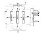
SIMD型プロセッサ1は、図1に示すように、グローバルプロセッサ2、本実施形態では256組の後述するプロセッサエレメント3aからなるプロセッサエレメントブロック3、メモリコントローラ5と接続される外部インターフェース4から構成される。メモリコントローラ5はグローバルプロセッサ2の命令に基づき、メモリ6から演算対象データをプロセッサ内部の入出力用のレジスタフィル31に直接アクセスする。 As shown in FIG. 1, the
まず、メモリコントローラ5につき説明する。図1に示すように、メモリーコントローラ4は、SIMD型プロセッサ1のレジスタファイル31と外部インタフェース4のデータ転送ポートを介して接続されていて、レジスタファイル31からメモリ6へのデータ転送、メモリ6からレジスタファイル31へのデータ転送を行っている。メモリコントローラ5が制御するレジスタは、I/O空間にマッピングされており、グローバルプロセッサ2からの指示に従い、アドレス、クロック、及びリード・ライト制御を出力することでリード、ライト可能となっている。 First, the
グローバルプロセッサ2からメモリコントローラ5へはI/O用のアドレス、データ、コントロール信号がバスを介して与えられる。グローバルプロセッサ2がメモリコントローラ5のいくつかの動作設定レジスタ(図示せず)へ動作方法等のコマンドを設定している。最後にグローバルプロセッサ2は、メモリコントローラ5のスタートレジスタ(図示せず)にスタートコードを書き込むことで、メモリコントローラ5は自動的に設定に従った動作を行う。このように構成することで、プロセッサの命令制御による演算と同時にレジスタファイル31のデータを入出力する。 An I / O address, data, and control signal are given from the
図2は、この発明に用いられるメモリコントローラ5の構成を示したものである。メモリコントローラ5は、メモリ6にデータライトを行うライトバッファ部54と、メモリ6からデータリードを行うリードバッファ部55と、PEレジスタファイルの制御を行っているPE制御部52、メモリ6の制御を行うRAM制御部53、及びシーケンスユニット(SCU)51より構成されている。 FIG. 2 shows the configuration of the
ライトバッファ部54にはSIMD方式プロセッサ1の外部インタフェース4の出力ポートが接続され、リードバッファ部55には外部インタフェース4の入力ポートが接続される。 An output port of the
グローバルプロセッサ2は、図3に示すように、グローバルプロセッサ2、プロセッサエレメントブロック3、外部インタフェース4及びメモリコントローラ5を制御するためのプログラムが格納されたプログラムRAM21、及びこのプログラムRAM21に基づきグローバルプロセッサ2、プロセッサエレメントブロック3、外部インタフェース4、メモリコントローラ5を制御するシーケンスユニット22を備える。具体的には、このシーケンスユニット22は、グローバルプロセッサ2に備えられている後述する算術論理演算器23(以下、「ALU23」という。)等を制御する。 As shown in FIG. 3, the
また、このシーケンスユニット22は、プロセッサエレメントブロック3を構成する後述するレジスタファイル31、及び後述する演算アレイ36を制御する。この演算アレイ36は、マルチプレクサ32、シフト拡張回路33、算術論理演算器34(以下、「ALU34」という)、及びレジスタ35を備える。なお、このグローバルプロセッサ2は、いわゆるSISD型であり、一つの演算命令に対して一つの演算処理を行うものである。 The
さらに、このシーケンスユニット22は、後述するメモリコントローラ5に対してデータ転送のための動作設定用データ及びコマンド等を送る。メモリコントローラ5は、シーケンスユニット22の動作設定用データ及びコマンドに基づき、プロセッサエレメント3aのアドレス指定のためのアドレス制御信号、プロセッサエレメント3aを構成する後述するレジスタ31bにデータのリード/ライトを指示するためのリード/ライト制御信号、クロック信号を与えるためのクロック制御信号を外部インタフェース4に与える。 Further, the
ここで、リード/ライト制御信号のうちライト制御信号とは、演算処理されるデータを後述するデータバス41dより取得して、プロセッサエレメント3aのレジスタ31bに保持させるための信号をいう。一方、リード/ライト制御信号のうちリード制御信号とは、プロセッサエレメント3aのレジスタ31bが保持している演算処理されたデータを、後述するデータバス41dへ与えるようレジスタ31bに指示するための信号をいう。 Here, the write control signal among the read / write control signals refers to a signal for obtaining data to be processed from a
メモリコントローラ5は、グローバルプロセッサ2からのコマンドを受けて、プロセッサエレメントブロック3を構成するプロセッサエレメント3aのアドレスを指定する信号(以下、「アドレス指定信号」という。)を作成し、外部インターフェース4からアドレスバス41aを介してプロセッサエレメント3aの後述するレジスタコントローラ31aヘ送る。また、メモリコントローラ5は、後述するようにプロセッサエレメント3aを構成するレジスタ31bに対して、データのリード/ライトを指示するための信号(以下、「リード/ライト指示信号」という。)を、リード/ライト信号41bを介してプロセッサエレメント3aの後述するレジスタコントローラ31aヘリード/ライト信号が与えられる。また、メモリコントローラ5は、外部インタフェース4からクロック信号41cを介してプロセッサエレメント3aの後述するレジスタコントローラ31aへクロック信号を与える。 Upon receiving a command from the
また、メモリコントローラ5は、上述したように、SIMD型プロセッサ1の外部に設けられたメモリ6に格納されているデータを、本実施形態では8ビットのパラレルデータとして、データバス41dに置く。この8ビットのパラレルデータについては、データに応じて適宜変更しても問題ない。このデータバス41dは、レジスタ31bに保持されている演算処理されたデータが、SIMD型プロセッサ1の外部に設けられたメモリ6に送られる時にも使用される。 Further, as described above, the
なお、メモリ6は演算処理されるデータを格納するとともに、演算処理されたデータを格納するものであり、これらのメモリ6はSIMD型プロセッサ1の内部に設けても問題ない。また、メモリコントローラ5とメモリ6との間のデータ転送についても、本実施形態では8ビットのパラレルデータとして転送されるものとして扱うが、データに応じて適宜変更しても問題ない。なお、メモリコントローラ5が行うその他の動作については後述する。 Note that the memory 6 stores data to be subjected to arithmetic processing and stores data subjected to arithmetic processing, and there is no problem even if these memories 6 are provided inside the
また、グローバルプロセッサ2は、上記シーケンスユニット22からの命令により、算術論理演算を行うALU23、演算データを格納するデータRAM24を備える。さらに、グローバルプロセッサ2は、演算処理されるデータ等を保持するためのレジスタ群25を備える。 In addition, the
このレジスタ群25は、プログラムのアドレスを保持するプログラムカウンタPC、演算処理のデータ格納のための汎用レジスタであるG0〜G3レジスタ、レジスタ待避、復帰時に待避先データRAMのアドレスを保持しているスタックポインタ(SP)、サブルーチンコール時にコール元のアドレスを保持するリンクレジスタ(LS)、同じくIRQ時とNMI時の分岐元アドレスを保持するLI、LNレジスタ、プロセッサの状態を保持しているプロセッサステータスレジスタ(P)を内蔵している。 The register group 25 includes a program counter PC that holds a program address, G0 to G3 registers that are general-purpose registers for storing data for arithmetic processing, and a stack that holds the address of the save destination data RAM at the time of register save and return. Pointer (SP), link register (LS) that holds the address of the caller at the time of a subroutine call, LI and LN registers that hold branch source addresses at the time of IRQ and NMI, and a processor status register that holds the state of the processor (P) is incorporated.
また、レジスタ群25は、プロセッサエレメントブロック3の後述するレジスタ35に接続されており、このレジスタ35との間でシーケンスユニット22の制御によりデータの交換が行われる。 The register group 25 is connected to a later-described
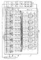
プロセッサエレメントブロック3は、図1及び図3に示すように、レジスタファイル31、マルチプレクサ32、シフト・拡張回路33、算術論理演算器34(以下、「ALU34」という。)、レジスタ35、を一単位とする複数のプロセッサエレメント3aを備える。レジスタファイル31には、1つのプロセッサエレメント3a単位に8ビットのレジスタが32本内蔵されており、本実施形態では256プロセッサエレメント分の組がアレイ構成になっている。レジスタファイル31は1つのプロセッサエレメント(PE)3aごとにR0、R1、R2、...R31と呼ばれているレジスタが内蔵されている。それぞれのレジスタファイル31は演算アレイ36に対して1つの読み出しポートと1つの書き込みポートを備えており、8ビットのリード/ライト兼用のバスで演算アレイ36からアクセスされる。32本のレジスタの内、24本はプロセッサ外部からアクセス可能であり、外部からクロックとアドレス、リード/ライト制御を入力することで任意のレジスタを読み書きできる。 As shown in FIGS. 1 and 3, the
レジスタの外部からのアクセスは1つの外部ポートで各プロセッサエレメント(PE)の1つのレジスタがアクセス可能であり外部から入力されたアドレスでプロセッサエレメント(PE)の番号(0〜255)を指定する。したがって、レジスタアクセスの外部ポートは全部で24組搭載されている。また、外部からのアクセスは偶数のプロセッサエレメント(PE)と奇数のプロセッサエレメント(PE)の1組で16ビットデータとなっており、1回のアクセスで2つのレジスタを同時にアクセスしている。 Access from the outside of the register allows one register of each processor element (PE) to be accessed by one external port, and the number (0 to 255) of the processor element (PE) is designated by an address input from the outside. Therefore, a total of 24 external ports for register access are installed. Access from the outside is 16-bit data in one set of even-numbered processor elements (PE) and odd-numbered processor elements (PE), and two registers are accessed simultaneously by one access.
本実施形態では、プロセッサエレメント3aの数を256個として説明するが、これに限定されるものでなく適宜変更して使用してもよい。このプロセッサエレメント3aには、グローバルプロセッサ2のシーケンスユニット22により、外部インタフェース4に近い順に0から255までのアドレスが割り付けられる。 In the present embodiment, the number of
プロセッサエレメント3aのレジスタファイル31は、レジスタコントローラ31a、2種類のレジスタ31b、31cを備える。本実施形態では、図3及び図4に示すように、一単位のプロセッサエレメント3a毎に、レジスタコントローラ31aとレジスタ31bとを24組備え、さらにレジスタ31cを8個備えている。なお、図4では2組のプロセッサエレメント3aにおけるレジスタファイル31の一部を表しており、図3、4中の1PEとは1つのプロセッサエレメント3aを表している。ここで、本実施形態では、レジスタ31b、31cを8ビットのものとして扱うが、これに限定されるものでなく適宜変更して使用してもよい。 The
レジスタコントローラ31aは、図4に示すように、外部インタフェース4と、上述したアドレスバス41a、リード/ライト信号41b、クロック信号41cを介して接続されている。このレジスタコントローラ31aは、メモリコントローラ5から外部インタフェース4に与えられ、アドレスバス41aを介してアドレス指定信号が送られてくると、そのアドレス指定信号をデコードする。そして、デコードしたアドレスと、自己のプロセッサエレメント3aに割り付けられたアドレスとが一致する場合には、メモリコントローラ5から外部インタフェース4に与えられ、クロック信号41cからのクロック信号に同期して、リード/ライト信号41bを介してメモリコントローラ5から送られてきたリード/ライト指示信号を得る。このリード/ライト指示信号は、レジスタ31bへ与えられる。 As shown in FIG. 4, the
レジスタ31bは、後述するALU34でこれから演算される外部から入力されたデータを保持したり、或いはALU34で演算処理されたデータを外部へ出力するために保持するものであり、いわゆる入力レジスタとしても、或いは出力レジスタとしても機能する。また、演算処理されるデータ、或いは演算されたデータを一時的に保持するといった、後述するレジスタ31cとしての機能も有する。なお、本実施形態では、レジスタ31bは8ビットのデータを保持できるものとして扱うが、データに応じて適宜変更しても問題ない。上述したレジスタコントローラ31aからライト指示信号が与えられると、レジスタ31bは演算処理されるデータをデータバス41dより取得して保持する。一方、レジスタコントローラ31aからリード指示信号が送られてくると、レジスタ31bは保持している演算処理されたデータをデータバス41dへ与える。このデータは外部インタフェース4からメモリコントローラ5のライトバッファ部54に与えられ、ライトバッファ部54からメモリ6へ格納される。 The
また、レジスタ31bは、本実施形態においては8ビットデータをパラレルで転送するデータバス36を介してマルチプレクサ32に接続されている。ALU34で演算処理されるデータ、或いはALU34で演算処理されたデータは、このデータバス36を介して、レジスタ31bとの間で転送される。この転送は、グローバルプロセッサ2のシーケンスユニット22からの指示によって、グローバルプロセッサ2に接続されたリード信号26a、ライト信号26bを介して行われる。具体的には、グローバルプロセッサ2のシーケンスユニット22から、リード信号26aを介してリード指示信号が送られてくると、レジスタ31bはデータバス36を介して送られてきたALU34で演算処理されたデータを保持する。一方、グローバルプロセッサ2のシーケンスユニット22から、ライト信号26bを介してライト指示信号が送られてくると、レジスタ31bは保持している演算処理されるデータをデータバス36へ置く。このデータはALU34へ送られ演算処理される。 The
レジスタ31cは、レジスタ31bより与えられた演算処理されるデータ、或いは演算されたデータがレジスタ31bに与えられる前に、そのデータを一時的に保持するものである。このレジスタ31cは、上述したレジスタ31bと異なり、メモリコントローラ5を介して、メモリ6との間においてデータ転送はしない。 The
演算アレイ36は、マルチプレクサ32シフト/拡張回路33、16ビットALU34及び16ビットのレジスタ35を備えている。このレジスタ35には、16ビットAレジスタ、Fレジスタを内蔵している。 The
プロセッサエレメント(PE)3aの命令による演算は、基本的にレジスタファイル31から読み出されたデータをALU34の片側の入力としてもう片側にはレジスタ35のAレジスタの内容を入力として結果をAレジスタに格納する。したがって、Aレジスタとレジスタファイル31のR0〜R31レジスタとの演算が行われることとなる。レジスタファイル31と演算アレイ36との接続に(7to1)のマルチプレクサ32を置いており、プロセッサエレメント(PE)方向で左に1、2、3つ離れたデータと右に1、2、3つ離れたデータ、中央のデータを演算対象として選択している。また、レジスタファイル31の8ビットのデータはシフト/拡張回路33により任意ビットの左シフトしてALU34に入力される。さらに、図示していない8ビットの条件レジスタ(T)により、プロセッサエレメント3aごとに演算実行の無効/有効の制御をしており、特定のプロセッサエレメント3aだけを演算対象として選択できるように構成している。 The calculation by the instruction of the processor element (PE) 3a basically uses the data read from the
上記したように、マルチプレクサ32は、自己のプロセッサエレメント3aに備えられた上記データバス36に接続されるとともに、両隣3つのプロセッサエレメント3aに備えられたデータバス36にも接続されている。このマルチプレクサ32は7つのプロセッサエレメント3aから1つを選択し、その選択したプロセッサエレメント3aにおけるレジスタレジスタ31b、31cで保持されているデータをALU34へ送る。或いはALU34で演算処理されたデータを、選択したプロセッサエレメント3aにおけるレジスタレジスタ31b、31cへ送る。これによって、隣のプロセッサエレメント3aにおけるレジスタレジスタ31b、31cで保持されているデータを利用した演算処理が可能になり、SIMD型プロセッサ1の演算処理能力を高めることができる。 As described above, the
シフト/拡張回路33は、マルチプレクサ32から送られてきたデータを所定ビットシフトしてALU34へ送る。或いはALU34から送られてきた演算処理されたデータを所定ビットシフトしてマルチプレクサ32へ送る。 The shift /
ALU34は、シフト/拡張回路33から送られてきたデータと、レジスタ35に保持されているデータとに基づき算術論理演算を行う。なお、本実施形態では、ALU34は16ビットのデータに対応できるものとして扱うが、データに応じて適宜変更しても問題ない。演算処理されたデータは、レジスタ35に保持され、シフト/拡張回路33へ転送されたり、或いはグローバルプロセッサ2の汎用レジスタ25へ転送される。 The
次に、外部からプロセッサエレメント3aのレジスタファイル31へのアクセスにつき図4を参照して説明する。この図4では、外部インターフェース4の外部ポートは8ビットのアドレス、ハイレベル時にリード動作をローレベル時にライト動作を示すリード/ライト選択信号、転送のタイミングを示すクロック、転送データである8ビットデータで構成されている。これらの信号はプロセッサの外部インタフェース4に接続され、ここでタイミングおよびバッファリングされ、プロセッサ内部の信号としてアドレス、リード/ライト、クロック、データに変換される。 Next, external access to the
これらの信号はレジスタファイル31の各レジスタに供給されるが、各プロセッサエレメント3a…ごとにアドレスをデコードして各プロセッサエレメント3a…を示すアドレスと一致したプロセッサエレメント3aだけがリード/ライトの動作をおこなう。そのため各プロセッサエレメント3aごとにアドレスのデコードとリード/ライトの制御を行うレジスタコントローラ31aを備える。そして、入出力レジスタ31bには、リード/ライト信号41bから与えられるリードライト指示信号(ライト信号W1、リード信号R1)に基づき、外部インタフェース4と接続されたデータバス41dとデータの転送をおこなう。入出力レジスタ31bは演算アレイ36ともデータの転送をおこなうため、もう一方の入出力ポートを持ち、命令によりグローバルプロセッサ2で作成され、リード信号26a及びライト信号26bから与えられるたライト(W2)、リード(R2)制御信号により、演算アレイ36と接続されたデータバス37(D2)からデータの転送をおこなう。 These signals are supplied to each register of the
図4では2個のプロセッサエレメント3a分の構成だけを図示しているが、図3の256個のプロセッサエレメント3a…の構成と合わせるためには、レジスタコントローラ31aとレジスタファイル31bは256組必要となる。また、256組を選択するためにアドレスのビット幅は8ビットとなっている。従って、プロセッサエレメント3aの数の増減によりアドレスのビット幅も変化することとなる。また、データのビット幅もここでは8ビットとしているが1度に転送するデータ量により変化する。 In FIG. 4, only the configuration for two
このように構成される本実施形態におけるSIMD型プロセッサ1は、以下のような動作を行うため、以下のような利点を得ることができる。 Since the
メモリコントローラ5が、メモリ6に格納されているデータをプロセッサエレメント3aに送る場合、プロセッサエレメント3aに割り付けられたアドレスを指定することにより、1回のクロック信号が入力されるだけで、その指定したプロセッサエレメント3aにデータを送ることができる。例えばデータを偶数番目のプロセッサエレメント3aにだけ転送したい場合には、偶数番目のプロセッサエレメント3aをアドレス指定すればよい。よって、奇数番目のプロセッサエレメント3aに、データを転送する必要がないため、データ転送が高速になり、延いてはデータ処理を高速にすることができる。 When the
また、これとは逆に、レジスタ31bに保持されている演算処理されたデータをメモリ5に転送する場合においても、メモリコントローラ5が、プロセッサエレメント3aに割り付けられたアドレスを指定することにより、1回のクロック信号が入力されるだけで、指定したプロセッサエレメント3aのレジスタ31bに保持されているデータをメモリ6に転送できる。従って、この場合においても、必要なデータのみを転送できるため、データ転送が高速になり、延いてはデータ処理を高速にすることができる。 On the contrary, even when the arithmetically processed data held in the
一つのプロセッサエレメント3aにつき、24個づつ備えられているレジスタ31bは、上述したように、演算処理されるデータを保持したり、或いは演算処理されたデータを保持するものであり、いわゆる入力レジスタとしても、或いは出力レジスタとしても機能する。例えば、メモリコントローラ5からプロセッサエレメント3aに送られるデータ、即ち入力データが56ビットのものであり、プロセッサエレメント3aからメモリコントローラ5に送るデータ、即ち出力データが32ビットのものであり、一時的に保持されるべきデータが80ビットである場合のアプリケーションを考える。この場合、7個のレジスタ31bを56ビットの入力データを保持するものとして利用し(8ビット×7個=56ビット)、4個のレジスタ31bを32ビットの出力データを保持するものとして利用することができる(8ビット×4個=32ビット)。このように、入力データのビット数及び出力データのビット数それぞれのビット数に係わらず、入力データのビット数と出力データのビット数との合計が、8ビット×24個=192ビットを越えなければ、そのアプリケーションの演算実行ができる。 As described above, 24
また、データを一時的に保持するレジスタ31cは、本実施形態では、一つのプロセッサエレメント3aにつき8個づつ備えられている。そのため、8ビット×8個=64ビット分を保持できる。しかし、この例のように、一時的に保持されるべきデータが80ビットである場合には、レジスタ31cだけでは16ビット(=80ビット−64ビット)分のデータが保持できない。この場合においても、本実施形態においてレジスタ31bは、上述したようにデータを一時的に保持する機能も有するため、使用していない11個(=24個−7個−4個)のレジスタ31bのうち、2個(8ビット×2個=16ビット)を一時的なデータ保持のために使用すればよい。 In the present embodiment, eight
このように、レジスタ31bの使用用途が柔軟であるため、データのビット数に柔軟に対応したデータ処理が可能である。このことは、このSIMD型プロセッサ1で演算処理できるアプリケーションの幅が増えることになり、使用用途が広がるという利点がある。 Thus, since the usage of the
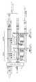
上記した実施の形態においては、外部インタフェース4の外部ポートは外部端子として説明しているが、図5の実施形態のように、転送先のメモリ6とメモリ転送ブロック7が同一チップ上に搭載され、特に外部端子として外部ポートを出力しない場合でも、図3のプロセッサエレメント3a…単位でのアドレスデコードとリード/ライトコントロールにより、同一チップに搭載されたメモリ転送ブロック7等で各プロセッサエレメント3a…の任意のレジスタをアクセスすることが可能である。 In the above embodiment, the external port of the
次に、上記実施の形態の変更例につき図6に従い説明する。図6に示す構成は、図4の基本構成を2つ搭載している。即ち、図3に示す実施の形態では、入出力レジスタ31bは全部で24個あり、8個は演算アレイ36からのみアクセス可能な演算処理用の一時的なデータ保持に使用される演算レジスタ31cである。この2種類のレジスタが合計で32個あるため、例えば、入力データが56ビット、出力データが32ビット、一時的なデータ保持に80ビットが必要なアプリケーションでは、7個の入出力レジスタ31bを外部入力レジスタ用に、4個の入出力レジスタ31bを外部出力レジスタに、8個の演算レジスタ31cと2個の入出力レジスタ31bの合計10個を一時的なデータ保持に割り当てることで実現できる。つまり、入力データと出力データのビット幅の合計が192ビットまでで、一時的なデータ保持のビット幅を加えた合計のビット幅が256ビットまでのアプリケーションであれば自由にレジスタの使用方法を設定して実現できることになる。これに対して、従来のプロセッサでは入力レジスタ、出力レジスタ、演算レジスタが固定のビット幅であったため、いずれかのビット幅を超えるアプリケーションは実現できなかった。 Next, a modified example of the above embodiment will be described with reference to FIG. The configuration shown in FIG. 6 has two basic configurations shown in FIG. That is, in the embodiment shown in FIG. 3, there are 24 input /
(第2の実施形態)
本発明に係るSIMD型プロセッサ1の第2の実施形態を図7を参照して以下説明する。なお、ここでは上述した第1実施形態と異なる点について説明することとし、同じ点については説明を省略する。また、上述した第1実施形態と同じ構成部分については、同一の符号を付する。(Second Embodiment)
A second embodiment of the
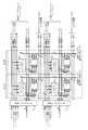
この第2実施形態におけるSIMD型プロセッサ1は、互いに隣り合う2つのプロセッサエレメント3aに偶数番号、奇数番号を割り付けて一組とするとともに、この一組のプロセッサエレメント3aには、同一のアドレスを割り付けていることを特徴とする。さらに、偶数番号が割り付けられたプロセッサエレメント3a用の偶数用データバス46aと、奇数番号が割り付けられたプロセッサエレメント3a用の奇数用データバス46bと、を各組毎のプロセッサエレメント3aにそれぞれ割り当てていることを特徴とする。また、メモリコントローラ4とSIMD型プロセッサ1の外部に設けられたメモリ5、6との間において、データは上記第1実施形態のように8ビットではなく、16ビットがパラレルで転送されることも特徴とする。この16ビットのデータは、偶数番号が割り付けられたプロセッサエレメント3aに与えられる8ビットと、奇数番号が割り付けられたプロセッサエレメント3aに与えられる8ビットとから構成されている。以下、具体的にこの実施形態について説明する。 The
まず、グローバルプロセッサ2からメモリコントローラ5へはI/O用のアドレス、データ、コントロール信号がバスを介して与えられる。グローバルプロセッサ2がメモリコントローラ5のいくつかの動作設定レジスタ(図示せず)へ動作方法等のコマンドを設定している。最後にグローバルプロセッサ2は、メモリコントローラ5のスタートレジスタ(図示せず)にスタートコードを書き込むことで、メモリコントローラ5は自動的に設定に従った動作を行う。 First, an I / O address, data, and control signal are given from the
外部インタフェース4は、メモリコントローラ5からアドレス制御信号を受けると、アドレス指定信号をアドレスバス41aを介してプロセッサエレメントブロック3ヘ送る。これにより、一組のプロセッサエレメント3a、即ち2つのプロセッサエレメント3aが同時にアドレス指定される。レジスタコントローラ31aは、送られてきたアドレス指定信号をデコードし、デコードしたアドレスと、自己に割り付けられたアドレスとが一致する場合には、メモリコントローラ5からクロック信号41cを介して送られてきたクロック信号に同期して、リード/ライト信号45a或いは45bを介してメモリコントローラ4から送られてきたリード/ライト指示信号を得る。具体的には、偶数番号が割り付けられているレジスタコントローラ31aは、偶数用リード/ライト信号45aを介してメモリコントローラ4から送られてきたリード/ライト指示信号を得る。一方、奇数番号が割り付けられているレジスタコントローラ31aは、奇数用リード/ライト信号45bを介してメモリコントローラ4から送られてきたリード/ライト指示信号を得る。このとき一組を構成するプロセッサエレメント3aのレジスタコントローラ31aへ送られるリード/ライト指示信号はそれぞれ異なるものであってもよい。即ち、偶数番号が割り付けられているレジスタコントローラ31aへ送られる指示信号がリード指示であるとき、奇数番号が割り付けられているレジスタコントローラ31aへ送られる指示信号はライト指示であってもよい。そして、このリード/ライト指示信号はレジスタ31bに与えられる。 When receiving the address control signal from the
レジスタコントローラ31aから双方のプロセッサエレメント3aに対し、ライト指示信号が送られてきた場合には、偶数番号が割り付けられたプロセッサエレメント3aのレジスタ31bは、演算処理されるデータ(8ビット)を偶数用データバス46aより取得して保持する。また、奇数番号が割り付けられたプロセッサエレメント3aのレジスタ31bは、演算処理されるデータ(8ビット)を奇数用データバス46bより取得して保持する。一方、レジスタコントローラ31aから双方のプロセッサエレメント3aに対し、リード指示信号が送られてきた場合には、偶数番号が割り付けられたプロセッサエレメント3aのレジスタ31bは、演算処理されたデータ(8ビット)を偶数用データバス46aへ送る。また、奇数番号が割り付けられたプロセッサエレメント3aのレジスタ31bは、演算処理されたデータ(8ビット)を奇数用データバス46bへ送る。 When a write instruction signal is sent from the
このように、一度のアドレス指定により、偶数番号が割り付けられたプロセッサエレメント3aにデータ転送できるとともに、奇数番号が割り付けられたプロセッサエレメント3aにもデータ転送できる。このため、データの転送回数を少なくすることができ、データ転送を高速にできる。よって、データ処理を高速にできる。また、本実施形態においても、上記第1実施形態と同様に、プロセッサエレメント3aをアドレス指定していることより、上記第1実施形態と同様の利点を得ることができる。 As described above, data can be transferred to the
次に、上記実施の形態の変更例につき図8に従い説明する。図8に示す構成は、図7の基本構成を2つ搭載している。即ち、図3に示す実施の形態では、入出力レジスタ31bは全部で24個あり、8個は演算アレイ36からのみアクセス可能な演算処理用の一時的なデータ保持に使用される演算レジスタ31cである。この2種類のレジスタが合計で32個あるため、例えば、入力データが56ビット、出力データが32ビット、一時的なデータ保持に80ビットが必要なアプリケーションでは、7個の入出力レジスタ31bを外部入力レジスタ用に、4個の入出力レジスタ31bを外部出力レジスタに、8個の演算レジスタ31cと2個の入出力レジスタ31bの合計10個を一時的なデータ保持に割り当てることで実現できる。つまり、入力データと出力データのビット幅の合計が192ビットまでで、一時的なデータ保持のビット幅を加えた合計のビット幅が256ビットまでのアプリケーションであれば自由にレジスタの使用方法を設定して実現できることになる。 Next, a modified example of the above embodiment will be described with reference to FIG. The configuration shown in FIG. 8 has two basic configurations shown in FIG. That is, in the embodiment shown in FIG. 3, there are 24 input /
(第3の実施形態)
本発明に係るSIMD型プロセッサ1の第3の実施形態を、図9を参照して以下説明する。上述した第2実施形態においては、プロセッサエレメント3aをアドレス指定しているが、本実施形態はプロセッサエレメント3aの指定をアドレス指定する方式ではなく、ポインタ指定する方式、即ちシリアルアクセスメモリ方式に応用するものである。なお、ここでは上述した第2実施形態と異なる点について説明することとし、同じ点については説明を省略する。また、上述した第2実施形態と同じ構成部分については、同一の符号を付する。(Third embodiment)
A third embodiment of the
まず、グローバルプロセッサ2からメモリコントローラ5へはI/O用のアドレス、データ、コントロール信号がバスを介して与えられる。グローバルプロセッサ2がメモリコントローラ5のいくつかの動作設定レジスタ(図示せず)へ動作方法等のコマンドを設定している。最後にグローバルプロセッサ2は、メモリコントローラ5のスタートレジスタ(図示せず)にスタートコードを書き込むことで、メモリコントローラ5は自動的に設定に従った動作を行う。メモリコントローラ5は、グローバルプロセッサ2のコマンドに基づき、このリセット信号を生成し、外部インタフェース4からリセット信号47を介してプロセッサエレメントブロック3ヘ送る。これにより、レジスタコントローラ31aは、リセットされる。そして、外部インタフェース4に最も近いレジスタコントローラ31aへメモリコントローラ5から外部インタフェース4、クロック信号41cを介してクロック信号が送られる。このクロック信号に同期して、レジスタコントローラ31aは、リード/ライト信号45a或いは45bを介してメモリコントローラ5から送られてきたリード/ライト指示信号を得る。このリード/ライト指示信号は、偶数番号が割り付けられたプロセッサエレメント3aのレジスタ31b、及び奇数番号が割り付けられたプロセッサエレメント3aのレジスタ31bにそれぞれ与えられる。このとき一組を構成するプロセッサエレメント3aのレジスタコントローラ31aへ送られるリード/ライト指示信号は、上記第2実施形態の場合と同様それぞれ異なるものであってもよい。 First, an I / O address, data, and control signal are given from the
これにより、上述した第2実施形態の場合と同様、一度のポインタ指定により、偶数番号が割り付けられたプロセッサエレメント3aにデータ転送できるとともに、奇数番号が割り付けられたプロセッサエレメント3aにもデータ転送できる。このため、データの転送回数を少なくすることができ、データ転送を高速にできる。よって、データ処理を高速にできる。 As a result, as in the case of the second embodiment described above, data can be transferred to the
(第4実施形態)
本発明に係るSIMD型プロセッサ1の第4の実施形態を、図11及び図12を参照して以下説明する。なお、ここでは上述した第1実施形態と異なる点について説明することとし、同じ点については説明を省略する。また、上述した第1実施形態と同じ構成部分については同一の符号を付する。(Fourth embodiment)
A fourth embodiment of the
本実施形態においては、図10に示すように、ラインバッファ61をプロセッサエレメント3aの外部に別途設けることを特徴とする。この図10では、ラインバッファ61を2つ示しているが、ラインバッファ61の数は適宜変更してもよい。このラインバッファ61には、演算処理が終了しているが、注目画素の上下の画素を参照するために必要なデータを保持したり、或いは1ラインの画素数が多い場合にプロセッサエレメント3a…を越える処理画素数を保持することなどに使用される。図10では、入出力レジスタファイル31にラインバッファ61を接続しており、入出力レジスタファイル31に保持されている一部のデータが、このラインバッファ61に送られ保持される。また、ラインバッファ61に保持されているデータは、必要に応じて入出力レジスタファイル31に送られ、演算処理のデータとして使用される。なお、ここで、入出力レジスタファイル31の各ブロックは、図2において横に一列に並んでいる256個のレジスタコントローラ31a及びレジスタ31bを意味する。 In the present embodiment, as shown in FIG. 10, a
上記した実施形態のように、256個のプロセッサエレメント3a…を備えたプロセッサでは、256画素までは内部のレジスタファイル31にデータを置くことが可能である。それを超える画素数の場合、複数の本数のレジスタに同一ラインを分割して保持することになる。上記のようにラインバッファ61を外部に持つことで、256画素ずつラインバッファ61からデータを取り込むことが可能となり、256画素以上のラインでも繰り返し同じ処理を行うことで、画素数をいくらでも増加させることができる。但し、画像数の上限はラインバッファ61の容量で決まる。このように、外部にラインバッファ61を備えることにより、1ラインの画素数が多くなっても容易にその処理を行うことができる。 As in the embodiment described above, a processor having 256
また、入出力レジスタファイル31で保持しているデータを、ラインバッファ61で保持させることで、空いた入出力レジスタファイル31を他の演算処理のために使用でき、演算処理を効率的に行うことができる。即ち、プロセッサエレメント3aのレジスタ31bの容量を越えるデータの処理が可能になる。 Also, by holding the data held in the input /
なお、レジスタファイルの種類に関係なく、ラインバッファ61をプロセッサエレメント3aの外部に別途設けることができる。即ち、図11に示すように、演算処理されるデータを取得して保持するだけの機能を持つ入力レジスタファイル、演算処理されたデータをデータバス41dに出力するだけの機能を持つ出力レジスタファイルに接続して設けてもよい。この場合、出力レジスタファイルに保持されている一部のデータが、ラインバッファ61に送られ保持される。また、ラインバッファ61に保持されているデータは、必要に応じて入力レジスタファイルに送られ、演算処理のデータとして使用される。 Note that the
1 SIMD型プロセッサ
2 グローバルプロセッサ
4 外部インタフェース
5 メモリコントローラ
26aリード信号
26bライト信号
31aレジスタコントローラ
31bレジスタ
34 ALU
41aアドレスバス
41bリード/ライト信号
41dクロック信号
45a偶数用リード/ライト信号
45b奇数用リード/ライト信号
46a偶数用データバス
46b奇数用データバス
47 リセット信号1
Claims (1)
Translated fromJapanese前記指定手段が所定のプロセッサエレメントをアドレス指定することにより、このアドレス指定されたプロセッサエレメントの前記データ保持手段はデータを前記データ転送バスより取得或いは出力することを特徴とするSIMD型プロセッサ。A plurality of processor elements each having a computing means for computing data and data holding means for holding data computed by the computing means and holding data computed by the computing means, and connected to each of the processor elements A data transfer bus, and designation means for designating a predetermined processor element by an address assigned to the processor element,
The SIMD type processor characterized in that the data holding means of the addressed processor element acquires or outputs data from the data transfer bus when the designation means addresses a predetermined processor element.
Priority Applications (1)
| Application Number | Priority Date | Filing Date | Title |
|---|---|---|---|
| JP2006259487AJP4413905B2 (en) | 2006-09-25 | 2006-09-25 | SIMD type processor |
Applications Claiming Priority (1)
| Application Number | Priority Date | Filing Date | Title |
|---|---|---|---|
| JP2006259487AJP4413905B2 (en) | 2006-09-25 | 2006-09-25 | SIMD type processor |
Related Parent Applications (1)
| Application Number | Title | Priority Date | Filing Date |
|---|---|---|---|
| JP25686599ADivisionJP3971535B2 (en) | 1999-09-10 | 1999-09-10 | SIMD type processor |
Publications (2)
| Publication Number | Publication Date |
|---|---|
| JP2007035063Atrue JP2007035063A (en) | 2007-02-08 |
| JP4413905B2 JP4413905B2 (en) | 2010-02-10 |
Family
ID=37794160
Family Applications (1)
| Application Number | Title | Priority Date | Filing Date |
|---|---|---|---|
| JP2006259487AExpired - LifetimeJP4413905B2 (en) | 2006-09-25 | 2006-09-25 | SIMD type processor |
Country Status (1)
| Country | Link |
|---|---|
| JP (1) | JP4413905B2 (en) |
- 2006
- 2006-09-25JPJP2006259487Apatent/JP4413905B2/ennot_activeExpired - Lifetime
Also Published As
| Publication number | Publication date |
|---|---|
| JP4413905B2 (en) | 2010-02-10 |
Similar Documents
| Publication | Publication Date | Title |
|---|---|---|
| EP0539595A1 (en) | Data processor and data processing method | |
| JP3971535B2 (en) | SIMD type processor | |
| US20090238478A1 (en) | Image processing apparatus | |
| JP4408113B2 (en) | Signal processing method | |
| JP3821198B2 (en) | Signal processing device | |
| JP4413905B2 (en) | SIMD type processor | |
| JP4442905B2 (en) | Image data processing method | |
| JP4482356B2 (en) | Image processing method and image processing apparatus using SIMD processor | |
| US20020156992A1 (en) | Information processing device and computer system | |
| JP4451433B2 (en) | Parallel processor | |
| JP2812292B2 (en) | Image processing device | |
| JP3971543B2 (en) | SIMD type processor | |
| US12405794B2 (en) | Signal processing apparatus and non-transitory computer-readable storage medium | |
| JP2003216950A (en) | SIMD type microprocessor for pattern matching etc. | |
| JP4442907B2 (en) | SIMD type processor | |
| JP4294190B2 (en) | Parallel processor and image processing apparatus using the same | |
| JP5369669B2 (en) | SIMD type microprocessor | |
| JP2005148899A (en) | SIMD type processor | |
| JP2009104521A (en) | Parallel processing unit | |
| JPH05143447A (en) | Digital processor and control method for the processor | |
| JP4244619B2 (en) | Image data processing device | |
| JP2005322198A (en) | Data processor | |
| JP2002108833A (en) | Parallel processor and image processing apparatus using the same | |
| EP1050818A1 (en) | Computer memory access | |
| JP2013161325A (en) | Simd (single instruction-stream multiple data-stream) type microprocessor, processor system and data processing method for simd type microprocessor |
Legal Events
| Date | Code | Title | Description |
|---|---|---|---|
| A977 | Report on retrieval | Free format text:JAPANESE INTERMEDIATE CODE: A971007 Effective date:20090217 | |
| A131 | Notification of reasons for refusal | Free format text:JAPANESE INTERMEDIATE CODE: A131 Effective date:20090224 | |
| A521 | Written amendment | Free format text:JAPANESE INTERMEDIATE CODE: A523 Effective date:20090427 | |
| A02 | Decision of refusal | Free format text:JAPANESE INTERMEDIATE CODE: A02 Effective date:20090714 | |
| RD02 | Notification of acceptance of power of attorney | Free format text:JAPANESE INTERMEDIATE CODE: A7422 Effective date:20090715 | |
| RD05 | Notification of revocation of power of attorney | Free format text:JAPANESE INTERMEDIATE CODE: A7425 Effective date:20090909 | |
| A521 | Written amendment | Free format text:JAPANESE INTERMEDIATE CODE: A523 Effective date:20091014 | |
| A911 | Transfer to examiner for re-examination before appeal (zenchi) | Free format text:JAPANESE INTERMEDIATE CODE: A911 Effective date:20091020 | |
| TRDD | Decision of grant or rejection written | ||
| A01 | Written decision to grant a patent or to grant a registration (utility model) | Free format text:JAPANESE INTERMEDIATE CODE: A01 Effective date:20091117 | |
| A01 | Written decision to grant a patent or to grant a registration (utility model) | Free format text:JAPANESE INTERMEDIATE CODE: A01 | |
| A61 | First payment of annual fees (during grant procedure) | Free format text:JAPANESE INTERMEDIATE CODE: A61 Effective date:20091118 | |
| FPAY | Renewal fee payment (event date is renewal date of database) | Free format text:PAYMENT UNTIL: 20121127 Year of fee payment:3 | |
| R150 | Certificate of patent or registration of utility model | Ref document number:4413905 Country of ref document:JP Free format text:JAPANESE INTERMEDIATE CODE: R150 Free format text:JAPANESE INTERMEDIATE CODE: R150 | |
| FPAY | Renewal fee payment (event date is renewal date of database) | Free format text:PAYMENT UNTIL: 20131127 Year of fee payment:4 | |
| EXPY | Cancellation because of completion of term |