JP2007034285A - Thin film transistor manufacturing method - Google Patents
Thin film transistor manufacturing methodDownload PDFInfo
- Publication number
- JP2007034285A JP2007034285AJP2006175257AJP2006175257AJP2007034285AJP 2007034285 AJP2007034285 AJP 2007034285AJP 2006175257 AJP2006175257 AJP 2006175257AJP 2006175257 AJP2006175257 AJP 2006175257AJP 2007034285 AJP2007034285 AJP 2007034285A
- Authority
- JP
- Japan
- Prior art keywords
- manufacturing
- thin film
- film transistor
- transistor substrate
- substrate according
- Prior art date
- Legal status (The legal status is an assumption and is not a legal conclusion. Google has not performed a legal analysis and makes no representation as to the accuracy of the status listed.)
- Withdrawn
Links
Images


Classifications
- G—PHYSICS
- G02—OPTICS
- G02F—OPTICAL DEVICES OR ARRANGEMENTS FOR THE CONTROL OF LIGHT BY MODIFICATION OF THE OPTICAL PROPERTIES OF THE MEDIA OF THE ELEMENTS INVOLVED THEREIN; NON-LINEAR OPTICS; FREQUENCY-CHANGING OF LIGHT; OPTICAL LOGIC ELEMENTS; OPTICAL ANALOGUE/DIGITAL CONVERTERS
- G02F1/00—Devices or arrangements for the control of the intensity, colour, phase, polarisation or direction of light arriving from an independent light source, e.g. switching, gating or modulating; Non-linear optics
- G02F1/01—Devices or arrangements for the control of the intensity, colour, phase, polarisation or direction of light arriving from an independent light source, e.g. switching, gating or modulating; Non-linear optics for the control of the intensity, phase, polarisation or colour
- G02F1/13—Devices or arrangements for the control of the intensity, colour, phase, polarisation or direction of light arriving from an independent light source, e.g. switching, gating or modulating; Non-linear optics for the control of the intensity, phase, polarisation or colour based on liquid crystals, e.g. single liquid crystal display cells
- G02F1/133—Constructional arrangements; Operation of liquid crystal cells; Circuit arrangements
- G02F1/136—Liquid crystal cells structurally associated with a semi-conducting layer or substrate, e.g. cells forming part of an integrated circuit
- H—ELECTRICITY
- H10—SEMICONDUCTOR DEVICES; ELECTRIC SOLID-STATE DEVICES NOT OTHERWISE PROVIDED FOR
- H10D—INORGANIC ELECTRIC SEMICONDUCTOR DEVICES
- H10D86/00—Integrated devices formed in or on insulating or conducting substrates, e.g. formed in silicon-on-insulator [SOI] substrates or on stainless steel or glass substrates
- H10D86/40—Integrated devices formed in or on insulating or conducting substrates, e.g. formed in silicon-on-insulator [SOI] substrates or on stainless steel or glass substrates characterised by multiple TFTs
- H10D86/451—Integrated devices formed in or on insulating or conducting substrates, e.g. formed in silicon-on-insulator [SOI] substrates or on stainless steel or glass substrates characterised by multiple TFTs characterised by the compositions or shapes of the interlayer dielectrics
- H—ELECTRICITY
- H10—SEMICONDUCTOR DEVICES; ELECTRIC SOLID-STATE DEVICES NOT OTHERWISE PROVIDED FOR
- H10D—INORGANIC ELECTRIC SEMICONDUCTOR DEVICES
- H10D86/00—Integrated devices formed in or on insulating or conducting substrates, e.g. formed in silicon-on-insulator [SOI] substrates or on stainless steel or glass substrates
- H10D86/40—Integrated devices formed in or on insulating or conducting substrates, e.g. formed in silicon-on-insulator [SOI] substrates or on stainless steel or glass substrates characterised by multiple TFTs
- H10D86/481—Integrated devices formed in or on insulating or conducting substrates, e.g. formed in silicon-on-insulator [SOI] substrates or on stainless steel or glass substrates characterised by multiple TFTs integrated with passive devices, e.g. auxiliary capacitors
- H—ELECTRICITY
- H10—SEMICONDUCTOR DEVICES; ELECTRIC SOLID-STATE DEVICES NOT OTHERWISE PROVIDED FOR
- H10D—INORGANIC ELECTRIC SEMICONDUCTOR DEVICES
- H10D86/00—Integrated devices formed in or on insulating or conducting substrates, e.g. formed in silicon-on-insulator [SOI] substrates or on stainless steel or glass substrates
- H10D86/40—Integrated devices formed in or on insulating or conducting substrates, e.g. formed in silicon-on-insulator [SOI] substrates or on stainless steel or glass substrates characterised by multiple TFTs
- H10D86/60—Integrated devices formed in or on insulating or conducting substrates, e.g. formed in silicon-on-insulator [SOI] substrates or on stainless steel or glass substrates characterised by multiple TFTs wherein the TFTs are in active matrices
- G—PHYSICS
- G02—OPTICS
- G02F—OPTICAL DEVICES OR ARRANGEMENTS FOR THE CONTROL OF LIGHT BY MODIFICATION OF THE OPTICAL PROPERTIES OF THE MEDIA OF THE ELEMENTS INVOLVED THEREIN; NON-LINEAR OPTICS; FREQUENCY-CHANGING OF LIGHT; OPTICAL LOGIC ELEMENTS; OPTICAL ANALOGUE/DIGITAL CONVERTERS
- G02F1/00—Devices or arrangements for the control of the intensity, colour, phase, polarisation or direction of light arriving from an independent light source, e.g. switching, gating or modulating; Non-linear optics
- G02F1/01—Devices or arrangements for the control of the intensity, colour, phase, polarisation or direction of light arriving from an independent light source, e.g. switching, gating or modulating; Non-linear optics for the control of the intensity, phase, polarisation or colour
- G02F1/13—Devices or arrangements for the control of the intensity, colour, phase, polarisation or direction of light arriving from an independent light source, e.g. switching, gating or modulating; Non-linear optics for the control of the intensity, phase, polarisation or colour based on liquid crystals, e.g. single liquid crystal display cells
- G02F1/133—Constructional arrangements; Operation of liquid crystal cells; Circuit arrangements
- G02F1/136—Liquid crystal cells structurally associated with a semi-conducting layer or substrate, e.g. cells forming part of an integrated circuit
- G02F1/1362—Active matrix addressed cells
- G02F1/1368—Active matrix addressed cells in which the switching element is a three-electrode device
Landscapes
- Physics & Mathematics (AREA)
- Nonlinear Science (AREA)
- Engineering & Computer Science (AREA)
- Microelectronics & Electronic Packaging (AREA)
- Mathematical Physics (AREA)
- Chemical & Material Sciences (AREA)
- Crystallography & Structural Chemistry (AREA)
- General Physics & Mathematics (AREA)
- Optics & Photonics (AREA)
- Thin Film Transistor (AREA)
- Liquid Crystal (AREA)
- Formation Of Insulating Films (AREA)
Abstract
Translated fromJapaneseDescription
Translated fromJapanese本発明は薄膜トランジスタ基板の製造方法に関し、より詳細には、蓄積電極と重なる有機膜の凹凸を除去するための薄膜トランジスタ基板の製造方法に関する。 The present invention relates to a method for manufacturing a thin film transistor substrate, and more particularly to a method for manufacturing a thin film transistor substrate for removing irregularities of an organic film overlapping a storage electrode.
液晶表示装置は単位画素の集合で構成された表示領域を有しており、表示動作をする複数の画素電極がそれぞれの単位画素に形成されている。この画素電極は配線を介して印加される信号によって駆動される。配線には、相互に交差して単位画素領域を定義するゲート線とデータ線とがある。ゲート線には走査信号が印加される。ゲート線はデータ線を介して画素電極に印加される信号を制御する。 The liquid crystal display device has a display area composed of a set of unit pixels, and a plurality of pixel electrodes for performing a display operation are formed in each unit pixel. This pixel electrode is driven by a signal applied via a wiring. The wiring includes a gate line and a data line that intersect with each other to define a unit pixel region. A scanning signal is applied to the gate line. The gate line controls a signal applied to the pixel electrode through the data line.
それぞれの画素は液晶キャパシタを有しており、印加された電圧によって液晶の光透過特性を変化させ通過する光量を調節する役割をする。しかし、液晶表示装置においては液晶キャパシタに印加された電圧を1フレーム間維持しなければならない一方、液晶キャパシタだけではその電圧を十分に維持することが難しい。このような画素の電圧保持能力を補完するために画素毎に液晶キャパシタに並列に接続された蓄積キャパシタが具備される。 Each pixel has a liquid crystal capacitor, and plays a role of adjusting the amount of light passing through by changing the light transmission characteristics of the liquid crystal according to the applied voltage. However, in a liquid crystal display device, the voltage applied to the liquid crystal capacitor must be maintained for one frame, but it is difficult to maintain the voltage sufficiently with only the liquid crystal capacitor. In order to complement the voltage holding capability of such a pixel, a storage capacitor connected in parallel to the liquid crystal capacitor is provided for each pixel.
一方、薄膜トランジスタのデータ配線と半導体層とが一つのマスクを用いてパターニングされた場合、半導体層はチャネル部を除いてはデータ配線の下部にデータ配線と実質的に重なって形成される。したがって、蓄積キャパシタを形成するデータ導電体の下部にも半導体層が存在する。蓄積キャパシタに含まれる半導体層は、MOS(Metal Oxide Semiconductor)キャパシタのように、蓄積キャパシタに印加される電圧によって蓄積キャパシタのキャパシタンス変動を引き起こす。これは、液晶表示装置の表示部でフリッカー現象として確認される。したがって、このキャパシタンス変動を防止するために、蓄積電極と重なる半導体層をエッチングして除去することが行われている。 On the other hand, when the data wiring of the thin film transistor and the semiconductor layer are patterned using one mask, the semiconductor layer is formed to substantially overlap the data wiring under the data wiring except for the channel portion. Therefore, there is also a semiconductor layer below the data conductor that forms the storage capacitor. The semiconductor layer included in the storage capacitor causes a capacitance variation of the storage capacitor due to a voltage applied to the storage capacitor, such as a MOS (Metal Oxide Semiconductor) capacitor. This is confirmed as a flicker phenomenon in the display unit of the liquid crystal display device. Therefore, in order to prevent this capacitance variation, the semiconductor layer overlapping the storage electrode is removed by etching.
ここで、蓄積キャパシタの蓄積電極と対向した他の電極である画素電極を形成するために、保護膜及び有機膜を蒸着した後開口部を形成する際に、スリットマスク等を用いて蓄積電極と重なる部分の有機膜を一部残留させる。この時、この有機膜の表面に凹凸を形成して、エッチングが行われる場合に凹凸によって残留する保護膜及びゲート絶縁膜がエッチングされたりエッチングが過度に進んだりしてゲート絶縁膜までエッチングされ、蓄積電極が露出されて画素電極と短絡される。また、このような凹凸は、蓄積キャパシタのキャパシタンスの位置ごとの偏差を生じさせる原因となり、液晶表示装置のフリッカー現象として確認される。
本発明が解決しようとする技術的課題は、蓄積電極と重なる有機膜の凹凸を除去するための薄膜トランジスタ基板の製造方法を提供することにある。 A technical problem to be solved by the present invention is to provide a method of manufacturing a thin film transistor substrate for removing irregularities of an organic film overlapping a storage electrode.
前記技術的課題を達成するための本発明の一実施形態による薄膜トランジスタ基板の製造方法は、蓄積電極が形成されている基板上に保護膜及び前記保護膜を覆う有機膜を形成することと、前記蓄積電極と重なった領域の前記有機膜を一部除去し、その底面が凹凸パターンを有する凹部を形成することと、前記底面の凹凸パターンを平坦化すること及び前記保護膜上面の前記平坦化された有機膜を除去し、前記凹部が前記保護膜上面まで延長された開口部を形成することを含む。 A method of manufacturing a thin film transistor substrate according to an embodiment of the present invention for achieving the technical problem includes forming a protective film and an organic film covering the protective film on a substrate on which a storage electrode is formed, A part of the organic film in a region overlapping with the storage electrode is removed, a concave portion having a concavo-convex pattern on the bottom surface thereof is formed, and the concavo-convex pattern on the bottom surface is flattened, and the top surface of the protective film is flattened. And removing the organic film to form an opening in which the recess extends to the upper surface of the protective film.
その他実施形態の具体的な事項は詳細な説明及び図面に含まれている。 Specific matters of the other embodiments are included in the detailed description and the drawings.
前記したような本発明の薄膜トランジスタ基板の製造方法によれば、一つまたはそれ以上の効果がある。 According to the method of manufacturing a thin film transistor substrate of the present invention as described above, there are one or more effects.
第一に、スリットマスクを用いて保護膜上に残留した有機膜の表面で凹凸を除去するため、コンタクトホールを形成するためのエッチングで保護膜及びゲート絶縁膜までエッチングされなくなり、これによって画素電極と蓄積電極との短絡を防止することができる。 First, since the unevenness is removed on the surface of the organic film remaining on the protective film using the slit mask, the protective film and the gate insulating film are not etched by the etching for forming the contact hole, thereby the pixel electrode. And the storage electrode can be prevented from being short-circuited.
第二に、保護膜上に残留した有機膜の凹凸を除去するため、蓄積キャパシタのキャパシタンスの位置ごとの偏差を無くすことができ、液晶表示装置のフリッカー現象を防止することができる。 Second, since the unevenness of the organic film remaining on the protective film is removed, the deviation of the capacitance of the storage capacitor for each position can be eliminated, and the flicker phenomenon of the liquid crystal display device can be prevented.
明細書全体にかけて同一参照符号は同一構成要素を指称する。 Like reference numerals refer to like elements throughout the specification.
以下、添付した図面を参照して本発明の一実施形態による薄膜トランジスタ基板の製造方法について説明する。 Hereinafter, a method of manufacturing a thin film transistor substrate according to an embodiment of the present invention will be described with reference to the accompanying drawings.
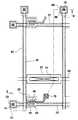
まず、図1A及び図1Bを参照して本発明の一実施形態による薄膜トランジスタ基板の単位画素構造について詳細に説明する。 First, a unit pixel structure of a thin film transistor substrate according to an embodiment of the present invention will be described in detail with reference to FIGS. 1A and 1B.
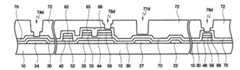
図1Aは、本発明の一実施形態による薄膜トランジスタ基板製造方法によって製造された薄膜トランジスタ基板のレイアウト図である。図1Bは、図1AのB−B’線に沿った断面図である。 FIG. 1A is a layout diagram of a thin film transistor substrate manufactured by a method of manufacturing a thin film transistor substrate according to an embodiment of the present invention. 1B is a cross-sectional view taken along line B-B ′ of FIG. 1A.
まず、本発明の一実施形態においては、絶縁基板10上にゲート信号を伝達する複数のゲート配線が形成されている。ゲート配線22、24、26、27、28は、横方向に延びているゲート線22、ゲート線22の端に接続されていて外部からのゲート信号の印加を受けてゲート線に伝達するゲート終端24、ゲート線22に接続されて突起状に形成された薄膜トランジスタのゲート電極26、ゲート線22と平行に形成されている蓄積電極27及び蓄積電極線28を含む。蓄積電極線28は画素領域を横切って横方向に延びており、蓄積電極線28に比べて幅が広く形成されている蓄積電極27が接続される。蓄積電極27を広く形成することによって蓄積電極27が画素電極82と重なる面積を広げて蓄積容量を増加させる。蓄積電極27は、後述する画素電極82と重なって画素の電荷保存能力を向上させる蓄積キャパシタ90を形成する。このような蓄積電極27及び蓄積電極線28の形態及び配置等は多様な形態に変形可能である。 First, in one embodiment of the present invention, a plurality of gate wirings for transmitting gate signals are formed on the
蓄積キャパシタ90は、液晶キャパシタ(図示せず)に印加された電圧が1フレーム間保持電圧を維持するために液晶キャパシタに並列に接続されている。蓄積キャパシタ90は、蓄積電極27、その上に重なったゲート絶縁膜30、保護膜70及び画素電極82を含む。 The
ゲート絶縁膜30は無機物質である窒化シリコン(SiNx)等で構成される。 The
保護膜70は、例えば無機物質である窒化シリコン(SiNx)、またはプラズマ化学気相蒸着(Plasma enhanced Chemical Vapor Deposition;PECVD)によって形成されるa−Si:C:O、a−Si:O:F等の低誘電率絶縁物質等で形成されるようにしてもよく、その厚さは0.2μmであってもよい。 The
保護膜70上部には蓄積キャパシタ90の他方電極である画素電極82が形成されており、これはドレイン電極66と接続されて、蓄積キャパシタ90が液晶キャパシタ(図示せず)と並列に接続される。画素電極82はITOまたはIZOで構成されている。 A
ここで、蓄積電極27等のゲート配線22、24、26、27、28は、クロム(Cr)、アルミニウム(Al)、モリブデン(Mo)またはモリブデンタングステン(MoW)等の金属単一膜や、必要によってはアルミニウム合金(AlNd)及びクロム金属の二重層、アルミニウム合金(AlNd)及びタングステン金属の二重層や三重層で構成されるようにすればよい。 Here, the
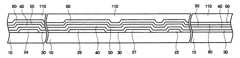
基板10、ゲート配線22、24、26、27、28上には窒化シリコン(SiNx)等で構成されたゲート絶縁膜30が形成されている。 A
ゲート絶縁膜30上には水素化非晶質シリコンまたは多結晶シリコン等の半導体で構成された半導体層42、44、48が形成されている。半導体層42、44、48の上部にはシリサイド等のn型不純物が高農度でドーピングされているn+水素化非晶質シリコン等の物質からなったオーミックコンタクト層52、55、56、58が形成されている。特に、ソース電極65及びドレイン電極66下のオーミックコンタクト層55、56は、下の半導体層44とコンタクト抵抗を減らす役割をする。 On the
オーミックコンタクト層52、55、56、58上にはデータ配線62、65、66、68が形成されている。データ配線62、65、66、68は縦方向に形成されてゲート線22と交差して画素を定義するデータ線62、データ線62の分枝でありオーミックコンタクト層55の上部まで延長されているソース電極65、データ線62の一端側に接続され外部からの画像信号の印加を受けるデータ終端68、及びソース電極65と分離されており、ゲート電極26または薄膜トランジスタのチャネル部に対してソース電極65の反対側オーミックコンタクト層56上部に形成されているドレイン電極66を含む。
ソース電極65は半導体層44と少なくとも一部分が重なっている。ドレイン電極66は、ゲート電極26を中心にしてソース電極65と対向して半導体層40と少なくとも一部分が重なる。 The
オーミックコンタクト層52、55、56、58は、データ配線62、65、66、68と完全に同一形態を有している。半導体層42、44、48は、薄膜トランジスタのチャネル部を除いてデータ配線62、65、66、68及びオーミックコンタクト層52、55、56、58と同一形状をしている。すなわち、薄膜トランジスタのチャネル部でソース電極65とドレイン電極66とが分離されており、ソース電極65下部のオーミックコンタクト層55とドレイン電極66下部のオーミックコンタクト層56とも分離されている。一方、薄膜トランジスタ用半導体層44は、ソース電極65とドレイン電極66とが分離されている領域で切れておらず接続されており、薄膜トランジスタのチャネルを生成する。 The
データ配線62、65、66、68及びこれらが遮らない半導体層44上部には保護膜70が形成されている。保護膜70は、例えば無機物質である窒化シリコン(SiNx)またはプラズマ化学気相蒸着(Plasma enhanced Chemical Vapor Deposition;PECVD)で形成されるa−Si:C:O、a−Si:O:F等の低誘電率絶縁物質等で形成されることができる。また、保護膜70を有機物質で形成する場合には、ソース電極65とドレイン電極66との間の半導体層44が露出された部分に保護膜70の有機物質が接触することを防止するために、有機膜の下部に窒化シリコン(SiNx)または酸化シリコン(SiO2)で構成された絶縁膜(図示せず)がさらに形成されるようにしてもよい。A
蓄積電極27上部の保護膜70は、下部のゲート絶縁膜30と共に蓄積電極27と画素電極82との間に位置して蓄積キャパシタ90のキャパシタンスを形成する蓄積容量を形成する。 The
保護膜70上部には有機膜72が形成されている。有機膜72は平坦化特性が優れ且つ感光性(photosensitivity)を有する有機物質、例えばPFCB(PerFluoroCycloButane)、BCB(BenzoCycloButene)またはアクリル等で形成されるようにしてもよい。 An
有機膜72にはドレイン電極66、データ線終端68をそれぞれ露出するコンタクトホール76、78が形成されている。保護膜70とゲート絶縁膜30とにはゲート線終端24を露出するコンタクトホール74が形成されている。ここで、ドレイン電極66、データ線終端68及びゲート終端24を露出するコンタクトホール(76、78、74)は階段型プロファイルを有するようにしてもよい。また、蓄積電極27上部の有機膜が除去されて保護膜70を露出する開口部77が形成されている。一方、コンタクトホール74、76、78及び開口部77が形成されている有機膜72上には、コンタクトホール76を介してドレイン電極66と接続された画素電極82が形成されている。画素電極82は開口部77を介して保護膜70と接続され、蓄積キャパシタ90の反対電極を形成する。蓄積キャパシタ90は画素電極82を介して液晶キャパシタ(図示せず)と並列に接続されている。また、有機膜72上にはコンタクトホール74、78を介してそれぞれゲート終端24及びデータ終端68と接続されている補助ゲート終端84及び補助データ終端88が形成されている。画素電極82と補助ゲート及びデータ終端84、88とはITOまたはIZOで構成されている。 Contact holes 76 and 78 exposing the
以下、本発明の一実施形態による薄膜トランジスタ基板の製造方法について図1A及び図1B、並びに図2Aないし図10Eを参照しながら説明するようにする。 Hereinafter, a method of manufacturing a thin film transistor substrate according to an embodiment of the present invention will be described with reference to FIGS. 1A and 1B and FIGS. 2A to 10E.
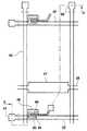
まず、図2A及び図2Bに示したように、絶縁基板10上に導電層を積層しフォトエッチングすることによってゲート配線22、24、26、27、28を形成する。 First, as shown in FIGS. 2A and 2B, gate wirings 22, 24, 26, 27, and 28 are formed by laminating a conductive layer on the insulating
ここで、クロム(Cr)、アルミニウム(Al)、モリブデン(Mo)またはモリブデンタングステン(MoW)等の金属単一膜や、必要によってはアルミニウム合金(AlNd)及びクロム金属の二重層、アルミニウム合金(AlNd)及びタングステン金属の二重層や三重層ゲート金属をスパッタリング方法によって形成し、その上部にフォトレジストを塗布して、マスクを設け露光して現像する。その後、湿式エッチングによって前記フォトレジストを剥離することによって、ゲート配線22、24、26、27、28が形成される。 Here, a single metal film such as chromium (Cr), aluminum (Al), molybdenum (Mo), or molybdenum tungsten (MoW), or a double layer of aluminum alloy (AlNd) and chromium metal as required, an aluminum alloy (AlNd) ) And a tungsten metal double layer or a triple layer gate metal are formed by a sputtering method, a photoresist is applied thereon, a mask is provided, and exposure and development are performed. Thereafter, the photoresist is removed by wet etching to form gate wirings 22, 24, 26, 27, and 28.
これによって図2A及び図2Bに示したようにゲート線22、ゲート電極26、ゲート終端24、蓄積電極27及び蓄積電極線28を含むゲート配線22、24、26、27、28が形成される。 As a result, as shown in FIGS. 2A and 2B, gate wirings 22, 24, 26, 27, 28 including the
続いて、図3に示したように窒化シリコンで構成されたゲート絶縁膜30、真性非晶質シリコン層40及びドーピングされた非晶質シリコン層50を例えば化学気相蒸着法を利用してそれぞれ150nmないし500nm、50nmないし200nm、30nmないし60nmの厚さに連続的に蒸着する。 Subsequently, as shown in FIG. 3, the
続いて、ドーピングされた非晶質シリコン層50上にスパッタリング方法などによって導電層60を積層する。 Subsequently, a
続いて、導電層60の上部に感光膜110を塗布する。 Subsequently, a
続いて、図4A及び図4Bを参照すると、マスクを通して感光膜110に光を照射した後、現像し、図4Bに示したように、感光膜パターン112、114を形成する。感光膜パターン112、114のうち薄膜トランジスタのチャネル部、すなわちソース電極65とドレイン電極66との間に位置した第1部分114は、データ配線部、すなわちデータ配線が形成される部分に位置した第2部分112より厚さが薄くなるようにし、チャネル部とデータ配線部とを除いたその他部分の感光膜をすべて除去する。ここで、蓄積電極27と重なる感光膜も除去する。この時、チャネル部に残っている感光膜114の厚さとデータ配線部に残っている感光膜112の厚さの比は後述するエッチング工程における工程条件によって異なるようにしなければならないが、第1部分114の厚さを第2部分112の厚さの1/2以下にすることが好ましく、例えば、400nm以下であることが好ましい。 4A and 4B, the
なお、位置によって感光膜の厚さを異ならせる方法には種々の方法があり、光透過量を調節するために主にスリット(slit)や格子状のパターンを形成したり半透明膜を用いる。 There are various methods for varying the thickness of the photosensitive film depending on the position. In order to adjust the light transmission amount, a slit or a lattice pattern is mainly formed, or a translucent film is used.
このようなマスクを通して感光膜に光を照射することにより、光に直接露出する部分においては高分子が完全に分解されるが、スリットパターンや半透明膜が形成されている部分においては光の照射量が少ないため高分子は完全分解されず、また、遮光膜によって遮られた部分においては高分子がほとんど分解されない。続いて感光膜を現像すると、高分子分子が分解されない部分だけが残り、少量の光が照射された中央部分においては、光が全く照射されない部分より薄い厚さの感光膜を残すことができる。この時、露光時間を長くすればすべての分子が分解されるので、そのようにならないようにしなければならない。 By irradiating light to the photosensitive film through such a mask, the polymer is completely decomposed in the part exposed directly to the light, but the light is irradiated in the part where the slit pattern or the semitransparent film is formed. Since the amount is small, the polymer is not completely decomposed, and the polymer is hardly decomposed at the portion blocked by the light shielding film. Subsequently, when the photosensitive film is developed, only the part where the polymer molecules are not decomposed remains, and in the central part irradiated with a small amount of light, the photosensitive film having a thinner thickness than the part where no light is irradiated can be left. At this time, if the exposure time is lengthened, all the molecules are decomposed, so this must be avoided.
続いて、導電層60に対するエッチングを行う。この時のエッチングは湿式エッチングによって行うことができ、エッチングに用いる液体は酢酸、硝酸、燐酸の混合液を用いることができる。 Subsequently, the
このようにすれば、図5に示したように、チャネル部及びデータ配線部の導電層パターン62、64、68だけが残り、チャネル部及びデータ配線部を除いたその他部分の導電層60はすべて除去され、その下部のドーピングされた非晶質シリコン層50が露出される。この時残った導電層パターン62、64、67、68は、ソース及びドレイン電極65、66が分離されず接続している点以外ば、データ配線62、65、66、68の形態と同じである。 In this way, as shown in FIG. 5, only the
続いて、図6に示したように、チャネル部とデータ配線部を除いた他の部分における露出している非晶質シリコン層50及びその下部の真性非晶質シリコン層40を感光膜の第1部分114と共に乾式エッチング方法によって同時に除去する。この時のエッチングは、感光膜パターン112、114とドーピングされた非晶質シリコン層50及び真性非晶質シリコン層40とが同時にエッチングされゲート絶縁膜30がエッチングされない条件下で行い、半導体層42、44、48及びオーミックコンタクト層50、52、58を形成する。特に感光膜パターン112、114のエッチングレートと真性非晶質シリコン層40のエッチングレートがほとんど同じとなる条件下でエッチングすることが好ましい。例えば、SF6とHClとの混合ガスや、SF6とO2との混合ガスを用いると、ほとんど同じ厚さでこれら二つの膜をエッチングすることができる。感光膜パターン112、114のエッチングレートと真性非晶質シリコン層40のエッチングレートが等しい場合、第1部分114の厚さは、真性非晶質シリコン層40の厚さとドーピングされた非晶質シリコン層50の厚さの合計と同じであるかそれより小さくなければならない。このようにすれば、図7に示したように、チャネル部の第1部分114が除去されてソース/ドレイン用パターン64が露出されて、その他部分のドーピングされた非晶質シリコン層50及び真性非晶質シリコン層40が除去されて、その下部のゲート絶縁膜30が露出される。一方、データ配線部の第2部分112もエッチングされるので厚さが薄くなる。Subsequently, as shown in FIG. 6, the exposed
続いて、アッシング(ashing)を介してチャネル部のソース/ドレイン用パターン64の表面に残っている感光膜残滓を除去する。 Subsequently, the photosensitive film residue remaining on the surface of the source /
続いて、図7に示したように、チャネル部のソース/ドレイン用パターン64をエッチングすることによって除去する。このエッチング工程はエッチング液を用いる湿式エッチングで行われる。 Subsequently, as shown in FIG. 7, the source /
続いて、ドーピングされた非晶質シリコンで構成されたオーミックコンタクト層55、56をエッチングする。この時、乾式エッチングを用いるようにしてもよい。エッチングガスの例としては、CF4とHClとの混合ガスやCF4とO2との混合ガスを挙げることができ、CF4とO2とを用いると、均一な厚さで真性非晶質シリコンで構成された半導体層44を残すことができる。この時、半導体層44の一部が除去されて厚さが薄くなり得、感光膜パターンの第2部分112もある程度の厚さでエッチングされ得る。この時のエッチングはゲート絶縁膜30がエッチングされない条件で行なわなければならなく、第2部分112がエッチングされ、その下部のデータ配線62、65、66、67、68が露出されることがないように感光膜パターンが厚いのが好ましいことはもちろんである。Subsequently, the ohmic contact layers 55 and 56 made of doped amorphous silicon are etched. At this time, dry etching may be used. Examples of the etching gas include a mixed gas of CF4 and HCl and a mixed gas of CF4 and O2. When CF4 and O2 are used, an intrinsic amorphous film with a uniform thickness can be used. The
このようにすれば、ソース電極65とドレイン電極66とを分離しながらデータ配線65、66とその下部のオーミックコンタクト層55、56とが完成する。 In this way, the data lines 65 and 66 and the ohmic contact layers 55 and 56 below the data lines 65 and 66 are completed while separating the
続いて、図8に示したようにデータ配線部に残っている感光膜第2部分112を除去する。 Subsequently, as shown in FIG. 8, the second
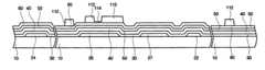
続いて、図9に示したように、例えばプラズマ化学気相蒸着等で形成されるa−Si:C:O、a−Si:O:F等の低誘電率絶縁物質、または無機物質である窒化シリコン(SiNx)等を堆積して保護膜70を形成した後、PFCB、BCBまたはアクリル系物質等を塗布し有機膜72を形成する。この時、堆積される保護膜70は0.15ないし0.25μmであるようにしてもく、積層される有機膜72は2.5ないし3.5μmであるようにしてもよい。有機膜72の厚さは、ドレイン電極66と画素電極82との間の寄生容量を減らしながら有機膜72の透過率の減少を最小化することができる3.0μmが好ましい。 Subsequently, as shown in FIG. 9, for example, a low dielectric constant insulating material such as a-Si: C: O or a-Si: O: F formed by plasma chemical vapor deposition or the like, or an inorganic material. After depositing silicon nitride (SiNx) or the like to form the
図10A及び図10Bを参照すると、有機膜72上に光マスク100を配置する。光マスク100は透明な基板110とその下部の遮光層120とで構成され、遮光層120の幅が所定値以上である不透明領域Cと、一定幅以上遮光層120がない透明領域Aと、遮光層120の幅及び/または間隔が所定値以下であるスリット型の半透明領域Bとを含む。光マスク100は、透明領域Aがゲート終端24、ドレイン電極66、蓄積電極27及びデータ終端68と重なる有機膜72の部分に対応するように配置される。 Referring to FIGS. 10A and 10B, the optical mask 100 is disposed on the
続いて、光マスク100を介して露光し、現像して、蓄積電極27と重なる領域の凹部77bを形成する。光マスク100の半透明膜Bを用いて形成される凹部77bにおいては、拡大図に図示したように凹部77bの底面に一定な高さ差gを有する凹凸パターンが形成される。凹部77b及び保護膜70上に有機膜72が残留する。ここで残留する有機膜72の厚さは0.5ないし1.5μmであるようにしてもよい。言い換えると、凹部77bの底面と保護膜70の上部面との間の厚さは0.5ないし1.5μmであるようにしてもよい。好ましくは後続する有機膜パターン74b、76b、78bを介して保護膜70及び/またはゲート絶縁膜30をエッチングする段階で、蓄積電極27と重なる保護膜70及びゲート絶縁膜30を保護することができるように1.0μmであるようにしてもよい。有機膜72を残留させる理由は、有機膜72が後述するエッチングによってその下部に存在する保護膜70及びゲート絶縁膜30を保護することができるからである。 Subsequently, exposure is performed through the optical mask 100 and development is performed to form a
またゲート終端24、ドレイン電極66及びデータ終端68と重なる領域の保護膜70が露出される有機膜パターン74b、76b、78bを形成する。この時、有機膜パターン74b、76b、78bは階段型のプロファイルを形成するようにしてもよい。 Further,
本発明の実施形態ではスリットマスクを用いて有機膜パターンを形成することを例に挙げるが、格子パターンまたは半透明膜を含むマスクを用いるようにしてもよい。 In the embodiment of the present invention, an example of forming an organic film pattern using a slit mask is taken as an example, but a mask including a lattice pattern or a translucent film may be used.
この時、スリット間に位置したパターンの線幅やパターン間の間隔、すなわちスリットの幅は、露光時用いる露光機の分解能より小さいことが好ましい。半透明膜を用いる場合には、マスクを製作する時、透過率を調節するために他の透過率を有する薄膜を用いたり厚さが異なった薄膜を用いたりすればよい。 At this time, it is preferable that the line width of the pattern positioned between the slits and the interval between the patterns, that is, the width of the slit is smaller than the resolution of the exposure machine used during exposure. When a translucent film is used, when manufacturing a mask, a thin film having another transmittance or a thin film having a different thickness may be used in order to adjust the transmittance.
続いて図11に示したように、凹部(図10Bの77b参照)の底面に形成された凹凸パターンに対して乾式エッチングを行う。この時、凸部が凹部よりもっと多くエッチングされるため、高さの差を減少させ、凹部はほとんど影響がない程度に減少する。凹部77cの下部に形成された保護膜70を露出しないながら、図11の拡大図に示したように、凹部77cの底面に形成された凹凸の高さ差をgからhに減らすことができるように凸部をエッチングする(ただし、h<g)。ここで前記エッチングは乾式エッチングで行われ、エッチングで用いられるガスはSF6とO2との混合ガスまたはSF6とN2との混合ガスであるようにしてもよい。このように凹凸が緩和されることによって、後続するアッシングによる平坦化工程時間を減少することができる。Subsequently, as shown in FIG. 11, dry etching is performed on the concave / convex pattern formed on the bottom surface of the concave portion (see 77b in FIG. 10B). At this time, since the convex part is etched more than the concave part, the difference in height is reduced, and the concave part is reduced to an extent that there is almost no influence. As shown in the enlarged view of FIG. 11, the height difference of the unevenness formed on the bottom surface of the recess 77 c can be reduced from g to h without exposing the
この時、ゲート終端24、データ終端68及びドレイン電極66と重なる有機膜パターン74c、76c、78cを介して、その下部の保護膜70の一部がエッチングされたり保護膜全部がエッチングされるたりする場合がある。 At this time, part of the
続いて図12に示したように、凹部(図11の77c参照)の底面の凹凸をアッシング工程を介して底面が平坦化された凹部77dを形成する。これを詳細に説明すると、高温で酸素プラズマを用いて高分子有機物で構成された凹部(図11の77c参照)の凹凸を酸素プラズマの副産物であるO*(酸素ラジカル)と反応させれば、有機物質が分解しながらCO2とH2Oとが生成される。この時、凹部(図11の77c参照)の底面で形成された凹凸の凸部が凹部より更に分解されて除去されるので、凹部77dの底面が実質的に平坦化される。この時、アッシング工程の効率を改善するために水素(H2)及び窒素(N2)の混合ガス等を用いることができる。ここで酸素プラズマを用いたアッシングは、保護膜70より有機膜72に対して選択比が良いので、凹部77bと保護膜70との間の有機膜72以外に保護膜70ではほとんど影響を受けない。この時、アッシングは保護膜70が露出されないように調節する。Subsequently, as shown in FIG. 12, a concave portion 77d having a flat bottom surface is formed through an ashing process on the concave and convex portions on the bottom surface of the concave portion (see 77c in FIG. 11). Explaining this in detail, if the unevenness of the recess (see 77c in FIG. 11) made of a polymer organic substance is reacted with O * (oxygen radical), which is a byproduct of oxygen plasma, using oxygen plasma at high temperature, CO2 and H2 O are produced while the organic substance is decomposed. At this time, since the concave and convex portions formed on the bottom surface of the concave portion (see 77c in FIG. 11) are further disassembled and removed from the concave portion, the bottom surface of the concave portion 77d is substantially flattened. At this time, a mixed gas of hydrogen (H2 ) and nitrogen (N2 ) can be used to improve the efficiency of the ashing process. Here, the ashing using oxygen plasma has a better selection ratio than the
このような凹凸を除去することによって後述するエッチング工程で蓄積電極27と重なる保護膜70及びゲート絶縁膜30のエッチングを防止することができ、エッチングが更に行われ、蓄積電極27が露出することを防止することができる。また、凹部77bの底面を平坦化することによって、蓄積キャパシタの蓄積容量を形成する保護膜70上に有機膜72の凹凸がほとんど無くなり、位置が変わっても蓄積キャパシタのキャパシタンスが一定になる。 By removing such irregularities, it is possible to prevent etching of the
続いて図13に示したように、図11の実施形態で用いたエッチングガス体を用いて凹部(図12の77d)を更に延長して蓄積電極27と重なる保護膜70を露出する開口部77を形成する。また、図11の実施形態で用いたエッチングガスを用いてデータ配線66、68を露出するコンタクトホール76、78、及びゲート終端24を露出するコンタクトホール74を形成する。ここで、凹部(図12の77d参照)と保護膜70との間の有機膜72のみエッチングして、保護膜70をエッチングしないように調節するようにすればよい。 Subsequently, as shown in FIG. 13, the recess 77 (77 d in FIG. 12) is further extended using the etching gas body used in the embodiment of FIG. 11 to expose the
本発明の実施形態では蓄積電極と重なる保護膜上に有機膜を除去したが、保護膜上に薄い有機膜を残留するようにしてもよい。また、蓄積電極と画素電極との間の距離を狭め、蓄積キャパシタのキャパシタンスを増加させるためにエッチングを更にに行い保護膜の一部を除去したり、保護膜全部を除去したりして、保護膜の一部及びゲート絶縁膜またはゲート絶縁膜に対してのみ蓄積キャパシタの蓄積容量を形成しても構わない。 In the embodiment of the present invention, the organic film is removed on the protective film overlapping the storage electrode, but a thin organic film may remain on the protective film. In addition, in order to reduce the distance between the storage electrode and the pixel electrode and increase the capacitance of the storage capacitor, further etching is performed to remove a part of the protective film or to remove the entire protective film. The storage capacitor of the storage capacitor may be formed only for part of the film and the gate insulating film or the gate insulating film.
最後に、図1A及び図1Bに示したように、40nmないし50nmの厚さのITO層を体積しフォトエッチングして開口部77を介して蓄積電極27と重なった保護膜70上に画素電極82を形成する。また、コンタクトホール74、76、78を介してドレイン電極66、保護膜70と接続された画素電極82、ゲート終端24と接続された補助ゲート終端84及びデータ終端68と接続された補助データ終端88を形成する。 Finally, as shown in FIGS. 1A and 1B, the ITO layer having a thickness of 40 nm to 50 nm is volume-etched and photo-etched to form the
保護膜70上に画素電極82を形成することによって、蓄積電極27、ゲート絶縁膜30、保護膜70及び画素電極82を含む蓄積キャパシタが完成する。ここで、蓄積キャパシタの一側電極である画素電極82は蓄積キャパシタの蓄積電極27と反対側の電極を形成する。また、蓄積キャパシタは画素電極82が延長されてドレイン電極66と接続されて液晶キャパシタ(図示せず)と並列に接続される。 By forming the
一方、ITOを積層する前の予熱(pre−heating)工程で用いるガスには窒素を用いることが好ましく、これは、コンタクトホール74、76、78を介して露出した金属膜24、66、68の上部に金属酸化膜が形成されることを防止するためである。 On the other hand, it is preferable to use nitrogen as a gas used in the pre-heating process before laminating the ITO, and this is because the
本発明の実施形態では4マスク工程で例を挙げて説明したが、データ配線と半導体層とを一つのマスクにして薄膜トランジスタ基板を製造する工程であれば、これに限定されるわけではない。 In the embodiment of the present invention, the four mask process is described as an example, but the present invention is not limited to this as long as it is a process for manufacturing a thin film transistor substrate using the data wiring and the semiconductor layer as one mask.
本発明の実施形態ではデータ配線が単一層である例を挙げて説明したが、ゲート配線またはデータ配線は二重層または三重層であってもよく、これに限定されるわけではない。 In the embodiment of the present invention, an example in which the data wiring is a single layer has been described. However, the gate wiring or the data wiring may be a double layer or a triple layer, and is not limited thereto.
以上添付した図面を参照して本発明の実施形態を説明したが、本発明が属する技術分野で通常の知識を有する者は、本発明がその技術的思想や必須な特徴を変更せずに他の具体的な形態で実施できるということを理解することができる。それゆえ、上述した実施形態はすべての面で例示的であり、限定的解釈されないものと理解しなければならない。 Although the embodiments of the present invention have been described with reference to the accompanying drawings, those who have ordinary knowledge in the technical field to which the present invention pertains do not change the technical idea or essential features of the present invention. It can be understood that the present invention can be implemented in a specific form. Therefore, it should be understood that the above-described embodiments are illustrative in all aspects and should not be construed as limiting.
本発明は薄膜トランジスタ基板の製造方法に適用される。 The present invention is applied to a method of manufacturing a thin film transistor substrate.
Claims (23)
Translated fromJapanese前記蓄積電極と重なった領域の前記有機膜を一部除去し、その底面が凹凸パターンを有する凹部を形成し、
前記底面の凹凸パターンを平坦化し、
前記保護膜上面の前記平坦化された有機膜を除去し、前記凹部が前記保護膜上面まで延長された開口部を形成することを含むことを特徴とする薄膜トランジスタ基板の製造方法。Forming a protective film and an organic film covering the protective film on the substrate on which the storage electrode is formed;
Removing part of the organic film in the region overlapping with the storage electrode, forming a recess having a concave-convex pattern on the bottom surface;
Flattening the concavo-convex pattern on the bottom surface,
A method of manufacturing a thin film transistor substrate, comprising: removing the planarized organic film on the upper surface of the protective film, and forming an opening in which the recess extends to the upper surface of the protective film.
前記ゲート配線を覆うゲート絶縁膜を形成し、
前記ゲート絶縁膜上に非晶質シリコン層及びデータ導電膜を順次積層して、一つのマスクを用いて半導体層、データ線、並びにソース電極及びドレイン電極を含むデータ配線を形成し、
前記データ配線上に保護膜及び前記保護膜を覆う有機膜を形成する段階と;
前記蓄積電極と重なった領域の前記有機膜を一部除去し、その底面が凹凸パターンを有する凹部を形成し、
前記底面の凹凸パターンを平坦化し、
前記保護膜上面の前記平坦化された有機膜を除去し、前記凹部が前記保護膜上面まで延長された開口部を形成することを含むことを特徴とする薄膜トランジスタ基板の製造方法。Forming a gate wiring including a gate line, a gate electrode and a storage electrode on the substrate;
Forming a gate insulating film covering the gate wiring;
An amorphous silicon layer and a data conductive film are sequentially stacked on the gate insulating film, and a semiconductor layer, a data line, and a data wiring including a source electrode and a drain electrode are formed using one mask,
Forming a protective film and an organic film covering the protective film on the data wiring;
Removing part of the organic film in the region overlapping with the storage electrode, forming a recess having a concave-convex pattern on the bottom surface;
Flattening the concavo-convex pattern on the bottom surface,
A method of manufacturing a thin film transistor substrate, comprising: removing the planarized organic film on the upper surface of the protective film, and forming an opening in which the recess extends to the upper surface of the protective film.
Applications Claiming Priority (1)
| Application Number | Priority Date | Filing Date | Title |
|---|---|---|---|
| KR1020050066908AKR20070012081A (en) | 2005-07-22 | 2005-07-22 | Method of manufacturing thin film transistor substrate |
Publications (2)
| Publication Number | Publication Date |
|---|---|
| JP2007034285Atrue JP2007034285A (en) | 2007-02-08 |
| JP2007034285A5 JP2007034285A5 (en) | 2009-07-16 |
Family
ID=37656983
Family Applications (1)
| Application Number | Title | Priority Date | Filing Date |
|---|---|---|---|
| JP2006175257AWithdrawnJP2007034285A (en) | 2005-07-22 | 2006-06-26 | Thin film transistor manufacturing method |
Country Status (5)
| Country | Link |
|---|---|
| US (1) | US7351618B2 (en) |
| JP (1) | JP2007034285A (en) |
| KR (1) | KR20070012081A (en) |
| CN (1) | CN100580906C (en) |
| TW (1) | TW200705677A (en) |
Cited By (4)
| Publication number | Priority date | Publication date | Assignee | Title |
|---|---|---|---|---|
| JP2009158940A (en)* | 2007-12-03 | 2009-07-16 | Semiconductor Energy Lab Co Ltd | Semiconductor device and manufacturing method thereof |
| JP2014068024A (en)* | 2007-12-21 | 2014-04-17 | Semiconductor Energy Lab Co Ltd | Display device |
| JP2018082216A (en)* | 2007-07-27 | 2018-05-24 | 株式会社半導体エネルギー研究所 | Display device |
| JP2019512873A (en)* | 2016-07-25 | 2019-05-16 | シェンジェン ロイオル テクノロジーズ カンパニー リミテッドShenzhen Royole Technologies Co., Ltd. | Array substrate manufacturing method |
Families Citing this family (10)
| Publication number | Priority date | Publication date | Assignee | Title |
|---|---|---|---|---|
| US20080001937A1 (en)* | 2006-06-09 | 2008-01-03 | Samsung Electronics Co., Ltd. | Display substrate having colorable organic layer interposed between pixel electrode and tft layer, plus method of manufacturing the same and display device having the same |
| KR101377456B1 (en)* | 2007-02-07 | 2014-03-25 | 삼성디스플레이 주식회사 | Display substrate, method of manufacturing thereof and display apparatus having the same |
| KR100899426B1 (en)* | 2007-09-14 | 2009-05-27 | 삼성모바일디스플레이주식회사 | Manufacturing method of organic electroluminescent display |
| KR101414043B1 (en)* | 2007-12-04 | 2014-07-21 | 삼성디스플레이 주식회사 | Thin film transistor substrate |
| TWI396909B (en)* | 2008-05-09 | 2013-05-21 | Innolux Corp | Liquid crystal panel and manufacturing method thereof |
| KR101627728B1 (en)* | 2008-12-30 | 2016-06-08 | 삼성디스플레이 주식회사 | Thin film transistor array substrate and method of manufacturing the same |
| CN103258726B (en)* | 2013-03-25 | 2016-01-06 | 北京京东方光电科技有限公司 | The method, array base palte and preparation method thereof of thin film surface planarization and display unit |
| KR102820896B1 (en)* | 2019-10-07 | 2025-06-17 | 삼성디스플레이 주식회사 | Display device and manufacturing method of the display device testing method |
| CN110943093A (en)* | 2019-11-28 | 2020-03-31 | 深圳市华星光电半导体显示技术有限公司 | Organic light-emitting substrate and preparation method thereof, and organic light-emitting display panel |
| KR20210101485A (en) | 2020-02-10 | 2021-08-19 | 잣향기푸른숲농업회사법인(주) | Composition comprising nut fine extract for oral hygiene improvement and manufacturing method thereof |
Citations (6)
| Publication number | Priority date | Publication date | Assignee | Title |
|---|---|---|---|---|
| JPH1124108A (en)* | 1997-04-18 | 1999-01-29 | Hyundai Electron Ind Co Ltd | Thin film transistor type liquid crystal display element and manufacture thereof |
| JPH11326950A (en)* | 1998-05-18 | 1999-11-26 | Sharp Corp | Active matrix substrate manufacturing method |
| JP2001168190A (en)* | 1999-12-08 | 2001-06-22 | Mitsubishi Electric Corp | Semiconductor device, liquid crystal display device, method of manufacturing semiconductor device, and method of manufacturing liquid crystal display device |
| JP2002082355A (en)* | 2000-06-29 | 2002-03-22 | Hynix Semiconductor Inc | Method for manufacturing high numerical aperture ratio liquid crystal display element |
| JP2003248232A (en)* | 2002-02-25 | 2003-09-05 | Advanced Display Inc | Liquid crystal display device and manufacturing method therefor |
| JP2004212933A (en)* | 2002-12-31 | 2004-07-29 | Lg Phillips Lcd Co Ltd | Liquid crystal display device and method of manufacturing array substrate |
Family Cites Families (2)
| Publication number | Priority date | Publication date | Assignee | Title |
|---|---|---|---|---|
| US6380559B1 (en)* | 1999-06-03 | 2002-04-30 | Samsung Electronics Co., Ltd. | Thin film transistor array substrate for a liquid crystal display |
| KR100456137B1 (en)* | 2001-07-07 | 2004-11-08 | 엘지.필립스 엘시디 주식회사 | Array Substrate of Liquid Crystal Display and Fabricating Method Thereof |
- 2005
- 2005-07-22KRKR1020050066908Apatent/KR20070012081A/ennot_activeCeased
- 2006
- 2006-05-31USUS11/444,184patent/US7351618B2/enactiveActive
- 2006-06-14TWTW095121225Apatent/TW200705677A/enunknown
- 2006-06-26JPJP2006175257Apatent/JP2007034285A/ennot_activeWithdrawn
- 2006-07-20CNCN200610099446Apatent/CN100580906C/enactiveActive
Patent Citations (6)
| Publication number | Priority date | Publication date | Assignee | Title |
|---|---|---|---|---|
| JPH1124108A (en)* | 1997-04-18 | 1999-01-29 | Hyundai Electron Ind Co Ltd | Thin film transistor type liquid crystal display element and manufacture thereof |
| JPH11326950A (en)* | 1998-05-18 | 1999-11-26 | Sharp Corp | Active matrix substrate manufacturing method |
| JP2001168190A (en)* | 1999-12-08 | 2001-06-22 | Mitsubishi Electric Corp | Semiconductor device, liquid crystal display device, method of manufacturing semiconductor device, and method of manufacturing liquid crystal display device |
| JP2002082355A (en)* | 2000-06-29 | 2002-03-22 | Hynix Semiconductor Inc | Method for manufacturing high numerical aperture ratio liquid crystal display element |
| JP2003248232A (en)* | 2002-02-25 | 2003-09-05 | Advanced Display Inc | Liquid crystal display device and manufacturing method therefor |
| JP2004212933A (en)* | 2002-12-31 | 2004-07-29 | Lg Phillips Lcd Co Ltd | Liquid crystal display device and method of manufacturing array substrate |
Cited By (6)
| Publication number | Priority date | Publication date | Assignee | Title |
|---|---|---|---|---|
| JP2018082216A (en)* | 2007-07-27 | 2018-05-24 | 株式会社半導体エネルギー研究所 | Display device |
| JP2020144371A (en)* | 2007-07-27 | 2020-09-10 | 株式会社半導体エネルギー研究所 | Display device |
| JP2009158940A (en)* | 2007-12-03 | 2009-07-16 | Semiconductor Energy Lab Co Ltd | Semiconductor device and manufacturing method thereof |
| JP2014033217A (en)* | 2007-12-03 | 2014-02-20 | Semiconductor Energy Lab Co Ltd | Semiconductor device |
| JP2014068024A (en)* | 2007-12-21 | 2014-04-17 | Semiconductor Energy Lab Co Ltd | Display device |
| JP2019512873A (en)* | 2016-07-25 | 2019-05-16 | シェンジェン ロイオル テクノロジーズ カンパニー リミテッドShenzhen Royole Technologies Co., Ltd. | Array substrate manufacturing method |
Also Published As
| Publication number | Publication date |
|---|---|
| CN100580906C (en) | 2010-01-13 |
| US7351618B2 (en) | 2008-04-01 |
| CN1901158A (en) | 2007-01-24 |
| US20070020825A1 (en) | 2007-01-25 |
| TW200705677A (en) | 2007-02-01 |
| KR20070012081A (en) | 2007-01-25 |
Similar Documents
| Publication | Publication Date | Title |
|---|---|---|
| JP2007034285A (en) | Thin film transistor manufacturing method | |
| US7709304B2 (en) | Thin film transistor array panel, manufacturing method thereof, and mask therefor | |
| US6768521B2 (en) | Method for manufacturing a thin film transistor array panel | |
| US7403240B2 (en) | Thin film transistor array panel and manufacturing method thereof | |
| US7666697B2 (en) | Thin film transistor substrate and method of manufacturing the same | |
| US7538850B2 (en) | Panel for display device, manufacturing method thereof and liquid crystal display | |
| CN100437306C (en) | TFT array circuit board and manufacturing method thereof | |
| KR20080042755A (en) | Thin film transistor liquid crystal display pixel structure and its manufacturing method | |
| US7638375B2 (en) | Method of manufacturing thin film transistor substrate | |
| US7425476B2 (en) | Manufacturing method of a thin film transistor array panel | |
| TWI423394B (en) | Method of manufacturing a thin film transistor substrate | |
| US7575945B2 (en) | Method of forming a metal line and method of manufacturing a display substrate by using the same including etching and undercutting the channel layer | |
| US7125756B2 (en) | Method for fabricating liquid crystal display device | |
| KR100864494B1 (en) | Polycrystalline Silicon Thin Film Transistor Array Substrate and Manufacturing Method Thereof | |
| KR100193650B1 (en) | Method of manufacturing thin film transistor of liquid crystal display device | |
| KR20020002655A (en) | Method of manufacturing tft-lcd | |
| KR100476048B1 (en) | Method for manufacturing tft-lcd | |
| KR20080069808A (en) | Method of manufacturing thin film transistor substrate | |
| KR20060098018A (en) | Manufacturing Method of TFT Board | |
| KR20050054264A (en) | Thin film transistor array panel and manufacturing method thereof | |
| KR20070014335A (en) | Method of manufacturing thin film transistor array panel | |
| KR20050011476A (en) | Liquid crystal display | |
| KR20040078225A (en) | Method for manufacturing thin film transistor array panel and mask for manufacturing the panel | |
| KR20070020923A (en) | Thin film transistor substrate and its manufacturing method | |
| KR20030076004A (en) | Method for manufacturing thin film transistor array panel for display device |
Legal Events
| Date | Code | Title | Description |
|---|---|---|---|
| A521 | Request for written amendment filed | Free format text:JAPANESE INTERMEDIATE CODE: A523 Effective date:20090602 | |
| A621 | Written request for application examination | Free format text:JAPANESE INTERMEDIATE CODE: A621 Effective date:20090602 | |
| A521 | Request for written amendment filed | Free format text:JAPANESE INTERMEDIATE CODE: A523 Effective date:20100507 | |
| A977 | Report on retrieval | Free format text:JAPANESE INTERMEDIATE CODE: A971007 Effective date:20111130 | |
| A131 | Notification of reasons for refusal | Free format text:JAPANESE INTERMEDIATE CODE: A131 Effective date:20120110 | |
| A761 | Written withdrawal of application | Free format text:JAPANESE INTERMEDIATE CODE: A761 Effective date:20120217 |