JP2007026703A - Electroluminescent display device - Google Patents
Electroluminescent display deviceDownload PDFInfo
- Publication number
- JP2007026703A JP2007026703AJP2005202992AJP2005202992AJP2007026703AJP 2007026703 AJP2007026703 AJP 2007026703AJP 2005202992 AJP2005202992 AJP 2005202992AJP 2005202992 AJP2005202992 AJP 2005202992AJP 2007026703 AJP2007026703 AJP 2007026703A
- Authority
- JP
- Japan
- Prior art keywords
- terminal
- display device
- wiring
- power supply
- external connection
- Prior art date
- Legal status (The legal status is an assumption and is not a legal conclusion. Google has not performed a legal analysis and makes no representation as to the accuracy of the status listed.)
- Pending
Links
Images


Landscapes
- Electroluminescent Light Sources (AREA)
- Devices For Indicating Variable Information By Combining Individual Elements (AREA)
Abstract
Description
Translated fromJapanese本発明は、マトリクス配置された各画素の表示素子、例えば有機エレクトロルミネッセンス素子(以下、有機EL素子と記す)を用いた表示装置の回路および配線の配置に関する。 The present invention relates to a circuit and wiring arrangement of a display device using a display element of each pixel arranged in a matrix, for example, an organic electroluminescence element (hereinafter referred to as an organic EL element).
各画素の表示素子として、電流駆動型の発光素子である有機EL素子を用いた表示装置が知られている。特に、各画素に設けられた有機EL素子を画素ごとに個別に駆動するためのトランジスタ(薄膜トランジスタ:TFT)を各画素に備えるいわゆるアクティブマトリクス型の表示装置の開発が進んでいる。 As a display element of each pixel, a display device using an organic EL element that is a current-driven light emitting element is known. In particular, development of a so-called active matrix display device in which each pixel is provided with a transistor (thin film transistor: TFT) for individually driving an organic EL element provided in each pixel is provided.
図4は、アクティブマトリクス型表示装置の1画素に対応した等価回路の一例を示している。表示装置の水平走査方向(行方向)にゲートラインGLが、また垂直走査方向(列方向)にはデータラインDLおよび電源ラインPLが設けられている。各画素は、nチャネル型薄膜トランジスタからなる選択トランジスタTs、保持容量Cs、pチャネルの素子駆動トランジスタTd、有機EL素子55を有する。選択トランジスタTsは、そのドレインが垂直走査方向に並んだ各画素に対してデータ電圧を供給する共通のデータラインDLに接続され、そのゲートは水平走査方向に並んだ画素を選択するゲートラインGLに接続され、さらにソースは、素子駆動トランジスタTdのゲートに接続されている。 FIG. 4 shows an example of an equivalent circuit corresponding to one pixel of the active matrix display device. A gate line GL is provided in the horizontal scanning direction (row direction) of the display device, and a data line DL and a power supply line PL are provided in the vertical scanning direction (column direction). Each pixel includes a selection transistor Ts formed of an n-channel thin film transistor, a storage capacitor Cs, a p-channel element driving transistor Td, and an organic EL element 55. The selection transistor Ts has a drain connected to a common data line DL that supplies a data voltage to the pixels arranged in the vertical scanning direction, and a gate connected to a gate line GL that selects pixels arranged in the horizontal scanning direction. Further, the source is connected to the gate of the element driving transistor Td.
また、素子駆動トランジスタTdは、pチャネル型薄膜トランジスタであり、そのソースが電源ラインPLに接続され、ドレインは有機EL素子55のアノードに接続されている。なお、この有機EL素子55のカソードは、各画素共通に形成されたカソード電源CVに接続されている。また、素子駆動トランジスタTdのゲートおよび選択トランジスタTsのソースとの間には、保持容量Csの一方の電極が接続され、その保持容量Csの他方の電極は、例えばグランドや、電源ラインなどの一定電圧の電源に接続されている。 The element driving transistor Td is a p-channel thin film transistor, the source of which is connected to the power supply line PL, and the drain of which is connected to the anode of the organic EL element 55. Note that the cathode of the organic EL element 55 is connected to a cathode power source CV formed in common for each pixel. In addition, one electrode of the storage capacitor Cs is connected between the gate of the element driving transistor Td and the source of the selection transistor Ts, and the other electrode of the storage capacitor Cs is, for example, a constant such as a ground or a power supply line. Connected to voltage power supply.
このような回路において、ゲートラインGLがHレベルになると、選択トランジスタTsがオンになりデータラインDLのデータ電圧が、選択トランジスタTsを介して素子駆動トランジスタTdのゲートに供給され、素子駆動トランジスタTdが、そのゲート電圧に応じた駆動電流を電源ラインPLより有機EL素子55に供給し、この駆動電流に応じた輝度で有機EL素子55が発光する。また、先のデータラインDLのデータ電圧は、素子駆動トランジスタTdに供給されると共に保持容量Csにも供給されて、保持容量Csにデータ電圧に応じた電圧が保持される。したがって、ゲートラインGLがLレベルになっても、保持容量Csの保持された電圧が素子駆動トランジスタTdに印加するためトランジスタTdが駆動電流を流し続け、有機EL素子55は、この駆動電流に応じた輝度で発光が維持される。 In such a circuit, when the gate line GL becomes H level, the selection transistor Ts is turned on, and the data voltage of the data line DL is supplied to the gate of the element driving transistor Td via the selection transistor Ts, and the element driving transistor Td. However, a drive current corresponding to the gate voltage is supplied to the organic EL element 55 from the power supply line PL, and the organic EL element 55 emits light with a luminance corresponding to the drive current. The data voltage of the previous data line DL is supplied to the element drive transistor Td and also to the storage capacitor Cs, and the storage capacitor Cs holds a voltage corresponding to the data voltage. Therefore, even when the gate line GL becomes L level, the voltage held in the holding capacitor Cs is applied to the element driving transistor Td, so that the transistor Td continues to pass the driving current, and the organic EL element 55 responds to this driving current. Light emission is maintained at a high brightness.
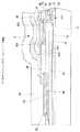
図5は、下記特許文献1に開示された有機EL表示装置100の概略構成を示す平面図である。この図において、一番外側の実線は透明のパネル基板102を示し、その中央やや上側に、上述の画素がマトリクス状に配置された破線で示す表示領域104が位置している。表示領域104の上側の辺に沿ってデータラインDLと接続される水平走査駆動回路(以下、H系ドライバと記す)106が形成され、また表示領域104の左右の辺に沿ってゲートラインGLに接続される垂直走査駆動回路(以下、V系ドライバと記す)108が形成されている。これらのドライバ106,108は、各画素ごとに設けられた薄膜トランジスタと同時に作り込まれた薄膜トランジスタなどから構成されている。 FIG. 5 is a plan view showing a schematic configuration of the organic
表示領域104内で垂直方向に延びる太い実線は、電源ラインPLを示している。個々の電源ラインPLは、表示領域104の下側の辺に沿って延びる水平方向の幅広部110につながり、全体で櫛歯形状になっている。幅広部110は更に、その中央付近で、垂直方向に延びるもう一つの幅広部112につながっている。さらに、この幅広部112は、有機EL表示装置100の下辺に配置される駆動電源入力端子T1につながっている。 A thick solid line extending in the vertical direction in the
有機EL表示装置100の下辺には、端子T1の他、カソード端子T2、V系ドライバ108につながる端子T3、H系ドライバ106につながる端子T4の複数の端子が配置される。 On the lower side of the organic
従来の有機EL表示装置の外部接続用の端子は、前記公報に記載されるように装置の下辺に設けられている。しかしながら、表示装置以外の他の機器との関連において、端子を右、または左の側辺に配置したいという要求がある。一方、表示領域104内の回路構成やドライバなどはできる限り従来の構成を踏襲することが望まれる。このため、従来の外部接続用の端子を単に側辺に移動しただけでは、これらの端子とドライバなど他の回路とを接続する配線が長くなり配線抵抗が増加し、また配線同士が近接するようになり、近接配線間の容量が増加するなどして、配線負荷が増加するという問題があった。配線負荷の増加は、消費電力の増加を招くという問題もあった。 The terminal for external connection of the conventional organic EL display device is provided on the lower side of the device as described in the publication. However, in connection with other devices other than the display device, there is a demand to arrange the terminals on the right or left side. On the other hand, it is desirable that the circuit configuration, drivers, and the like in the
本発明は、有機EL表示装置の外部接続用端子を左または右の側辺に設ける場合、各回路、各端子の配置を適正化すること、および表示装置の消費電力を抑制すること、の少なくとも一つを目的とする。 In the present invention, when the external connection terminal of the organic EL display device is provided on the left or right side, at least the arrangement of each circuit and each terminal and the power consumption of the display device are suppressed. One purpose.
本発明のエレクトロルミッネセンス表示装置は、当該表示装置の外部接続端子が、表示装置の側辺に配列され、この外部接続端子は、水平走査系配線用の端子、カソード電源用の端子、が測道電源用の端子を含み、これらの端子の配列順は、表示装置における上側から順に、水平走査系配線用の端子、カソード電源用の端子、画素駆動電源用の端子、の順で配列されている。 In the electroluminescence display device of the present invention, the external connection terminals of the display device are arranged on the side of the display device, and the external connection terminals include a horizontal scanning system wiring terminal, a cathode power supply terminal, Includes the terminals for the roadway power supply, and the arrangement order of these terminals is arranged in the order of the horizontal scanning system wiring terminal, the cathode power supply terminal, and the pixel drive power supply terminal from the upper side in the display device. Has been.
また、本発明の他の態様によるエレクトロルミッネセンス表示装置は、当該表示装置の外部接続端子が、表示装置の側辺に配列され、この外部接続端子は、表示装置における上側から順に、垂直走査系配線用の端子、水平走査系配線用の端子、カソード電源用の端子、画素駆動電源用の端子、の順で配列されている。 Further, in the electroluminescence display device according to another aspect of the present invention, the external connection terminals of the display device are arranged on the side of the display device, and the external connection terminals are vertically arranged in order from the upper side of the display device. The scanning system wiring terminals, the horizontal scanning system wiring terminals, the cathode power supply terminals, and the pixel drive power supply terminals are arranged in this order.
さらに、当該表示装置の表示領域の上辺に隣接して水平走査駆動回路を、表示領域の外部接続端子が配置された側辺に隣接してカソード電源接続部を、表示領域のもう一つの側辺に隣接して垂直走査駆動回路を、表示領域の下辺に隣接して画素駆動電源用配線を配置することができる。 Further, the horizontal scanning drive circuit is adjacent to the upper side of the display area of the display device, the cathode power supply connection is adjacent to the side of the display area where the external connection terminals are arranged, and the other side of the display area. A vertical scanning drive circuit can be arranged adjacent to the pixel, and a pixel drive power supply wiring can be arranged adjacent to the lower side of the display area.
さらに、前記配列された外部接続端子群の中心を、当該表示装置の表示領域の、水平方向に延びる中心線より下に配置することができる。 Furthermore, the centers of the arranged external connection terminal groups can be arranged below the center line extending in the horizontal direction in the display area of the display device.
さらに、前記垂直走査駆動回路の、クロック信号およびスタート信号の少なくとも一方の振幅を増加させるレベルシフタを、当該垂直走査駆動回路が配置された表示領域側辺の、これと前記振幅を増加させる信号の配線が配置された辺とが交差する端に配置することができる。 Further, a level shifter for increasing the amplitude of at least one of the clock signal and the start signal of the vertical scanning driving circuit is arranged on the side of the display area where the vertical scanning driving circuit is arranged and the signal wiring for increasing the amplitude Can be placed at the end where the side where the is placed intersects.
外部接続端子のうち、水平走査系配線用端子、カソード電源用端子、画素駆動用電源用端子を、この順で上方から配列することで、従来のレイアウトを大きく変更することなく、配線を短いものとすることができる。配線を短いものとすることで、この部分の電力損失を抑制することができる。 Among the external connection terminals, the horizontal scanning system wiring terminal, cathode power supply terminal, and pixel drive power supply terminal are arranged from above in this order, so that the wiring can be shortened without greatly changing the conventional layout. It can be. By shortening the wiring, power loss in this portion can be suppressed.
また、外部接続端子の配列を、上方から順に垂直走査系配線用端子、水平走査系配線用端子、カソード電源用端子、画素駆動用電源用端子とすることで、従来のレイアウトを大きく変更することなく、配線を短いものとすることができる。配線を短いものとしたことで、この部分の発熱による電力損失を抑制することができる。 In addition, the layout of the external connection terminals is changed from the top to the vertical scanning system wiring terminal, horizontal scanning system wiring terminal, cathode power supply terminal, and pixel drive power supply terminal, thereby greatly changing the conventional layout. In addition, the wiring can be shortened. By shortening the wiring, power loss due to heat generation in this portion can be suppressed.
また、表示領域の上辺に隣接して水平走査駆動回路を、外部接続端子が配置された側辺に隣接してカソード電源接続部を、表示領域のもう一つの側辺に隣接して垂直走査駆動回路を、表示領域の下辺に隣接して画素駆動電源用配線が配置されていることにより、有機EL素子を表示領域の周囲で封止するための領域を有効利用することができる。すなわち、この封止のための領域の下に、前述の駆動回路等を配置してスペースの有効利用が図られる。これにより、表示領域とパネル基板の縁との間の、いわゆる額縁部分の幅を狭くすることに有利となるともに、この部分の幅を一定または近いものにし、パネル基板と表示領域の原点のずれを小さくすることに、またパネル基板の外形を小さくすることに有利となる。 Also, the horizontal scanning drive circuit is adjacent to the upper side of the display area, the cathode power supply connection is adjacent to the side where the external connection terminals are arranged, and the vertical scanning drive is adjacent to the other side of the display area. Since the pixel driving power supply wiring is arranged adjacent to the lower side of the display area, the area for sealing the organic EL element around the display area can be used effectively. That is, the above-described drive circuit and the like are disposed under the sealing region, so that the space can be effectively used. This is advantageous in reducing the width of the so-called frame portion between the display area and the edge of the panel substrate, and also makes the width of this portion constant or close, so that the origin of the panel substrate and the display area is shifted. It is advantageous to reduce the size of the panel substrate and to reduce the outer shape of the panel substrate.
以下、本発明の実施形態を、図面に従って説明する。図1は、本実施形態の有機EL表示装置10の表示部、各回路および配線などの概略配置を示す図である。パネル基板12上には、複数の画素がマトリクス状に配置されて表示領域14が形成されている。パネル基板12の表示領域14には、マトリクスの水平走査(行)方向には、順次選択信号が出力されるゲートライン16(GL)が形成され、垂直走査(列)方向には、データ信号が出力されるデータライン18(DL)と、被駆動素子である有機EL素子に動作電源(PVDD)を供給するための電源ライン20(PL)が形成されている。 Hereinafter, embodiments of the present invention will be described with reference to the drawings. FIG. 1 is a diagram showing a schematic arrangement of a display unit, circuits, wirings, and the like of the organic
各画素は、概ねこれらのラインによって規定された領域に設けられており、各画素は回路構成としては、被駆動素子として有機EL素子、nチャネル型薄膜トランジスタより構成された選択トランジスタTr1、保持容量Cs、pチャネル型薄膜トランジスタより構成された素子駆動トランジスタTr2を有する。選択トランジスタTr1は、そのドレインが垂直走査方向に並ぶ各画素にデータ電圧を供給するデータライン18に接続され、ゲートが1水平走査ライン上に並ぶ画素を選択するためのゲートライン16に接続され、更にそのソースが素子駆動トランジスタTr2のゲートに接続される。素子駆動トランジスタTr2は、そのソースが電源ライン20に接続され、ドレインが有機EL素子55のアノードに接続されている。また、有機EL素子55のカソードは、各画素共通で形成されており、カソード電源CVに接続されている。また、素子駆動トランジスタTr2のゲートおよび選択トランジスタTr1のソースには、保持容量Csの第1電極が接続され、もう一方の第2電極は一定電位に、例えば電源ライン20に接続されている。 Each pixel is generally provided in a region defined by these lines, and each pixel has a circuit configuration of an organic EL element as a driven element, a selection transistor Tr1 formed of an n-channel thin film transistor, and a storage capacitor Cs. And an element driving transistor Tr2 composed of a p-channel thin film transistor. The selection transistor Tr1 has a drain connected to a
なお、上記選択トランジスタTr1および素子駆動トランジスタTr2は、いずれも能動層に、例えばレーザアニール等によって多結晶化された多結晶シリコンなど、結晶性のシリコンが用いられ、かつ不純物としてそれぞれn導電型と、p導電型がドープされたnチャネル型、pチャネル型の薄膜トランジスタで構成することができる。 Both the selection transistor Tr1 and the element driving transistor Tr2 are made of crystalline silicon such as polycrystalline silicon that has been crystallized by laser annealing or the like in the active layer, and each has n conductivity type as an impurity. , P channel type doped n channel type and p channel type thin film transistors.
画素回路のトランジスタとして、上記のように結晶性シリコンを能動層に用いた薄膜トランジスタを採用した場合、この結晶性シリコン薄膜トランジスタは、各画素回路だけでなく、各画素を順次選択、制御するための周辺駆動回路の回路素子としても用いることができる。そこで、本実施形態の有機EL表示装置10においては、パネル基板12上に、前述の画素回路用トランジスタの製造と同時に、画素回路と同様の結晶性シリコン薄膜トランジスタを形成して、周辺駆動回路、具体的にはH系ドライバ22とV系ドライバ24を内蔵させている。図1に示されるように、H系ドライバ22は表示領域14の上辺に隣接して、V系ドライバ24は、表示領域の右辺に隣接して配置される。 When the thin film transistor using crystalline silicon as the active layer is used as the transistor of the pixel circuit as described above, this crystalline silicon thin film transistor is a peripheral for sequentially selecting and controlling each pixel as well as each pixel circuit. It can also be used as a circuit element of a driver circuit. Therefore, in the organic
さらに、表示領域14の下辺に隣接して駆動電源PVDDからの駆動電流を各画素に供給するための駆動電流配線27(図2参照)が、駆動電流配線領域26に形成される。これらH系、V系ドライバ22,24に、有機EL表示装置10の外部より制御信号、電源を供給するフレキシブル・プリンテッド・サーキット(以下、FPCと記す)28との接続端子が、パネル基板12の左辺に配置される。表示領域14の左辺に隣接して、FPCの接続端子と、H系、V系ドライバ22,24や、駆動電流配線27とを接続するための配線、また供給されたクロック信号、スタート信号の振幅をH系ドライバ22の動作に適した振幅に変換するためのH系レベルシフタ(H系LS)30(図2参照)が配置されている。なお、FPCとの接続端子は、好ましくは、表示領域の高さ方向の中央より下側に配置される。また、表示領域14の右上隅には、供給されたクロック信号、スタート信号の振幅を、V系ドライバ24の動作に適した振幅に変換するV系レベルシフタ(V系LS)32が配置される。また、カソード電源(CV)用の接点34が表示領域14の左辺に沿って配置される。 Further, a driving current wiring 27 (see FIG. 2) for supplying a driving current from the driving power supply PVDD to each pixel is formed in the driving
図2は、FPC28と接続する外部接続端子36から、H系ドライバ22、V系ドライバ24、駆動電流配線27およびカソード電源用接点34に達する配線の引き回しの様子を示す図である。外部接続端子36は、垂直走査方向において上側からV系ドライバ24に係る配線である垂直走査系配線60用の端子(以下V系端子)38、H系ドライバ22に係る配線である水平走査系配線62用の端子(以下H系端子)40、カソード(陰極)46と電源を接続するため配線64のカソード電源用端子(以下CV端子)42、各画素に駆動電流供給するための配線27,66の駆動電源用端子(以下PVDD端子)44の順で配置されている。 FIG. 2 is a diagram showing the state of the wiring routed from the
外部接続端子36が配列された左辺と反対側である右辺に配置されたV系ドライバ24に係る配線60は、上辺のH系ドライバ22の外側を回るように配置される。V系端子38を端子群の中で上に配置したことで、対辺にあるV系ドライバ24までの配線の長さを短くすることができ、また、他の配線、特にH系ドライバ22への配線との交差を避けることができる。H系端子40をV系端子38の次に配置したことにより、上辺に配置されたH系ドライバ22間での配線を短くすることができる。 The
PVDD端子44は、端子群の中で最も下側に配置されている。これにより、前述のように下辺に配置された駆動電流配線27までの配線66の長さを短くすることができる。駆動電流が流れる配線27,66における電圧降下は、各画素への電流を低下させ、輝度の低下につながる。輝度の低下は、表示品位の低下につながる。また、輝度を確保しようとすれば、消費電力が増加する。このように、駆動電流が流れる配線27,66における電圧降下は、極力抑えることが好ましい。PVDD端子44を端子群の中で最も下に配置したことにより、特に配線66の長さを短くし、電圧降下を抑制することができる。さらに、PVDD端子44が、端子群の最も下に位置するだけでなく、表示領域14に対してなるべく下に、すなわち下辺になるべく近く位置することが好ましい。そのために、PVDD端子44が、表示領域14の水平方向に延びる中心線50より下に配置することが好ましく、さらには、外部接続端子36の群の中心線48(図1参照)が、表示領域の中心線50より下に配置することも好ましい。駆動電流が流れる配線27,66における電圧降下は、表示品位の劣化に直接結びつくので、H系、V系ドライバ22,24の配線の長さが多少伸びたとしても、駆動電流にかかる配線66の長さを短縮することが望ましく、そのためには、前述のように外部接続端子群を下方に配置することが好適である。CV端子42は、H系端子40とPVDD端子44の間に設けられる。 The
見方を変えれば、まず外部接続端子36に最も近い辺である左辺に配置されるカソード電源用接点34に関連するCV端子42が内側に配置され、その外側に上辺に配置されるH系ドライバ22に関連するH系端子40と下辺に駆動電流配線27に関連するPVDD端子44が配置される。更に、その外側に、外部接続端子36の配置された左辺に対向する辺、すなわち左辺より最も遠くの辺である右辺に配置されたV系ドライバ24に関連するV系端子38が配置される。駆動電流配線27は、配線負荷を小さくするために、なるべく広い幅を確保したいという要望があり、V系ドライバ24への配線は上辺に配置することが好ましい。このため、V系端子38は、H系端子40とPVDD端子44の内、H系端子40の外側すなわち上方に配置される。 In other words, first, the
図3は、図2のA−A線における断面図であり、CV端子42からカソード(陰極)46に至る配線64周辺の断面を示す図である。ガラスまたはプラスチック等の透明材料からなるパネル基板12上には、例えば、シリコン窒化(SiN)膜と、シリコン酸化(SiO2)膜が、基板側からこの順に形成された多層構造のバッファ層70が化学気相成長法(CVD)などにより形成されている。バッファ層70上には、CVDなどで成膜した非晶質(アモルファス)シリコンをレーザアニール等により得た多結晶シリコンなどの結晶性シリコン層が形成される。この結晶性シリコン層は所望形状にパターニングされ、薄膜トランジスタ(TFT)の能動層72や、必要に応じて図示しない電極や配線の一部として利用される。結晶性シリコン層のパターニング後、この結晶性シリコン層を含む基板の全面を覆うようにゲート絶縁層74を成膜する。ゲート絶縁層74は、例えば、結晶性シリコン層側からSiO2膜とSiN膜が積層された多層構造を有する。ゲート絶縁層74の上には、次にCr等の高融点金属層を形成し、この金属層をパターニングし、TFTの形成領域、つまり能動層72の形成領域ではそのチャネル領域を形成すべき領域に選択的に残しゲート電極76を得る。なお、この金属層は、各画素に選択信号を供給するための選択ライン(ゲートライン)としても用いることができ、その場合、TFTのゲート電極76の形成と同時にパネルの水平走査方向に延びる所望配線形状に金属層を選択的に残すことで得ることができる。ゲート電極76の形成後、ゲート電極76をマスクとしてTFTの導電型に応じてリン又はボロン等の不純物が能動層72にドープされる。能動層72のゲート電極の下部には不純物のドープされず真性のチャネル領域が形成され、チャネル領域の両側でゲート電極に上方が覆われていない領域には不純物がドープされてドレイン領域、ソース領域が形成される。FIG. 3 is a cross-sectional view taken along the line AA in FIG. 2 and shows a cross section around the
不純物の注入後、ゲート絶縁層74およびゲート電極76を覆う基板全面には層間絶縁層78が形成され、この層間絶縁層78は、例えば、ゲート絶縁層74側からSiN膜、SiO2膜がこの順で積層された多層構造を備える。After the impurity implantation, an
層間絶縁層78とゲート絶縁層74を貫通するように、能動層72のソース領域及びドレイン領域が露出するようにコンタクトホールが形成され、このコンタクトホールにおいて層間絶縁層78の上に形成されたドレイン電極80、ソース電極82と、能動層72の対応するドレイン領域、ソース領域とが接続される。ドレイン電極80およびソース電極82は、例えば、能動層72との接触界面側からMo(モリブデン)、Al(アルミニウム)、Moが順に積層され得られた積層構造の金属層をパターニングして構成されている。このMo/Al/Moの金属層は、他の配線84としても用いられ、ドレイン電極80及びソース電極82の形成と同時に形成パターニングして得られる。例えば、この金属層は、図示しない各画素にデータ信号を供給するデータラインDLや、電源PVDDからの電流を有機EL素子に供給するための電源ラインとしても用いられる。さらに、図3の左端に示すように、パネルと外部回路とを接続するための端子(図3では、CV端子42を表している)としても用いられ、端子形状にパターニングされている。 A contact hole is formed so as to expose the source region and the drain region of the
積層構造の金属層を形成パターニングしてドレイン、ソース電極80,82及び配線84、端子を形成した後、この金属層及び層間絶縁層78を覆う基板全面にはアクリル系樹脂などの有機絶縁材料や、他の無機材料などを用いて第1平坦化絶縁層86が例えばスピンコート及びその後の焼成を経て形成されている。 After forming a metal layer having a laminated structure and patterning to form drains,
第1平坦化絶縁層86には、例えばドレイン電極80(又はソース電極82)の対応領域、上記端子形成領域においてコンタクトホールが形成され、その後、第1平坦化絶縁層86上には、ITO(Indium Tin Oxide)や、IZO(Indium Zinc Oxide)などの導電性透明金属酸化層をスパッタリングなどによって形成し、所望形状にパターニングする。ドレイン又はソース電極80、82の対応領域では、透明導電性金属酸化物層は、透明画素電極88として用いられ、第1平坦化絶縁層86に形成されたコンタクトホールを介してドレイン電極80(又はソース電極82)と接続される。本実施形態では、この透明画素電極88は、有機EL素子55の第1電極(陽極)88として用いている。また、この透明画素電極88の形成と同時に、端子形成領域において第1平坦化絶縁層86を除去して露出させた上記Mo/Al/Moの金属端子層の上にも透明導電性金属酸化物層を選択的に残す。このように、端子の電気的特性としては、Alを含む積層構造の上記金属端子層を用いれば十分であるが、この金属端子層表面を導電性の金属酸化層で覆う構成とすることで、本実施形態では、金属端子表面が外界雰囲気に曝され、大気中の酸素、水などによる表面酸化によって接続抵抗が増大することを防止できる。 In the first
また、端子部分だけでなく端子から延びる配線領域も必要に応じて導電性金属酸化層で覆うことにより、大気中の酸素や水分が、この配線を通じ(例えば配線表面を酸化させながら)、後に封止パネルを接着することで封止する有機EL素子の形成された表示領域内に侵入することを防止できる。 Further, not only the terminal portion but also the wiring region extending from the terminal is covered with a conductive metal oxide layer as necessary, so that oxygen and moisture in the atmosphere can be sealed later through this wiring (for example, oxidizing the wiring surface). By adhering the stop panel, it is possible to prevent intrusion into the display area where the organic EL element to be sealed is formed.
導電性金属酸化層を所望の位置に形成した後、基板全体を覆うように第1平坦化絶縁層86と同様にアクリル系樹脂などを用いて第2平坦化絶縁層90が形成される。第2平坦化絶縁層90は、前述の第1電極88の形成領域ではそのエッジ部分を除いて開口されている。エッジ部分を覆うのは該エッジ部分で、第1電極88と後述する有機EL素子の第2電極46とが間に形成された後述する発光素子層92の被覆性が低下し、あるいは電界集中が発生して短絡することを防止するためである。 After the conductive metal oxide layer is formed at a desired position, the second
発光素子層92は、少なくとも発光機能を備える有機化合物を含む発光層を備えるが、用いる化合物の機能などにより、単層構造でも多層構造でもよい。本実施形態のように第1電極88が陽極、第2電極46が陰極の場合において、一例として、第1電極側から正孔注入層921、正孔輸送層922、発光層923、電子輸送層924などの積層構造を有する。また発光素子層92は、低分子系有機化合物を材料に用いている場合、真空蒸着法によって各層を形成することができるが、高分子系有機化合物を用いた場合などはインクジェット印刷法や、スピンコートなどによって形成することも可能である。 The light-emitting
なお、発光層以外の電荷輸送層や、注入層は、全画素共通で形成することができる(用いる材料によって各画素で個別パターンとする必要がある場合もある)。また、各画素のEL素子の発光色が白色で、カラーフィルタを用いてR,G,Bの光を得てフルカラー表示を行う場合には、有機EL素子の発光層は、真空蒸着によって形成する場合にもマスクによる個別パターンの形成は不要であり、他の有機層と同様に、全画素共通で成膜できる。各画素のEL素子が対応するR,G,Bの光を発光する場合には、発光色毎に異なる有機発光材料を用いる必要があり、少なくとも、画素毎に個別パターンで発光層を形成する。 Note that the charge transport layer and the injection layer other than the light-emitting layer can be formed in common for all pixels (there may be an individual pattern for each pixel depending on the material used). In addition, when the light emission color of the EL element of each pixel is white and R, G, B light is obtained using a color filter and full color display is performed, the light emitting layer of the organic EL element is formed by vacuum deposition. Even in this case, it is not necessary to form an individual pattern using a mask, and the film can be formed in common for all pixels as in the case of other organic layers. When the EL element of each pixel emits corresponding R, G, and B light, it is necessary to use different organic light emitting materials for each emission color, and at least a light emitting layer is formed in an individual pattern for each pixel.
発光素子層92の上には、これを覆うように各画素共通でAlや、Al合金、MgAg合金等を用いた第2電極46が真空蒸着法などによって形成されている。上述のように、なお、本実施形態では、この第2電極46は、陰極(カソード電極)として機能している。また、カソード電極46は、表示領域14の水平走査方向の端、この実施形態においては、左辺においてCV端子から延びる配線64と接続されている。なお、配線64の少なくとも上部層が、上述のように透明画素電極88と同層の透明導電性金属酸化層で構成されている場合、この配線64とカソード電極46との接続は、表示領域外では、通常第2平坦化絶縁層90は除去され、また発光素子層92も積層されていないため、最上層に露出している透明導電性金属酸化物層64の上に直接カソード電極46が形成されることで達成される。なお、カソード電極46と配線64との接続部において、配線64の上部層として透明導電性金属酸化層を用いておらず、Mo/Al/Mo金属層のみが形成されている場合、層間絶縁層78、第1平坦化絶縁層86には開口部が形成され、この開口部の底面に露出したMo/Al/Mo金属層を覆うようにカソード電極46が積層されて電気的に接続される。全面形成されたカソード電極46のさらに上には、基板全面を覆うようにスパッタなどによってSiN等の保護層94が形成されている。 On the light emitting
以上のように、本実施形態によれば、PVDD端子44を表示領域の水平方向に延びる中心線より下に配置したことにより駆動電流にかかる配線を短くし、抵抗を小さくして、消費電力や表示品位の低下を抑えることができる。また、V系ドライバ24に係る配線を上辺に配置することにより、表示領域14の縁と、当該表示装置の外形となるパネル基板12の縁の間である額縁の幅を、駆動電流配線の幅を確保しつつ、上下で近づけることができ、すなわち、表示中心のYアドレスとパネル基板のガラス外形中心のYアドレスを一致させることが可能となり、様々な機器に対する取り付け自由度が向上する。V系ドライバ24は、左辺に配置することも可能であるが、この場合、カソード46との間に寄生容量が発生し、消費電力が増加する可能性がある。また、右辺においても有機EL層等を封止する必要があり、このためのスペースが存在し、ここにV系ドライバ24を配置すれば、スペースの有効利用を図ることができる。 As described above, according to the present embodiment, by arranging the
以上の配置によって、封止上必要な額縁スペースにバランスよく各回路と各配線を配置できガラス基板の有効活用が可能となり、表示品質の向上、低消費電力化、およびコスト低下が実現できる。 With the above arrangement, each circuit and each wiring can be arranged in a well-balanced frame space necessary for sealing, and the glass substrate can be effectively used. Thus, display quality can be improved, power consumption can be reduced, and cost can be reduced.
以上の実施形態においては、外部接続端子を表示装置の左辺に配置した場合を説明したが、右辺に配置することもできる。その場合、各回路、配線等の配置も左右対称となる。 Although the case where the external connection terminal is arranged on the left side of the display device has been described in the above embodiment, it can be arranged on the right side. In that case, the arrangement of each circuit, wiring and the like is also symmetrical.
10 有機EL表示装置、12 パネル基板、14 表示領域、22 H系ドライバ、24 V系ドライバ、27 駆動電流配線、28 フレキシブル・プリンテッド・サーキット(FPC)、30 H系レベルシフタ、32 V系レベルシフタ、34 カソード電源用接点、36 外部接続用端子、38 垂直走査系配線用の端子(V系端子)、40 水平走査系配線用の端子(H系端子)、42 カソード電源用の端子(CV端子)、44 駆動電源用の端子(PVDD端子)、48 外部接続端子の中心線、50 表示領域の中心線、55 有機EL素子。 10 organic EL display device, 12 panel substrate, 14 display area, 22 H system driver, 24 V system driver, 27 drive current wiring, 28 flexible printed circuit (FPC), 30 H system level shifter, 32 V system level shifter, 34 Cathode power contact, 36 External connection terminal, 38 Vertical scanning system wiring terminal (V system terminal), 40 Horizontal scanning system wiring terminal (H system terminal), 42 Cathode power supply terminal (CV terminal) , 44 Terminal for driving power supply (PVDD terminal), 48 Center line of external connection terminal, 50 Center line of display area, 55 Organic EL element.
Claims (5)
Translated fromJapanese当該表示装置の外部接続端子は、表示装置の側辺に配列され、
前記外部接続端子は、水平走査系配線用の端子、カソード電源用の端子、画素駆動電源用の端子を含み、これらの端子の配列順は、表示装置における上側から順に、水平走査系配線用の端子、カソード電源用の端子、画素駆動電源用の端子、の順である、
エレクトロルミネッセンス表示装置。In an electroluminescence display device having a display portion in which pixels are arranged in a matrix,
The external connection terminals of the display device are arranged on the side of the display device,
The external connection terminals include a terminal for horizontal scanning system wiring, a terminal for cathode power supply, and a terminal for pixel drive power supply. The arrangement order of these terminals is for horizontal scanning system wiring in order from the upper side in the display device. Terminal, cathode power supply terminal, pixel drive power supply terminal, in that order.
Electroluminescence display device.
前記外部接続端子は、表示装置における上側から順に、垂直走査系配線用の端子、水平走査系配線用の端子、カソード電源用の端子、画素駆動電源用の端子、の順で配列されている、
エレクトロルミネッセンス表示装置。The electroluminescent display device according to claim 1,
The external connection terminals are arranged in the order of the vertical scanning system wiring terminal, the horizontal scanning system wiring terminal, the cathode power supply terminal, and the pixel drive power supply terminal from the upper side in the display device.
Electroluminescence display device.
当該表示装置の表示領域の上辺に隣接して水平走査駆動回路が、表示領域の外部接続端子が配置された側辺に隣接してカソード電源接続部が、表示領域のもう一つの側辺に隣接して垂直走査駆動回路が、表示領域の下辺に隣接して画素駆動電源用配線が配置されている、
エレクトロルミネッセンス表示装置。The electroluminescence display device according to claim 1 or 2,
The horizontal scanning drive circuit is adjacent to the upper side of the display area of the display device, the cathode power supply connection is adjacent to the other side of the display area, adjacent to the side of the display area where the external connection terminals are arranged. In the vertical scanning drive circuit, pixel drive power supply wiring is disposed adjacent to the lower side of the display area.
Electroluminescence display device.
前記配列された外部接続端子の群の中心が、当該表示装置の表示領域の、水平方向に延びる中心線より下に配置される、
エレクトロルミネッセンス表示装置。The electroluminescent display device according to claim 3.
The center of the group of the external connection terminals arranged is arranged below the center line extending in the horizontal direction of the display area of the display device.
Electroluminescence display device.
前記垂直走査駆動回路の、クロック信号およびスタート信号の少なくとも一方の振幅を増加させるレベルシフタが、当該垂直走査駆動回路が配置された表示領域側辺の、この側辺と前記振幅を増加させる信号の配線が配置された辺とが交差する端に配置されている、
エレクトロルミネッセンス表示装置。The electroluminescence display device according to claim 3 or 4,
The level shifter for increasing the amplitude of at least one of the clock signal and the start signal of the vertical scanning driving circuit is arranged on the side of the display area where the vertical scanning driving circuit is arranged and the wiring of the signal for increasing the amplitude Is located at the end where the side where
Electroluminescence display device.
Priority Applications (5)
| Application Number | Priority Date | Filing Date | Title |
|---|---|---|---|
| JP2005202992AJP2007026703A (en) | 2005-07-12 | 2005-07-12 | Electroluminescent display device |
| TW095122428ATW200703216A (en) | 2005-07-12 | 2006-06-22 | Electroluminescense display device |
| KR1020060064986AKR100778619B1 (en) | 2005-07-12 | 2006-07-11 | Electroluminescence display |
| US11/485,526US7742023B2 (en) | 2005-07-12 | 2006-07-12 | Electroluminescence display device |
| CNB2006101018915ACN100539777C (en) | 2005-07-12 | 2006-07-12 | El display device |
Applications Claiming Priority (1)
| Application Number | Priority Date | Filing Date | Title |
|---|---|---|---|
| JP2005202992AJP2007026703A (en) | 2005-07-12 | 2005-07-12 | Electroluminescent display device |
Publications (1)
| Publication Number | Publication Date |
|---|---|
| JP2007026703Atrue JP2007026703A (en) | 2007-02-01 |
Family
ID=37610091
Family Applications (1)
| Application Number | Title | Priority Date | Filing Date |
|---|---|---|---|
| JP2005202992APendingJP2007026703A (en) | 2005-07-12 | 2005-07-12 | Electroluminescent display device |
Country Status (2)
| Country | Link |
|---|---|
| JP (1) | JP2007026703A (en) |
| CN (1) | CN100539777C (en) |
Cited By (2)
| Publication number | Priority date | Publication date | Assignee | Title |
|---|---|---|---|---|
| JP2009099777A (en)* | 2007-10-17 | 2009-05-07 | Sony Corp | Display devices and electronic devices |
| JP2020021734A (en)* | 2005-08-31 | 2020-02-06 | 株式会社半導体エネルギー研究所 | Light-emitting device |
Families Citing this family (3)
| Publication number | Priority date | Publication date | Assignee | Title |
|---|---|---|---|---|
| US20130168147A1 (en)* | 2010-10-08 | 2013-07-04 | Yasuhiro Kohara | Electronic device |
| CN114256287A (en)* | 2021-12-22 | 2022-03-29 | Tcl华星光电技术有限公司 | Display panel and display device |
| CN114220825B (en)* | 2022-02-22 | 2022-08-23 | 上海天马微电子有限公司 | Light-emitting drive substrate, light-emitting panel and display device |
Citations (4)
| Publication number | Priority date | Publication date | Assignee | Title |
|---|---|---|---|---|
| JP2000357584A (en)* | 1999-06-14 | 2000-12-26 | Seiko Epson Corp | Circuit board for light emitting element, electronic device and display device |
| JP2001242827A (en)* | 1999-12-24 | 2001-09-07 | Semiconductor Energy Lab Co Ltd | Electronic equipment |
| JP2003280548A (en)* | 2002-03-25 | 2003-10-02 | Toshiba Corp | Flexible display panel |
| JP2003344873A (en)* | 2002-05-24 | 2003-12-03 | Toshiba Corp | Bootstrap circuit, flat panel display using the same |
- 2005
- 2005-07-12JPJP2005202992Apatent/JP2007026703A/enactivePending
- 2006
- 2006-07-12CNCNB2006101018915Apatent/CN100539777C/enactiveActive
Patent Citations (4)
| Publication number | Priority date | Publication date | Assignee | Title |
|---|---|---|---|---|
| JP2000357584A (en)* | 1999-06-14 | 2000-12-26 | Seiko Epson Corp | Circuit board for light emitting element, electronic device and display device |
| JP2001242827A (en)* | 1999-12-24 | 2001-09-07 | Semiconductor Energy Lab Co Ltd | Electronic equipment |
| JP2003280548A (en)* | 2002-03-25 | 2003-10-02 | Toshiba Corp | Flexible display panel |
| JP2003344873A (en)* | 2002-05-24 | 2003-12-03 | Toshiba Corp | Bootstrap circuit, flat panel display using the same |
Cited By (2)
| Publication number | Priority date | Publication date | Assignee | Title |
|---|---|---|---|---|
| JP2020021734A (en)* | 2005-08-31 | 2020-02-06 | 株式会社半導体エネルギー研究所 | Light-emitting device |
| JP2009099777A (en)* | 2007-10-17 | 2009-05-07 | Sony Corp | Display devices and electronic devices |
Also Published As
| Publication number | Publication date |
|---|---|
| CN100539777C (en) | 2009-09-09 |
| CN1897774A (en) | 2007-01-17 |
Similar Documents
| Publication | Publication Date | Title |
|---|---|---|
| JP6691190B2 (en) | Light emitting device | |
| US7742023B2 (en) | Electroluminescence display device | |
| JP2007128049A (en) | Display panel | |
| JP3922374B2 (en) | Electro-optical device, matrix substrate, and electronic apparatus | |
| KR100804859B1 (en) | Display and Array Boards | |
| JP2018097361A (en) | Organic light-emitting display device and method for manufacturing the same | |
| KR102769670B1 (en) | Organic light emitting diode display device | |
| US11563067B2 (en) | Display device with improved aperture ratio and transmissivity | |
| TWI386105B (en) | Display panel | |
| JP6872343B2 (en) | Display device and manufacturing method of display device | |
| US9190461B2 (en) | Organic light-emitting display device | |
| JP5724105B2 (en) | Thin film transistor array device, EL display panel, EL display device, thin film transistor array device manufacturing method, and EL display panel manufacturing method | |
| KR20200093718A (en) | Organic light emitting diode display device and method of manufacturing organic light emitting diode display device | |
| JP2008123986A (en) | Organic electroluminescence display | |
| JP6334979B2 (en) | Display device, display device manufacturing method, and electronic apparatus | |
| KR20200087368A (en) | Organic light emitting diode display device | |
| JP2009200336A (en) | Self-luminous type display | |
| JP4287337B2 (en) | Organic electroluminescent display device and manufacturing method thereof | |
| JP4755142B2 (en) | LIGHT EMITTING DEVICE AND ELECTRONIC DEVICE USING LIGHT EMITTING DEVICE | |
| JP2007026703A (en) | Electroluminescent display device | |
| US20220199955A1 (en) | Display device and manufactring method thereof | |
| JP2007026704A (en) | Electroluminescent display device | |
| CN1945848A (en) | Display panel | |
| KR100684825B1 (en) | Organic electroluminescence display device and manufacturing method thereof | |
| JP2007047329A (en) | Electroluminescence display panel |
Legal Events
| Date | Code | Title | Description |
|---|---|---|---|
| A621 | Written request for application examination | Free format text:JAPANESE INTERMEDIATE CODE: A621 Effective date:20080711 | |
| A977 | Report on retrieval | Free format text:JAPANESE INTERMEDIATE CODE: A971007 Effective date:20101005 | |
| A131 | Notification of reasons for refusal | Free format text:JAPANESE INTERMEDIATE CODE: A131 Effective date:20101130 | |
| A521 | Request for written amendment filed | Free format text:JAPANESE INTERMEDIATE CODE: A523 Effective date:20110131 | |
| A02 | Decision of refusal | Free format text:JAPANESE INTERMEDIATE CODE: A02 Effective date:20110621 |