JP2007019107A - Semiconductor device and its manufacturing method - Google Patents
Semiconductor device and its manufacturing methodDownload PDFInfo
- Publication number
- JP2007019107A JP2007019107AJP2005196672AJP2005196672AJP2007019107AJP 2007019107 AJP2007019107 AJP 2007019107AJP 2005196672 AJP2005196672 AJP 2005196672AJP 2005196672 AJP2005196672 AJP 2005196672AJP 2007019107 AJP2007019107 AJP 2007019107A
- Authority
- JP
- Japan
- Prior art keywords
- semiconductor device
- substrate
- organic material
- sealing structure
- sealing
- Prior art date
- Legal status (The legal status is an assumption and is not a legal conclusion. Google has not performed a legal analysis and makes no representation as to the accuracy of the status listed.)
- Pending
Links
- 239000004065semiconductorSubstances0.000titleclaimsabstractdescription84
- 238000004519manufacturing processMethods0.000titleclaimsabstractdescription42
- 238000007789sealingMethods0.000claimsabstractdescription74
- 239000000758substrateSubstances0.000claimsabstractdescription61
- 239000011368organic materialSubstances0.000claimsabstractdescription40
- 229910010272inorganic materialInorganic materials0.000claimsdescription36
- 239000011147inorganic materialSubstances0.000claimsdescription36
- 230000001681protective effectEffects0.000claimsdescription35
- 238000000034methodMethods0.000claimsdescription30
- 239000000853adhesiveSubstances0.000claimsdescription9
- 230000001070adhesive effectEffects0.000claimsdescription9
- 230000003287optical effectEffects0.000claimsdescription8
- 230000005540biological transmissionEffects0.000claimsdescription6
- 238000010586diagramMethods0.000description17
- 239000011347resinSubstances0.000description14
- 229920005989resinPolymers0.000description14
- 239000000463materialSubstances0.000description13
- 239000012790adhesive layerSubstances0.000description12
- XUIMIQQOPSSXEZ-UHFFFAOYSA-NSiliconChemical compound[Si]XUIMIQQOPSSXEZ-UHFFFAOYSA-N0.000description10
- 229910052710siliconInorganic materials0.000description10
- 239000010703siliconSubstances0.000description10
- 239000007789gasSubstances0.000description9
- 230000035699permeabilityEffects0.000description6
- 238000005520cutting processMethods0.000description5
- 230000000694effectsEffects0.000description5
- 239000007769metal materialSubstances0.000description4
- 229910001218Gallium arsenideInorganic materials0.000description3
- -1Si 3 N 4Inorganic materials0.000description2
- 229910004298SiO 2Inorganic materials0.000description2
- 238000006243chemical reactionMethods0.000description2
- 238000005229chemical vapour depositionMethods0.000description2
- 239000000428dustSubstances0.000description2
- 239000011261inert gasSubstances0.000description2
- 238000005304joiningMethods0.000description2
- 239000010410layerSubstances0.000description2
- 229910052814silicon oxideInorganic materials0.000description2
- 238000004544sputter depositionMethods0.000description2
- NIPNSKYNPDTRPC-UHFFFAOYSA-NN-[2-oxo-2-(2,4,6,7-tetrahydrotriazolo[4,5-c]pyridin-5-yl)ethyl]-2-[[3-(trifluoromethoxy)phenyl]methylamino]pyrimidine-5-carboxamideChemical compoundO=C(CNC(=O)C=1C=NC(=NC=1)NCC1=CC(=CC=C1)OC(F)(F)F)N1CC2=C(CC1)NN=N2NIPNSKYNPDTRPC-UHFFFAOYSA-N0.000description1
- 230000001133accelerationEffects0.000description1
- 230000015572biosynthetic processEffects0.000description1
- 239000011247coating layerSubstances0.000description1
- 238000005530etchingMethods0.000description1
- 239000011521glassSubstances0.000description1
- 238000012986modificationMethods0.000description1
- 230000004048modificationEffects0.000description1
- 238000000465mouldingMethods0.000description1
- 238000005240physical vapour depositionMethods0.000description1
- 239000011241protective layerSubstances0.000description1
- XLYOFNOQVPJJNP-UHFFFAOYSA-NwaterSubstancesOXLYOFNOQVPJJNP-UHFFFAOYSA-N0.000description1
Images


Classifications
- B—PERFORMING OPERATIONS; TRANSPORTING
- B81—MICROSTRUCTURAL TECHNOLOGY
- B81B—MICROSTRUCTURAL DEVICES OR SYSTEMS, e.g. MICROMECHANICAL DEVICES
- B81B7/00—Microstructural systems; Auxiliary parts of microstructural devices or systems
- B81B7/0032—Packages or encapsulation
- B81B7/0035—Packages or encapsulation for maintaining a controlled atmosphere inside of the chamber containing the MEMS
- B81B7/0041—Packages or encapsulation for maintaining a controlled atmosphere inside of the chamber containing the MEMS maintaining a controlled atmosphere with techniques not provided for in B81B7/0038
- B—PERFORMING OPERATIONS; TRANSPORTING
- B81—MICROSTRUCTURAL TECHNOLOGY
- B81C—PROCESSES OR APPARATUS SPECIALLY ADAPTED FOR THE MANUFACTURE OR TREATMENT OF MICROSTRUCTURAL DEVICES OR SYSTEMS
- B81C2203/00—Forming microstructural systems
- B81C2203/01—Packaging MEMS
- B81C2203/0109—Bonding an individual cap on the substrate
- B—PERFORMING OPERATIONS; TRANSPORTING
- B81—MICROSTRUCTURAL TECHNOLOGY
- B81C—PROCESSES OR APPARATUS SPECIALLY ADAPTED FOR THE MANUFACTURE OR TREATMENT OF MICROSTRUCTURAL DEVICES OR SYSTEMS
- B81C2203/00—Forming microstructural systems
- B81C2203/01—Packaging MEMS
- B81C2203/0136—Growing or depositing of a covering layer
- H—ELECTRICITY
- H01—ELECTRIC ELEMENTS
- H01L—SEMICONDUCTOR DEVICES NOT COVERED BY CLASS H10
- H01L2924/00—Indexing scheme for arrangements or methods for connecting or disconnecting semiconductor or solid-state bodies as covered by H01L24/00
- H01L2924/15—Details of package parts other than the semiconductor or other solid state devices to be connected
- H01L2924/161—Cap
- H01L2924/1615—Shape
- H01L2924/16152—Cap comprising a cavity for hosting the device, e.g. U-shaped cap
- H—ELECTRICITY
- H01—ELECTRIC ELEMENTS
- H01L—SEMICONDUCTOR DEVICES NOT COVERED BY CLASS H10
- H01L2924/00—Indexing scheme for arrangements or methods for connecting or disconnecting semiconductor or solid-state bodies as covered by H01L24/00
- H01L2924/15—Details of package parts other than the semiconductor or other solid state devices to be connected
- H01L2924/161—Cap
- H01L2924/1615—Shape
- H01L2924/16195—Flat cap [not enclosing an internal cavity]
Landscapes
- Engineering & Computer Science (AREA)
- Microelectronics & Electronic Packaging (AREA)
- Computer Hardware Design (AREA)
- Micromachines (AREA)
Abstract
Description
Translated fromJapanese本発明は半導体装置およびその製造方法に係り、特に封止構造体を有する半導体装置およびその製造方法に関する。 The present invention relates to a semiconductor device and a manufacturing method thereof, and more particularly to a semiconductor device having a sealing structure and a manufacturing method thereof.
基板上に形成される、または基板上に搭載される素子には、様々な種類のものが存在するが、当該素子の種類によっては、基板上で封止された状態で用いられることが好ましい場合がある。 There are various types of elements formed on or mounted on a substrate, but depending on the type of the element, it is preferable to be used in a state of being sealed on the substrate There is.
例えば、マイクロ・エレクトロ・メカニカル・システム(Micro Electro Mechanical System、MEMSと呼ばれる場合がある)を用いた素子(以下文中MEMS素子)は、構造上基板上で封止されて用いられることが好ましい代表的な素子である。 For example, an element using a micro electro mechanical system (sometimes referred to as MEMS) (hereinafter referred to as a MEMS element) is preferably used by being sealed on a substrate in terms of structure. Element.
このようなMEMS素子としては、例えば圧力センサ、加速度センサ、光機能素子などがある。このようなMEMS素子は、真空状態や減圧状態、または不活性ガスで置換された雰囲気で用いられることが好ましく、素子は気密封止されて用いられることが好ましい。 Examples of such a MEMS element include a pressure sensor, an acceleration sensor, and an optical functional element. Such a MEMS element is preferably used in a vacuum state, a reduced pressure state, or an atmosphere substituted with an inert gas, and the element is preferably hermetically sealed.
このため、MEMS素子を封止する方法が様々に提案されていた(特許文献1、特許文献2参照)。例えば、樹脂材料による耐湿コーティング層を半導体素子の周囲に形成する方法や、シリコンウェハを張り合わせることにより、半導体素子を封止する方法が提案されていた。
しかし、例えば樹脂材料により素子を封止しようとした場合、樹脂材料では気体の透過率が大きく、素子を気密封止することが困難であった。このため、封止による素子の保護の効果が十分に得られない場合が生じていた。 However, for example, when an element is to be sealed with a resin material, the resin material has a large gas permeability, and it is difficult to hermetically seal the element. For this reason, the case where the effect of protection of the element by sealing cannot fully be obtained has arisen.
一方、気体の透過率が小さい無機材料を用いて素子を封止する方法としては、例えば、シリコン(シリコンウェハ)を張り合わせることにより、素子を封止する方法が提案されていた。しかし、この場合、素子を封止するためのシリコンの形状が複雑になり、シリコンの加工にコストと時間を要し、半導体装置の生産性が低下してしまう問題があった。 On the other hand, as a method for sealing an element using an inorganic material having a low gas permeability, for example, a method for sealing the element by bonding silicon (silicon wafer) has been proposed. However, in this case, there is a problem in that the shape of silicon for sealing the element becomes complicated, the cost and time are required for processing silicon, and the productivity of the semiconductor device is lowered.
そこで、本発明では、上記の問題を解決した、新規で有用な半導体装置、および半導体装置の製造方法を提供することを目的としている。 Therefore, an object of the present invention is to provide a novel and useful semiconductor device and a method for manufacturing the semiconductor device, which solve the above-described problems.
本発明の具体的な課題は、基板上で素子が封止される構造を有する半導体装置であって、単純な構造で当該素子の封止の気密性が良好となるよう構成されている半導体装置と、当該半導体装置を製造する製造方法を提供することである。 A specific problem of the present invention is a semiconductor device having a structure in which an element is sealed on a substrate, and the semiconductor device is configured to have a simple structure and good hermeticity for sealing the element. And a manufacturing method for manufacturing the semiconductor device.
本発明の第1の観点では上記の課題を、基板と、前記基板上の素子と、前記素子を封止する封止構造体と、を有し、前記封止構造体は有機材料より形成されている有機材料部を含み、該有機材料部には、無機材料よりなる保護膜が形成されていることを特徴とする半導体装置により、解決する。 According to a first aspect of the present invention, the above-described problem includes a substrate, an element on the substrate, and a sealing structure that seals the element, and the sealing structure is formed of an organic material. This is solved by a semiconductor device characterized in that a protective film made of an inorganic material is formed on the organic material portion.
当該半導体装置は、単純な構造で当該素子の封止の気密性が良好となるよう構成されている特長を有している。 The semiconductor device has a feature that the structure is simple and the airtightness of the element is good.
また、前記素子は、MEMS素子であると、MEMS素子を効果的に気密封止でき、好ましい。 The element is preferably a MEMS element because the MEMS element can be effectively hermetically sealed.
また、前記有機材料部は、一面が開口された、有機材料よりなる筐体形状を有し、該開口側が前記基板側に封止されるように設置されると、前記封止構造体を容易に形成することが可能であり、好ましい。 In addition, the organic material portion has a housing shape made of an organic material with an opening on one side, and the sealing structure can be easily formed when installed so that the opening side is sealed to the substrate side. It is possible to form it in a preferable manner.
また、前記封止構造体は、無機材料よりなる複数の無機材料部が、接着剤よりなる前記有機材料部により接合された構造であると、前記封止構造体が単純な構造の組み合わせで構成できるため、封止構造体を容易に形成することが可能となり、好ましい。 Further, the sealing structure has a structure in which a plurality of inorganic material parts made of an inorganic material are joined by the organic material part made of an adhesive, and the sealing structure is configured by a combination of simple structures. Therefore, the sealing structure can be easily formed, which is preferable.
また、前記無機材料部は、平板状の天井部と、該天井部を支持する前記基板上に設置される支持部と、を含むと、天井部と支持部を別個に形成することが可能となり、封止構造体を容易に形成することが可能となり、好ましい。 Further, when the inorganic material part includes a flat ceiling part and a support part installed on the substrate that supports the ceiling part, the ceiling part and the support part can be separately formed. The sealing structure can be easily formed, which is preferable.
また、前記素子は光機能素子であり、前記天井部の光透過面が前記保護膜から露出していると、当該天井部の光の透過特性が良好となり、光機能素子の特性を劣化させずに用いることが可能となる。 Further, the element is an optical functional element, and if the light transmission surface of the ceiling part is exposed from the protective film, the light transmission characteristic of the ceiling part is improved, and the characteristics of the optical functional element are not deteriorated. It becomes possible to use for.
また、本発明の第2の観点では、上記の課題を、基板上の素子を、封止構造体により封止して半導体装置を形成する半導体装置の製造方法であって、前記基板上の前記素子を、有機材料よりなる部分を含む前記封止構造体により封止する工程と、少なくとも前記有機材料よりなる部分に無機材料よりなる保護膜を形成する工程と、を有することを特徴とする半導体装置の製造方法により、解決する。 According to a second aspect of the present invention, there is provided a method for manufacturing a semiconductor device in which the above-described problem is achieved by sealing an element on a substrate with a sealing structure to form a semiconductor device. A semiconductor comprising: a step of sealing an element with the sealing structure including a portion made of an organic material; and a step of forming a protective film made of an inorganic material at least on a portion made of the organic material. It is solved by the manufacturing method of the device.
上記の半導体装置の製造方法では、基板上で素子が封止される構造を有する半導体装置であって、当該素子の封止の気密性が良好となるよう構成されている半導体装置を、容易に形成することが可能となる。 In the above semiconductor device manufacturing method, a semiconductor device having a structure in which an element is sealed on a substrate, the semiconductor device configured so that the hermeticity of sealing of the element is good can be easily obtained. It becomes possible to form.
また、前記素子は、MEMS素子であると、MEMS素子を効果的に気密封止して保護することが可能となり、好ましい。 Further, it is preferable that the element is a MEMS element because the MEMS element can be effectively hermetically sealed and protected.
本発明によれば、基板上で素子が封止される構造を有する半導体装置であって、単純な構造で当該素子の封止の気密性が良好となるよう構成されている半導体装置と、当該半導体装置を製造する製造方法を提供することが可能となる。 According to the present invention, there is provided a semiconductor device having a structure in which an element is sealed on a substrate, the semiconductor device being configured to have a simple structure and good hermetic sealing of the element, A manufacturing method for manufacturing a semiconductor device can be provided.
本発明に係る半導体装置は、基板上の素子が封止構造体により封止されている構造を有している。この場合に前記封止構造体は有機材料より形成されている有機材料部を含み、該有機材料部には、無機材料よりなる保護膜が形成されている。 The semiconductor device according to the present invention has a structure in which elements on a substrate are sealed with a sealing structure. In this case, the sealing structure includes an organic material portion made of an organic material, and a protective film made of an inorganic material is formed on the organic material portion.
このように、本実施例よる半導体装置では、気体の透過率が小さく、気密性に優れた無機材料よりなる保護膜が前記封止構造体に形成されているため、当該封止構造体の気密性が良好となっている。 As described above, in the semiconductor device according to the present example, since the protective film made of an inorganic material having low gas permeability and excellent airtightness is formed on the sealing structure, the airtightness of the sealing structure The property is good.
また、当該保護膜により気密性が確保されるため、封止構造体を加工や成型が容易な有機材料を用いて形成することが可能となる。このため、封止構造体の加工が容易となる効果を奏する。さらに、封止構造体を、有機材料を含む構造で形成できるために、例えば複数の部品を有機材料で接合して封止構造体を形成することが可能となる。このため、封止構造体を形成する個々の部品を単純とすることが可能となり、半導体装置の製造が容易となって製造コストを低減することが可能となる効果を奏する。 Further, since the airtightness is ensured by the protective film, the sealing structure can be formed using an organic material that can be easily processed and molded. For this reason, there exists an effect which processing of a sealing structure becomes easy. Furthermore, since the sealing structure can be formed with a structure including an organic material, it is possible to form a sealing structure by bonding a plurality of components with an organic material, for example. For this reason, it is possible to simplify the individual parts forming the sealing structure, and it is possible to easily manufacture the semiconductor device and reduce the manufacturing cost.
次に、上記の半導体装置と該半導体装置の製造方法について、図面に基づき説明する。 Next, the semiconductor device and the method for manufacturing the semiconductor device will be described with reference to the drawings.
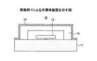
図1は、本発明の実施例1による半導体装置10を模式的に示した図である。図1を参照するに、本実施例による半導体装置10は、例えばシリコンなどの半導体よりなる基板11上に形成された、例えばMEMS素子よりなる素子12が、封止構造体13により封止された構造を有している。 FIG. 1 is a diagram schematically showing a
前記封止構造体13は、例えば樹脂材料などの有機材料よりなり、例えば一面が開口された筐体形状を有している。当該封止構造体13は、開口された側が例えば樹脂系の接着剤(図示せず)により、前記基板上に設置されて前記素子12を封止する構造になっている。 The
前記封止構造体13の外側(前記素子12に面する側の反対側)の表面から基板11上面には、無機材料よりなる保護膜14が形成されている。よって素子12を気密封止することができる。前記保護膜14は無機材料より構成されているため、気体の透過率が小さく、気密性が保たれる。このため、真空または減圧雰囲気や、不活性ガス雰囲気中で用いられることが好ましい素子、例えばMEMS素子などを気密封止することが可能となる。また、前記素子12が水分に曝される影響が抑制され、前記素子12を湿気から効果的に保護することが可能となっている。 A
例えば、従来は前記封止構造体13に相当する構造は、シリコンやガラスといった無機材料より形成される場合があったが、この場合には封止構造体に相当する構造の加工コストが高く、製造コストが高くなってしまう問題があった。また、封止構造体13に相当する構造を、例えば樹脂材料などの有機材料により形成すると、加工(成型)は容易であるが、気体の透過率が大きく、気密性が十分でない問題を有していた。 For example, conventionally, the structure corresponding to the
そこで、本実施例では、加工性が良好である有機材料、例えば樹脂材料により前記封止構造体13を形成し、該封止構造体13の表面に、気密性、耐透水性に優れた無機材料よりなる保護膜14を形成している。このため、単純な構造であって形成が容易であると共に、前記素子12の気密性が良好であり、封止による保護効果が良好である半導体装置を提供することが可能となっている。この場合、気密性が良好であると、例えば水分を含んだ気体(空気)の透過量が小さく、素子を湿気から保護する効果も奏する。 Therefore, in this embodiment, the
例えば、前記保護膜14を構成する無機材料としては、例えば金属材料としては、Ti、Ni、Cr、Arなど、非金属材料としては、SiN,SiON,Si3N4,SiO2、などの材料を用いることが可能である。また、前記保護膜14は、例えば、CVD法、PVD法(例えばスパッタ法など)により、形成することが可能である。For example, as the inorganic material constituting the
また、前記基板11は、配線基板であってもよい。すなわち、前記素子12は、別途形成して配線基板よりなる基板11上に搭載してもよい。 Further, the
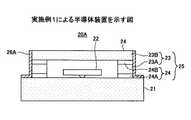
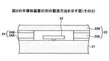
図2は、本発明の実施例2による半導体装置20を模式的に示した図である。図2を参照するに、本実施例による半導体装置20においては、基板21が実施例1の前記基板11に、素子22が実施例1の前記素子12に、さらに保護膜26が実施例1の保護膜14に相当し、同様の構造を有している。 FIG. 2 is a view schematically showing a
本実施例において、実施例1の封止構造体13に相当する封止構造体25は、無機材料よりなる無機材料部23と、有機材料よりなる有機材料部24とが組み合わされた構造となっている。さらに、前記有機材料部24を含む前記封止構造体25の外側の表面から基板21の上面には、前記保護膜26が形成されている。 In this example, the sealing
このように、本実施例による封止構造体では、有機材料と無機材料の組み合わせにより形成されており、例えば複数の無機材料よりなる部品が、有機材料により接合された構造となっている。このため、例えば無機材料で一体的に封止構造体を形成する場合に比べて、無機材料部の個々の部品の形状が単純となるため、封止構造体の製造が容易となり、製造コストを抑制できる効果を奏する。 Thus, the sealing structure according to the present embodiment is formed by a combination of an organic material and an inorganic material, and has a structure in which, for example, parts made of a plurality of inorganic materials are joined by an organic material. For this reason, compared with the case where the sealing structure is integrally formed of, for example, an inorganic material, the shape of each component of the inorganic material portion is simplified, so that the manufacturing of the sealing structure is facilitated and the manufacturing cost is reduced. The effect which can be suppressed is produced.
例えば、前記無機材料部23は、前記基板21と対向するように設置される平板上の天井部23Bと、該天井部23Bを支持する前記基板11上に設置される支持部23Aと、より構成されている。前記支持部23Aは、例えば、前記素子22を囲む空間が内部に形成された、略四角柱形状(枠状)を有している。 For example, the
また、前記有機材料部24は、例えば樹脂材料などの有機材料を主成分とする接着剤層24A、24Bよりなる。前記接着剤層24Bは、前記天井部23Bと前記支持部23Aを接合し、前記接着剤層24Aは、前記支持部23Aと前記基板21を接合している。 The
前記素子22を気密封止するための保護膜26は、前記封止構造体25の外側(前記素子22に面する側の反対側)の表面と前記基板21上面に形成されている。すなわち、前記保護膜26は、前記接着剤層24A,24Bと、前記支持部23A,前記天井部23B、および前記基板21上面に形成されている。前記保護膜26は、特に、気体の透過率が大きく気密性が十分ではない有機材料部24(前記接着剤層24A,24B)での気体の透過を抑制し、素子が封止された空間の気密性を良好としている。 A
このように、気密性に優れる前記保護膜26を前記封止構造体25に形成することで、前記封止構造体25を、有機材料と無機材料の組み合わせにより形成することが可能になっている。このため、有機材料よりなる接着剤を用いて、気密性に優れた封止構造体を形成することが可能となり、封止構造体の構造の自由度が飛躍的に向上している。 As described above, by forming the
例えば、無機材料を用いて陽極接合などの接合方法により形成される従来の封止構造体に比べて、本実施例による封止構造体は形成が容易であり、低コストで形成することが可能である。 For example, the sealing structure according to this embodiment is easier to form and can be formed at lower cost than a conventional sealing structure formed by a bonding method such as anodic bonding using an inorganic material. It is.
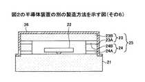
また、図3は、本発明の実施例3による半導体装置20Aを模式的に示した図である。ただし図中、先に説明した部分には同一の参照符号を付し、説明を省略する。図3を参照するに、本実施例の場合、実施例2の保護膜26に相当する保護膜26Aは、前記接着剤層24A,24Bの側面と、前記支持部23Aの側面,前記天井部23Bの側面、および前記基板22の上面に形成されているが、前記天井部23Bの、前記素子22上の面には形成されていない。 FIG. 3 is a diagram schematically showing a
例えば、前記素子22が光機能素子(例えば発光、光電変換、反射、などの機能を有する素子)の場合、前記天井部23Bを介して前記素子22に光が入射するか、または前記天井部23Bを介して前記素子22から光が照射されるため、前記天井部23Bの、前記素子22上の面は、光透過面となる。このため、当該光透過面には、保護膜が形成されずに保護膜より露出していることが好ましい。 For example, when the
また、当該光透過面に保護膜を形成する場合には、例えば反射防止膜として、または所定の波長の光をカットするフィルターとして機能するように、所定の光学特性を有するようにして形成してもよい。 In addition, when a protective film is formed on the light transmission surface, for example, it is formed so as to have a predetermined optical characteristic so as to function as an antireflection film or a filter that cuts light of a predetermined wavelength. Also good.
なお、実施例1に示した基板11、実施例2および実施例3に示した基板21には、搭載される素子(素子12、22)と外部との電気的接続をとるための配線や外部接続端子が形成されていてもよい。 Note that the
また、実施例1〜実施例3に示した半導体装置においては、封止されて保護される素子はMEMS素子に限定されるものではなく、他の様々な半導体素子であってもよい。例えば、光電変換素子(例えばフォトダイオード)や発光素子(例えばLED)などの光機能素子は、受光面または発光面がごみやほこりなどから保護されることが好ましい。このため、当該光機能素子は、実施例1〜実施例3の構造により、保護されることが好ましい。 In the semiconductor devices shown in the first to third embodiments, the element to be sealed and protected is not limited to the MEMS element, but may be various other semiconductor elements. For example, in an optical functional element such as a photoelectric conversion element (for example, a photodiode) or a light emitting element (for example, an LED), the light receiving surface or the light emitting surface is preferably protected from dust or dust. For this reason, it is preferable that the said optical function element is protected by the structure of Example 1-3.
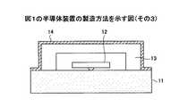
次に、図1に示した半導体装置10の製造方法の一例について、図4Aから図4Cに基づき、手順を追って説明する。なお、図中、先に説明した部分には同一の参照符号を付している。 Next, an example of a method for manufacturing the
まず、図4Aに示す工程において、例えばシリコンや、またはGaAsなどの半導体よりなる基板11上に、例えばMEMS素子などよりなる素子12を形成する。また、本工程においては、配線基板よりなる基板11上に素子12を搭載して配線を接続するようにしてもよい。 First, in the step shown in FIG. 4A, an
次に、図4Bに示す工程において、前記基板11上に、例えば一面が開口された筐体形状を有する、樹脂材料よりなる封止構造体13を設置し、開口された側の面を、例えば樹脂系の接着剤(図示せず)により、前記基板11上に接合して素子12を封止する構造とする。 Next, in the step shown in FIG. 4B, on the
次に、図4Cに示す工程において、前記封止構造体13の外側(前記素子12に面する側の反対側)の表面から基板11の上面にかけて、無機材料よりなる保護膜14を、例えばスパッタリング法により、形成する。また、保護膜14は、スパッタリング法に限定されず、CVD法などを用いて形成してもよい。また、当該保護膜14を構成する無機材料としては、例えば金属材料としては、Ti、Ni、Cr、Arなど、非金属材料としては、SiN,SiON,Si3N4,SiO2、などの材料を用いることが可能である。Next, in the step shown in FIG. 4C, a
このようにして、実施例1の図1に示した半導体装置10を形成することができる。 In this way, the
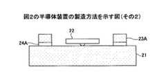
次に、図2に示した半導体装置20の製造方法の一例について、図5Aから図5Dに基づき、手順を追って説明する。なお、図中、先に説明した部分には同一の参照符号を付している。 Next, an example of a method for manufacturing the
まず、図5Aに示す工程において、例えばシリコンや、またはGaAsなどの半導体よりなる基板21上に、例えばMEMS素子などよるなる素子22を形成する。また、本工程においては、配線基板よりなる基板21上に素子22を搭載して配線を接続するようにしてもよい。 First, in the step shown in FIG. 5A, an
次に、図5Bに示す工程において、前記基板21上に、無機材料よりなる支持部23Aと前記基板21とを、例えば樹脂系の接着剤よりなる接着剤層24Aにより、接合する。 Next, in the step shown in FIG. 5B, the
次に、図5Cに示す工程において、例えば平板状の無機材料よりなる前記天井部23Bと、前記支持部23Aとを、例えば樹脂系の接着剤よりなる接着剤層24Bにより接合する。 Next, in the step shown in FIG. 5C, the
次に、図5Dに示す工程において、前記封止構造体25の外側(前記素子22に面する側の反対側)の表面と基板21上面に、無機材料よりなる保護膜26を、図4Cで先に説明した場合と同様の方法、材料により形成する。このようにして、実施例2の図2に示した半導体装置20を形成することができる。 Next, in the step shown in FIG. 5D, a
また、実施例3の図3に示した半導体装置20Aを形成する場合には、上記の図5Cに示す工程において、前記天井部23B上に、マスク層を形成し、次いで保護膜26Aを形成し、その後、マスク層を除去すればよい。 Further, when forming the
また、上記の半導体装置10、20、20Aを形成する場合には、基板上に素子が封止される構造を多数形成した後、ダイシングにより個片化する方法が一般的に用いられる。 When forming the
例えば、図6は、上記の図5Bの工程において、前記基板21上に、前記支持部23Aが接合された状態を示す斜視図である。この後で、当該貫通穴を覆うように前記天井部23Bが接合され、さらに保護層が形成された後、ダイシングされて個片化される。 For example, FIG. 6 is a perspective view showing a state in which the
例えば、無機材料を用いて一体的に前記封止構造体25に相当する構造を形成する場合には、エッチング(切削)に時間とコストがかかる問題があった。本実施例による製造方法では、このように個々の形状が単純である部品を組み合わせて封止構造体を構成することが可能となっているため、半導体装置の製造が容易となり、製造コストが低減される効果がある。 For example, when a structure corresponding to the sealing
また、半導体装置20を製造する場合には、以下に示す方法によっても形成することが可能であり、この場合、半導体装置を構成するための個々の部品の形状がさらに単純になって、半導体装置の製造コストがさらに抑制される。 Further, when the
次に、図2に示した半導体装置20の製造方法の別の一例について、図7Aから図7Fに基づき、手順を追って説明する。なお、図中、先に説明した部分には同一の参照符号を付している。 Next, another example of the manufacturing method of the
まず、図7Aに示す工程において、例えばシリコンや、またはGaAsなどの半導体よりなる基板21上に、例えばMEMS素子などよるなる素子22を形成する。また、本工程においては、配線基板よりなる基板21上に素子22を搭載して配線を接続するようにしてもよい。 First, in the step shown in FIG. 7A, an
次に、図7Bに示す工程において、前記基板21上に、無機材料よりなる支持部23Aと前記基板21とを、例えば樹脂系の接着剤よりなる接着剤層24Aにより、接合する。本実施例の場合、支持部23Aは、素子22を収容する複数の貫通孔を有する平板状である点で実施例5記載の方法と相違する。 Next, in the step shown in FIG. 7B, the
次に、図7Cに示す工程において、例えば平板状の無機材料よりなる前記天井部23Bと、前記支持部23Aとを、例えば樹脂系の接着剤よりなる接着剤層24Bにより接合する。 Next, in the step shown in FIG. 7C, the
次に、図7Dに示す工程において、隣接して形成される、複数の半導体装置の境界部に、基板21が露出するように溝部25Aを形成する。前記溝部25Aは、例えばウェハのダイシングに用いるダイサーにより、支持部23A、天井部23Bを切断して形成する。また、前記溝部25Aを形成する場合、基板21の表面が多少切削されるようにすると、後工程で保護膜により接着剤層24Aを完全に被覆することが可能となるため、封止性が向上し、好適である。 Next, in the step shown in FIG. 7D, a
次に、図7Eに示す工程において、前記天井部23B上と、前記溝部25Aの内壁面に、無機材料よりなる保護膜26を、図4Cで先に説明した場合と同様の方法、材料により形成する。その後、前記溝部25Aの底部より基板21を切断する。この場合、切断は、図中に示す切断線25Bにそって、例えばウェハのダイシングに用いるダイサーにより、行う。 Next, in the step shown in FIG. 7E, a
このようにして、図7Fに示す、半導体装置を形成することができる。本実施例の場合、支持部23Aと天井部23Bの切断(溝部25Bの形成)を、支持部23Aと天井部23Bの接合の後に行っており、接合前の構造が単純な形状(平板)の組み合わせとなるメリットがある。 In this manner, the semiconductor device shown in FIG. 7F can be formed. In the case of the present embodiment, cutting of the
以上、本発明を好ましい実施例について説明したが、本発明は上記の特定の実施例に限定されるものではなく、特許請求の範囲に記載した要旨内において様々な変形・変更が可能である。 Although the present invention has been described with reference to the preferred embodiments, the present invention is not limited to the specific embodiments described above, and various modifications and changes can be made within the scope described in the claims.
本発明によれば、基板上で素子が封止される構造を有する半導体装置であって、単純な構造で当該素子の封止の気密性が良好となるよう構成されている半導体装置と、当該半導体装置を製造する製造方法を提供することが可能となる。 According to the present invention, there is provided a semiconductor device having a structure in which an element is sealed on a substrate, the semiconductor device being configured to have a simple structure and good hermetic sealing of the element, A manufacturing method for manufacturing a semiconductor device can be provided.
10,20,20A 半導体装置
11,21 基板
12,22 素子
13,25 封止構造体
14,26 保護膜
23A 支持部
23B 天井部
23 無機材料部
24A,24B 接着剤層
24 有機材料部
25A 溝部
DESCRIPTION OF
Claims (8)
Translated fromJapanese前記基板上の素子と、
前記素子を封止する封止構造体と、を有し、
前記封止構造体は有機材料より形成されている有機材料部を含み、該有機材料部には、無機材料よりなる保護膜が形成されていることを特徴とする半導体装置。A substrate,
Elements on the substrate;
A sealing structure for sealing the element,
2. The semiconductor device according to claim 1, wherein the sealing structure includes an organic material portion made of an organic material, and a protective film made of an inorganic material is formed on the organic material portion.
前記基板上の前記素子を、有機材料よりなる部分を含む前記封止構造体により封止する工程と、
少なくとも前記有機材料よりなる部分に無機材料よりなる保護膜を形成する工程と、を有することを特徴とする半導体装置の製造方法。A method for manufacturing a semiconductor device in which an element on a substrate is sealed with a sealing structure to form a semiconductor device,
Sealing the element on the substrate with the sealing structure including a portion made of an organic material;
And a step of forming a protective film made of an inorganic material at least on a portion made of the organic material.
The method of manufacturing a semiconductor device according to claim 7, wherein the element is a MEMS element.
Priority Applications (3)
| Application Number | Priority Date | Filing Date | Title |
|---|---|---|---|
| JP2005196672AJP2007019107A (en) | 2005-07-05 | 2005-07-05 | Semiconductor device and its manufacturing method |
| US11/475,612US20070029562A1 (en) | 2005-07-05 | 2006-06-27 | Semiconductor device and method of manufacturing a semiconductor device |
| EP06253378AEP1741668A3 (en) | 2005-07-05 | 2006-06-28 | Method for encasing a MEMS device and packaged device |
Applications Claiming Priority (1)
| Application Number | Priority Date | Filing Date | Title |
|---|---|---|---|
| JP2005196672AJP2007019107A (en) | 2005-07-05 | 2005-07-05 | Semiconductor device and its manufacturing method |
Publications (1)
| Publication Number | Publication Date |
|---|---|
| JP2007019107Atrue JP2007019107A (en) | 2007-01-25 |
Family
ID=37114532
Family Applications (1)
| Application Number | Title | Priority Date | Filing Date |
|---|---|---|---|
| JP2005196672APendingJP2007019107A (en) | 2005-07-05 | 2005-07-05 | Semiconductor device and its manufacturing method |
Country Status (3)
| Country | Link |
|---|---|
| US (1) | US20070029562A1 (en) |
| EP (1) | EP1741668A3 (en) |
| JP (1) | JP2007019107A (en) |
Cited By (7)
| Publication number | Priority date | Publication date | Assignee | Title |
|---|---|---|---|---|
| JP2011049310A (en)* | 2009-08-26 | 2011-03-10 | Kyocera Chemical Corp | Hollow package for electronic component and method for manufacturing the same |
| JP2012033615A (en)* | 2010-07-29 | 2012-02-16 | Mitsubishi Electric Corp | Semiconductor device and method of manufacturing the same |
| JP2012054288A (en)* | 2010-08-31 | 2012-03-15 | Murata Mfg Co Ltd | Method for manufacturing electronic component package |
| US9102513B1 (en) | 2014-01-29 | 2015-08-11 | Himax Display, Inc. | MEMS package structure |
| JP2015160286A (en)* | 2014-02-27 | 2015-09-07 | 立景光電股▲ふん▼有限公司 | Mems mounting structure |
| US9409766B2 (en) | 2014-01-29 | 2016-08-09 | Himax Display, Inc. | MEMS package structure and manufacturing method thereof |
| JP2017181626A (en)* | 2016-03-29 | 2017-10-05 | セイコーエプソン株式会社 | Electro-optical device, manufacturing method for the same, and electronic apparatus |
Families Citing this family (24)
| Publication number | Priority date | Publication date | Assignee | Title |
|---|---|---|---|---|
| US7901989B2 (en) | 2006-10-10 | 2011-03-08 | Tessera, Inc. | Reconstituted wafer level stacking |
| US7829438B2 (en) | 2006-10-10 | 2010-11-09 | Tessera, Inc. | Edge connect wafer level stacking |
| US8513789B2 (en) | 2006-10-10 | 2013-08-20 | Tessera, Inc. | Edge connect wafer level stacking with leads extending along edges |
| US7952195B2 (en) | 2006-12-28 | 2011-05-31 | Tessera, Inc. | Stacked packages with bridging traces |
| JP5572089B2 (en) | 2007-07-27 | 2014-08-13 | テッセラ,インコーポレイテッド | Reconfigured wafer stack packaging with pad extension after application |
| US8551815B2 (en) | 2007-08-03 | 2013-10-08 | Tessera, Inc. | Stack packages using reconstituted wafers |
| US8043895B2 (en) | 2007-08-09 | 2011-10-25 | Tessera, Inc. | Method of fabricating stacked assembly including plurality of stacked microelectronic elements |
| WO2009038686A2 (en)* | 2007-09-14 | 2009-03-26 | Tessera Technologies Hungary Kft. | Hermetic wafer level cavity package |
| JP5639052B2 (en) | 2008-06-16 | 2014-12-10 | テッセラ,インコーポレイテッド | Edge stacking at wafer level |
| WO2010104610A2 (en) | 2009-03-13 | 2010-09-16 | Tessera Technologies Hungary Kft. | Stacked microelectronic assemblies having vias extending through bond pads |
| DE102010036217B4 (en)* | 2010-08-27 | 2014-02-20 | Fraunhofer-Gesellschaft zur Förderung der angewandten Forschung e.V. | Method for the hermetic encapsulation of a microsystem |
| US9887562B2 (en)* | 2012-12-03 | 2018-02-06 | Covidien Lp | Smart cart |
| US20150262902A1 (en) | 2014-03-12 | 2015-09-17 | Invensas Corporation | Integrated circuits protected by substrates with cavities, and methods of manufacture |
| US9481572B2 (en) | 2014-07-17 | 2016-11-01 | Texas Instruments Incorporated | Optical electronic device and method of fabrication |
| WO2016077723A1 (en)* | 2014-11-13 | 2016-05-19 | Armor Dental, Corp. | Oral dental shield and system |
| JP2016161472A (en)* | 2015-03-04 | 2016-09-05 | セイコーエプソン株式会社 | PHYSICAL QUANTITY SENSOR AND ITS MANUFACTURING METHOD, ELECTRONIC DEVICE, AND MOBILE BODY |
| US10002844B1 (en) | 2016-12-21 | 2018-06-19 | Invensas Bonding Technologies, Inc. | Bonded structures |
| FR3061404B1 (en)* | 2016-12-27 | 2022-09-23 | Packaging Sip | METHOD FOR THE COLLECTIVE MANUFACTURING OF HERMETIC ELECTRONIC MODULES |
| EP3580166A4 (en) | 2017-02-09 | 2020-09-02 | Invensas Bonding Technologies, Inc. | Bonded structures |
| US10508030B2 (en) | 2017-03-21 | 2019-12-17 | Invensas Bonding Technologies, Inc. | Seal for microelectronic assembly |
| US10923408B2 (en) | 2017-12-22 | 2021-02-16 | Invensas Bonding Technologies, Inc. | Cavity packages |
| US11380597B2 (en) | 2017-12-22 | 2022-07-05 | Invensas Bonding Technologies, Inc. | Bonded structures |
| US11004757B2 (en) | 2018-05-14 | 2021-05-11 | Invensas Bonding Technologies, Inc. | Bonded structures |
| US12374641B2 (en) | 2019-06-12 | 2025-07-29 | Adeia Semiconductor Bonding Technologies Inc. | Sealed bonded structures and methods for forming the same |
Citations (3)
| Publication number | Priority date | Publication date | Assignee | Title |
|---|---|---|---|---|
| JPS54114569A (en)* | 1978-02-28 | 1979-09-06 | Japan Steel Works Ltd | Screw for biaxial extruder |
| JPH06224318A (en)* | 1993-01-26 | 1994-08-12 | Kyocera Corp | Semiconductor device |
| JP2005167129A (en)* | 2003-12-05 | 2005-06-23 | Matsushita Electric Ind Co Ltd | Electronic device package and method of manufacturing electronic device package |
Family Cites Families (7)
| Publication number | Priority date | Publication date | Assignee | Title |
|---|---|---|---|---|
| US4939316A (en)* | 1988-10-05 | 1990-07-03 | Olin Corporation | Aluminum alloy semiconductor packages |
| US6661084B1 (en)* | 2000-05-16 | 2003-12-09 | Sandia Corporation | Single level microelectronic device package with an integral window |
| JP2002231918A (en)* | 2001-02-06 | 2002-08-16 | Olympus Optical Co Ltd | Solid-state imaging device and manufacturing method thereof |
| US6641254B1 (en)* | 2002-04-12 | 2003-11-04 | Hewlett-Packard Development Company, L.P. | Electronic devices having an inorganic film |
| US20040108588A1 (en)* | 2002-09-24 | 2004-06-10 | Cookson Electronics, Inc. | Package for microchips |
| JP4271625B2 (en)* | 2004-06-30 | 2009-06-03 | 株式会社フジクラ | Semiconductor package and manufacturing method thereof |
| US7424198B2 (en)* | 2004-09-27 | 2008-09-09 | Idc, Llc | Method and device for packaging a substrate |
- 2005
- 2005-07-05JPJP2005196672Apatent/JP2007019107A/enactivePending
- 2006
- 2006-06-27USUS11/475,612patent/US20070029562A1/ennot_activeAbandoned
- 2006-06-28EPEP06253378Apatent/EP1741668A3/ennot_activeWithdrawn
Patent Citations (3)
| Publication number | Priority date | Publication date | Assignee | Title |
|---|---|---|---|---|
| JPS54114569A (en)* | 1978-02-28 | 1979-09-06 | Japan Steel Works Ltd | Screw for biaxial extruder |
| JPH06224318A (en)* | 1993-01-26 | 1994-08-12 | Kyocera Corp | Semiconductor device |
| JP2005167129A (en)* | 2003-12-05 | 2005-06-23 | Matsushita Electric Ind Co Ltd | Electronic device package and method of manufacturing electronic device package |
Cited By (8)
| Publication number | Priority date | Publication date | Assignee | Title |
|---|---|---|---|---|
| JP2011049310A (en)* | 2009-08-26 | 2011-03-10 | Kyocera Chemical Corp | Hollow package for electronic component and method for manufacturing the same |
| JP2012033615A (en)* | 2010-07-29 | 2012-02-16 | Mitsubishi Electric Corp | Semiconductor device and method of manufacturing the same |
| JP2012054288A (en)* | 2010-08-31 | 2012-03-15 | Murata Mfg Co Ltd | Method for manufacturing electronic component package |
| US9102513B1 (en) | 2014-01-29 | 2015-08-11 | Himax Display, Inc. | MEMS package structure |
| US9409766B2 (en) | 2014-01-29 | 2016-08-09 | Himax Display, Inc. | MEMS package structure and manufacturing method thereof |
| JP2015160286A (en)* | 2014-02-27 | 2015-09-07 | 立景光電股▲ふん▼有限公司 | Mems mounting structure |
| JP2017181626A (en)* | 2016-03-29 | 2017-10-05 | セイコーエプソン株式会社 | Electro-optical device, manufacturing method for the same, and electronic apparatus |
| CN107238923A (en)* | 2016-03-29 | 2017-10-10 | 精工爱普生株式会社 | Electro-optical device, the manufacture method of electro-optical device and electronic equipment |
Also Published As
| Publication number | Publication date |
|---|---|
| EP1741668A2 (en) | 2007-01-10 |
| EP1741668A3 (en) | 2009-04-08 |
| US20070029562A1 (en) | 2007-02-08 |
Similar Documents
| Publication | Publication Date | Title |
|---|---|---|
| JP2007019107A (en) | Semiconductor device and its manufacturing method | |
| US7633150B2 (en) | Semiconductor device and method for manufacturing semiconductor device | |
| US8017435B2 (en) | Method for packaging electronic devices and integrated circuits | |
| US7250353B2 (en) | Method and system of releasing a MEMS structure | |
| JP5154819B2 (en) | Substrate and manufacturing method thereof | |
| EP1848034A2 (en) | Electronic component device | |
| US6839962B2 (en) | Method of producing micromechanical structures | |
| JP2008119826A (en) | Airtight sealing of micro devices | |
| CN101156242A (en) | Production method of encapsulated electronic component and encapsulated electronic component | |
| US20110128082A1 (en) | Atomic oscillator and manufacturing method | |
| JP2010177375A (en) | Light-emitting device and manufacturing method of the same | |
| KR20170092955A (en) | Acoustic wave filter device, package for manufacturing acoustic wave filter device | |
| JP2012069977A (en) | Light emitting device and method for manufacturing the same | |
| JP2013154465A (en) | Mems device assembly and method of packaging the same | |
| US20170052364A1 (en) | Assembly body for micromirror chips, mirror device and production method for a mirror device | |
| CN103021965A (en) | Light-transmitting package structure and package method based on silicon substrate and glass gland | |
| US7592195B2 (en) | Method for producing a sensor or actuator arrangement, and corresponding sensor or actuator arrangement | |
| US7709940B2 (en) | Micro device encapsulation | |
| JP2007096093A (en) | Optical module | |
| CN111566818B (en) | Optical sensor manufacturing method and optical sensor | |
| JP4259979B2 (en) | Light transmissive cover, device provided with the same, and manufacturing method thereof | |
| TWI666783B (en) | Method for manufacturing optical sensor arrangements and housing for an optical sensor | |
| JP6344266B2 (en) | Semiconductor device and manufacturing method thereof | |
| CN113365938A (en) | Micromechanical sensor device and corresponding manufacturing method | |
| JP2024089445A (en) | Mems sensor and method for manufacturing mems sensor |
Legal Events
| Date | Code | Title | Description |
|---|---|---|---|
| A621 | Written request for application examination | Free format text:JAPANESE INTERMEDIATE CODE: A621 Effective date:20080513 | |
| A977 | Report on retrieval | Free format text:JAPANESE INTERMEDIATE CODE: A971007 Effective date:20100915 | |
| A131 | Notification of reasons for refusal | Free format text:JAPANESE INTERMEDIATE CODE: A131 Effective date:20100921 | |
| A521 | Written amendment | Free format text:JAPANESE INTERMEDIATE CODE: A523 Effective date:20101105 | |
| A02 | Decision of refusal | Free format text:JAPANESE INTERMEDIATE CODE: A02 Effective date:20110823 |