JP2007012855A - Semiconductor integrated circuit, standard cell, standard cell library, semiconductor integrated circuit design method, and semiconductor integrated circuit design apparatus - Google Patents
Semiconductor integrated circuit, standard cell, standard cell library, semiconductor integrated circuit design method, and semiconductor integrated circuit design apparatusDownload PDFInfo
- Publication number
- JP2007012855A JP2007012855AJP2005191433AJP2005191433AJP2007012855AJP 2007012855 AJP2007012855 AJP 2007012855AJP 2005191433 AJP2005191433 AJP 2005191433AJP 2005191433 AJP2005191433 AJP 2005191433AJP 2007012855 AJP2007012855 AJP 2007012855A
- Authority
- JP
- Japan
- Prior art keywords
- gate
- transistor
- standard cell
- semiconductor integrated
- integrated circuit
- Prior art date
- Legal status (The legal status is an assumption and is not a legal conclusion. Google has not performed a legal analysis and makes no representation as to the accuracy of the status listed.)
- Pending
Links
Images


Classifications
- H—ELECTRICITY
- H10—SEMICONDUCTOR DEVICES; ELECTRIC SOLID-STATE DEVICES NOT OTHERWISE PROVIDED FOR
- H10D—INORGANIC ELECTRIC SEMICONDUCTOR DEVICES
- H10D84/00—Integrated devices formed in or on semiconductor substrates that comprise only semiconducting layers, e.g. on Si wafers or on GaAs-on-Si wafers
- H10D84/90—Masterslice integrated circuits
- H10D84/903—Masterslice integrated circuits comprising field effect technology
- H10D84/907—CMOS gate arrays
- G—PHYSICS
- G06—COMPUTING OR CALCULATING; COUNTING
- G06F—ELECTRIC DIGITAL DATA PROCESSING
- G06F30/00—Computer-aided design [CAD]
- G06F30/30—Circuit design
- G06F30/39—Circuit design at the physical level
- G06F30/392—Floor-planning or layout, e.g. partitioning or placement
- H—ELECTRICITY
- H10—SEMICONDUCTOR DEVICES; ELECTRIC SOLID-STATE DEVICES NOT OTHERWISE PROVIDED FOR
- H10D—INORGANIC ELECTRIC SEMICONDUCTOR DEVICES
- H10D89/00—Aspects of integrated devices not covered by groups H10D84/00 - H10D88/00
- H10D89/10—Integrated device layouts
Landscapes
- Engineering & Computer Science (AREA)
- Computer Hardware Design (AREA)
- Physics & Mathematics (AREA)
- Theoretical Computer Science (AREA)
- Architecture (AREA)
- Evolutionary Computation (AREA)
- Geometry (AREA)
- General Engineering & Computer Science (AREA)
- General Physics & Mathematics (AREA)
- Semiconductor Integrated Circuits (AREA)
- Design And Manufacture Of Integrated Circuits (AREA)
- Preparing Plates And Mask In Photomechanical Process (AREA)
Abstract
Translated fromJapaneseDescription
Translated fromJapanese本発明は、光近接効果の抑制に対して有効な半導体集積回路、標準セル、標準セルライブラリ、半導体集積回路の設計方法および半導体集積回路の設計装置に関するものである。 The present invention relates to a semiconductor integrated circuit, a standard cell, a standard cell library, a semiconductor integrated circuit design method, and a semiconductor integrated circuit design apparatus that are effective for suppressing the optical proximity effect.
まず、本明細書における言葉の定義を以下に記す。 First, the definitions of words in this specification are described below.
活性トランジスタとは非活性トランジスタではないトランジスタを指す。非活性トランジスタとは、トランジスタの動作特性を利用して回路の所望の機能を実現することを期待していないトランジスタを指す。非活性トランジスタのゲート寸法がどれだけばらつこうと回路の所望の機能の実現には問題にならない。非活性トランジスタには、Pチャネルトランジスタのゲート電位を電源電位に固定したものもしくはNチャネルトランジスタのゲート電位を接地電位に固定したものであって、オフ状態に保たれているトランジスタ(以下、これをオフトランジスタと呼ぶ)や、Pチャネルトランジスタのゲート電位を接地電位に固定し、さらにソース電位およびドレイン電位を電源電位に固定したもの、もしくはNチャネルトランジスタのゲート電位を電源電位に固定し、さらにソース電位およびドレイン電位を接地電位に固定したものを電源と接地間の容量として作用させるトランジスタ(以下、これを容量トランジスタと呼ぶ)や、ソース電位とドレイン電位を同電位に固定することで電流が流れないようにしたトランジスタを含む。トランジスタとは活性トランジスタおよび非活性トランジスタの両方を指す。 An active transistor refers to a transistor that is not an inactive transistor. An inactive transistor refers to a transistor that is not expected to realize a desired function of a circuit by using the operation characteristics of the transistor. It does not matter how much the gate dimensions of the inactive transistors vary to realize the desired function of the circuit. An inactive transistor is a transistor in which the gate potential of a P-channel transistor is fixed to a power supply potential or a gate potential of an N-channel transistor is fixed to a ground potential, and is kept in an off state (hereinafter referred to as a transistor). Called the off-transistor), the gate potential of the P-channel transistor is fixed to the ground potential, the source potential and the drain potential are fixed to the power supply potential, or the gate potential of the N-channel transistor is fixed to the power supply potential, and the source A transistor in which the potential and the drain potential are fixed to the ground potential is used as a capacitor between the power source and the ground (hereinafter referred to as a capacitance transistor), or a current flows by fixing the source potential and the drain potential to the same potential. Including a transistor that is not included. Transistor refers to both active and inactive transistors.
ゲートとは、ポリシリコンなどで形成されたトランジスタのゲートと、拡散領域上に無いポリシリコンなどで形成されたダミーゲートと前記トランジスタのゲートと同じ材料で形成された拡散領域上に無い配線を含んだ概念である。 The gate includes a gate of a transistor formed of polysilicon or the like, a dummy gate formed of polysilicon or the like not on the diffusion region, and a wiring not on the diffusion region formed of the same material as the gate of the transistor. It is a concept.
半導体集積回路の設計における、伝搬遅延時間のばらつきの主な要因としては、動作電源電圧、温度、プロセス上のばらつきなどがある。半導体集積回路は、上記のばらつきの要因のすべてが最も悪い条件となった場合でもその動作を保障するように設計されていなければならない。特にトランジスタのゲート長はトランジスタの動作を規定する重要な要素であり、ゲート長のばらつきの影響は、プロセス上のばらつきの中で非常に大きな割合を占めている。さらに近年、トランジスタの微細化の進展に伴ってゲート長はますます小さくなり、ゲート長のばらつきの割合が増大する傾向にある。このため、伝搬遅延時間のばらつきが増大して設計マージンを大きくする必要が生じており、高性能な半導体集積回路を提供することが困難になっている。 The main causes of variations in propagation delay time in the design of semiconductor integrated circuits include operating power supply voltage, temperature, process variations, and the like. A semiconductor integrated circuit must be designed to ensure its operation even when all of the above-mentioned factors of variation are in the worst condition. In particular, the gate length of the transistor is an important factor that defines the operation of the transistor, and the influence of the variation in the gate length accounts for a very large proportion of the variation in the process. Furthermore, in recent years, with the progress of miniaturization of transistors, the gate length has become smaller and the variation rate of the gate length tends to increase. For this reason, it is necessary to increase the design margin by increasing the variation in propagation delay time, and it is difficult to provide a high-performance semiconductor integrated circuit.
また、一般に、半導体集積回路の製造プロセスでは、レジスト塗布、露光、現像を含むフォトリソグラフィ工程と、レジストマスクを用いて要素のパターニングを行うためのエッチング工程と、レジスト除去工程とを繰り返すことにより、半導体基板上に集積回路を形成する。トランジスタのゲートを形成する際にも、フォトリソグラフィ工程、エッチング工程、レジスト除去工程が行われる。このフォトリソグラフィ工程の露光の際に、パターン寸法が露光波長以下になると、回折光の影響による光近接効果によって、設計時のレイアウト寸法と半導体基板上のパターン寸法との誤差が大きくなる。 In general, in the manufacturing process of a semiconductor integrated circuit, by repeating a photolithography process including resist coating, exposure, and development, an etching process for patterning an element using a resist mask, and a resist removing process, An integrated circuit is formed on a semiconductor substrate. A photolithography process, an etching process, and a resist removal process are also performed when the gate of the transistor is formed. If the pattern dimension is equal to or smaller than the exposure wavelength during exposure in the photolithography process, an error between the design layout dimension and the pattern dimension on the semiconductor substrate increases due to the optical proximity effect due to the influence of diffracted light.
このため、半導体集積回路の製造に際し、半導体集積回路内に形成された配線などのパターンを描画もしくは露光するにあたって光近接効果によって生じるパターンの寸法精度の向上のための補正が不可欠になっている。光近接効果を補正する技術としてOPC(Optical Proximity effect Correction)が考えられる。OPCとは、ゲートとそれに近接する他のゲートパターンまでの距離から光近接効果によるゲート長変動量を予測し、その変動量を打ち消すようにゲートを形成するためのフォトレジストのマスク値を予め補正することによって露光後のゲート長の仕上がり値を一定値に保つ技術である。 For this reason, in manufacturing a semiconductor integrated circuit, correction for improving the dimensional accuracy of the pattern caused by the optical proximity effect is indispensable when drawing or exposing a pattern such as a wiring formed in the semiconductor integrated circuit. As a technique for correcting the optical proximity effect, OPC (Optical Proximity effect Correction) can be considered. OPC predicts the gate length fluctuation amount due to the optical proximity effect from the distance between the gate and another gate pattern adjacent to it, and corrects the mask value of the photoresist to form the gate so as to cancel the fluctuation amount in advance This is a technique for keeping the finished gate length after exposure constant.
従来のレイアウトではゲートパターンは規格化されておらず、ゲート長やゲート間隔はチップ全体でまちまちであったため、OPCによる補正をかける必要があったが、OPCによるゲートマスクの補正は、TAT(Turn Around Time)の遅延や処理量の増大を招くという問題があった。 In the conventional layout, the gate pattern was not standardized, and the gate length and gate interval were different for the entire chip.Therefore, correction by OPC was necessary, but correction of the gate mask by OPC is not possible with TAT (Turn Around Time), and there was a problem of increasing the processing amount.
これを回避するために、ゲート長やゲート間隔を統一したただ一種類の値のみを使用してレイアウトを行うといった提案もなされている。この提案によれば、ただ一種類のゲート長で回路設計を行ったり、ゲート間隔を統一するために実際には素子としての役割を果たさないダミーゲートを挿入したりすることで、確かにOPCによるゲートマスクの修正を行わずとも、ゲート長の仕上がり値を一定値に保つことができるが、一方で設計の自由度を著しく損ねるため、回路特性の劣化やチップ面積の増大を招くという問題があった。そこで、任意のゲート長やゲート間隔を使用しつつ、光近接効果によるゲート長のばらつきを抑制するための手段の確立が望まれていた。 In order to avoid this, a proposal has been made to perform the layout using only one type of value in which the gate length and the gate interval are unified. According to this proposal, circuit design with just one type of gate length, or by inserting a dummy gate that does not actually play a role as an element in order to unify the gate spacing, is certainly by OPC Even if the gate mask is not modified, the final gate length can be maintained at a constant value, but on the other hand, the degree of freedom in design is greatly impaired, leading to problems such as circuit characteristics degradation and chip area increase. It was. Accordingly, it has been desired to establish means for suppressing variations in gate length due to the optical proximity effect while using an arbitrary gate length and gate interval.
なお、この出願の発明に関連する先行技術文献情報としては、例えば、特許文献1が知られている。
先に述べたように、トランジスタの微細化の進展に伴いゲート長は短くなり、ゲートを露光する際、回折光による光近接効果の影響が大きくなる。OPC技術は、光近接効果の影響によるゲート長の仕上り寸法の周辺パターン依存性を大きく改善するが、標準セルで使われているような全ての周辺パターンに対してその依存性を完全に補正することは困難である。とはいえ、OPC技術による補正精度の向上にこだわるあまり、ゲート長やゲート間隔を統一してしまったのでは、設計の自由度を大きく損ねる結果となってしまう。 As described above, the gate length is shortened with the progress of miniaturization of the transistor, and the influence of the optical proximity effect by the diffracted light is increased when the gate is exposed. OPC technology greatly improves the peripheral pattern dependency of the gate length finish dimension due to the effect of optical proximity effect, but completely corrects that dependency for all peripheral patterns used in standard cells. It is difficult. Nonetheless, unifying the gate length and the gate interval because the improvement of the correction accuracy by the OPC technology is too much, results in a significant loss of design flexibility.
本発明の目的は、設計の自由度を確保するべく、任意のゲート長やゲート間隔の使用を許容したレイアウトにおいて、光近接効果によるゲート長のばらつきを抑制することができる半導体集積回路、標準セル、標準セルライブラリ、半導体集積回路の設計方法および半導体集積回路の設計装置を提供することにある。 An object of the present invention is to provide a semiconductor integrated circuit and a standard cell capable of suppressing variations in gate length due to the optical proximity effect in a layout that allows the use of an arbitrary gate length and gate interval in order to ensure flexibility in design. Another object of the present invention is to provide a standard cell library, a semiconductor integrated circuit design method, and a semiconductor integrated circuit design apparatus.
OPC処理は補正対象となるゲートパターンを中心としたある半径r内に含まれる周辺のゲートパターンを考慮しながら行われる。従って、この半径rを広げれば広げるほど、より多くの周辺ゲートパターンから受ける光近接効果による影響を考慮することができるため精度は向上するが、考慮する範囲が広がることにより処理量は増加してしまう。一方、あまりにもこの半径rを狭めてしまうと、光近接効果による影響を考慮しきれていないことになり精度上問題がある。 The OPC process is performed in consideration of peripheral gate patterns included in a radius r centered on the gate pattern to be corrected. Therefore, as the radius r is increased, the accuracy is improved because the influence of the optical proximity effect received from more peripheral gate patterns can be taken into account, but the processing amount increases due to the expansion of the range to be considered. End up. On the other hand, if the radius r is too narrow, the influence of the optical proximity effect cannot be considered, and there is a problem in accuracy.
そこで通常は、補正対象となるゲートからどれくらい離れている周辺ゲートによる光近接効果であれば、補正対象となるゲートの仕上がり寸法ばらつきに与える影響を無視することができるかを見きわめ、精度と処理量のバランスを取れるよう半径rを設定している。なお、半径rを設定する際には、半径r内に存在する周辺ゲートパターンがいかなる形状であろうとも、OPCを用いることで、補正対象となるゲートパターンの仕上がり形状ばらつきを所望の範囲内に収めることができるよう設定するのが一般的である。 Therefore, it is normal to determine how far away from the gate to be corrected the optical proximity effect is due to the peripheral gate, which can ignore the effect on the variation in the finished dimensions of the gate to be corrected, accuracy and throughput. The radius r is set so that When setting the radius r, regardless of the shape of the peripheral gate pattern existing in the radius r, the OPC is used to bring the variation in the finished shape of the gate pattern to be corrected within the desired range. Generally, it is set so that it can be accommodated.
このとき、仮に半径r内に存在する周辺ゲートパターンを限定することができれば、任意の周辺ゲートパターンが存在する可能性のあることを前提とした場合に比べて、よりゲートパターンの仕上がり形状ばらつきを抑えることができる。なぜならば、ゲートが等長等間隔で整然と並んだ場合や、補正対象となるゲートパターンに近接して周辺ゲートパターンが配置されていない場合に比べて、例えば補正対象となるゲートパターンに隣接して極端にゲート長の大きいゲートを配置した場合には補正対象となるゲートの仕上がり寸法のばらつきは大きくなるため、こうしたばらつきの大きくなる要因となるゲートを補正対象となるゲートの周辺に配置しないように工夫することでばらつきを抑えられるからである。 At this time, if the peripheral gate pattern existing within the radius r can be limited, the variation in the finished shape of the gate pattern can be further improved compared to the case where there is a possibility that an arbitrary peripheral gate pattern exists. Can be suppressed. This is because, for example, adjacent to the gate pattern to be corrected, compared to the case where the gates are regularly arranged at equal intervals, or when the peripheral gate pattern is not disposed adjacent to the gate pattern to be corrected. If a gate with an extremely long gate length is placed, the variation in the finished dimensions of the gate to be corrected will increase, so do not place the gate that causes such variation around the gate to be corrected. This is because the variation can be suppressed by devising.
図22、図23を用いてさらに詳しく説明する。図22はゲートのレイアウトパターンの平面図であり、L1, L2はゲートである。ゲートL2のゲート長はゲートL1のゲート長より大きい。図23はゲートL1に対してゲートL2を間隔Sで配置した場合の、ゲートL1のゲート長の仕上がり寸法を表した特性図の一例である。 This will be described in more detail with reference to FIGS. FIG. 22 is a plan view of a layout pattern of gates, and L1 and L2 are gates. The gate length of the gate L2 is larger than the gate length of the gate L1. FIG. 23 is an example of a characteristic diagram showing the finished dimensions of the gate length of the gate L1 when the gate L2 is arranged at an interval S with respect to the gate L1.
図23の縦軸は理想的なゲートL1のゲート長のパターン寸法に対するゲートL1のゲート長の仕上がり寸法の比率kを、横軸は間隔S[um]を表す。ここで理想的なゲート長のパターン寸法とは、ゲートが最小ゲート長最小ゲート間隔で整然と並び光近接効果によるゲート長のばらつきが最小に抑えられた場合のゲート長の寸法をいう。図23に示すように、間隔Sがデザインルールで規定された最小値Sminである場合、ゲートL1のゲート長の仕上がり寸法は理想的なパターン寸法に対しkmin倍小さくなり、レイアウト寸法と半導体集積回路上のパターン寸法との誤差が非常に大きくなるのに対し、間隔をSpに広げた場合、ゲートL1のゲート長の仕上がり寸法はkp倍程度に抑えられる。 The vertical axis in FIG. 23 represents the ratio k of the finished dimension of the gate length of the gate L1 to the ideal gate length pattern dimension of the gate L1, and the horizontal axis represents the interval S [um]. Here, the ideal gate length pattern dimension means a gate length dimension when the gates are arranged in an orderly manner with a minimum gate length and a minimum gate interval, and variations in the gate length due to the optical proximity effect are suppressed to a minimum. As shown in FIG. 23, when the interval S is the minimum value Smin specified by the design rule, the finished gate length of the gate L1 is kmin times smaller than the ideal pattern dimension, and the layout dimension and the semiconductor integrated circuit While the error from the above pattern dimension becomes very large, when the interval is widened to Sp, the finished dimension of the gate length of the gate L1 can be suppressed to about kp times.
これはゲートL1とゲートL2の間隔を広げることにより、ゲートL2がゲートL1に与える光近接効果による影響を緩和することができるためである。このように、たとえ隣接するゲートの幅が大きい場合であっても、隣接するゲートとの間隔を広げることにより、ゲート長の仕上がり寸法のばらつきを抑えられる。また、ゲートL1とゲートL2の間を広げ、その間にダミーゲートを挿入した場合には、半径r内においてゲートが等長等間隔で並んでいる場合と似た状況と見なせるため、同様にゲートL2がゲートL1に与える光近接効果による影響を緩和することができる。通常の半導体集積回路の設計においては、レイアウト寸法と半導体集積回路上のパターン寸法とが一致する、あるいは、ある一定のオフセット値分だけ異なることを前提としており、この前提と異なるパターン寸法に仕上がった場合、設計時のタイミング検証において動作確認を行っていたにも関わらず、実際の半導体集積回路が動作しないといった不具合が発生する恐れがある。このため、所望のパターン形状が得られるように、光近接効果による影響を緩和することでゲート長のばらつきを抑制することの意味は大きい。 This is because the influence of the optical proximity effect that the gate L2 has on the gate L1 can be reduced by increasing the distance between the gate L1 and the gate L2. As described above, even if the width of the adjacent gate is large, it is possible to suppress the variation in the finished dimension of the gate length by increasing the interval between the adjacent gates. In addition, when the space between the gates L1 and L2 is widened and a dummy gate is inserted between them, the situation can be regarded as similar to the case where the gates are arranged at equal intervals within the radius r. Can alleviate the influence of the optical proximity effect on the gate L1. In normal semiconductor integrated circuit design, it is assumed that the layout dimensions and the pattern dimensions on the semiconductor integrated circuit match or differ by a certain offset value. In this case, there is a possibility that a problem such as the fact that the actual semiconductor integrated circuit does not operate although the operation is confirmed in the timing verification at the time of design may occur. For this reason, it is significant to suppress variations in gate length by reducing the influence of the optical proximity effect so that a desired pattern shape can be obtained.
本発明は、以上の知見を基にしており、半導体集積回路の形成に際して、活性なトランジスタとそれに近接するゲートとの間隔を広げることを特徴とする。具体的には、標準セル内の活性なトランジスタとこれに近接するゲートとの距離を離す、あるいは、標準セル内の活性なトランジスタとセル枠との距離を離す、あるいは、活性なトランジスタを含む標準セルに隣接して、活性なトランジスタを含まないスペーサー標準セルを配置するといった手段により間隔を広げる。 The present invention is based on the above knowledge, and is characterized in that in forming a semiconductor integrated circuit, the interval between an active transistor and a gate adjacent thereto is increased. Specifically, the active transistor in the standard cell is separated from the gate adjacent thereto, or the active transistor in the standard cell is separated from the cell frame, or the standard including the active transistor is included. The space is widened by means such as placing a spacer standard cell that does not include an active transistor adjacent to the cell.
以上のような本発明の半導体集積回路、標準セル、標準セルライブラリ、半導体集積回路の設計方法および半導体集積回路の設計装置によれば、OPC処理を行う際に補正対象となる活性トランジスタ上のゲートパターンに近接して配置する周辺ゲートパターンを限定できることになり、任意の周辺ゲートパターンが存在することを前提とした場合に比べて、補正対象となるゲートパターンの仕上がり形状のばらつきを抑えることができる。 According to the semiconductor integrated circuit, the standard cell, the standard cell library, the semiconductor integrated circuit design method and the semiconductor integrated circuit design apparatus of the present invention as described above, the gate on the active transistor to be corrected when performing the OPC process Peripheral gate patterns placed close to the pattern can be limited, and variations in the finished shape of the gate pattern to be corrected can be suppressed compared to the assumption that there is an arbitrary peripheral gate pattern. .
以下、本発明にかかわる半導体集積回路、標準セル、標準セルライブラリ、半導体集積回路の設計方法および半導体集積回路の設計装置の実施の形態を図面に基づいて詳細に説明する。 Embodiments of a semiconductor integrated circuit, a standard cell, a standard cell library, a semiconductor integrated circuit design method, and a semiconductor integrated circuit design apparatus according to the present invention will be described below in detail with reference to the drawings.
(第一の実施の形態)
図1を用いて第一の実施の形態を説明する。図1は、本発明の第一の実施の形態の半導体集積回路のレイアウトパターンの簡略図である。ゲート1a1と拡散領域1a2によって形成された活性トランジスタ1a、ゲート1b1と拡散領域1b2によって形成されたトランジスタ1b、ゲート1c1が、活性トランジスタ1aを中心に、その両側に配置されている。(First embodiment)
The first embodiment will be described with reference to FIG. FIG. 1 is a simplified diagram of the layout pattern of the semiconductor integrated circuit according to the first embodiment of the present invention. An active transistor 1a formed by the gate 1a1 and the diffusion region 1a2, a
ここで、ゲート1a1とゲート1b1との間隔を1S1、ゲート1a1とゲート1c1との間隔を1S2とした場合、1S1が1S2より大きくなるようにゲートを配置する。このようにゲート1a1と1b1の間隔を広げて配置することにより、トランジスタ1bのゲート1b1が活性トランジスタ1aのゲート1a1に与える光近接効果を緩和することができるため、ゲート1a1の仕上がり寸法ばらつきを抑えることが出来る。 Here, when the interval between the gate 1a1 and the gate 1b1 is 1S1, and the interval between the gate 1a1 and the gate 1c1 is 1S2, the gates are arranged so that 1S1 is larger than 1S2. By disposing the gates 1a1 and 1b1 in such a wide manner as described above, the optical proximity effect that the gate 1b1 of the
(第二の実施の形態)
図2を用いて、第二の実施の形態を説明する。図2は、本発明の第二の実施の形態の半導体集積回路のレイアウトパターンの簡略図である。図1に対して図2の異なる点は、ゲート2c1がダミーゲートとなっている点である。このようにゲート2c1がダミーゲートの場合でも、上記第一の実施の形態のようにゲート2a1とゲート2b1の間隔を広げる効果は、第一の実施の形態の場合と同様である。(Second embodiment)
A second embodiment will be described with reference to FIG. FIG. 2 is a simplified diagram of the layout pattern of the semiconductor integrated circuit according to the second embodiment of the present invention. 2 differs from FIG. 1 in that the gate 2c1 is a dummy gate. As described above, even when the gate 2c1 is a dummy gate, the effect of widening the distance between the gate 2a1 and the gate 2b1 as in the first embodiment is the same as that in the first embodiment.
(第三の実施の形態)
図3を用いて第三の実施の形態を説明する。図3は、本発明の第三の実施の形態の半導体集積回路のレイアウトパターンの簡略図である。図1に対して図3の異なる点は、活性トランジスタ3aのゲート3a1とトランジスタ3bのゲート3b1間に、ダミーゲート3d1がゲート3a1と平行に配置されている点である。図3のように、活性トランジスタ3aのゲート3a1とトランジスタ3bのゲート3b1の間に別のゲート3d1を挟むことにより、トランジスタ3bのゲート3b1が活性トランジスタ3aのゲート3a1に与える光近接効果による仕上がり寸法ばらつきへの影響を、第一の実施の形態以上に抑えることが出来る。(Third embodiment)
A third embodiment will be described with reference to FIG. FIG. 3 is a simplified diagram of the layout pattern of the semiconductor integrated circuit according to the third embodiment of the present invention. 3 differs from FIG. 1 in that a dummy gate 3d1 is arranged in parallel with the gate 3a1 between the gate 3a1 of the active transistor 3a and the gate 3b1 of the transistor 3b. As shown in FIG. 3, when another gate 3d1 is sandwiched between the gate 3a1 of the active transistor 3a and the gate 3b1 of the transistor 3b, the finished size due to the optical proximity effect that the gate 3b1 of the transistor 3b gives to the gate 3a1 of the active transistor 3a The influence on the variation can be suppressed more than in the first embodiment.
なお、上記第三の実施の形態において、図3のゲート3a1,3b1,3c1,ダミーゲート3d1のゲート長を等長とし、かつ等間隔の配置にすると、課題を解決するための手段で述べた通り、光近接効果によるゲートの仕上がり寸法ばらつきを、さらに抑えることができ、この時、図3の3S1は3S2の2倍以上となる。 In the third embodiment, when the gate lengths of the gates 3a1, 3b1, 3c1, and the dummy gate 3d1 in FIG. 3 are equal and arranged at equal intervals, the means for solving the problem is described. As can be seen, variations in the gate finish due to the optical proximity effect can be further suppressed. At this time, 3S1 in FIG. 3 is more than twice as large as 3S2.
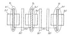
(第四の実施の形態)
図4を用いて、第四の実施の形態を説明する。図4は、本発明の第四の実施の形態の半導体集積回路のレイアウトパターンの簡略図である。ゲート4a1と拡散領域4a2によって形成された活性トランジスタ4a、ゲート4b1と拡散領域4b2によって形成されたトランジスタ4b、ゲート4c1が、活性トランジスタ4aを中心に、その両側に配置され、活性トランジスタ4aとトランジスタ4bの間に、ダミーゲート4d1,4e1がゲート4a1と平行に配置されている。ここで、ゲート4a1とゲート4b1との間隔を4S1、ゲート4a1とゲート4c1との間隔を4S2としたとき、4S1が4S2より大きくなるようにゲートを配置する。図3に対して図4の異なる点は、トランジスタ4aのゲート4a1とトランジスタ4bのゲート4b1の間にあるダミーゲートが複数本となっている点である。このようにトランジスタ間のゲート本数が増えるとトランジスタ4bのゲート4b1が活性トランジスタ4aのゲート4a1に与える光近接効果による仕上がり寸法ばらつきの影響を抑えることが出来る。(Fourth embodiment)
A fourth embodiment will be described with reference to FIG. FIG. 4 is a simplified diagram of the layout pattern of the semiconductor integrated circuit according to the fourth embodiment of the present invention. The
なお、上記第四の実施の形態において、図4のゲート4a1,4b1,4c1,ダミーゲート4d1,4e1のゲート長を等長とし、かつ等間隔の配置にすると、光近接効果によるゲートの仕上がり寸法ばらつきを更に抑えることができ、この時、図4の4S1は4S2の3倍以上となる。 In the fourth embodiment, when the gate lengths of the gates 4a1, 4b1, 4c1 and dummy gates 4d1, 4e1 in FIG. 4 are made equal and spaced, the finished dimensions of the gate due to the optical proximity effect The variation can be further suppressed. At this time, 4S1 in FIG. 4 is more than three times 4S2.
(第五の実施の形態)
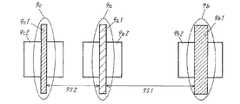
第五の実施の形態として、第四の実施の形態が最も効果的な一例を、図5を用いて説明する。図5は、本発明の第五の実施の形態の半導体集積回路のレイアウトパターンの簡略図である。図4に対して図5の異なる点は、トランジスタ5bのゲート5b1のゲート長が、トランジスタ5aのゲート5a1のゲート長よりも大きくなっている点である。こうしたゲート長の大きいトランジスタは、例えば、容量トランジスタでよく用いられる。これは、最小ゲート長のトランジスタで容量トランジスタを構成しようとするとゲート間の間隔領域の占める割合が増えてしまい単位面積当たりの容量値が増やしにくいというデメリットがあるためであり、ゲート長を大きくすることで単位面積当たりの容量値が大きな容量トランジスタを構成することができるからである。しかし、図5のゲート5b1のようにゲート長の大きなゲートは、近接するトランジスタのゲートに与える光近接効果による仕上がり寸法ばらつきへの影響が大きい。そこで、この影響を抑える方法として、本実施の形態のように、ゲート5a1とゲート5b1の間隔を広げることで、トランジスタ5bのゲート5b1が活性トランジスタ5aのゲート5a1に与える光近接効果による仕上がり寸法ばらつきの影響を抑えることが出来る。(Fifth embodiment)
As a fifth embodiment, an example in which the fourth embodiment is most effective will be described with reference to FIG. FIG. 5 is a simplified diagram of the layout pattern of the semiconductor integrated circuit according to the fifth embodiment of the present invention. 5 differs from FIG. 4 in that the gate length of the gate 5b1 of the transistor 5b is larger than the gate length of the gate 5a1 of the transistor 5a. Such a transistor having a large gate length is often used as a capacitor transistor, for example. This is because if a capacitor transistor is configured with a transistor having a minimum gate length, the ratio of the space region between the gates increases, and it is difficult to increase the capacitance value per unit area. This is because a capacitor transistor having a large capacitance value per unit area can be formed. However, a gate having a large gate length such as the gate 5b1 in FIG. 5 has a great influence on the finished dimension variation due to the optical proximity effect given to the gates of adjacent transistors. Therefore, as a method of suppressing this influence, as in the present embodiment, the gap between the gate 5a1 and the gate 5b1 is widened, so that the finished size variation due to the optical proximity effect that the gate 5b1 of the transistor 5b gives to the gate 5a1 of the active transistor 5a Can be suppressed.
なお、上記第五の実施の形態において、図5のゲート5a1,5c1,ダミーゲート5d1,5e1のゲート長を等長とし、かつゲート5a1,5b1, 5c1,ダミーゲート5d1,5e1を等間隔の配置にすると、光近接効果によるゲートの仕上がり寸法ばらつきを更に抑えることが出来る。 In the fifth embodiment, the gate lengths of the gates 5a1 and 5c1 and the dummy gates 5d1 and 5e1 in FIG. 5 are made equal, and the gates 5a1, 5b1, 5c1, and the dummy gates 5d1 and 5e1 are arranged at equal intervals. By doing so, it is possible to further suppress variations in the finished dimensions of the gate due to the optical proximity effect.
また、上記第五の実施の形態において、ゲート長の大きいトランジスタとして容量トランジスタを挙げたが、それには限られない。 In the fifth embodiment, a capacitor transistor is described as a transistor having a large gate length. However, the present invention is not limited to this.
(第六の実施の形態)
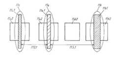
図6を用いて、第六の実施の形態を説明する。図6は、本発明の第六の実施の形態の半導体集積回路のレイアウトパターンの簡略図である。ゲート6a1と拡散領域6a2によって形成された活性トランジスタ6a、ゲート6b1と拡散領域6b2によって形成されたトランジスタ6b、ゲート6c1が、活性トランジスタ6aを中心に、その両側に配置され、活性トランジスタ6aとトランジスタ6bの間に、ダミーゲート6d1がゲート6a1と平行に配置されている。更に、活性トランジスタ6aとトランジスタ6bの間に、ゲート6f1と拡散領域6a2によって形成された非活性トランジスタ6fが配置されている。このように配置することにより、第四の実施の形態で述べたような効果に加え、活性トランジスタ6aのゲート6a1に対するフィンガー長が大きくなるので、活性トランジスタ6aの特性変動を抑制することができる。以下にその理由を詳しく述べる。(Sixth embodiment)
The sixth embodiment will be described with reference to FIG. FIG. 6 is a simplified diagram of the layout pattern of the semiconductor integrated circuit according to the sixth embodiment of the present invention. The active transistor 6a formed by the gate 6a1 and the diffusion region 6a2, the transistor 6b formed by the gate 6b1 and the diffusion region 6b2, and the gate 6c1 are disposed on both sides of the active transistor 6a, and the active transistor 6a and the transistor 6b. In between, the dummy gate 6d1 is arranged in parallel with the gate 6a1. Further, an
一般にSTI ストレスと呼ばれる活性領域とSTI 分離領域の熱膨張係数の違いにより、熱処理工程の際に生じるストレスが存在する。活性領域のほうがSTI 分離領域に比べ熱膨張係数が大きいため、熱処理後、活性領域には圧縮応力が生じる。この圧縮応力によって、活性領域のバンドが変形し、チャネル電荷の移動度が変化することでトランジスタ特性が変化する。活性領域が小さい、特にチャネルの中心から活性領域端までの長さ(フィンガー長)が小さいトランジスタで特性の変動が大きくなる。従って、非活性トランジスタ6fを備えることにより、右方向へのフィンガー長が大きくなった活性トランジスタ6aの特性変動は抑制されることになる。なお、非活性トランジスタ6fは活性トランジスタ6aに比べると、トランジスタ6bの近くに配置されており、かつそのフィンガー長が小さくなっており、仕上がり寸法のばらつきの影響を受け、特性変動も大きくなるが、容量トランジスタやオフトランジスタといった非活性トランジスタであるため、回路の所望の機能を実現するのに寄与しないため、問題とならない。 Generally, there is a stress that occurs during the heat treatment process due to the difference in thermal expansion coefficient between the active region and the STI isolation region, which is called STI stress. Since the active region has a larger coefficient of thermal expansion than the STI isolation region, compressive stress is generated in the active region after heat treatment. Due to this compressive stress, the band of the active region is deformed, and the mobility of the channel charge changes, whereby the transistor characteristics change. Variations in characteristics increase with a transistor having a small active region, in particular, a small length (finger length) from the center of the channel to the end of the active region. Therefore, by providing the
なお、上記第六の実施の形態において、図6のゲート6a1,6b1, 6c1,ダミーゲート6d1,6f1のゲート長を等長とし、かつ等間隔の配置にすると、光近接効果によるゲートの仕上がり寸法ばらつきを更に抑制することが出来る。 In the sixth embodiment, when the gate lengths of the gates 6a1, 6b1, 6c1 and dummy gates 6d1, 6f1 in FIG. 6 are equal, and are arranged at equal intervals, the finished dimensions of the gate due to the optical proximity effect Variation can be further suppressed.
(第七の実施の形態)
図7を用いて第七の実施の形態を説明する。図7は、本発明の第七の実施の形態の半導体集積回路のレイアウトパターンの簡略図である。ゲート7a1と拡散領域7a2によって形成された活性トランジスタ7a、ゲート7b1と拡散領域7b2によって形成されたトランジスタ7b、ゲート7c1が、活性トランジスタ7aを中心に、その両側に配置され、活性トランジスタ7aとトランジスタ7bの間に、ダミーゲート7d1、7e1がゲート7a1と平行に配置されている。更に、ダミーゲート7d1とダミーゲート7e1の間に、ダミー拡散領域7g2が配置されている。このようにダミー拡散領域を配置することにより得られる効果に関して、以下で詳しく説明する。(Seventh embodiment)
A seventh embodiment will be described with reference to FIG. FIG. 7 is a simplified diagram of the layout pattern of the semiconductor integrated circuit according to the seventh embodiment of the present invention. The active transistor 7a formed by the gate 7a1 and the diffusion region 7a2, the transistor 7b formed by the gate 7b1 and the diffusion region 7b2, and the gate 7c1 are disposed on both sides of the active transistor 7a, and the active transistor 7a and the transistor 7b In between, dummy gates 7d1, 7e1 are arranged in parallel with the gate 7a1. Further, a dummy diffusion region 7g2 is disposed between the dummy gate 7d1 and the dummy gate 7e1. The effect obtained by arranging the dummy diffusion regions in this way will be described in detail below.
半導体集積回路は、成膜、フォトリソグラフィ、エッチング等により、回路パターンをシリコンウェハ上に形成することにより製造される。近年、半導体デバイスの高速化・高密度化を実現するために、回路パターンは微細化・多層化の方向に進んでいる。この結果、製造工程における回路パターンを形成したウェハ表面の凹凸は増大する傾向にある。このようなウェハ表面の凹凸は配線等の形成に不可欠な露光を困難とするため、ウェハ表面の平坦化が行われている。この平坦化プロセスとして、化学的および物理的作用により表面を研磨して平坦化を実現するCMP( Chemical Mechanical Polishing) が用いられる。しかし、単にCMP工程を導入するだけでは所望の平坦性が得られない場合がある。例えば、半導体集積回路内での局所的なパターンの密度の違いによって、研磨後の膜厚が局所的に異なることは良く知られている。これらの段差が大きい場合、完全に平坦化できずCMP後の膜厚にばらつきが生じてしまう場合がある。このようなばらつきが大きい場合は、不良の原因となる。このため、膜厚ばらつきの発生を防ぐために様々な手法が開発されており、その代表的な手法の一つがダミーパターン挿入方式である。このダミーパターン挿入方式は、ダミーパターンを設けることにより平坦化を実現する方法である。研磨後の膜厚のばらつきは、溝を形成した部分で絶縁膜成膜後に凹状になっていることが原因の一つである。そこで、成膜後に凹状となることを防ぐために、実際には素子としての役割を果たさないパターン(ダミーパターン) を設ける。これにより表面の段差をなくし、研磨後の平坦化を実現する。広い溝部にダミーパターンを設けることによってより平坦な加工が実現できる(特開2004-273962号公報参照)。 A semiconductor integrated circuit is manufactured by forming a circuit pattern on a silicon wafer by film formation, photolithography, etching, or the like. In recent years, in order to realize higher speed and higher density of semiconductor devices, circuit patterns have progressed in the direction of miniaturization and multilayering. As a result, the unevenness of the wafer surface on which the circuit pattern is formed in the manufacturing process tends to increase. Since such irregularities on the wafer surface make it difficult to perform exposure that is indispensable for the formation of wiring and the like, the wafer surface is flattened. As this planarization process, CMP (Chemical Mechanical Polishing) is used, which realizes planarization by polishing the surface by chemical and physical action. However, the desired flatness may not be obtained simply by introducing the CMP process. For example, it is well known that the film thickness after polishing differs locally due to the difference in local pattern density in the semiconductor integrated circuit. If these steps are large, the film cannot be completely flattened and the film thickness after CMP may vary. When such a variation is large, it causes a defect. For this reason, various methods have been developed to prevent the occurrence of film thickness variations, and one of the representative methods is a dummy pattern insertion method. This dummy pattern insertion method is a method of realizing flattening by providing a dummy pattern. One of the causes of the variation in film thickness after polishing is that the groove is formed in a concave shape after the insulating film is formed. Therefore, in order to prevent a concave shape after film formation, a pattern (dummy pattern) that does not actually serve as an element is provided. This eliminates a step on the surface and realizes flattening after polishing. Flatter processing can be realized by providing a dummy pattern in a wide groove (see Japanese Patent Application Laid-Open No. 2004-273962).
以上述べたようにダミー拡散領域を配置することにより、拡散領域のパターン密度の均一化を図ることができるため、CMPによる平坦化の際に発生する凹凸を抑制することができ、その結果、精度の高い露光プロセスが実現できる。 As described above, by arranging the dummy diffusion region, the pattern density of the diffusion region can be made uniform, so that unevenness that occurs during planarization by CMP can be suppressed, and as a result, accuracy High exposure process can be realized.
なお、上記第七の実施の形態で、ダミー拡散領域を配置したようにダミーメタル配線を配置すると、上記第七の実施の形態で述べた理由によりメタル配線のパターン密度を均一化することができる。 If the dummy metal wiring is arranged like the dummy diffusion region in the seventh embodiment, the pattern density of the metal wiring can be made uniform for the reason described in the seventh embodiment. .
また、上記第七の実施の形態において、ダミー拡散領域を配置したように基板コンタクト領域を配置すると、一般に基板コンタクトは拡散領域、コンタクト、メタル配線で形成されているため、上記第七の実施の形態で述べた理由により拡散領域とメタル領域のパターン密度が均一化出来ることに加え、さらには基板電位を安定させることができる。 In the seventh embodiment, when the substrate contact region is arranged like the dummy diffusion region, the substrate contact is generally formed of a diffusion region, a contact, and a metal wiring. For the reason described in the embodiment, the pattern density of the diffusion region and the metal region can be made uniform, and further, the substrate potential can be stabilized.
なお、第三から第七の実施の形態で、活性トランジスタとそれに隣接するトランジスタの間にダミーゲート、非活性トランジスタ、ダミー拡散領域、ダミーメタル領域、基板コンタクト領域などを配置してきたが、第七の実施の形態のように、これらの項目のうち数項目を同時併用することも可能である。 In the third to seventh embodiments, a dummy gate, an inactive transistor, a dummy diffusion region, a dummy metal region, a substrate contact region, and the like are arranged between the active transistor and the adjacent transistor. As in the embodiment, several of these items can be used simultaneously.
なお、第一から第七の実施の形態は、クロック信号を伝播する回路に用いることが望ましい。なぜならば、クロック信号を伝播している回路に含まれている活性トランジスタは、そのゲート寸法精度を特に高める必要があるからである。その理由について、以下で詳しく説明する。 The first to seventh embodiments are desirably used for circuits that propagate clock signals. This is because the active transistor included in the circuit propagating the clock signal needs to have particularly high gate dimensional accuracy. The reason will be described in detail below.
一般に、半導体集積回路を同期化するためにクロック信号が分配されて供給されている。従来、このクロック信号を多数のレジスタ等に小さなクロックスキューで分配するため、遅延素子や配線等によりその遅延を調整したり、さらにレジスタ等に至るまでのクロックを配送する回路の構成を全て統一することなどが行われている。 Generally, a clock signal is distributed and supplied to synchronize a semiconductor integrated circuit. Conventionally, since this clock signal is distributed to a large number of registers with a small clock skew, the delay is adjusted by delay elements, wiring, etc., and the configuration of the circuit that distributes the clocks up to the registers, etc. is unified. Things are being done.
現在の大規模化した半導体集積回路には多数のレジスタ等が含まれており、これら多数のレジスタ等にクロック信号を分配する必要があることから、クロックを分配する回路は数段のゲートにより構成されている。そのために、クロック分配回路を半導体集積回路内で統一した構造としても、半導体集積回路の製造上のばらつきによりクロック分配回路の遅延時間にばらつきを生じ、その結果、レジスタ等に分配されるクロック間にはクロックスキューが生じることになる。 The current large-scale semiconductor integrated circuit includes a large number of registers, and the clock signal needs to be distributed to the large number of registers. Therefore, the clock distribution circuit is composed of several stages of gates. Has been. Therefore, even if the clock distribution circuit is integrated in the semiconductor integrated circuit, the delay time of the clock distribution circuit varies due to manufacturing variations of the semiconductor integrated circuit, and as a result, between clocks distributed to registers and the like. Will cause clock skew.
特に、微細化プロセスにおいては、クロック周期が短くなり、かつ、製造上のばらつきが大きくなるため、クロック周期に占めるスキューの割合が大きくなり問題となっている。こうした背景から、クロック信号を伝播する回路においては、特にトランジスタのゲート寸法精度を高めたいという要求がある。なお、一般的には、クロック信号を伝播する回路は、インバータ回路やバッファ回路で構成されることが多い。 In particular, in the miniaturization process, the clock cycle is shortened and the manufacturing variation is increased, so that the ratio of the skew to the clock cycle is increased, which is a problem. From such a background, in a circuit that propagates a clock signal, there is a demand for improving the gate dimensional accuracy of a transistor. In general, a circuit that propagates a clock signal is often composed of an inverter circuit and a buffer circuit.
なお、言うまでもないが、クロック信号を伝播している回路のみでなく、高精度な信号伝播が要求される信号経路上に用いられる回路であればどこでも、上記第一から第七の実施の形態は有効である。 Needless to say, the first to seventh embodiments are not limited to circuits that propagate clock signals, but any circuits that are used on signal paths that require high-accuracy signal propagation. It is valid.
(第八の実施の形態)
図8を用いて、第八の実施の形態を説明する。図8は、本発明の第八の実施の形態の半導体集積回路のレイアウトパターンの簡略図である。ゲート8a1と拡散領域8a2によって形成された活性トランジスタ8a、ゲート8b1と拡散領域8b2によって形成されたトランジスタ8b、ゲート8c1と拡散領域8c2によって形成されたトランジスタ8cが、活性トランジスタ8aを中心に、その両側に配置されている。ここで、ゲート8a1とゲート8b1との間隔を8S1、ゲート8a1とゲート8c1との間隔を8S2とした場合、8S1が8S2より大きくなるように配置する。上記第一から第七の実施の形態に対して、第八の実施の形態の大きく異なる点は、ダミーゲート8d1が存在しない点である(図8にダミーゲート8d1は点線で記載しているが、これは理解を容易とするため記載したもので、ダミーゲート8d1は図8のレイアウトパターン上には存在しない)。(Eighth embodiment)
The eighth embodiment will be described with reference to FIG. FIG. 8 is a simplified diagram of the layout pattern of the semiconductor integrated circuit according to the eighth embodiment of the present invention. The active transistor 8a formed by the gate 8a1 and the diffusion region 8a2, the transistor 8b formed by the gate 8b1 and the diffusion region 8b2, and the transistor 8c formed by the gate 8c1 and the diffusion region 8c2 are centered on the active transistor 8a. Is arranged. Here, when the interval between the gate 8a1 and the gate 8b1 is 8S1, and the interval between the gate 8a1 and the gate 8c1 is 8S2, the gates 8a1 and 8b1 are arranged so that 8S1 is larger than 8S2. The eighth embodiment is greatly different from the first to seventh embodiments in that the dummy gate 8d1 does not exist (although the dummy gate 8d1 is indicated by a dotted line in FIG. 8). This is described for ease of understanding, and the dummy gate 8d1 does not exist on the layout pattern of FIG. 8).
第一から第七の実施の形態では、トランジスタのゲート間隔を広げ、かつ、これらのダミーゲートを用いてゲートを等間隔にすることでゲートの仕上がり寸法ばらつきを抑えるという手法であったが、上記第八の実施の形態は、ダミーゲートを用いず、トランジスタのゲート間隔を広げることによってのみ、ゲートの仕上がり寸法ばらつきを抑えるという手法である。本実施の形態のように間隔を広げてレイアウトすることで、トランジスタ8bのゲート8b1が活性トランジスタ8aのゲート8a1に与える光近接効果による仕上がり寸法ばらつきの影響を抑えることが出来る。 In the first to seventh embodiments, the gate spacing of the transistors is widened, and the gates are equally spaced using these dummy gates. The eighth embodiment is a technique of suppressing variations in the finished dimensions of the gate only by widening the gate spacing of the transistors without using a dummy gate. By widening the layout as in the present embodiment, it is possible to suppress the influence of the finished size variation due to the optical proximity effect that the gate 8b1 of the transistor 8b gives to the gate 8a1 of the active transistor 8a.
なお、上記第八の実施の形態において、ゲート8a1,8b1,8c1を等長にすると、光近接効果によるゲートの仕上がり寸法ばらつきを更に抑えることが出来る。 In the eighth embodiment, if the gates 8a1, 8b1, and 8c1 have the same length, it is possible to further suppress variations in the finished dimensions of the gate due to the optical proximity effect.
また、上記第八の実施の形態を用いるとゲート長の仕上がり寸法精度を高めることが出来るため、活性トランジスタ8aがクロック信号を伝播している回路に含まれている場合には特に有効である。その理由は、前述の実施の形態において既に説明しているためここでは省略する。 Further, when the eighth embodiment is used, it is possible to improve the finished dimensional accuracy of the gate length, which is particularly effective when the active transistor 8a is included in a circuit that propagates a clock signal. The reason is omitted here because it has already been described in the above embodiment.
(第九の実施の形態)
図9を用いて、第九の実施の形態を説明する。図9は、本発明の第九の実施の形態の半導体集積回路のレイアウトパターンの簡略図である。図8に対して図9が異なる点は、トランジスタ9bのゲート9b1のゲート長が、トランジスタ9aのゲート9a1及びトランジスタ9cのゲート9c1のゲート長よりも大きい点である。(Ninth embodiment)
The ninth embodiment will be described with reference to FIG. FIG. 9 is a simplified diagram of the layout pattern of the semiconductor integrated circuit according to the ninth embodiment of the present invention. 9 differs from FIG. 8 in that the gate length of the gate 9b1 of the transistor 9b is larger than the gate lengths of the gate 9a1 of the transistor 9a and the gate 9c1 of the transistor 9c.
このように9b1のゲート長を大きくすることで、第五の実施の形態で述べたように面積効率良く容量トランジスタを構成することができるが、近接するトランジスタのゲートに与える光近接効果による仕上がり寸法ばらつきへの影響が大きい。そこで、図8のゲート8a1とゲート8b1の間隔8S1よりも図9のゲート9a1とゲート9b1の間隔9S1を大きく取ることにより、トランジスタ9bのゲート9b1が活性トランジスタ9aのゲート9a1に与える光近接効果による仕上がり寸法ばらつきの影響を抑えることができる。 By increasing the gate length of 9b1 in this way, a capacitive transistor can be configured with area efficiency as described in the fifth embodiment, but the finished dimensions due to the optical proximity effect given to the gates of adjacent transistors Large impact on variation. Therefore, by making the distance 9S1 between the gate 9a1 and the gate 9b1 in FIG. 9 larger than the distance 8S1 between the gate 8a1 and the gate 8b1 in FIG. 8, the optical proximity effect that the gate 9b1 of the transistor 9b gives to the gate 9a1 of the active transistor 9a The influence of finished dimensional variation can be suppressed.
なお、上記第九の実施の形態において、ゲート長の大きいトランジスタとして容量トランジスタを挙げたが、それには限られない。 In the ninth embodiment, a capacitor transistor is described as a transistor having a large gate length. However, the present invention is not limited to this.
(第十の実施の形態)
図10を用いて、第十の実施の形態を説明する。図10は、本発明の第十の実施の形態の半導体集積回路のレイアウトパターンの簡略図である。ゲート10a1と拡散領域10a2によって形成された活性トランジスタ10a、ゲート10b1と拡散領域10b2によって形成されたトランジスタ10b、ゲート10c1と拡散領域10c2によって形成されたトランジスタ10cが、活性トランジスタ10aを中心に、その両側に配置され、活性トランジスタ10aとトランジスタ10bの間に、ゲート10d1と拡散領域10a2によって形成された活性トランジスタ10dが配置されている。(Tenth embodiment)
The tenth embodiment will be described with reference to FIG. FIG. 10 is a simplified diagram of the layout pattern of the semiconductor integrated circuit according to the tenth embodiment of the present invention. The
このように配置することにより、トランジスタ10bのゲート10b1が活性トランジスタ10aのゲート10a1に与える光近接効果による仕上がり寸法ばらつきの影響は、非活性トランジスタ10dがない場合よりも抑えることができ、更に、第十の実施の形態によれば、活性トランジスタ10aのゲート10a1に対するフィンガー長が大きくなるので、第六の実施の形態で説明した通り、活性トランジスタ10aの特性変動を抑制することができる。また、非活性トランジスタ10dの仕上がり寸法のばらつきや特性変動が大きくなることが問題とならないことも第六の実施の形態で説明した通りである。 With this arrangement, the influence of the finished size variation due to the optical proximity effect that the gate 10b1 of the
なお、上記第十の実施の形態において、ゲート10a1,10b1,10d1を等長にすると、光近接効果によるゲートの仕上がり寸法ばらつきを更に抑えることが出来る。 In the tenth embodiment, if the gates 10a1, 10b1, and 10d1 have the same length, variations in the finished dimensions of the gate due to the optical proximity effect can be further suppressed.
(第十一の実施の形態)
図11を用いて第十一の実施の形態を説明する。図11は、本発明の第十一の実施の形態の半導体集積回路のレイアウトパターンの簡略図である。ゲート11a1と拡散領域11a2によって形成された活性トランジスタ11a、ゲート11b1と拡散領域11b2によって形成されたトランジスタ11b、ゲート11c1と拡散領域11c2によって形成されたトランジスタ11cが、活性トランジスタ11aを中心に、その両側に配置され、活性トランジスタ11aとトランジスタ11bの間にダミー拡散領域11d2が配置されている。このようにダミー拡散領域を配置することにより、第七の実施の形態で述べたように、パターン密度の均一化を図ることができる。(Eleventh embodiment)
The eleventh embodiment will be described with reference to FIG. FIG. 11 is a simplified diagram of a layout pattern of the semiconductor integrated circuit according to the eleventh embodiment of the present invention. An
なお、上記第十一の実施の形態で、ダミー拡散領域を配置したようにダミーメタル配線を配置すると、上記第十一の実施の形態で述べた理由によりメタル配線のパターン密度を均一化することができる。 In the eleventh embodiment, when the dummy metal wiring is arranged like the dummy diffusion region, the pattern density of the metal wiring is made uniform for the reason described in the eleventh embodiment. Can do.
また、上記第十一の実施の形態において、ダミー拡散領域を配置したように基板コンタクト領域を配置すると、一般に基板コンタクトは拡散領域、コンタクト、メタル配線で形成されているため、上記第七の実施の形態で述べた理由により拡散領域とメタル領域のパターン密度が均一化出来ることに加え、さらには基板電位を安定させることができる。 In the eleventh embodiment, when the substrate contact region is arranged like the dummy diffusion region, the substrate contact is generally formed of a diffusion region, a contact, and a metal wiring. For the reason described in the above embodiment, the pattern density of the diffusion region and the metal region can be made uniform, and further, the substrate potential can be stabilized.
なお、第十一の実施の形態において、活性トランジスタ11aとトランジスタ11bの間には非活性トランジスタ、ダミー拡散領域、ダミーメタル領域、基板コンタクト領域などを配置してきたが、これらの項目のうち数項目を同時併用することも可能である。 In the eleventh embodiment, an inactive transistor, a dummy diffusion region, a dummy metal region, a substrate contact region, and the like have been arranged between the
(第十二の実施の形態)
一般的に、半導体集積回路のレイアウト設計は、標準セルを組み合わせて行われることが多い。標準セルとは、複数のトランジスタを組み合わせた基本的な機能を有するレイアウト設計等の基本単位となるものである。標準セル内にはトランジスタやダミーゲートなどが含まれている。標準セルの機能としてはインバータ、NAND、AND、NOR、OR、EXOR、ラッチ、フリップフロップなどがある。(Twelfth embodiment)
In general, the layout design of a semiconductor integrated circuit is often performed by combining standard cells. The standard cell is a basic unit for layout design or the like having a basic function of combining a plurality of transistors. The standard cell includes a transistor and a dummy gate. Standard cell functions include inverter, NAND, AND, NOR, OR, EXOR, latch, and flip-flop.
これまで第一から第十一までの実施の形態を通じて活性トランジスタのゲートとそれに近接するゲートを離して活性トランジスタの仕上がり寸法ばらつきを抑えることが出来る手法を説明してきたが、標準セルを用い自動配置ツールによってチップのレイアウト設計を行う場合には、標準セルをどのように並べて配置しても標準セルの両端に位置する活性トランジスタの仕上がり寸法ばらつきを抑えられるように、標準セルのレイアウト形状を考慮しておく必要がある。 So far, we have explained the method that can suppress the variation of the finished size of the active transistor by separating the gate of the active transistor and the gate adjacent to it through the first to eleventh embodiments. When designing the chip layout with a tool, consider the layout of the standard cell so that the variation in the finished dimensions of the active transistors at both ends of the standard cell can be suppressed no matter how the standard cells are arranged. It is necessary to keep.
すなわち、標準セルのレイアウト設計を行う場合、標準セル内の両端に位置する活性トランジスタ以外に対しては上記実施の形態で述べたレイアウト形状にしておくことにより、トランジスタの仕上がり寸法ばらつきを抑えることが可能だが、標準セル内の両端に位置する活性トランジスタに対しては、その標準セルに隣接してどのような標準セルが配置されるかは分からないため、どのような標準セルが隣接して配置されようとも上記実施の形態で述べてきたレイアウト形状が形成されるように予め考慮して標準セルのレイアウト設計をしなければならない。 That is, when designing the layout of a standard cell, variations in the finished dimensions of the transistors can be suppressed by using the layout shape described in the above embodiment for the active transistors located at both ends in the standard cell. It is possible, but for active transistors located at both ends in a standard cell, it is not known what standard cell is placed adjacent to the standard cell, so what standard cells are placed adjacent to each other. Even so, the layout design of the standard cell must be designed in advance so that the layout shape described in the above embodiment is formed.
図24に標準セルのレイアウト図の一例としてインバータのレイアウト図を示す。図24における標準セルはP+拡散領域2403とゲート2401からなるPチャネル型トランジスタおよびN+拡散領域2402とゲート2401からなるNチャネル型トランジスタを備えている。ゲート2401にはメタル配線である入力端子2407からの入力信号がコンタクト2404を介して供給されている。Pチャネルトランジスタにはメタル配線である電源配線2405からコンタクト2404を介してソース端子に電源電位が供給されている。Nチャネルトランジスタにはメタル配線である接地配線2406からコンタクト2404を介してソース端子に接地電位が供給されている。そして入力端子2407の入力信号が反転されてメタル配線である出力端子2408に出力される。 FIG. 24 shows an inverter layout diagram as an example of a standard cell layout diagram. The standard cell in FIG. 24 includes a P-channel transistor composed of a P +
なお、以下の標準セルの発明の実施例においては、説明の簡単化のため、メタル配線、コンタクト等については省略してある。 In the following embodiments of the invention of the standard cell, metal wiring, contacts, etc. are omitted for the sake of simplicity.
また、一般的に標準セルはPチャネルトランジスタおよびNチャネルトランジスタの2列のトランジスタ列を含んでいるが、以下の実施例においては説明の簡単化のために1列のトランジスタ列のみを記載している。しかし、本発明は下記の実施例に記載されてあるような1列のトランジスタ列の場合に限定されるものではなく、一般的な標準セルである2列のトランジスタ列を含む標準セルなどにも当然にして適用できるものである。 In general, a standard cell includes two transistor columns of a P-channel transistor and an N-channel transistor. However, in the following embodiments, only one transistor column is described for the sake of simplicity of explanation. Yes. However, the present invention is not limited to the case of a single transistor row as described in the following embodiment, but also to a standard cell including two rows of transistor rows, which is a general standard cell. Of course, it can be applied.
図12を用いて、第十二の実施の形態を説明する。図12は、本発明の第十二の実施の形態の標準セルのレイアウトパターンの簡略図である。図12には本発明に係る標準セル12hに対して標準セル12iが隣接配置されたレイアウトパターンの簡略図を記載している。標準セル12h, 12iはそれぞれのセル枠を接して配置されている。 A twelfth embodiment will be described with reference to FIG. FIG. 12 is a simplified diagram of a standard cell layout pattern according to the twelfth embodiment of the present invention. FIG. 12 is a simplified diagram of a layout pattern in which standard cells 12i are arranged adjacent to
ゲート12a1と拡散領域12a2によって形成された活性トランジスタ12aに対してゲート12c1が隣接配置され、ゲート12c1とは逆側に、ゲート12a1と12c1を含むセル枠の一辺が存在している。ここで、ゲート12a1とセル枠との間隔を12S1、ゲート12a1とゲート12c1との間隔を12S2とし、12S1が12S2より大きくなるようにゲートを配置する。このように配置することにより、活性トランジスタ12aのゲート12a1が隣接する標準セル12i内のゲート12b1がいかなる位置に配置されていたとしても、ゲート12a1とゲート12b1間の距離はゲート12a1とゲート12c1より大きくなり、従って、光近接効果によるゲート12a1の仕上がり寸法ばらつきの影響を抑えることが出来る。 A gate 12c1 is disposed adjacent to the active transistor 12a formed by the gate 12a1 and the diffusion region 12a2, and one side of the cell frame including the gates 12a1 and 12c1 exists on the opposite side of the gate 12c1. Here, the interval between the gate 12a1 and the cell frame is 12S1, the interval between the gate 12a1 and the gate 12c1 is 12S2, and the gates are arranged so that 12S1 is larger than 12S2. With this arrangement, the distance between the gate 12a1 and the gate 12c1 is greater than the distance between the gate 12a1 and the gate 12c1 regardless of the position of the gate 12b1 in the standard cell 12i adjacent to the gate 12a1 of the active transistor 12a. Accordingly, it is possible to suppress the influence of variations in the finished dimensions of the gate 12a1 due to the optical proximity effect.
なお、上記第十二の実施の形態において、第三の実施の形態で述べたように、ゲート12c1がトランジスタのゲートであってもダミーゲートであっても同様の効果を得ることができる。 In the twelfth embodiment, as described in the third embodiment, the same effect can be obtained regardless of whether the gate 12c1 is a transistor gate or a dummy gate.
(第十三の実施の形態)
図13を用いて、第十三の実施の形態を説明する。図13は、本発明の第十三の実施の形態の標準セルのレイアウトパターンの簡略図である。図12に対して図13が異なる点は、図13の活性トランジスタ13aと標準セル13hとの間及びセル枠上にダミーゲート13d1,13e1を配置した点である。ダミーゲート13e1は標準セル13hのセル枠上に配置されているとともに、標準セル13iのセル枠上にも設けられており、標準セル13h, 13iが隣接配置されたときに標準セル間でセル枠境界上で共有されている。(Thirteenth embodiment)
The thirteenth embodiment will be described with reference to FIG. FIG. 13 is a simplified diagram of a standard cell layout pattern according to the thirteenth embodiment of the present invention. FIG. 13 differs from FIG. 12 in that dummy gates 13d1 and 13e1 are arranged between the
これにより、標準セル13i内のゲート13b1がいかなる位置に配置されていたとしても、ダミーゲート13d1,13e1が存在しない場合よりも活性トランジスタ13aのゲート13a1が受ける光近接効果による仕上がり寸法ばらつきの影響を、抑える事が出来る。 As a result, regardless of the position of the gate 13b1 in the standard cell 13i, the effect of variations in the finished size due to the optical proximity effect received by the gate 13a1 of the
なお、上記第十三の実施の形態において、ゲート13a1,13c1,ダミーゲート13d1,13e1のゲート長を等長とし、かつ等間隔に配置にすると、光近接効果によるゲートの仕上がり寸法ばらつきを更に抑制することが出来る。 In the thirteenth embodiment, if the gate lengths of the gates 13a1 and 13c1 and the dummy gates 13d1 and 13e1 are equal and arranged at equal intervals, variations in the finished dimensions of the gate due to the optical proximity effect are further suppressed. I can do it.
(第十四の実施の形態)
図14を用いて、第十四の実施の形態を説明する。図14は、本発明の第十四の実施の形態の標準セルのレイアウトパターンの簡略図である。図13に対して図14が異なる点は、図13のダミーゲート13d1が図14ではゲート14d1は拡散領域14a2上で非活性トランジスタを構成している点である。これにより、上記第六及び第十の実施の形態で述べた通り、光近接効果によるゲートの仕上がり寸法ばらつき抑制に加え、第六の実施の形態で述べた理由により、活性トランジスタ14aのゲート14a1に対するフィンガー長が大きくなることに起因するSTIストレス緩和により活性トランジスタ14aの特性変動を抑制する事ができる。また、非活性トランジスタ14dの仕上がり寸法のばらつきや特性変動が大きくなることが問題とならないことも第六の実施の形態で説明した通りである。(14th embodiment)
The fourteenth embodiment will be described with reference to FIG. FIG. 14 is a simplified diagram of a standard cell layout pattern according to the fourteenth embodiment of the present invention. FIG. 14 differs from FIG. 13 in that the dummy gate 13d1 in FIG. 13 forms an inactive transistor on the diffusion region 14a2 in FIG. As a result, as described in the sixth and tenth embodiments, in addition to suppressing variation in the finished dimensions of the gate due to the optical proximity effect, for the reason described in the sixth embodiment, the gate 14a1 of the active transistor 14a The fluctuation of the characteristics of the active transistor 14a can be suppressed by alleviating the STI stress caused by the increase in the finger length. In addition, as described in the sixth embodiment, it is not a problem that variations in the finished dimensions and characteristic fluctuations of the
なお、上記第十四の実施の形態において、ゲート14a1,14c1,14d1,14e1のゲート長を等長とし、かつ等間隔に配置にすると、光近接効果によるゲートの仕上がり寸法ばらつきを更に抑制することが出来る。 In the fourteenth embodiment, if the gate lengths of the gates 14a1, 14c1, 14d1, and 14e1 are equal and arranged at equal intervals, it is possible to further suppress variations in the finished dimensions of the gate due to the optical proximity effect. I can do it.
(第十五の実施の形態)
図15を用いて第十五の実施の形態を説明する。図15は、本発明の第十五の実施の形態の標準セルのレイアウトパターンの簡略図である。図13に対して図15が異なる点は、ダミーゲート15d1と15e1間の領域にかかるようにして自動配置配線時の端子アクセス領域となる端子領域15kが配置されていることである。(Fifteenth embodiment)
The fifteenth embodiment will be described with reference to FIG. FIG. 15 is a simplified diagram of a standard cell layout pattern according to the fifteenth embodiment of the present invention. FIG. 15 differs from FIG. 13 in that a
本実施の形態とは異なりセル端の活性トランジスタとセル枠との間隔を広げない場合はダミーゲート15d1と15e1の間の空き領域は存在しないため、端子領域15kはダミーゲート15d1よりもセル内側に配置しなければならない。なぜならば、端子領域15kがセル枠からはみ出して配置されていると、標準セルが隣接した際に隣接する標準セルの端子領域と短絡する恐れがあるためである。端子領域を標準セル内部に配置しなければならなくなると端子領域が標準セル内部で密集する、あるいは端子領域を配置するスペースが不十分なため端子領域を縮小せざるを得なくなるので、自動配線時の配線アクセス性が悪くなる。 Unlike this embodiment, if the gap between the active transistor at the cell edge and the cell frame is not widened, there is no empty area between the dummy gates 15d1 and 15e1, so the
この実施の形態のようにセル端の活性トランジスタとセル枠との間隔を広げた領域を利用して端子領域を広げて配置することにより端子領域の混雑度が緩和でき、また、十分な端子領域を確保することが出来るため、自動配線時の配線アクセス性が向上する。 As in this embodiment, the terminal region is widened by using the region where the gap between the active transistor at the cell edge and the cell frame is widened, thereby reducing the degree of congestion of the terminal region, and sufficient terminal region. Therefore, wiring accessibility during automatic wiring is improved.
なお、第十五の実施の形態において、セル内端子領域15kはゲート伸長方向に対して垂直に伸長する場合を述べたが、ゲート伸長方向に対して平行に伸長する場合にも同様に有効である。 In the fifteenth embodiment, the case where the in-
また、第十五の実施の形態において、セル内端子領域15kを伸長することで上記端子領域15kを形成する配線層とその直下の配線層との間のコンタクトに対してのメタル配線のカバー率をあげることができ、場合によってはコンタクト数を増加することが出来るので、プロセス形成時のコンタクト不良による動作不具合の発生率を抑えることにもつながる。 Further, in the fifteenth embodiment, the coverage ratio of the metal wiring with respect to the contact between the wiring layer forming the
なお、第十三から第十五の実施の形態では、セル枠とセル枠に最近接配置されている活性トランジスタの間の空き領域にダミーゲート、非活性トランジスタ、セル内端子領域、コンタクトを配置したが、第七の実施の形態で前述した通り、ダミー拡散領域、ダミーメタル領域、基板コンタクト領域を設けることも可能で、更に、それらのうちの数項目を同時併用することも可能である。その効果は第七の実施の形態で述べた通りである。 In the thirteenth to fifteenth embodiments, a dummy gate, an inactive transistor, an in-cell terminal region, and a contact are arranged in the empty area between the cell frame and the active transistor arranged closest to the cell frame. However, as described above in the seventh embodiment, it is possible to provide a dummy diffusion region, a dummy metal region, and a substrate contact region, and it is also possible to use several of them simultaneously. The effect is as described in the seventh embodiment.
なお、上記第十三から第十五の実施の形態のようなレイアウトを施した標準セルは、クロック信号を伝播している回路に有効である。その理由は、第七の実施の形態において既に説明しているためここでは省略する。 The standard cell having the layout as in the thirteenth to fifteenth embodiments is effective for a circuit that propagates a clock signal. The reason is omitted here because it has already been described in the seventh embodiment.
なお、第十二から第十五までの実施の形態では、セル端の片側についてしか説明していないが、逆側のセル端についても同様のレイアウト形状にした方が望ましい。なぜなら、標準セルは自動配置時に左右に連続して隣接して配置され、さらには標準セルは左右反転させて配置される場合があるため、セルの片端だけ上記実施の形態を適用していても、適用されていないセル端には上記実施の形態で述べたような効果が得られないためである。また、セル列の端に位置した標準セルに対しては、何が隣接配置されるかわからないためでもある。 In the twelfth to fifteenth embodiments, only one side of the cell edge has been described. However, it is desirable that the opposite cell edge has a similar layout shape. This is because the standard cell may be arranged continuously adjacent to the left and right during automatic placement, and further, the standard cell may be placed upside down, so even if the above embodiment is applied to only one end of the cell. This is because the effect as described in the above embodiment cannot be obtained at a cell edge that is not applied. This is also because the standard cell located at the end of the cell row is not known to be adjacent.
(第十六の実施の形態)
図16を用いて、第十六の実施の形態を説明する。図16は、本発明の第十六の実施の形態の標準セルのレイアウトパターンの簡略図である。図16には本発明に係る標準セル16hに対して標準セル16iが隣接配置されたレイアウトパターンの簡略図を記載している。標準セル16h, 16iはそれぞれのセル枠を接して配置されている。(Sixteenth embodiment)
The sixteenth embodiment will be described with reference to FIG. FIG. 16 is a simplified diagram of a standard cell layout pattern according to the sixteenth embodiment of the present invention. FIG. 16 shows a simplified diagram of a layout pattern in which standard cells 16i are arranged adjacent to
ゲート16a1と拡散領域16a2によって形成された活性トランジスタ16aに対してゲート16c1と拡散領域16c2によって形成されたトランジスタ16cが隣接配置され、ゲート16a1に対してゲート16c1とは逆側に、ゲート16a1と16c1を含む標準セル16hのセル枠の一辺が存在している。ここで、ゲート16a1とセル枠との間隔を16S1、ゲート16a1とゲート16c1との間隔を16S2とし、16S1が16S2より大きくなるようにゲートを配置する。このように配置することにより、活性トランジスタ16aのゲート16a1が隣接する標準セル16i内のゲート16b1がいかなる位置に配置されていたとしても、ゲート16a1とゲート16b1間の距離はゲート16a1とゲート16c1より大きくなり、従って、光近接効果によるゲート16a1の仕上がり寸法ばらつきの影響を抑えることが出来る。 The
なお、上記第十六の実施の形態において、16S1が16S2より大きくなるようにゲートを配置するとしたが、16S1が16S2の半分より大きければよい。全ての標準セルに対してこのような基準をもって設計しておけば結果的にどのような標準セルが隣接した場合にもゲート16a1と隣接する標準セル内のゲート16b1との距離は16S2より大きくなるため同様の効果を得ることができるためである。 In the sixteenth embodiment, the gate is arranged so that 16S1 is larger than 16S2. However, 16S1 only needs to be larger than half of 16S2. If all the standard cells are designed with such a standard, the distance between the gate 16a1 and the gate 16b1 in the adjacent standard cell will be larger than 16S2 as a result of any standard cell adjoining. This is because the same effect can be obtained.
なお、上記第十六の実施の形態において、ゲート16a1,16c1のゲート長を等長とすると、光近接効果によるゲートの仕上がり寸法ばらつきを更に抑制することが出来る。 In the sixteenth embodiment, if the gate lengths of the gates 16a1 and 16c1 are equal, variations in the finished dimensions of the gate due to the optical proximity effect can be further suppressed.
(第十七の実施の形態)
図17を用いて、第十七の実施の形態を紹介する。図17は、本発明の第十七の実施の形態の標準セルのレイアウトパターンの簡略図である。図16に対して図17が異なる点は、活性トランジスタ17aと活性トランジスタ17aに最近接するセル枠との間に非活性トランジスタ17dを配置している点である。これにより、上記第六及び第十の実施の形態で述べた通り、光近接効果によるゲートの仕上がり寸法ばらつき抑制に加え、第六の実施の形態で述べた理由により、活性トランジスタ17aのゲート17a1に対するフィンガー長が大きくなるので、活性トランジスタ17aの特性変動を抑制することができる。また、非活性トランジスタ17dの仕上がり寸法のばらつきや特性変動が大きくなることが問題とならないことも第六の実施の形態で説明した通りである。(Seventeenth embodiment)
The seventeenth embodiment will be introduced with reference to FIG. FIG. 17 is a simplified diagram of a standard cell layout pattern according to the seventeenth embodiment of the present invention. FIG. 17 differs from FIG. 16 in that an inactive transistor 17d is arranged between the
なお、第十六及び第十七の実施の形態では、セル枠とセル枠に最近接配置されている活性トランジスタの間の空き領域に非活性トランジスタを配置したが、第七の実施の形態及び第十五の実施の形態で前述した通り、ダミー拡散領域、ダミーメタル領域、基板コンタクト領域、セル内端子領域、コンタクトを設けることも可能で、更に、それらのうちの数項目を同時併用することも可能である。 In the sixteenth and seventeenth embodiments, the inactive transistor is arranged in the empty area between the cell frame and the active transistor arranged closest to the cell frame. As described in the fifteenth embodiment, it is possible to provide a dummy diffusion region, a dummy metal region, a substrate contact region, an in-cell terminal region, and a contact, and use several of them simultaneously. Is also possible.
なお、上記第十六及び第十七の実施の形態のようなレイアウトを施した標準セルは、クロック信号を伝播している回路に有効である。その理由は、前述の実施の形態において既に説明しているためここでは省略する。 The standard cell having the layout as in the sixteenth and seventeenth embodiments is effective for a circuit that propagates a clock signal. The reason is omitted here because it has already been described in the above embodiment.
なお、第十六から第十七までの実施の形態では、セル端の片側についてしか説明していないが、逆側のセル端についても同様のレイアウト形状にした方が望ましい。なぜなら、標準セルは自動配置時に左右に連続して隣接して配置され、さらには標準セルは左右反転させて配置される場合があるため、セルの片端だけ上記実施の形態を適用していても、適用されていないセル端には上記実施の形態で述べたような効果が得られないためである。また、セル列の端に位置した標準セルに対しては、何が隣接配置されるかわからないためでもある。 In the sixteenth to seventeenth embodiments, only one side of the cell edge has been described. However, it is desirable that the opposite cell edge has a similar layout shape. This is because the standard cell may be arranged continuously adjacent to the left and right during automatic placement, and further, the standard cell may be placed upside down, so even if the above embodiment is applied to only one end of the cell. This is because the effect as described in the above embodiment cannot be obtained at a cell edge that is not applied. This is also because the standard cell located at the end of the cell row is not known to be adjacent.
(第十八の実施の形態)
第十八の実施の形態について説明する。上記第十二から第十七の実施の形態のようなレイアウトを施した標準セルを有する標準セルライブラリを構成する。上記標準セルライブラリを用いて、半導体集積回路の設計を行うことにより、ゲート長の仕上がり寸法ばらつきを抑えた半導体集積回路を得ることができる。(Eighteenth embodiment)
The eighteenth embodiment will be described. A standard cell library having standard cells laid out as in the twelfth to seventeenth embodiments is constructed. By designing a semiconductor integrated circuit using the standard cell library, it is possible to obtain a semiconductor integrated circuit in which variations in finished dimensions of the gate length are suppressed.
(第十九の実施の形態)
第十九の実施の形態について説明する。上記第十二から第十七の実施の形態のようなレイアウトを施した標準セルを使用して半導体集積回路を構成する。これによって、ゲート長の仕上がり寸法ばらつきを抑えた半導体集積回路を得ることができる。(Nineteenth embodiment)
The nineteenth embodiment will be described. A semiconductor integrated circuit is configured using standard cells having a layout as in the twelfth to seventeenth embodiments. As a result, it is possible to obtain a semiconductor integrated circuit in which variations in finished dimensions of the gate length are suppressed.
(第二十の実施の形態)
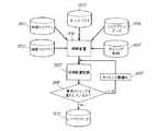
図18、図19を用いて、第二十の実施の形態を説明する。まず、図18を用いて、標準セルを配置し、標準セルの端子間の配線を行う自動配置配線ツールを用いた一般的な設計フローの概要を説明する。(20th embodiment)
The twentieth embodiment will be described with reference to FIGS. First, an outline of a general design flow using an automatic placement and routing tool that places standard cells and performs wiring between terminals of the standard cells will be described with reference to FIG.
図18において、物理ライブラリ1801と、論理ライブラリ1802と、標準セルライブラリを用いて記述された標準セル間の接続を記述したネットリスト1803と、配置可能領域を示すフロアプランデータ1804と、回路の動作タイミングを規定するタイミング制約1805を入力とし、概略配置工程1806と、詳細配置配線工程1807と、タイミング判定工程1808と、タイミング最適化工程1809を備える。物理ライブラリ1801は標準セルの信号端子などの物理形状のほかに、標準セル同士の重なりを制御するセル境界を備え、論理ライブラリ1802には標準セルの動作の記述のほかにトランジスタの種類を区別する属性情報をもつ。ネットリスト1803を構成する各標準セルはタイミング制約1805から得られるタイミング情報とフロアプランデータ1804から得られる混雑度を考慮しながら概略配置工程1806においてその概略の配置を得る。その後、詳細配置配線工程1807において、詳細な配置および標準セル間の配線を実施し、最終的な半導体集積回路のレイアウトデータ1810を得る。詳細配置配線工程1807完了後にタイミング判定工程1808で要求タイミングを満たしているかを確認し、満たしていない場合はタイミング最適化工程1809においてセルの移動や置換、再配線によりタイミング改善を行い、詳細配置配線工程1807を繰り返す。 In FIG. 18, the
次に、図19に示す第二十の実施の形態の本発明の半導体集積回路の設計方法のフロー図を説明する。標準セル配置工程1901において活性トランジスタを含む標準セルを配置し、スペーサー標準セル配置工程1902において、標準セルのうち指定される標準セルの両隣に隣接して活性トランジスタを含まない主にセル間のスペースを広げることを目的とするスペーサー標準セルを配置する。ここで、指定される標準セルとして、容量トランジスタのようにゲート長の大きいトランジスタをそのセル端に含む標準セルを指定しておけば、その両隣には、スペーサー標準セルが配置されることになる。このため、ゲート長が大きいトランジスタが周囲のゲートに与える光近接効果の増大を緩和することができ、スペーサー標準セルに対してゲート長の大きいトランジスタをそのセル単に含む標準セルとは反対側に配置される標準セルのゲート長のばらつきを抑制することができる。 Next, a flow diagram of a method for designing a semiconductor integrated circuit according to the twentieth embodiment of the present invention shown in FIG. 19 will be described. In the standard
なお、前記の指定される標準セルには、クロック信号を伝播する標準セルを選択してもよい。クロック信号を伝播する標準セルに隣接してスペーサー標準セルを配置することで、クロック信号を伝播する標準セルが隣接する標準セルに含まれるトランジスタによって受ける光近接効果の影響を低減することができ、クロック信号を伝播する標準セルのゲート長のばらつきを抑制することができる。特にクロック信号を伝播する標準セルに隣接したゲート長の大きい標準セルによる光近接効果の影響を緩和することに効果が大きい。 Note that a standard cell that propagates a clock signal may be selected as the designated standard cell. By placing the spacer standard cell adjacent to the standard cell that propagates the clock signal, the influence of the optical proximity effect that the standard cell that propagates the clock signal receives by the transistor included in the adjacent standard cell can be reduced. Variations in the gate length of the standard cell that propagates the clock signal can be suppressed. This is particularly effective in reducing the influence of the optical proximity effect caused by the standard cell having a large gate length adjacent to the standard cell that propagates the clock signal.
また、セル列の両端に配置された標準セルにおいては、片側には標準セルが配置されるものの、もう一方の側には標準セルが何も配置されないことになるため、セル列の両端に配置された標準セルを前記の指定される標準セルに選択しておけばセル列の両端に配置された標準セルに対する光近接効果の影響を緩和できる。 In the standard cell placed at both ends of the cell column, the standard cell is placed on one side, but no standard cell is placed on the other side. If the designated standard cell is selected as the designated standard cell, the influence of the optical proximity effect on the standard cells arranged at both ends of the cell row can be reduced.
なお、図19に示す工程は、図18でいえば、概略配置工程1806あるいは詳細配置配線工程1807に含まれることが望ましい。 Note that the step shown in FIG. 19 is preferably included in the general arrangement step 1806 or the detailed
なお、たとえば図19に示す工程を図18の概略配置工程に含ませた場合を考えた場合、物理ライブラリ1801、論理ライブラリ1802、ネットリスト1803、フロアプランデータ1804、タイミング制約1805、レイアウトデータ1810をハードディスクなどの記憶装置に記憶させて、そこからデータの入出力を行い、概略配置工程1806、詳細配置配線工程1807、タイミング判定工程1808、タイミング最適化工程1809、標準セル配置工程1901、スペーサー標準セル配置工程1902をCPUなどにおいて演算処理を行わせ、ユーザーはキーボードなどを使用してでスペーサー標準セルを隣接して配置する標準セルを指定するなどを行い、かつモニター画面などを通じて設計の途中段階のデータを確認や、レイアウトデータ1810の確認などをすることができ、本発明がハードウェア上で実現できることは言うまでもない。これは第二十一の実施の形態においても同様である。 For example, if the process shown in FIG. 19 is included in the schematic arrangement process of FIG. 18, the
(第二十一の実施の形態)
図20、図21を用いて第二十一の実施の形態を説明する。図20はスペーサー標準セルを模式的に表した図である。スペーサー標準セルを配置する主な目的は、光近接効果の影響を緩和するべく、標準セル間の間隔を広げることにあるため、スペーサー標準セル内には特に素子を配置する必要性は無いが、光近接効果に悪影響を与えない範囲でスペーサー標準セル内の空き領域を有効利用することも可能である。図21にダミー拡散領域を有するようにしたスペーサー標準セルを示す。図21のようにすることで、本来スペーサー標準セルに期待していたゲート長のばらつきを抑制する効果に加えて、拡散領域のパターン密度を均一化する効果も得られる。なお、スペーサー標準セル内には、非活性トランジスタ、ダミーゲート、ダイオード、ダミーメタル配線を配置することも同様に可能である。これらを配置することにより得られる効果及び理由は、前述の実施の形態において既に説明しているためここでは省略する。(21st embodiment)
The twenty-first embodiment will be described with reference to FIGS. FIG. 20 is a diagram schematically showing a spacer standard cell. The main purpose of placing the spacer standard cell is to widen the spacing between the standard cells in order to mitigate the effects of the optical proximity effect, so there is no need to place any elements in the spacer standard cell. It is also possible to effectively use the empty area in the spacer standard cell within a range that does not adversely affect the optical proximity effect. FIG. 21 shows a spacer standard cell having a dummy diffusion region. By doing as shown in FIG. 21, in addition to the effect of suppressing the variation of the gate length originally expected for the spacer standard cell, the effect of making the pattern density of the diffusion region uniform can also be obtained. It is also possible to dispose an inactive transistor, a dummy gate, a diode, and a dummy metal wiring in the spacer standard cell. The effects and reasons that can be obtained by arranging them have already been described in the above-described embodiment, and are omitted here.
本発明にかかる半導体集積回路等は、各種電子機器に搭載される半導体集積回路等に利用することができる。 The semiconductor integrated circuit according to the present invention can be used for a semiconductor integrated circuit mounted on various electronic devices.
1a1,1b1,1c1,2a1,2b1,2c1,3a1,3b1,3c1,4a1,4b1,4c1,5a1,5b1,5c1,6a1,6b1,6f1,7a1,7b1,7c1,8a1,8b1,8c1,9a1,9b1,9c1,10a1,10b1,10c1,10d1,11a1,11b1,11c1,12a1,12b1,12c1,13a1,13b1,13c1,14a1,14b1,14c1,14d1,15a1,15b1,15c1,16a1,16b1,16c1,17a1,17b1,17c1,17d1,L1,L2 ゲート
3d1,4d1,4e1,5d1,5e1,6c1,6d1,7d1,7e1,13d1,13e1,14e1,15d1,15e1 ダミーゲート
1a2,1b2,2a2,2b2,3a2,3b2,4a2,4b2,5a2,5b2,6a2,6b2,7a2,7b2,8a2,8b2,8c2,9a2,9b2,9c2,10a2,10b2,10c2,11a2,11b2,11c2,12a2,12b2,13a2,13b2,14a2,14b2,15a2,15b2,16a2,16b2, 16c2,17a2,17b2,17c2 拡散領域
1a,2a,3a,4a,5a,6a,7a,8a,9a,10a,11a,12a,13a,14a,15a,16a,17a 活性トランジスタ
1b,2b,3b,4b,5b,6b,7b,8b,8c,9b,9c,10b,10c,10d,11b,11c,12b,12c,13b,13c,14b,14c,15b,15c,16b,16c,17b,17c トランジスタ
6f,14d,17d 非活性トランジスタ
1S1,1S2,2S1,2S2,3S1,3S2,4S1,4S2,5S1,5S2,6S1,6S2,7S1,7S2,8S1,8S2,9S1,9S2,10S1,10S2,11S1,11S2,12S2,13S2,14S2,15S2,16S2,17S2,S ゲート間の距離
12S1,13S1,14S1,15S1,16S1,17S1 ゲートとセル枠の距離
7g2,11d2 ダミー拡散領域
12h,12i,13h,13i,14h,14i,15h,15i,16h,16i,17h,17i 標準セル
15k セル内端子領域
1801 物理ライブラリ
1802 論理ライブラリ
1803 ネットリスト
1804 フロアプランデータ
1805 タイミング制約
1806 概略配置工程
1807 詳細配置配線工程
1808 タイミング判定工程
1809 タイミング最適化工程
1810 レイアウトデータ
1901 標準セル配置工程
1902 スペーサー標準セル配置工程
2001,2101 スペーサー標準セル
2102 ダミー拡散領域
2401 ゲート
2402 N+拡散領域
2403 P+拡散領域
2404 コンタクト
2405 電源配線
2406 接地配線
2407 入力端子
2408 出力端子
2409 セル枠1a1,1b1,1c1,2a1,2b1,2c1,3a1,3b1,3c1,4a1,4b1,4c1,5a1,5b1,5c1,6a1,6b1,6f1,7a1,7b1,7c1,8a1,8b1,8c1,9a1, 9b1,9c1,10a1,10b1,10c1,10d1,11a1,11b1,11c1,12a1,12b1,12c1,13a1,13b1,13c1,14a1,14b1,14c1,14d1,15a1,15b1,15c1,16a1,16b1,16c1, 17a1,17b1,17c1,17d1, L1, L2 gate
3d1,4d1,4e1,5d1,5e1,6c1,6d1,7d1,7e1,13d1,13e1,14e1,15d1,15e1 Dummy gate
1a2,1b2,2a2,2b2,3a2,3b2,4a2,4b2,5a2,5b2,6a2,6b2,7a2,7b2,8a2,8b2,8c2,9a2,9b2,9c2,10a2,10b2,10c2,11a2,11b2, 11c2,12a2,12b2,13a2,13b2,14a2,14b2,15a2,15b2,16a2,16b2, 16c2,17a2,17b2,17c2 Diffusion region
1a, 2a, 3a, 4a, 5a, 6a, 7a, 8a, 9a, 10a, 11a, 12a, 13a, 14a, 15a, 16a, 17a Active transistor
1b, 2b, 3b, 4b, 5b, 6b, 7b, 8b, 8c, 9b, 9c, 10b, 10c, 10d, 11b, 11c, 12b, 12c, 13b, 13c, 14b, 14c, 15b, 15c, 16b, 16c, 17b, 17c transistor
6f, 14d, 17d Inactive transistor
1S1,1S2,2S1,2S2,3S1,3S2,4S1,4S2,5S1,5S2,6S1,6S2,7S1,7S2,8S1,8S2,9S1,9S2,10S1,10S2,11S1,11S2,12S2,13S2,14S2, 15S2,16S2,17S2, S Distance between gates
12S1,13S1,14S1,15S1,16S1,17S1 Distance between gate and cell frame
7g2,11d2 Dummy diffusion region
12h, 12i, 13h, 13i, 14h, 14i, 15h, 15i, 16h, 16i, 17h, 17i Standard cell
15k terminal area in a cell
1801 physical library
1802 Logical library
1803 Netlist
1804 Floor plan data
1805 Timing constraints
1806 General arrangement process
1807 Detailed placement and routing process
1808 Timing judgment process
1809 Timing optimization process
1810 Layout data
1901 Standard cell placement process
1902 Spacer standard cell placement process
2001,2101 Spacer standard cell
2102 Dummy diffusion area
2401 gate
2402 N + diffusion region
2403 P + diffusion region
2404 contacts
2405 Power supply wiring
2406 Ground wiring
2407 Input terminal
2408 Output terminal
2409 cell border
Claims (87)
Translated fromJapanesePriority Applications (5)
| Application Number | Priority Date | Filing Date | Title |
|---|---|---|---|
| JP2005191433AJP2007012855A (en) | 2005-06-30 | 2005-06-30 | Semiconductor integrated circuit, standard cell, standard cell library, semiconductor integrated circuit design method, and semiconductor integrated circuit design apparatus |
| US11/476,124US7685551B2 (en) | 2005-06-30 | 2006-06-28 | Semiconductor integrated circuit, standard cell, standard cell library, semiconductor integrated circuit designing method, and semiconductor integrated circuit designing equipment |
| CNB2006101005027ACN100521204C (en) | 2005-06-30 | 2006-06-30 | Semiconductor integrated circuit, standard cell library, design method, and design device |
| CN2008101499083ACN101393911B (en) | 2005-06-30 | 2006-06-30 | Semiconductor integrated circuit |
| US12/714,819US8261225B2 (en) | 2005-06-30 | 2010-03-01 | Semiconductor integrated circuit, standard cell, standard cell library, semiconductor integrated circuit designing method, and semiconductor integrated circuit designing equipment |
Applications Claiming Priority (1)
| Application Number | Priority Date | Filing Date | Title |
|---|---|---|---|
| JP2005191433AJP2007012855A (en) | 2005-06-30 | 2005-06-30 | Semiconductor integrated circuit, standard cell, standard cell library, semiconductor integrated circuit design method, and semiconductor integrated circuit design apparatus |
Publications (1)
| Publication Number | Publication Date |
|---|---|
| JP2007012855Atrue JP2007012855A (en) | 2007-01-18 |
Family
ID=37590127
Family Applications (1)
| Application Number | Title | Priority Date | Filing Date |
|---|---|---|---|
| JP2005191433APendingJP2007012855A (en) | 2005-06-30 | 2005-06-30 | Semiconductor integrated circuit, standard cell, standard cell library, semiconductor integrated circuit design method, and semiconductor integrated circuit design apparatus |
Country Status (3)
| Country | Link |
|---|---|
| US (2) | US7685551B2 (en) |
| JP (1) | JP2007012855A (en) |
| CN (2) | CN101393911B (en) |
Cited By (28)
| Publication number | Priority date | Publication date | Assignee | Title |
|---|---|---|---|---|
| JP2008249872A (en)* | 2007-03-29 | 2008-10-16 | Fujitsu Microelectronics Ltd | Mask pattern correction method and semiconductor device manufacturing method |
| JP2009021482A (en)* | 2007-07-13 | 2009-01-29 | Nec Electronics Corp | Automatic layout device of semiconductor integrated circuit and program |
| WO2010001506A1 (en)* | 2008-07-04 | 2010-01-07 | パナソニック株式会社 | Semiconductor integrated circuit device |
| JP2010021469A (en)* | 2008-07-14 | 2010-01-28 | Nec Electronics Corp | Semiconductor integrated circuit |
| US7800140B2 (en) | 2007-03-16 | 2010-09-21 | Panasonic Corporation | Semiconductor integrated circuit |
| WO2011048737A1 (en)* | 2009-10-19 | 2011-04-28 | パナソニック株式会社 | Semiconductor device |
| US7961010B2 (en) | 2009-01-19 | 2011-06-14 | Samsung Electronics Co., Ltd. | Dynamic logic circuit including dynamic standard cell library |
| WO2011077664A1 (en)* | 2009-12-25 | 2011-06-30 | パナソニック株式会社 | Semiconductor device |
| JP2013535836A (en)* | 2010-08-06 | 2013-09-12 | アルテラ コーポレイション | N-well / P-well strap structure |
| US8669596B2 (en) | 2010-03-05 | 2014-03-11 | Panasonic Corporation | Semiconductor device |
| KR20150016564A (en)* | 2007-10-26 | 2015-02-12 | 텔라 이노베이션스, 인코포레이티드 | Methods, structures and designs for self-aligning local interconnects used in integrated circuits |
| WO2015025441A1 (en)* | 2013-08-23 | 2015-02-26 | パナソニック株式会社 | Semiconductor integrated circuit device |
| US9202779B2 (en) | 2008-01-31 | 2015-12-01 | Tela Innovations, Inc. | Enforcement of semiconductor structure regularity for localized transistors and interconnect |
| US9208279B2 (en) | 2008-03-13 | 2015-12-08 | Tela Innovations, Inc. | Semiconductor chip including digital logic circuit including linear-shaped conductive structures having electrical connection areas located within inner region between transistors of different type and associated methods |
| US9230910B2 (en) | 2006-03-09 | 2016-01-05 | Tela Innovations, Inc. | Oversized contacts and vias in layout defined by linearly constrained topology |
| US9269702B2 (en) | 2009-10-13 | 2016-02-23 | Tela Innovations, Inc. | Methods for cell boundary encroachment and layouts implementing the same |
| US9281371B2 (en) | 2007-12-13 | 2016-03-08 | Tela Innovations, Inc. | Super-self-aligned contacts and method for making the same |
| US9336344B2 (en) | 2006-03-09 | 2016-05-10 | Tela Innovations, Inc. | Coarse grid design methods and structures |
| US9390215B2 (en) | 2008-03-27 | 2016-07-12 | Tela Innovations, Inc. | Methods for multi-wire routing and apparatus implementing same |
| US9425272B2 (en) | 2006-03-09 | 2016-08-23 | Tela Innovations, Inc. | Semiconductor chip including integrated circuit including four transistors of first transistor type and four transistors of second transistor type with electrical connections between various transistors and methods for manufacturing the same |
| US9424387B2 (en) | 2007-03-07 | 2016-08-23 | Tela Innovations, Inc. | Methods for cell phasing and placement in dynamic array architecture and implementation of the same |
| US9563733B2 (en) | 2009-05-06 | 2017-02-07 | Tela Innovations, Inc. | Cell circuit and layout with linear finfet structures |
| US9589091B2 (en) | 2006-03-09 | 2017-03-07 | Tela Innovations, Inc. | Scalable meta-data objects |
| US9595515B2 (en) | 2007-03-07 | 2017-03-14 | Tela Innovations, Inc. | Semiconductor chip including integrated circuit defined within dynamic array section |
| US9633987B2 (en) | 2007-03-05 | 2017-04-25 | Tela Innovations, Inc. | Integrated circuit cell library for multiple patterning |
| US9673825B2 (en) | 2006-03-09 | 2017-06-06 | Tela Innovations, Inc. | Circuitry and layouts for XOR and XNOR logic |
| US9704845B2 (en) | 2010-11-12 | 2017-07-11 | Tela Innovations, Inc. | Methods for linewidth modification and apparatus implementing the same |
| US9754878B2 (en) | 2006-03-09 | 2017-09-05 | Tela Innovations, Inc. | Semiconductor chip including a chip level based on a layout that includes both regular and irregular wires |
Families Citing this family (29)
| Publication number | Priority date | Publication date | Assignee | Title |
|---|---|---|---|---|
| JP2007311491A (en)* | 2006-05-17 | 2007-11-29 | Toshiba Corp | Semiconductor integrated circuit |
| KR100808605B1 (en)* | 2007-05-31 | 2008-02-29 | 주식회사 하이닉스반도체 | Semiconductor device in the peripheral circuit area |
| JP2008311361A (en)* | 2007-06-13 | 2008-12-25 | Nec Electronics Corp | Semiconductor integrated circuit, layout design method of semiconductor integrated circuit, and automatic layout program of semiconductor integrated circuit |
| KR101286644B1 (en)* | 2007-11-08 | 2013-07-22 | 삼성전자주식회사 | Semiconductor device including dummy gate part and method of fabricating thereof |
| CN101526967B (en)* | 2008-03-07 | 2011-08-03 | 北京芯慧同用微电子技术有限责任公司 | Design method and device for standard cell library |
| US8453100B2 (en)* | 2010-09-01 | 2013-05-28 | International Business Machines Corporation | Circuit analysis using transverse buckets |
| US8669775B2 (en)* | 2010-09-24 | 2014-03-11 | Texas Instruments Incorporated | Scribe line test modules for in-line monitoring of context dependent effects for ICs including MOS devices |
| US8661389B2 (en)* | 2011-04-12 | 2014-02-25 | Taiwan Semiconductor Manufacturing Company, Ltd. | Systems and methods of designing integrated circuits |
| US20120280354A1 (en)* | 2011-05-05 | 2012-11-08 | Synopsys, Inc. | Methods for fabricating high-density integrated circuit devices |
| US20130009250A1 (en)* | 2011-07-06 | 2013-01-10 | Mediatek Inc. | Dummy patterns for improving width dependent device mismatch in high-k metal gate process |
| US8635573B2 (en)* | 2011-08-01 | 2014-01-21 | Taiwan Semiconductor Manufacturing Company, Ltd. | Method of fabricating a semiconductor device having a defined minimum gate spacing between adjacent gate structures |
| JP6031086B2 (en)* | 2012-03-08 | 2016-11-24 | 株式会社ソシオネクスト | Semiconductor integrated circuit device |
| US8627243B1 (en)* | 2012-10-12 | 2014-01-07 | Taiwan Semiconductor Manufacturing Company, Ltd. | Methods for optimizing conductor patterns for ECP and CMP in semiconductor processing |
| US9209195B2 (en)* | 2013-05-01 | 2015-12-08 | Texas Instruments Incorporated | SRAM well-tie with an uninterrupted grated first poly and first contact patterns in a bit cell array |
| US9361419B2 (en)* | 2013-08-06 | 2016-06-07 | Ess Technology, Inc. | Constrained placement of connected elements |
| US8978003B1 (en)* | 2013-09-27 | 2015-03-10 | Taiwan Semiconductor Manufacturing Company, Ltd. | Method of making semiconductor device and a control system for performing the same |
| KR102233211B1 (en) | 2013-10-11 | 2021-03-29 | 삼성전자주식회사 | Semiconductor device |
| KR102193674B1 (en)* | 2014-01-22 | 2020-12-21 | 삼성전자주식회사 | Layout design system for generating layout design of semiconductor device |
| US9330224B2 (en)* | 2014-04-30 | 2016-05-03 | Oracle International Corporation | Method and apparatus for dummy cell placement management |
| US9690892B2 (en) | 2014-07-14 | 2017-06-27 | Taiwan Semiconductor Manufacturing Company, Ltd. | Masks based on gate pad layout patterns of standard cell having different gate pad pitches |
| KR101958421B1 (en)* | 2014-07-22 | 2019-03-14 | 삼성전자 주식회사 | Integrated circuit, Semiconductor device based on the integrated circuit and Standard cell library |
| US9431383B2 (en)* | 2014-07-22 | 2016-08-30 | Samsung Electronics Co., Ltd. | Integrated circuit, semiconductor device based on integrated circuit, and standard cell library |
| US11480606B2 (en)* | 2016-06-14 | 2022-10-25 | Taiwan Semiconductor Manufacturing Co., Ltd. | In-line device electrical property estimating method and test structure of the same |
| US10515178B2 (en) | 2017-08-30 | 2019-12-24 | Taiwan Semiconductor Manufacturing Company, Ltd. | Merged pillar structures and method of generating layout diagram of same |
| DE102018107077A1 (en) | 2017-08-30 | 2019-02-28 | Taiwan Semiconductor Manufacturing Co., Ltd. | Merged column structures and methods of generating layout diagrams therefrom |
| US11755808B2 (en)* | 2020-07-10 | 2023-09-12 | Taiwan Semiconductor Manufacturing Company Limited | Mixed poly pitch design solution for power trim |
| CN113809073B (en) | 2020-08-31 | 2024-03-22 | 台湾积体电路制造股份有限公司 | Integrated circuit with active area relief |
| CN113161346B (en)* | 2021-03-17 | 2022-04-01 | 长鑫存储技术有限公司 | Integrated circuit and layout method thereof |
| US20230308099A1 (en)* | 2022-03-28 | 2023-09-28 | Mediatek Inc. | Buffer circuits and semiconductor structures thereof |
Citations (4)
| Publication number | Priority date | Publication date | Assignee | Title |
|---|---|---|---|---|
| JP2002026125A (en)* | 2000-07-10 | 2002-01-25 | Mitsubishi Electric Corp | Semiconductor device |
| JP2002368080A (en)* | 2001-06-05 | 2002-12-20 | Hitachi Ltd | Semiconductor integrated circuit device and method of manufacturing the same |
| JP2004172461A (en)* | 2002-11-21 | 2004-06-17 | Matsushita Electric Ind Co Ltd | Semiconductor device |
| JP2005020008A (en)* | 2003-06-26 | 2005-01-20 | Internatl Business Mach Corp <Ibm> | Device with gate length proximity correction |
Family Cites Families (16)
| Publication number | Priority date | Publication date | Assignee | Title |
|---|---|---|---|---|
| US5217916A (en)* | 1989-10-03 | 1993-06-08 | Trw Inc. | Method of making an adaptive configurable gate array |
| JPH1041398A (en) | 1996-04-10 | 1998-02-13 | Toshiba Corp | Semiconductor integrated circuit device |
| US6084256A (en)* | 1996-04-10 | 2000-07-04 | Kabushiki Kaisha Toshiba | Semiconductor integrated circuit device |
| JPH09289251A (en) | 1996-04-23 | 1997-11-04 | Matsushita Electric Ind Co Ltd | Layout structure of semiconductor integrated circuit and its verification method |
| JP3311244B2 (en)* | 1996-07-15 | 2002-08-05 | 株式会社東芝 | Basic cell library and method of forming the same |
| JP2003218322A (en)* | 2002-01-24 | 2003-07-31 | Mitsubishi Electric Corp | Semiconductor storage device and method of manufacturing the same |
| JP2003243618A (en)* | 2002-02-20 | 2003-08-29 | Seiko Epson Corp | Method for manufacturing semiconductor device |
| JP4416384B2 (en)* | 2002-07-19 | 2010-02-17 | 株式会社ルネサステクノロジ | Semiconductor integrated circuit |
| CN100367514C (en)* | 2003-03-05 | 2008-02-06 | 松下电器产业株式会社 | a semiconductor device |
| JP4117257B2 (en) | 2003-03-05 | 2008-07-16 | 松下電器産業株式会社 | Semiconductor device |
| KR100488546B1 (en)* | 2003-08-29 | 2005-05-11 | 삼성전자주식회사 | Method for manufacturing transistor |
| JP4161892B2 (en)* | 2003-12-04 | 2008-10-08 | ソニー株式会社 | Semiconductor device |
| US6875680B1 (en)* | 2003-12-30 | 2005-04-05 | Dongbu Electronics Co. Ltd. | Methods of manufacturing transistors using dummy gate patterns |
| JP4220932B2 (en)* | 2004-05-11 | 2009-02-04 | パナソニック株式会社 | Semiconductor integrated circuit design support method |
| JP4778689B2 (en)* | 2004-06-16 | 2011-09-21 | パナソニック株式会社 | Standard cells, standard cell libraries, and semiconductor integrated circuits |
| JP2006196872A (en)* | 2004-12-17 | 2006-07-27 | Matsushita Electric Ind Co Ltd | Standard cell, standard cell library, semiconductor device, and arrangement method thereof |
- 2005
- 2005-06-30JPJP2005191433Apatent/JP2007012855A/enactivePending
- 2006
- 2006-06-28USUS11/476,124patent/US7685551B2/enactiveActive
- 2006-06-30CNCN2008101499083Apatent/CN101393911B/enactiveActive
- 2006-06-30CNCNB2006101005027Apatent/CN100521204C/enactiveActive
- 2010
- 2010-03-01USUS12/714,819patent/US8261225B2/enactiveActive
Patent Citations (4)
| Publication number | Priority date | Publication date | Assignee | Title |
|---|---|---|---|---|
| JP2002026125A (en)* | 2000-07-10 | 2002-01-25 | Mitsubishi Electric Corp | Semiconductor device |
| JP2002368080A (en)* | 2001-06-05 | 2002-12-20 | Hitachi Ltd | Semiconductor integrated circuit device and method of manufacturing the same |
| JP2004172461A (en)* | 2002-11-21 | 2004-06-17 | Matsushita Electric Ind Co Ltd | Semiconductor device |
| JP2005020008A (en)* | 2003-06-26 | 2005-01-20 | Internatl Business Mach Corp <Ibm> | Device with gate length proximity correction |
Cited By (81)
| Publication number | Priority date | Publication date | Assignee | Title |
|---|---|---|---|---|
| US9336344B2 (en) | 2006-03-09 | 2016-05-10 | Tela Innovations, Inc. | Coarse grid design methods and structures |
| US9917056B2 (en) | 2006-03-09 | 2018-03-13 | Tela Innovations, Inc. | Coarse grid design methods and structures |
| US9425273B2 (en) | 2006-03-09 | 2016-08-23 | Tela Innovations, Inc. | Semiconductor chip including integrated circuit including at least five gate level conductive structures having particular spatial and electrical relationship and method for manufacturing the same |
| US9425145B2 (en) | 2006-03-09 | 2016-08-23 | Tela Innovations, Inc. | Oversized contacts and vias in layout defined by linearly constrained topology |
| US10230377B2 (en) | 2006-03-09 | 2019-03-12 | Tela Innovations, Inc. | Circuitry and layouts for XOR and XNOR logic |
| US9425272B2 (en) | 2006-03-09 | 2016-08-23 | Tela Innovations, Inc. | Semiconductor chip including integrated circuit including four transistors of first transistor type and four transistors of second transistor type with electrical connections between various transistors and methods for manufacturing the same |
| US10217763B2 (en) | 2006-03-09 | 2019-02-26 | Tela Innovations, Inc. | Semiconductor chip having region including gate electrode features of rectangular shape on gate horizontal grid and first-metal structures of rectangular shape on at least eight first-metal gridlines of first-metal vertical grid |
| US10186523B2 (en) | 2006-03-09 | 2019-01-22 | Tela Innovations, Inc. | Semiconductor chip having region including gate electrode features formed in part from rectangular layout shapes on gate horizontal grid and first-metal structures formed in part from rectangular layout shapes on at least eight first-metal gridlines of first-metal vertical grid |
| US10141334B2 (en) | 2006-03-09 | 2018-11-27 | Tela Innovations, Inc. | Semiconductor chip including region having rectangular-shaped gate structures and first-metal structures |
| US9589091B2 (en) | 2006-03-09 | 2017-03-07 | Tela Innovations, Inc. | Scalable meta-data objects |
| US9443947B2 (en) | 2006-03-09 | 2016-09-13 | Tela Innovations, Inc. | Semiconductor chip including region having integrated circuit transistor gate electrodes formed by various conductive structures of specified shape and position and method for manufacturing the same |
| US9230910B2 (en) | 2006-03-09 | 2016-01-05 | Tela Innovations, Inc. | Oversized contacts and vias in layout defined by linearly constrained topology |
| US10141335B2 (en) | 2006-03-09 | 2018-11-27 | Tela Innovations, Inc. | Semiconductor CIP including region having rectangular-shaped gate structures and first metal structures |
| US9905576B2 (en) | 2006-03-09 | 2018-02-27 | Tela Innovations, Inc. | Semiconductor chip including region having rectangular-shaped gate structures and first metal structures |
| US9859277B2 (en) | 2006-03-09 | 2018-01-02 | Tela Innovations, Inc. | Methods, structures, and designs for self-aligning local interconnects used in integrated circuits |
| US9673825B2 (en) | 2006-03-09 | 2017-06-06 | Tela Innovations, Inc. | Circuitry and layouts for XOR and XNOR logic |
| US9754878B2 (en) | 2006-03-09 | 2017-09-05 | Tela Innovations, Inc. | Semiconductor chip including a chip level based on a layout that includes both regular and irregular wires |
| US9741719B2 (en) | 2006-03-09 | 2017-08-22 | Tela Innovations, Inc. | Methods, structures, and designs for self-aligning local interconnects used in integrated circuits |
| US9240413B2 (en) | 2006-03-09 | 2016-01-19 | Tela Innovations, Inc. | Methods, structures, and designs for self-aligning local interconnects used in integrated circuits |
| US9711495B2 (en) | 2006-03-09 | 2017-07-18 | Tela Innovations, Inc. | Oversized contacts and vias in layout defined by linearly constrained topology |
| US9633987B2 (en) | 2007-03-05 | 2017-04-25 | Tela Innovations, Inc. | Integrated circuit cell library for multiple patterning |
| US10074640B2 (en) | 2007-03-05 | 2018-09-11 | Tela Innovations, Inc. | Integrated circuit cell library for multiple patterning |
| US9595515B2 (en) | 2007-03-07 | 2017-03-14 | Tela Innovations, Inc. | Semiconductor chip including integrated circuit defined within dynamic array section |
| US9910950B2 (en) | 2007-03-07 | 2018-03-06 | Tela Innovations, Inc. | Methods for cell phasing and placement in dynamic array architecture and implementation of the same |
| US9424387B2 (en) | 2007-03-07 | 2016-08-23 | Tela Innovations, Inc. | Methods for cell phasing and placement in dynamic array architecture and implementation of the same |
| US7800140B2 (en) | 2007-03-16 | 2010-09-21 | Panasonic Corporation | Semiconductor integrated circuit |
| JP2008249872A (en)* | 2007-03-29 | 2008-10-16 | Fujitsu Microelectronics Ltd | Mask pattern correction method and semiconductor device manufacturing method |
| JP2009021482A (en)* | 2007-07-13 | 2009-01-29 | Nec Electronics Corp | Automatic layout device of semiconductor integrated circuit and program |
| KR101588626B1 (en)* | 2007-10-26 | 2016-02-12 | 텔라 이노베이션스, 인코포레이티드 | Methods, structures and designs for self-aligning local interconnects used in integrated circuits |
| KR101669383B1 (en)* | 2007-10-26 | 2016-10-25 | 텔라 이노베이션스, 인코포레이티드 | Methods, structures and designs for self-aligning local interconnects used in integrated circuits |
| KR20150016564A (en)* | 2007-10-26 | 2015-02-12 | 텔라 이노베이션스, 인코포레이티드 | Methods, structures and designs for self-aligning local interconnects used in integrated circuits |
| US10734383B2 (en) | 2007-10-26 | 2020-08-04 | Tela Innovations, Inc. | Methods, structures, and designs for self-aligning local interconnects used in integrated circuits |
| US9818747B2 (en) | 2007-12-13 | 2017-11-14 | Tela Innovations, Inc. | Super-self-aligned contacts and method for making the same |
| US9281371B2 (en) | 2007-12-13 | 2016-03-08 | Tela Innovations, Inc. | Super-self-aligned contacts and method for making the same |
| US10461081B2 (en) | 2007-12-13 | 2019-10-29 | Tel Innovations, Inc. | Super-self-aligned contacts and method for making the same |
| US9530734B2 (en) | 2008-01-31 | 2016-12-27 | Tela Innovations, Inc. | Enforcement of semiconductor structure regularity for localized transistors and interconnect |
| US9202779B2 (en) | 2008-01-31 | 2015-12-01 | Tela Innovations, Inc. | Enforcement of semiconductor structure regularity for localized transistors and interconnect |
| US9208279B2 (en) | 2008-03-13 | 2015-12-08 | Tela Innovations, Inc. | Semiconductor chip including digital logic circuit including linear-shaped conductive structures having electrical connection areas located within inner region between transistors of different type and associated methods |
| US9213792B2 (en) | 2008-03-13 | 2015-12-15 | Tela Innovations, Inc. | Semiconductor chip including digital logic circuit including at least six transistors with some transistors forming cross-coupled transistor configuration and associated methods |
| US10651200B2 (en) | 2008-03-13 | 2020-05-12 | Tela Innovations, Inc. | Cross-coupled transistor circuit defined on three gate electrode tracks |
| US9536899B2 (en) | 2008-03-13 | 2017-01-03 | Tela Innovations, Inc. | Semiconductor chip including integrated circuit having cross-coupled transistor configuration and method for manufacturing the same |
| US9871056B2 (en) | 2008-03-13 | 2018-01-16 | Tela Innovations, Inc. | Semiconductor chip including integrated circuit having cross-coupled transistor configuration and method for manufacturing the same |
| US10020321B2 (en) | 2008-03-13 | 2018-07-10 | Tela Innovations, Inc. | Cross-coupled transistor circuit defined on two gate electrode tracks |
| US10658385B2 (en) | 2008-03-13 | 2020-05-19 | Tela Innovations, Inc. | Cross-coupled transistor circuit defined on four gate electrode tracks |
| US10727252B2 (en) | 2008-03-13 | 2020-07-28 | Tela Innovations, Inc. | Semiconductor chip including integrated circuit having cross-coupled transistor configuration and method for manufacturing the same |
| US9245081B2 (en) | 2008-03-13 | 2016-01-26 | Tela Innovations, Inc. | Semiconductor chip including digital logic circuit including at least nine linear-shaped conductive structures collectively forming gate electrodes of at least six transistors with some transistors forming cross-coupled transistor configuration and associated methods |
| US9779200B2 (en) | 2008-03-27 | 2017-10-03 | Tela Innovations, Inc. | Methods for multi-wire routing and apparatus implementing same |
| US9390215B2 (en) | 2008-03-27 | 2016-07-12 | Tela Innovations, Inc. | Methods for multi-wire routing and apparatus implementing same |
| JP2010016258A (en)* | 2008-07-04 | 2010-01-21 | Panasonic Corp | Semiconductor integrated circuit device |
| US8159013B2 (en) | 2008-07-04 | 2012-04-17 | Panasonic Corporation | Semiconductor integrated circuit device having a dummy metal wiring line |
| WO2010001506A1 (en)* | 2008-07-04 | 2010-01-07 | パナソニック株式会社 | Semiconductor integrated circuit device |
| JP2010021469A (en)* | 2008-07-14 | 2010-01-28 | Nec Electronics Corp | Semiconductor integrated circuit |
| JP2017143307A (en)* | 2008-07-16 | 2017-08-17 | テラ イノヴェイションズ インコーポレイテッド | Method for cell phase matching and arrangement in dynamic array architecture and implementation of the same |
| US7961010B2 (en) | 2009-01-19 | 2011-06-14 | Samsung Electronics Co., Ltd. | Dynamic logic circuit including dynamic standard cell library |
| US10446536B2 (en) | 2009-05-06 | 2019-10-15 | Tela Innovations, Inc. | Cell circuit and layout with linear finfet structures |
| US9563733B2 (en) | 2009-05-06 | 2017-02-07 | Tela Innovations, Inc. | Cell circuit and layout with linear finfet structures |
| US9269702B2 (en) | 2009-10-13 | 2016-02-23 | Tela Innovations, Inc. | Methods for cell boundary encroachment and layouts implementing the same |
| US9530795B2 (en) | 2009-10-13 | 2016-12-27 | Tela Innovations, Inc. | Methods for cell boundary encroachment and semiconductor devices implementing the same |
| US8791507B2 (en) | 2009-10-19 | 2014-07-29 | Panasonic Corporation | Semiconductor device |
| JP5331195B2 (en)* | 2009-10-19 | 2013-10-30 | パナソニック株式会社 | Semiconductor device |
| US8431967B2 (en) | 2009-10-19 | 2013-04-30 | Panasonic Corporation | Semiconductor device |
| WO2011048737A1 (en)* | 2009-10-19 | 2011-04-28 | パナソニック株式会社 | Semiconductor device |
| US10593702B2 (en) | 2009-12-25 | 2020-03-17 | Socionext Inc. | Semiconductor device |
| US8692336B2 (en) | 2009-12-25 | 2014-04-08 | Panasonic Corporation | Semiconductor device |
| US10083985B2 (en) | 2009-12-25 | 2018-09-25 | Socionext Inc. | Semiconductor device |
| JP5594294B2 (en)* | 2009-12-25 | 2014-09-24 | パナソニック株式会社 | Semiconductor device |
| WO2011077664A1 (en)* | 2009-12-25 | 2011-06-30 | パナソニック株式会社 | Semiconductor device |
| US9741740B2 (en) | 2009-12-25 | 2017-08-22 | Socionext Inc. | Semiconductor device |
| US8946826B2 (en) | 2009-12-25 | 2015-02-03 | Panasonic Corporation | Semiconductor device |
| US9362264B2 (en) | 2009-12-25 | 2016-06-07 | Socionext Inc. | Semiconductor device comprising a plurality of cell arrays including a well potential supply region and adjacent dummy gates provided on a well region of a cell array |
| US8669596B2 (en) | 2010-03-05 | 2014-03-11 | Panasonic Corporation | Semiconductor device |
| JP2013535836A (en)* | 2010-08-06 | 2013-09-12 | アルテラ コーポレイション | N-well / P-well strap structure |
| US9704845B2 (en) | 2010-11-12 | 2017-07-11 | Tela Innovations, Inc. | Methods for linewidth modification and apparatus implementing the same |
| US10181469B2 (en) | 2013-08-23 | 2019-01-15 | Socionext Inc. | Semiconductor integrated circuit device having a standard cell which includes a fin |
| US9899381B2 (en) | 2013-08-23 | 2018-02-20 | Socionext Inc. | Semiconductor integrated circuit device having a standard cell which includes a fin |
| WO2015025441A1 (en)* | 2013-08-23 | 2015-02-26 | パナソニック株式会社 | Semiconductor integrated circuit device |
| JPWO2015025441A1 (en)* | 2013-08-23 | 2017-03-02 | 株式会社ソシオネクスト | Semiconductor integrated circuit device |
| US10833075B2 (en) | 2013-08-23 | 2020-11-10 | Socionext Inc. | Semiconductor integrated circuit device having a standard cell which includes a fin |
| US11362088B2 (en) | 2013-08-23 | 2022-06-14 | Socionext Inc. | Semiconductor integrated circuit device having a standard cell which includes a fin and a dummy transistor |
| US11764217B2 (en) | 2013-08-23 | 2023-09-19 | Socionext Inc. | Semiconductor integrated circuit device having a standard cell which includes a fin and a dummy transistor |
| US12094878B2 (en) | 2013-08-23 | 2024-09-17 | Socionext Inc. | Semiconductor integrated circuit device having a standard cell which includes a fin and a dummy transistor |
Also Published As
| Publication number | Publication date |
|---|---|
| CN101393911A (en) | 2009-03-25 |
| US7685551B2 (en) | 2010-03-23 |
| CN101393911B (en) | 2011-05-11 |
| US8261225B2 (en) | 2012-09-04 |
| CN1893074A (en) | 2007-01-10 |
| CN100521204C (en) | 2009-07-29 |
| US20100148235A1 (en) | 2010-06-17 |
| US20070004147A1 (en) | 2007-01-04 |
Similar Documents
| Publication | Publication Date | Title |
|---|---|---|
| JP2007012855A (en) | Semiconductor integrated circuit, standard cell, standard cell library, semiconductor integrated circuit design method, and semiconductor integrated circuit design apparatus | |
| US8103977B2 (en) | Semiconductor device and its manufacturing method, semiconductor manufacturing mask, and optical proximity processing method | |
| CN108155186B (en) | Semiconductor device having cell structure and layout method thereof | |
| TWI492081B (en) | Static random access memory layout | |
| CN113536727A (en) | Memory device and method of manufacturing semiconductor device | |
| US11030368B2 (en) | Metal cut optimization for standard cells | |
| KR20140015521A (en) | Methods for fabricating high-density integrated circuit devices | |
| CN110875307A (en) | Semiconductor unit structure | |
| US20120117519A1 (en) | Method of transistor matching | |
| TW202001636A (en) | Integrated circuit layout method, device, and system | |
| US9965579B2 (en) | Method for designing and manufacturing an integrated circuit, system for carrying out the method, and system for verifying an integrated circuit | |
| TW202320176A (en) | Integrated circuit | |
| CN111490042A (en) | Semiconductor device, method of manufacturing semiconductor device, and system thereof | |
| JP2006332348A (en) | Semiconductor integrated circuit design method and library design method | |
| JP2004317718A (en) | Pattern creation method, pattern creation system, and semiconductor device manufacturing method | |
| CN102157523B (en) | Standard cell and semiconductor device including the same | |
| US20230359798A1 (en) | Circuit arrangements having reduced dependency on layout environment | |
| TWI870763B (en) | Integrated circuit and fabricating method thereof | |
| CN116776806A (en) | Integrated circuit including contiguous blocks and method of designing layout of integrated circuit | |
| TWI894840B (en) | Device having alternating rows of corresponding first and second row-architectures and method of manufacturing same | |
| TWI836866B (en) | Integrated circuit and method for frabicating the same | |
| CN222261068U (en) | Integrated circuit device | |
| TW202528965A (en) | Device having alternating rows of corresponding first and second row-architectures and method of manufacturing same | |
| CN118898227A (en) | Small dummy gate feature pattern insertion method and integrated circuit using the method | |
| CN119106652A (en) | Method for generating circuit layout diagram, computer storage medium and electronic design system |
Legal Events
| Date | Code | Title | Description |
|---|---|---|---|
| A621 | Written request for application examination | Free format text:JAPANESE INTERMEDIATE CODE: A621 Effective date:20080430 | |
| RD01 | Notification of change of attorney | Free format text:JAPANESE INTERMEDIATE CODE: A7421 Effective date:20091126 | |
| A131 | Notification of reasons for refusal | Free format text:JAPANESE INTERMEDIATE CODE: A131 Effective date:20110222 | |
| A977 | Report on retrieval | Free format text:JAPANESE INTERMEDIATE CODE: A971007 Effective date:20110224 | |
| A02 | Decision of refusal | Free format text:JAPANESE INTERMEDIATE CODE: A02 Effective date:20110705 |