JP2007011997A - Touch panel - Google Patents
Touch panelDownload PDFInfo
- Publication number
- JP2007011997A JP2007011997AJP2005195571AJP2005195571AJP2007011997AJP 2007011997 AJP2007011997 AJP 2007011997AJP 2005195571 AJP2005195571 AJP 2005195571AJP 2005195571 AJP2005195571 AJP 2005195571AJP 2007011997 AJP2007011997 AJP 2007011997A
- Authority
- JP
- Japan
- Prior art keywords
- touch panel
- film
- carbon nanotubes
- transparent conductive
- upper side
- Prior art date
- Legal status (The legal status is an assumption and is not a legal conclusion. Google has not performed a legal analysis and makes no representation as to the accuracy of the status listed.)
- Pending
Links
- OKTJSMMVPCPJKN-UHFFFAOYSA-NCarbonChemical compound[C]OKTJSMMVPCPJKN-UHFFFAOYSA-N0.000claimsabstractdescription44
- 239000002041carbon nanotubeSubstances0.000claimsabstractdescription44
- 229910021393carbon nanotubeInorganic materials0.000claimsabstractdescription44
- 229920003002synthetic resinPolymers0.000claimsdescription10
- 239000000057synthetic resinSubstances0.000claimsdescription10
- 229920002799BoPETPolymers0.000abstractdescription26
- 239000004925Acrylic resinSubstances0.000abstractdescription14
- 229920000178Acrylic resinPolymers0.000abstractdescription14
- 239000000758substrateSubstances0.000abstractdescription8
- 238000002834transmittanceMethods0.000abstractdescription8
- 239000011521glassSubstances0.000abstractdescription7
- 239000002390adhesive tapeSubstances0.000abstractdescription3
- 239000004020conductorSubstances0.000abstractdescription3
- 230000003287optical effectEffects0.000description5
- 238000000034methodMethods0.000description4
- 239000000463materialSubstances0.000description3
- 238000000465mouldingMethods0.000description3
- 239000007788liquidSubstances0.000description2
- 229920000139polyethylene terephthalatePolymers0.000description2
- 239000005020polyethylene terephthalateSubstances0.000description2
- 125000006850spacer groupChemical group0.000description2
- VYPSYNLAJGMNEJ-UHFFFAOYSA-NSilicium dioxideChemical compoundO=[Si]=OVYPSYNLAJGMNEJ-UHFFFAOYSA-N0.000description1
- 238000003848UV Light-CuringMethods0.000description1
- 239000011248coating agentSubstances0.000description1
- 238000000576coating methodMethods0.000description1
- 238000009434installationMethods0.000description1
- 230000001678irradiating effectEffects0.000description1
- 238000004898kneadingMethods0.000description1
- 230000004048modificationEffects0.000description1
- 238000012986modificationMethods0.000description1
- 239000002071nanotubeSubstances0.000description1
- 239000003921oilSubstances0.000description1
- -1polyethylene terephthalatePolymers0.000description1
- 239000004065semiconductorSubstances0.000description1
- 229910052814silicon oxideInorganic materials0.000description1
- 229920001187thermosetting polymerPolymers0.000description1
Images


Landscapes
- Position Input By Displaying (AREA)
Abstract
Description
Translated fromJapanese本発明はタッチパネルに係り、特に抵抗膜方式のタッチパネルに関する。 The present invention relates to a touch panel, and more particularly to a resistive film type touch panel.
従来の抵抗膜方式のタッチパネルは、上面に透明導電膜を有する基板と、下面に透明導電膜を有し上面にハードコート層を有するフィルムとが空間を介在させて対向している構成であり、透明導電膜がITO膜であり、ハードコート層が例えばAG−HC層である構成である。 A conventional resistive film type touch panel has a configuration in which a substrate having a transparent conductive film on the upper surface and a film having a transparent conductive film on the lower surface and a hard coat layer on the upper surface are opposed to each other with a space interposed therebetween, The transparent conductive film is an ITO film, and the hard coat layer is, for example, an AG-HC layer.
抵抗膜方式のタッチパネルは、LCD装置の表示面にセットされて使用されるものであり、このLCD装置の表示を良好にするために、光透過率を向上させることが求められている。 The resistive film type touch panel is used by being set on the display surface of the LCD device, and in order to improve the display of the LCD device, it is required to improve the light transmittance.
また、銀行のATM(現金自動支払い機)にセットする場合には、タッチパネル自体で、斜めからは見え難くできるようにすることが望ましい。 Moreover, when setting to bank ATM (automatic cash dispenser), it is desirable to make it difficult to see from the diagonal with the touch panel itself.
また、ハードコート層は、耐久性が高いこと、及びペン入力する場合の書き味がよいことが求められている。 Further, the hard coat layer is required to have high durability and to have a good writing quality when pen input is performed.
本発明は、上記の点に鑑みてなされたタッチパネルを提供することを目的とする。 An object of this invention is to provide the touchscreen made | formed in view of said point.
本発明は、上面に下側透明導電膜を有する下側面状部材と下面に上側透明導電膜を有する上側面状部材とが空間を介在させて配置され、該下側透明導電膜と該上側透明導電膜とが対向している構成のタッチパネルにおいて、
該下側透明導電膜及び該上側透明導電膜は、カーボンナノチューブを分散含有する合成樹脂製の膜よりなる構成としたことを特徴とする。In the present invention, a lower side surface member having a lower transparent conductive film on the upper surface and an upper side surface member having an upper transparent conductive film on the lower surface are disposed with a space interposed therebetween, and the lower transparent conductive film and the upper transparent member are disposed. In the touch panel configured to face the conductive film,
The lower transparent conductive film and the upper transparent conductive film are composed of a synthetic resin film containing carbon nanotubes in a dispersed manner.
本発明によれば、下側透明導電膜及び上側透明導電膜が、カーボンナノチューブを分散含有する合成樹脂製の膜よりなる構成であるため、ITO膜で構成した場合に比較して、光透過率を向上させることが可能である。 According to the present invention, since the lower transparent conductive film and the upper transparent conductive film are composed of a synthetic resin film containing carbon nanotubes in a dispersed manner, the light transmittance is higher than that of the ITO film. It is possible to improve.
次に本発明の実施の形態について説明する。 Next, an embodiment of the present invention will be described.
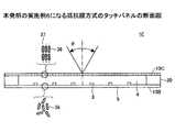
図1及び図2は本発明の実施例1になる抵抗膜方式のタッチパネル1を示す。タッチパネル1は、下側面状部材であるガラス基板2上に、上側面状部材であるPET(polyethylene terephthalate)フィルム10が枠形状の両面接着テープ20によって接着された構成であり、後述するようにカーボンナノチューブを導電体として利用している構造である。X,Yが面方向であり、Zが厚さ方向である。3はスペーサ、4は空間、5、11は透明導電膜、12はハードコート層である。 1 and 2 show a resistive film
ガラス基板2の上面の透明導電膜5及びPETフィルム10の下面の透明導電膜11は、共に、カーボンナノチューブを10%未満分散含有する紫外線硬化型のアクリル樹脂の膜である。 The transparent
ガラス基板2の上面の透明導電膜5は、図3(A)に示すように、透明性の液状の紫外線硬化型のアクリル樹脂にマット材(酸化シリコン)と共にカーボンナノチューブを10%未満練り込んだカーボンナノチューブ混合アクリル樹脂30を用意し、図3(B)、(C)に示すように、ロール31を使用してカーボンナノチューブ混合アクリル樹脂30をガラス基板2の上面に塗布して、塗布膜32を形成し、最後に図3(D)に示すように紫外線35を照射し、アクリル樹脂を硬化させて形成される。透明導電膜5内では、カーボンナノチューブ36は不規則に並んでいる。 As shown in FIG. 3A, the transparent
PETフィルム10の下面の透明導電膜11も、上記と同様にして形成される。 The transparent
PETフィルム10の上面のハードコート層12も、上記と同様にして形成される。 The
ここで、カーボンナノチューブの含有率を10%以上とすると光透過率が低下してしまう。そこで、所望の導電性を有し、しかも、光透過率を無用に低下させないために、カーボンナノチューブの含有率を10%未満に制限してある。 Here, if the carbon nanotube content is 10% or more, the light transmittance is lowered. Therefore, the content of carbon nanotubes is limited to less than 10% in order to have desired conductivity and not to unnecessarily reduce the light transmittance.
タッチ操作した場合に、タッチ操作した個所の透明導電膜11が透明導電膜5と接触して、タッチ操作した個所の座標情報が出力される。 When the touch operation is performed, the transparent
上記構成にタッチパネル1は以下の特性を有する。
(1)光透過率が高い。The
(1) High light transmittance.
カーボンナノチューブを10%未満分散含有するアクリル樹脂の膜は、ITO膜、AG−HC層に比べて、光透過率が高い。よって、タッチパネル1は従来のタッチパネルに比較して光透過率が高い。
(2)ペン入力操作がしやすい。The acrylic resin film containing less than 10% carbon nanotubes has a higher light transmittance than the ITO film and the AG-HC layer. Therefore, the
(2) Pen input operation is easy.
カーボンナノチューブを10%未満分散含有するアクリル樹脂の膜よりなるハードコート層12は、表面の摩擦係数が、AG−HC層に比較して低い。よって、ペンのすべりが良く、ペンを使用した入力操作がしやすい。
(3)指紋がつき難い。The
(3) It is difficult to attach a fingerprint.
カーボンナノチューブを10%未満分散含有するアクリル樹脂の膜よりなるハードコート層12は、良好な撥油性を有し、AG−HC層に比較して指紋がつき難い。 The
なお、前記の紫外線硬化型のアクリル樹脂に代えて、通常の熱硬化型のアクリル樹脂を使用してもよい。 Instead of the ultraviolet curable acrylic resin, a normal thermosetting acrylic resin may be used.
また、カーボンナノチューブ混合アクリル樹脂30はスクリーン印刷しても、或いはスピンコートしてもよい。また、カーボンナノチューブよりなる素材を作成し、これをターゲットとして、半導体プロセスの手法でもって透明導電膜5、11を形成してもよい。 The carbon nanotube mixed
図4は本発明の実施例2になる抵抗膜方式のタッチパネル1Aを示す。タッチパネル1Aは、カーボンナノチューブの光学配向性を利用したものであり、図1及び図2のタッチパネル1とは、PETフィルム10上のハードコート層12Aが相違する。カーボンナノチューブ
ハードコート層12Aは、模式的に示すように、各カーボンナノチューブ30がその軸線31がZ方向を向くように整列している構造である。FIG. 4 shows a
このハードコート層12Aは、図5(A)に示すように、下面に透明導電膜11が形成されたPETフィルム10の上面に、液状の紫外線硬化型のアクリル樹脂にカーボンナノチューブを10%未満練り込んだものをロールコートして塗布膜40を形成し、図5(B)に示すように、電磁石45,46によって磁界をかけ、各カーボンナノチューブ30をその軸線31が磁力線であるZ方向を向くように整列させ、その後に、図5(C)に示すように、紫外線35を照射することによって形成される。 As shown in FIG. 5A, the hard coat layer 12A is formed by kneading carbon nanotubes in a liquid UV curable acrylic resin to less than 10% on the upper surface of the
上記のハードコート層12Aは、各カーボンナノチューブ36がその軸線37がZ方向を向くように整列しているため、光学配向性を有し、可視角度θが例えば60度程度である。よって、タッチパネル1Aを銀行のATMにセットすることによって、タッチパネル1A自体で、正面からは表示が見え、斜めからは表示が見え難くできる。 The hard coat layer 12A has an optical orientation because the
図6は本発明の実施例3になる抵抗膜方式のタッチパネル1Bを示す。タッチパネル1Bは、図1及び図2のタッチパネル1とは、PETフィルム10Bが相違し、且つ、透明導電膜11及びハードコート層12を有しないことが相違する。 FIG. 6 shows a resistive touch panel 1B according to a third embodiment of the present invention. The touch panel 1B is different from the
PETフィルム10Bはカーボンナノチューブが10%未満が混入している構成である。PETフィルム10B自体が導電性を有しており、下面に透明導電膜11は形成されていない。 The
タッチ操作した場合に、タッチ操作した個所のPETフィルム10Bの下面が透明導電膜5と接触して、タッチ操作した個所の座標情報が出力される。 When the touch operation is performed, the lower surface of the
図7は本発明の実施例4になる抵抗膜方式のタッチパネル1Cを示す。タッチパネル1Cは、図6のタッチパネル1Bの変形例であり、図6のタッチパネル1BとはPETフィルム10Cが相違する。 FIG. 7 shows a resistive touch panel 1C according to a fourth embodiment of the present invention. The touch panel 1C is a modification of the touch panel 1B in FIG. 6, and a PET film 10C is different from the touch panel 1B in FIG.
PETフィルム10Cはカーボンナノチューブが10%未満が混入しており、各カーボンナノチューブ30がその軸線31がZ方向を向くように整列している構造である。PETフィルム10Cはそれ自体で導電性を有しており、光学配向性を有し、可視角度θが例えば60度程度である。よって、タッチパネル1Cは銀行のATMにセットされて使用される。 The PET film 10C has a structure in which less than 10% of carbon nanotubes are mixed, and the
このPETフィルム10Cは、図8に示すように、フィルム成形金型50の上下に電磁石51,52を設け、カーボンナノチューブを10%未満練り込んだPETフィルム素材を成形金型50に注入したときに、電磁石51,52を駆動させて、成形途中のPETフィルムに磁界をかけ、各カーボンナノチューブ36をその軸線37がZ方向を向くように整列させることによって製造される。 As shown in FIG. 8, when the PET film 10C is provided with
図9は本発明の実施例5になる抵抗膜方式のタッチパネル1Dを示す。タッチパネル1Dは、下側に下側面状部材であるところの図6に示すPETフィルム10B、上側に上側面状部材であるところの同じく図6に示すPETフィルム10Bを設けた構成である。タッチパネル1Dは湾曲させることが出来、よって彎曲面に沿うようにセット可能である。 FIG. 9 shows a
図10は本発明の実施例6になる抵抗膜方式のタッチパネル1Eを示す。タッチパネル1Eは、下側に図6に示すPETフィルム10B、上側に図7に示すPETフィルム10Cを設けた構成である。タッチパネル1Eは、可視角度θが例えば60度程度であり、且つ、湾曲させることが出来、よって彎曲面に沿うようにセット可能である。 FIG. 10 shows a
図11は本発明の実施例7になる抵抗膜方式のタッチパネル1Fを示す。タッチパネル1Fは、下側に図7に示すPETフィルム10C、上側にも図7に示すPETフィルム10Cを設けた構成である。タッチパネル1Fは、上下のPETフィルム10Cが共に光学配向性を有しているため、可視角度θが例えば30度程度と狭く、且つ、湾曲させることが出来、よって彎曲面に沿うようにセット可能である。 FIG. 11 shows a
1、1A〜1F タッチパネル
2 ガラス基板
3 スペーサ
4 空間
5 透明導電膜
10、10B、10C PETフィルム
11 透明導電膜
12、12A ハードコート層
20 両面接着テープ
30 カーボンナノチューブ混合アクリル樹脂
36 カーボンナノチューブ
37 軸線
45,46、51,52 電磁石
DESCRIPTION OF
Claims (12)
Translated fromJapanese該下側透明導電膜及び該上側透明導電膜は、カーボンナノチューブを分散含有する合成樹脂製の膜よりなる構成としたことを特徴とするタッチパネル。A lower side surface member having a lower transparent conductive film on an upper surface and an upper side surface member having an upper transparent conductive film on a lower surface are disposed with a space interposed therebetween, and the lower transparent conductive film and the upper transparent conductive film are In the touch panel with the opposite configuration,
The touch panel characterized in that the lower transparent conductive film and the upper transparent conductive film are made of a synthetic resin film containing carbon nanotubes in a dispersed manner.
該上側面状部材の上面に、カーボンナノチューブを分散含有する合成樹脂製の膜を有する構成としたことを特徴とするタッチパネル。In the touch panel having a configuration in which the lower side surface member and the upper side surface member are disposed with a space interposed therebetween,
A touch panel comprising a synthetic resin film containing carbon nanotubes dispersed on the upper surface of the upper side surface member.
上記合成樹脂製の膜は、上記カーボンナノチューブが、その軸線が前記上側面状部材の上面に対して垂直となる向きで並んだ構造である構成としたことを特徴とするタッチパネル。The touch panel according to claim 2,
The touch panel characterized in that the synthetic resin film has a structure in which the carbon nanotubes are arranged in a direction in which an axis thereof is perpendicular to an upper surface of the upper side surface member.
前記フィルム状の上側面状部材は、前記カーボンナノチューブがその軸線が前記上側面状部材の面に対して垂直となる向きで並んだ構造である構成としたことを特徴とするタッチパネル。The touch panel according to claim 4,
The touch panel according to claim 1, wherein the film-shaped upper side surface member has a structure in which the carbon nanotubes are arranged in a direction in which an axis thereof is perpendicular to a surface of the upper side surface member.
前記フィルム状の上側面状部材は、前記カーボンナノチューブがその軸線が前記上側面状部材の面に対して垂直となる向きで並んだ構造である構成としたことを特徴とするタッチパネル。The touch panel according to claim 6.
The touch panel according to claim 1, wherein the film-shaped upper side surface member has a structure in which the carbon nanotubes are arranged in a direction in which an axis thereof is perpendicular to a surface of the upper side surface member.
前記フィルム状の上側面状部材は、前記カーボンナノチューブがその軸線が前記上側面状部材の面に対して垂直となる向きで並んだ構造であり、
前記フィルム状の下側面状部材は、前記カーボンナノチューブがその軸線が前記下側面状部材の面に対して垂直となる向きで並んだ構造である構成としたことを特徴とするタッチパネル。The touch panel according to claim 6.
The film-like upper side surface member has a structure in which the carbon nanotubes are arranged in an orientation in which the axis is perpendicular to the surface of the upper side surface member,
The touch panel according to claim 1, wherein the film-like lower side surface member has a structure in which the carbon nanotubes are arranged in a direction in which an axis thereof is perpendicular to a surface of the lower side surface member.
A planar member for a touch panel, comprising carbon nanotubes dispersed therein and arranged such that the carbon nanotubes are aligned in an orientation in which the axis is perpendicular to the plane of the planar member.
Priority Applications (1)
| Application Number | Priority Date | Filing Date | Title |
|---|---|---|---|
| JP2005195571AJP2007011997A (en) | 2005-07-04 | 2005-07-04 | Touch panel |
Applications Claiming Priority (1)
| Application Number | Priority Date | Filing Date | Title |
|---|---|---|---|
| JP2005195571AJP2007011997A (en) | 2005-07-04 | 2005-07-04 | Touch panel |
Publications (1)
| Publication Number | Publication Date |
|---|---|
| JP2007011997Atrue JP2007011997A (en) | 2007-01-18 |
Family
ID=37750345
Family Applications (1)
| Application Number | Title | Priority Date | Filing Date |
|---|---|---|---|
| JP2005195571APendingJP2007011997A (en) | 2005-07-04 | 2005-07-04 | Touch panel |
Country Status (1)
| Country | Link |
|---|---|
| JP (1) | JP2007011997A (en) |
Cited By (41)
| Publication number | Priority date | Publication date | Assignee | Title |
|---|---|---|---|---|
| JP2009104576A (en)* | 2007-10-23 | 2009-05-14 | Kofukin Seimitsu Kogyo (Shenzhen) Yugenkoshi | Touch panel |
| JP2009104577A (en)* | 2007-10-23 | 2009-05-14 | Kofukin Seimitsu Kogyo (Shenzhen) Yugenkoshi | Touch panel |
| EP2073109A2 (en) | 2007-12-21 | 2009-06-24 | Tsing Hua University | Touch panel and display device using the same |
| JP2009146411A (en)* | 2007-12-12 | 2009-07-02 | Qinghua Univ | Touch panel and display using the same |
| JP2009146415A (en)* | 2007-12-12 | 2009-07-02 | Qinghua Univ | Touch panel and display using the same |
| JP2009146416A (en)* | 2007-12-12 | 2009-07-02 | Qinghua Univ | Touch panel and manufacturing method thereof, display using touch panel |
| JP2009146424A (en)* | 2007-12-14 | 2009-07-02 | Qinghua Univ | Touch panel and manufacturing method thereof, display using touch panel |
| JP2009146410A (en)* | 2007-12-12 | 2009-07-02 | Qinghua Univ | Touch panel and display using the same |
| JP2009146417A (en)* | 2007-12-12 | 2009-07-02 | Qinghua Univ | Touch panel and manufacturing method thereof, display using touch panel |
| JP2009146413A (en)* | 2007-12-12 | 2009-07-02 | Qinghua Univ | Touch panel and display using the same |
| JP2009146420A (en)* | 2007-12-14 | 2009-07-02 | Qinghua Univ | Touch panel and display using the same |
| JP2009146423A (en)* | 2007-12-14 | 2009-07-02 | Qinghua Univ | Touch panel and display using the same |
| JP2009146418A (en)* | 2007-12-14 | 2009-07-02 | Qinghua Univ | Touch panel and display using the same |
| JP2009146898A (en)* | 2007-12-12 | 2009-07-02 | Qinghua Univ | Electronic element |
| JP2009146421A (en)* | 2007-12-14 | 2009-07-02 | Qinghua Univ | Touch panel and manufacturing method thereof, display using touch panel |
| JP2009146422A (en)* | 2007-12-14 | 2009-07-02 | Qinghua Univ | Touch panel and display using the same |
| JP2009146414A (en)* | 2007-12-12 | 2009-07-02 | Qinghua Univ | Touch panel and display using the same |
| JP2009151780A (en)* | 2007-12-21 | 2009-07-09 | Qinghua Univ | Touch panel and display using the same |
| JP2009157924A (en)* | 2007-12-27 | 2009-07-16 | Qinghua Univ | Touch control device |
| JP2009163729A (en)* | 2007-12-14 | 2009-07-23 | Qinghua Univ | Touch panel and manufacturing method thereof, display using touch panel |
| US7642463B2 (en) | 2008-01-28 | 2010-01-05 | Honeywell International Inc. | Transparent conductors and methods for fabricating transparent conductors |
| JP2010015576A (en)* | 2008-07-04 | 2010-01-21 | Qinghua Univ | Touch panel |
| JP2010015154A (en)* | 2008-07-04 | 2010-01-21 | Qinghua Univ | Method for manufacturing liquid crystal display panel using touch panel |
| JP2010015153A (en)* | 2008-07-04 | 2010-01-21 | Qinghua Univ | Liquid crystal display panel using touch panel |
| JP2010015577A (en)* | 2008-07-04 | 2010-01-21 | Qinghua Univ | Method for manufacturing for touch panel |
| JP2010015575A (en)* | 2008-07-04 | 2010-01-21 | Qinghua Univ | Liquid crystal display panel using touch panel |
| JP2010020313A (en)* | 2008-07-09 | 2010-01-28 | Qinghua Univ | Manufacturing method of liquid crystal display panel using touch panel |
| JP2010020768A (en)* | 2008-07-09 | 2010-01-28 | Qinghua Univ | Touch panel and display device |
| JP2010020312A (en)* | 2008-07-09 | 2010-01-28 | Qinghua Univ | Liquid crystal display screen using touch panel |
| JP2010049691A (en)* | 2008-08-22 | 2010-03-04 | Qinghua Univ | Personal digital assistant |
| JP2010049692A (en)* | 2008-08-22 | 2010-03-04 | Qinghua Univ | Cellular phone |
| JP2010073208A (en)* | 2008-09-19 | 2010-04-02 | Qinghua Univ | Desk top computer |
| US7727578B2 (en) | 2007-12-27 | 2010-06-01 | Honeywell International Inc. | Transparent conductors and methods for fabricating transparent conductors |
| JP2010153210A (en)* | 2008-12-25 | 2010-07-08 | Nissha Printing Co Ltd | Conductive nanofiber sheet and its manufacturing method |
| JP2010165460A (en)* | 2009-01-13 | 2010-07-29 | Nissha Printing Co Ltd | Conductive nanofiber sheet and method of manufacturing the same |
| US7960027B2 (en) | 2008-01-28 | 2011-06-14 | Honeywell International Inc. | Transparent conductors and methods for fabricating transparent conductors |
| TWI412819B (en)* | 2009-10-09 | 2013-10-21 | Innolux Corp | Capacitive touch panel |
| JP2015038727A (en)* | 2010-03-04 | 2015-02-26 | ガーディアン・インダストリーズ・コーポレーション | Electronic device including transparent conductive coating containing carbon nanotube and nanowire, and method for manufacturing the device |
| US9077793B2 (en) | 2009-06-12 | 2015-07-07 | Tsinghua University | Carbon nanotube based flexible mobile phone |
| US9239651B2 (en) | 2009-10-23 | 2016-01-19 | Samsung Display Co., Ltd. | Touch substrate, method of manufacturing the same and display device having the same |
| WO2021012498A1 (en)* | 2019-07-19 | 2021-01-28 | 苏州维业达触控科技有限公司 | Touch display screen and manufacturing method therefor |
Citations (5)
| Publication number | Priority date | Publication date | Assignee | Title |
|---|---|---|---|---|
| JP2002365427A (en)* | 2001-06-04 | 2002-12-18 | Toray Ind Inc | Polarizer and method for manufacturing the same |
| JP2003215307A (en)* | 2002-01-25 | 2003-07-30 | Nitto Denko Corp | Antireflection film, optical element and image display device |
| JP2004202948A (en)* | 2002-12-26 | 2004-07-22 | Research Laboratory Of Plastics Technology Co Ltd | Laminate |
| JP2005097111A (en)* | 1998-09-21 | 2005-04-14 | Lucent Technol Inc | Process for forming carbon nanotube film device |
| JP2007504504A (en)* | 2003-09-05 | 2007-03-01 | コニンクリユケ フィリップス エレクトロニクス エヌ.ブイ. | Programmable optical components that spatially control the intensity of the radiation beam |
- 2005
- 2005-07-04JPJP2005195571Apatent/JP2007011997A/enactivePending
Patent Citations (5)
| Publication number | Priority date | Publication date | Assignee | Title |
|---|---|---|---|---|
| JP2005097111A (en)* | 1998-09-21 | 2005-04-14 | Lucent Technol Inc | Process for forming carbon nanotube film device |
| JP2002365427A (en)* | 2001-06-04 | 2002-12-18 | Toray Ind Inc | Polarizer and method for manufacturing the same |
| JP2003215307A (en)* | 2002-01-25 | 2003-07-30 | Nitto Denko Corp | Antireflection film, optical element and image display device |
| JP2004202948A (en)* | 2002-12-26 | 2004-07-22 | Research Laboratory Of Plastics Technology Co Ltd | Laminate |
| JP2007504504A (en)* | 2003-09-05 | 2007-03-01 | コニンクリユケ フィリップス エレクトロニクス エヌ.ブイ. | Programmable optical components that spatially control the intensity of the radiation beam |
Cited By (46)
| Publication number | Priority date | Publication date | Assignee | Title |
|---|---|---|---|---|
| JP2009104577A (en)* | 2007-10-23 | 2009-05-14 | Kofukin Seimitsu Kogyo (Shenzhen) Yugenkoshi | Touch panel |
| JP2009104576A (en)* | 2007-10-23 | 2009-05-14 | Kofukin Seimitsu Kogyo (Shenzhen) Yugenkoshi | Touch panel |
| JP2009146898A (en)* | 2007-12-12 | 2009-07-02 | Qinghua Univ | Electronic element |
| JP2010257494A (en)* | 2007-12-12 | 2010-11-11 | Beijing Funate Innovation Technology Co Ltd | Touch panel and display using the same |
| JP2009146411A (en)* | 2007-12-12 | 2009-07-02 | Qinghua Univ | Touch panel and display using the same |
| JP2009146415A (en)* | 2007-12-12 | 2009-07-02 | Qinghua Univ | Touch panel and display using the same |
| JP2009146416A (en)* | 2007-12-12 | 2009-07-02 | Qinghua Univ | Touch panel and manufacturing method thereof, display using touch panel |
| JP2009146410A (en)* | 2007-12-12 | 2009-07-02 | Qinghua Univ | Touch panel and display using the same |
| JP2009146417A (en)* | 2007-12-12 | 2009-07-02 | Qinghua Univ | Touch panel and manufacturing method thereof, display using touch panel |
| JP2009146413A (en)* | 2007-12-12 | 2009-07-02 | Qinghua Univ | Touch panel and display using the same |
| US9040159B2 (en) | 2007-12-12 | 2015-05-26 | Tsinghua University | Electronic element having carbon nanotubes |
| JP2009146414A (en)* | 2007-12-12 | 2009-07-02 | Qinghua Univ | Touch panel and display using the same |
| JP2009146418A (en)* | 2007-12-14 | 2009-07-02 | Qinghua Univ | Touch panel and display using the same |
| JP2009163729A (en)* | 2007-12-14 | 2009-07-23 | Qinghua Univ | Touch panel and manufacturing method thereof, display using touch panel |
| JP2009146421A (en)* | 2007-12-14 | 2009-07-02 | Qinghua Univ | Touch panel and manufacturing method thereof, display using touch panel |
| JP2009146422A (en)* | 2007-12-14 | 2009-07-02 | Qinghua Univ | Touch panel and display using the same |
| JP2009146423A (en)* | 2007-12-14 | 2009-07-02 | Qinghua Univ | Touch panel and display using the same |
| JP2009146424A (en)* | 2007-12-14 | 2009-07-02 | Qinghua Univ | Touch panel and manufacturing method thereof, display using touch panel |
| JP2009146420A (en)* | 2007-12-14 | 2009-07-02 | Qinghua Univ | Touch panel and display using the same |
| JP2009151780A (en)* | 2007-12-21 | 2009-07-09 | Qinghua Univ | Touch panel and display using the same |
| EP2073109A3 (en)* | 2007-12-21 | 2012-08-22 | Tsing Hua University | Touch panel and display device using the same |
| EP2073109A2 (en) | 2007-12-21 | 2009-06-24 | Tsing Hua University | Touch panel and display device using the same |
| US7727578B2 (en) | 2007-12-27 | 2010-06-01 | Honeywell International Inc. | Transparent conductors and methods for fabricating transparent conductors |
| JP2009157924A (en)* | 2007-12-27 | 2009-07-16 | Qinghua Univ | Touch control device |
| US7642463B2 (en) | 2008-01-28 | 2010-01-05 | Honeywell International Inc. | Transparent conductors and methods for fabricating transparent conductors |
| US7960027B2 (en) | 2008-01-28 | 2011-06-14 | Honeywell International Inc. | Transparent conductors and methods for fabricating transparent conductors |
| JP2010015154A (en)* | 2008-07-04 | 2010-01-21 | Qinghua Univ | Method for manufacturing liquid crystal display panel using touch panel |
| JP2010015577A (en)* | 2008-07-04 | 2010-01-21 | Qinghua Univ | Method for manufacturing for touch panel |
| JP2010015576A (en)* | 2008-07-04 | 2010-01-21 | Qinghua Univ | Touch panel |
| JP2010015153A (en)* | 2008-07-04 | 2010-01-21 | Qinghua Univ | Liquid crystal display panel using touch panel |
| JP2010015575A (en)* | 2008-07-04 | 2010-01-21 | Qinghua Univ | Liquid crystal display panel using touch panel |
| JP2010020312A (en)* | 2008-07-09 | 2010-01-28 | Qinghua Univ | Liquid crystal display screen using touch panel |
| JP2010020768A (en)* | 2008-07-09 | 2010-01-28 | Qinghua Univ | Touch panel and display device |
| JP2010020313A (en)* | 2008-07-09 | 2010-01-28 | Qinghua Univ | Manufacturing method of liquid crystal display panel using touch panel |
| JP2011028785A (en)* | 2008-07-09 | 2011-02-10 | Qinghua Univ | Touch panel and display device |
| JP2010049691A (en)* | 2008-08-22 | 2010-03-04 | Qinghua Univ | Personal digital assistant |
| JP2010049692A (en)* | 2008-08-22 | 2010-03-04 | Qinghua Univ | Cellular phone |
| JP2010073208A (en)* | 2008-09-19 | 2010-04-02 | Qinghua Univ | Desk top computer |
| JP2010153210A (en)* | 2008-12-25 | 2010-07-08 | Nissha Printing Co Ltd | Conductive nanofiber sheet and its manufacturing method |
| JP2010165460A (en)* | 2009-01-13 | 2010-07-29 | Nissha Printing Co Ltd | Conductive nanofiber sheet and method of manufacturing the same |
| US9077793B2 (en) | 2009-06-12 | 2015-07-07 | Tsinghua University | Carbon nanotube based flexible mobile phone |
| TWI412819B (en)* | 2009-10-09 | 2013-10-21 | Innolux Corp | Capacitive touch panel |
| US9239651B2 (en) | 2009-10-23 | 2016-01-19 | Samsung Display Co., Ltd. | Touch substrate, method of manufacturing the same and display device having the same |
| US9830038B2 (en) | 2009-10-23 | 2017-11-28 | Samsung Display Co., Ltd. | Touch substrate, method of manufacturing the same and display device having the same |
| JP2015038727A (en)* | 2010-03-04 | 2015-02-26 | ガーディアン・インダストリーズ・コーポレーション | Electronic device including transparent conductive coating containing carbon nanotube and nanowire, and method for manufacturing the device |
| WO2021012498A1 (en)* | 2019-07-19 | 2021-01-28 | 苏州维业达触控科技有限公司 | Touch display screen and manufacturing method therefor |
Similar Documents
| Publication | Publication Date | Title |
|---|---|---|
| JP2007011997A (en) | Touch panel | |
| US10452219B2 (en) | Touch sensor | |
| TWM306694U (en) | Durable resistive touch screen | |
| US9116584B2 (en) | Dielectric layer for touch sensor stack | |
| US20140295150A1 (en) | Method and apparatus for joining together multiple functional layers of a flexible display | |
| TW200912720A (en) | Interactive display system | |
| JP2016018209A (en) | Projector screen and manufacturing method therefor | |
| US20210109615A1 (en) | Resistive pressure sensor device system | |
| US20110064943A1 (en) | Conductive slice structure | |
| CN203085197U (en) | Transparent conductive thin film | |
| CN108710222A (en) | A kind of peep-proof structure and preparation method thereof, display panel assembly | |
| KR20110004778A (en) | Touch panel | |
| KR101956086B1 (en) | Touch panel, display and method of the same | |
| JP2010020769A (en) | Liquid crystal display device using touch panel | |
| JP2011018326A (en) | Conductive plate and touch panel using the same | |
| US9098152B2 (en) | Dielectric layer for touch sensor stack | |
| KR101114646B1 (en) | Touch screen | |
| JP2014002520A (en) | Touch panel and film body | |
| WO2017087210A1 (en) | Touch screen panel with surface having rough feel | |
| US20130269991A1 (en) | Touch panel | |
| CN111386479B (en) | Detachable display device containing polarizing film | |
| CN207937978U (en) | A kind of flexibility touch panel and electronic equipment | |
| CN102915145B (en) | Touch panel | |
| US9229558B2 (en) | Method of manufacturing touch panel and touch panel | |
| KR20150142214A (en) | Touch panel with improved adhesive property to a curved substrate |
Legal Events
| Date | Code | Title | Description |
|---|---|---|---|
| A621 | Written request for application examination | Free format text:JAPANESE INTERMEDIATE CODE: A621 Effective date:20080410 | |
| A977 | Report on retrieval | Free format text:JAPANESE INTERMEDIATE CODE: A971007 Effective date:20100315 | |
| A131 | Notification of reasons for refusal | Free format text:JAPANESE INTERMEDIATE CODE: A131 Effective date:20100323 | |
| A521 | Written amendment | Free format text:JAPANESE INTERMEDIATE CODE: A523 Effective date:20100511 | |
| A02 | Decision of refusal | Free format text:JAPANESE INTERMEDIATE CODE: A02 Effective date:20100928 |