JP2006518551A - Tailoring of nitrogen profiles in silicon oxynitride using rapid thermal annealing and ammonia under ultra-low pressure - Google Patents
Tailoring of nitrogen profiles in silicon oxynitride using rapid thermal annealing and ammonia under ultra-low pressureDownload PDFInfo
- Publication number
- JP2006518551A JP2006518551AJP2006503373AJP2006503373AJP2006518551AJP 2006518551 AJP2006518551 AJP 2006518551AJP 2006503373 AJP2006503373 AJP 2006503373AJP 2006503373 AJP2006503373 AJP 2006503373AJP 2006518551 AJP2006518551 AJP 2006518551A
- Authority
- JP
- Japan
- Prior art keywords
- dielectric film
- forming
- film
- nitrogen
- silicon oxynitride
- Prior art date
- Legal status (The legal status is an assumption and is not a legal conclusion. Google has not performed a legal analysis and makes no representation as to the accuracy of the status listed.)
- Granted
Links
Images


Classifications
- H—ELECTRICITY
- H01—ELECTRIC ELEMENTS
- H01L—SEMICONDUCTOR DEVICES NOT COVERED BY CLASS H10
- H01L21/00—Processes or apparatus adapted for the manufacture or treatment of semiconductor or solid state devices or of parts thereof
- H01L21/02—Manufacture or treatment of semiconductor devices or of parts thereof
- H01L21/04—Manufacture or treatment of semiconductor devices or of parts thereof the devices having potential barriers, e.g. a PN junction, depletion layer or carrier concentration layer
- H01L21/18—Manufacture or treatment of semiconductor devices or of parts thereof the devices having potential barriers, e.g. a PN junction, depletion layer or carrier concentration layer the devices having semiconductor bodies comprising elements of Group IV of the Periodic Table or AIIIBV compounds with or without impurities, e.g. doping materials
- H01L21/20—Deposition of semiconductor materials on a substrate, e.g. epitaxial growth solid phase epitaxy
- H—ELECTRICITY
- H01—ELECTRIC ELEMENTS
- H01L—SEMICONDUCTOR DEVICES NOT COVERED BY CLASS H10
- H01L21/00—Processes or apparatus adapted for the manufacture or treatment of semiconductor or solid state devices or of parts thereof
- H01L21/02—Manufacture or treatment of semiconductor devices or of parts thereof
- H01L21/02104—Forming layers
- H01L21/02107—Forming insulating materials on a substrate
- H01L21/02296—Forming insulating materials on a substrate characterised by the treatment performed before or after the formation of the layer
- H01L21/02318—Forming insulating materials on a substrate characterised by the treatment performed before or after the formation of the layer post-treatment
- H01L21/02321—Forming insulating materials on a substrate characterised by the treatment performed before or after the formation of the layer post-treatment introduction of substances into an already existing insulating layer
- H01L21/02329—Forming insulating materials on a substrate characterised by the treatment performed before or after the formation of the layer post-treatment introduction of substances into an already existing insulating layer introduction of nitrogen
- H01L21/02332—Forming insulating materials on a substrate characterised by the treatment performed before or after the formation of the layer post-treatment introduction of substances into an already existing insulating layer introduction of nitrogen into an oxide layer, e.g. changing SiO to SiON
- H—ELECTRICITY
- H01—ELECTRIC ELEMENTS
- H01L—SEMICONDUCTOR DEVICES NOT COVERED BY CLASS H10
- H01L21/00—Processes or apparatus adapted for the manufacture or treatment of semiconductor or solid state devices or of parts thereof
- H01L21/02—Manufacture or treatment of semiconductor devices or of parts thereof
- H01L21/02104—Forming layers
- H01L21/02107—Forming insulating materials on a substrate
- H01L21/02296—Forming insulating materials on a substrate characterised by the treatment performed before or after the formation of the layer
- H01L21/02318—Forming insulating materials on a substrate characterised by the treatment performed before or after the formation of the layer post-treatment
- H01L21/02337—Forming insulating materials on a substrate characterised by the treatment performed before or after the formation of the layer post-treatment treatment by exposure to a gas or vapour
- H—ELECTRICITY
- H01—ELECTRIC ELEMENTS
- H01L—SEMICONDUCTOR DEVICES NOT COVERED BY CLASS H10
- H01L21/00—Processes or apparatus adapted for the manufacture or treatment of semiconductor or solid state devices or of parts thereof
- H01L21/02—Manufacture or treatment of semiconductor devices or of parts thereof
- H01L21/04—Manufacture or treatment of semiconductor devices or of parts thereof the devices having potential barriers, e.g. a PN junction, depletion layer or carrier concentration layer
- H01L21/18—Manufacture or treatment of semiconductor devices or of parts thereof the devices having potential barriers, e.g. a PN junction, depletion layer or carrier concentration layer the devices having semiconductor bodies comprising elements of Group IV of the Periodic Table or AIIIBV compounds with or without impurities, e.g. doping materials
- H01L21/28—Manufacture of electrodes on semiconductor bodies using processes or apparatus not provided for in groups H01L21/20 - H01L21/268
- H01L21/28008—Making conductor-insulator-semiconductor electrodes
- H01L21/28017—Making conductor-insulator-semiconductor electrodes the insulator being formed after the semiconductor body, the semiconductor being silicon
- H01L21/28158—Making the insulator
- H01L21/28167—Making the insulator on single crystalline silicon, e.g. using a liquid, i.e. chemical oxidation
- H01L21/28185—Making the insulator on single crystalline silicon, e.g. using a liquid, i.e. chemical oxidation with a treatment, e.g. annealing, after the formation of the gate insulator and before the formation of the definitive gate conductor
- H—ELECTRICITY
- H01—ELECTRIC ELEMENTS
- H01L—SEMICONDUCTOR DEVICES NOT COVERED BY CLASS H10
- H01L21/00—Processes or apparatus adapted for the manufacture or treatment of semiconductor or solid state devices or of parts thereof
- H01L21/02—Manufacture or treatment of semiconductor devices or of parts thereof
- H01L21/04—Manufacture or treatment of semiconductor devices or of parts thereof the devices having potential barriers, e.g. a PN junction, depletion layer or carrier concentration layer
- H01L21/18—Manufacture or treatment of semiconductor devices or of parts thereof the devices having potential barriers, e.g. a PN junction, depletion layer or carrier concentration layer the devices having semiconductor bodies comprising elements of Group IV of the Periodic Table or AIIIBV compounds with or without impurities, e.g. doping materials
- H01L21/30—Treatment of semiconductor bodies using processes or apparatus not provided for in groups H01L21/20 - H01L21/26
- H01L21/31—Treatment of semiconductor bodies using processes or apparatus not provided for in groups H01L21/20 - H01L21/26 to form insulating layers thereon, e.g. for masking or by using photolithographic techniques; After treatment of these layers; Selection of materials for these layers
- H01L21/3105—After-treatment
- H—ELECTRICITY
- H10—SEMICONDUCTOR DEVICES; ELECTRIC SOLID-STATE DEVICES NOT OTHERWISE PROVIDED FOR
- H10D—INORGANIC ELECTRIC SEMICONDUCTOR DEVICES
- H10D1/00—Resistors, capacitors or inductors
- H10D1/01—Manufacture or treatment
- H10D1/045—Manufacture or treatment of capacitors having potential barriers, e.g. varactors
- H10D1/047—Manufacture or treatment of capacitors having potential barriers, e.g. varactors of conductor-insulator-semiconductor capacitors, e.g. trench capacitors
- H—ELECTRICITY
- H10—SEMICONDUCTOR DEVICES; ELECTRIC SOLID-STATE DEVICES NOT OTHERWISE PROVIDED FOR
- H10D—INORGANIC ELECTRIC SEMICONDUCTOR DEVICES
- H10D64/00—Electrodes of devices having potential barriers
- H10D64/60—Electrodes characterised by their materials
- H10D64/66—Electrodes having a conductor capacitively coupled to a semiconductor by an insulator, e.g. MIS electrodes
- H10D64/68—Electrodes having a conductor capacitively coupled to a semiconductor by an insulator, e.g. MIS electrodes characterised by the insulator, e.g. by the gate insulator
- H10D64/693—Electrodes having a conductor capacitively coupled to a semiconductor by an insulator, e.g. MIS electrodes characterised by the insulator, e.g. by the gate insulator the insulator comprising nitrogen, e.g. nitrides, oxynitrides or nitrogen-doped materials
- H—ELECTRICITY
- H01—ELECTRIC ELEMENTS
- H01L—SEMICONDUCTOR DEVICES NOT COVERED BY CLASS H10
- H01L21/00—Processes or apparatus adapted for the manufacture or treatment of semiconductor or solid state devices or of parts thereof
- H01L21/02—Manufacture or treatment of semiconductor devices or of parts thereof
- H01L21/02104—Forming layers
- H01L21/02107—Forming insulating materials on a substrate
- H01L21/02109—Forming insulating materials on a substrate characterised by the type of layer, e.g. type of material, porous/non-porous, pre-cursors, mixtures or laminates
- H01L21/02112—Forming insulating materials on a substrate characterised by the type of layer, e.g. type of material, porous/non-porous, pre-cursors, mixtures or laminates characterised by the material of the layer
- H01L21/02123—Forming insulating materials on a substrate characterised by the type of layer, e.g. type of material, porous/non-porous, pre-cursors, mixtures or laminates characterised by the material of the layer the material containing silicon
- H01L21/02126—Forming insulating materials on a substrate characterised by the type of layer, e.g. type of material, porous/non-porous, pre-cursors, mixtures or laminates characterised by the material of the layer the material containing silicon the material containing Si, O, and at least one of H, N, C, F, or other non-metal elements, e.g. SiOC, SiOC:H or SiONC
- H01L21/0214—Forming insulating materials on a substrate characterised by the type of layer, e.g. type of material, porous/non-porous, pre-cursors, mixtures or laminates characterised by the material of the layer the material containing silicon the material containing Si, O, and at least one of H, N, C, F, or other non-metal elements, e.g. SiOC, SiOC:H or SiONC the material being a silicon oxynitride, e.g. SiON or SiON:H
- H—ELECTRICITY
- H01—ELECTRIC ELEMENTS
- H01L—SEMICONDUCTOR DEVICES NOT COVERED BY CLASS H10
- H01L21/00—Processes or apparatus adapted for the manufacture or treatment of semiconductor or solid state devices or of parts thereof
- H01L21/02—Manufacture or treatment of semiconductor devices or of parts thereof
- H01L21/02104—Forming layers
- H01L21/02107—Forming insulating materials on a substrate
- H01L21/02225—Forming insulating materials on a substrate characterised by the process for the formation of the insulating layer
- H01L21/02227—Forming insulating materials on a substrate characterised by the process for the formation of the insulating layer formation by a process other than a deposition process
- H01L21/0223—Forming insulating materials on a substrate characterised by the process for the formation of the insulating layer formation by a process other than a deposition process formation by oxidation, e.g. oxidation of the substrate
- H01L21/02233—Forming insulating materials on a substrate characterised by the process for the formation of the insulating layer formation by a process other than a deposition process formation by oxidation, e.g. oxidation of the substrate of the semiconductor substrate or a semiconductor layer
- H01L21/02236—Forming insulating materials on a substrate characterised by the process for the formation of the insulating layer formation by a process other than a deposition process formation by oxidation, e.g. oxidation of the substrate of the semiconductor substrate or a semiconductor layer group IV semiconductor
- H01L21/02238—Forming insulating materials on a substrate characterised by the process for the formation of the insulating layer formation by a process other than a deposition process formation by oxidation, e.g. oxidation of the substrate of the semiconductor substrate or a semiconductor layer group IV semiconductor silicon in uncombined form, i.e. pure silicon
- H—ELECTRICITY
- H01—ELECTRIC ELEMENTS
- H01L—SEMICONDUCTOR DEVICES NOT COVERED BY CLASS H10
- H01L21/00—Processes or apparatus adapted for the manufacture or treatment of semiconductor or solid state devices or of parts thereof
- H01L21/02—Manufacture or treatment of semiconductor devices or of parts thereof
- H01L21/02104—Forming layers
- H01L21/02107—Forming insulating materials on a substrate
- H01L21/02225—Forming insulating materials on a substrate characterised by the process for the formation of the insulating layer
- H01L21/02227—Forming insulating materials on a substrate characterised by the process for the formation of the insulating layer formation by a process other than a deposition process
- H01L21/02255—Forming insulating materials on a substrate characterised by the process for the formation of the insulating layer formation by a process other than a deposition process formation by thermal treatment
Landscapes
- Engineering & Computer Science (AREA)
- Microelectronics & Electronic Packaging (AREA)
- Condensed Matter Physics & Semiconductors (AREA)
- General Physics & Mathematics (AREA)
- Manufacturing & Machinery (AREA)
- Computer Hardware Design (AREA)
- Physics & Mathematics (AREA)
- Power Engineering (AREA)
- Chemical & Material Sciences (AREA)
- Chemical Kinetics & Catalysis (AREA)
- Crystallography & Structural Chemistry (AREA)
- General Chemical & Material Sciences (AREA)
- Formation Of Insulating Films (AREA)
- Insulated Gate Type Field-Effect Transistor (AREA)
Abstract
Translated fromJapaneseDescription
Translated fromJapanese[0001]本出願は、2003年2月4日出願の米国仮特許第60/445,281号に関し、その利益を主張し、その開示内容は本明細書に全体で援用されている。 [0001] This application claims its benefit with respect to US Provisional Patent No. 60 / 445,281, filed Feb. 4, 2003, the disclosure of which is incorporated herein in its entirety.
1).分野
[0002]本発明は、一般的には、半導体製造の分野に関する。更に詳細には、本発明は、オキシ窒化ケイ素(SiON又はSiOxNy)ゲート誘電体を形成するとともに急速加熱プロセス(RTP)を用いてゲートスタックにそれを集積化する方法に関する。
2).関連技術の説明
[0003]集積回路は、トランジスタ、キャパシタ、抵抗のような、文字通り何百万といった能動デバイスや受動デバイスから作られる。トランジスタ100は、一般的には、ソース102、ドレイン104、ゲートスタック106を含んでいる。ゲートスタック(図1)は、誘電体110(典型的には、二酸化シリコン(SiO2)で製造)を成長させた最上部上の基板108(例えば、典型的にはシリコンで製造)からなり、これは電極112(多結晶シリコンのような導電材料で製造)で覆われている。1).Field
[0002] The present invention relates generally to the field of semiconductor manufacturing. More particularly, the present invention relates to a method of forming a silicon oxynitride (SiON or SiOx Ny ) gate dielectric and integrating it in a gate stack using a rapid heating process (RTP).
2). Explanation of related technology
[0003] Integrated circuits are made up of literally millions of active and passive devices, such as transistors, capacitors, and resistors.
[0004]更にコンピュータ電力を供給するために、デバイスの形を縮小させることによってトランジスタの大きさを小さくする傾向がある。ムーアの法則によるスケーリングには、トランジスタの速度を増加させるために、ゲート駆動電流が増加しなければならないことが必要である。ゲートキャパシタンス(Cox)を増加させることによって、式(1)で示されるゲート駆動電流を増加させることができ、(式(2)で示されるように)誘電体の厚さ(d)を減少させるか又は既存のSiO2誘電体(k=3.9)より誘電率(k)が高い誘電体を用いることによって増加させることができる。[0004] To further supply computer power, there is a tendency to reduce the size of the transistor by reducing the shape of the device. Scaling according to Moore's Law requires that the gate drive current must increase in order to increase the speed of the transistor. By increasing the gate capacitance (Cox ), the gate drive current shown in equation (1) can be increased and the dielectric thickness (d) decreased (as shown in equation (2)). Or can be increased by using a dielectric having a higher dielectric constant (k) than the existing SiO2 dielectric (k = 3.9).

(式中、Ipは駆動電流;μはキャリア移動度、Lgはゲート長、Coxはゲートキャパシタンス、Vppは開放電圧;VTHは閾値電圧;kは誘電率、dは誘電体の厚さ、Aはデバイス面積である。)
[0006]複雑な集積化や材料の取扱いの問題を避けるために、デバイス製造業者は誘電体の厚さをできる限り減少させることによってデバイスパラメータを縮小したい。しかしながら、20オングストローム未満にSiO2の厚さを減少させることにより、トンネル電流の増加のためにゲート信頼性が悪くなり、基板へのホウ素の浸透が増加し、非常に薄い酸化物のプロセス制御が悪くなる。理論では、更に高いkゲート誘電体を用いるという代案は非常に魅力的に思われるが、下に横たわっているSi基板やポリシリコンゲート電極との物質適合性はSiO2を供給するものと適合させることができない。更に、SiO2を用いると、ゲート誘電体として希土類酸化物を導入する場合に扱われるに違いない汚染問題を処理する多くの物質が取り除かれる。(Where Ip is the drive current; μ is the carrier mobility, Lg is the gate length, Cox is the gate capacitance, Vpp is the open circuit voltage, VTH is the threshold voltage, k is the dielectric constant, and d is the dielectric thickness. A is the device area.)
[0006] To avoid complex integration and material handling problems, device manufacturers want to reduce device parameters by reducing the dielectric thickness as much as possible. However, reducing the SiO2 thickness to less than 20 Angstroms degrades gate reliability due to increased tunneling current, increases boron penetration into the substrate, and allows very thin oxide process control. Deteriorate. In theory, the alternative of using a higher k-gate dielectric seems very attractive, but the material compatibility with the underlying Si substrate or polysilicon gate electrode is compatible with that supplying SiO2 . I can't. Furthermore, the use of SiO2, a number of substances that handles the differences no contamination problems are dealt with when introducing rare-earth oxide as gate dielectric is removed.
[0007]0.1μmテクノロジーノード以降までSiO2を拡張させる際に直面する難題は、(1)P+ホウ素(B)がゲートオキサイドへのゲート電極や下に横たわるSi基板をドープしたPMOSデバイスのようなトランジスタにおけるホウ素浸透を含んでいる。また、(2)ゲートオキサイドの厚さの減少に伴うゲートリーケージ電流の増加を含んでいる。[0007] The challenges faced when extending SiO2 beyond the 0.1 μm technology node are: (1) P + boron (B), such as a PMOS device doped with a gate electrode to the gate oxide or an underlying Si substrate Includes boron permeation in such transistors. In addition, (2) an increase in gate leakage current accompanying a decrease in gate oxide thickness is included.
[0008]オキシ窒化ケイ素(SiOxNy或いはSiON)を形成するSiO2層の窒化物形成は、SiO2誘電体を0.1μmデバイス世代に小さくする有望な候補として発展してきた。誘電体膜に窒素を注入すると、ホウ素が遮断されるとともにゲート誘電体の誘電率が増加する。誘電率の増加は、より厚い誘電体が純粋なSiO2に対して用いることができることを意味し、それ故、ゲートリーケージ電流が減少する。超薄(例えば、12オングストローム)ゲート誘電体として上記難題を克服するのに効果的である窒素(N)ドーピングの場合、ゲート誘電体の上面で窒素濃度プロファイルのピークを有する誘電体膜中の高い(≧5%)全窒素濃度を有することが不可欠である。[0008] The nitridation of the SiO2 layer forming silicon oxynitride (SiOx Ny or SiON) has evolved as a promising candidate for reducing the SiO2 dielectric to the 0.1 μm device generation. When nitrogen is implanted into the dielectric film, boron is blocked and the dielectric constant of the gate dielectric increases. An increase in dielectric constant means that a thicker dielectric can be used for pure SiO2 , thus reducing the gate leakage current. In the case of nitrogen (N) doping, which is effective in overcoming the above challenges as an ultra-thin (e.g., 12 angstrom) gate dielectric, high in the dielectric film having a nitrogen concentration profile peak on the top surface of the gate dielectric. It is essential to have a total nitrogen concentration (≧ 5%).
[0009]伝統的に、熱プロセスは1回に複数のウエハ(5-100枚)を処理する炉で行われてきた。炉は大容積であり、この莫大な容積を排気することは困難である。このことは、たいていの熱プロセスの成長速度がプロセス圧力の低下とともに減速するという事実によって、大気圧(760Torr)又はわずかに大気圧(>500Torr)未満で通常行われている熱プロセスがもたらされたことと結びついた。 [0009] Traditionally, thermal processes have been performed in furnaces that process multiple wafers (5-100) at a time. The furnace has a large volume, and it is difficult to exhaust this huge volume. This is due to the fact that the growth rate of most thermal processes slows down with decreasing process pressure, resulting in thermal processes that are usually performed at atmospheric pressure (760 Torr) or slightly below atmospheric pressure (> 500 Torr). It was tied to that.
[0010]熱的に成長したオキシ窒化ケイ素は、0.2μmから0.13μmへのデバイス世代の数年間ゲート絶縁層として用いられてきた。デバイス技術が0.2μmから0.1μmに進歩するにつれて、ゲートオキサイドは>25オングストロームから<12オングストロームに薄くされてきた。従って、ホウ素を遮断するとともにゲートリーケージ電流を減少させるために、膜中の窒素量は<3%から5-10%に増加されなければならない。一酸化窒素(NO)や亜酸化窒素(N2O)がオキシ窒化物ゲート誘電体を成長させる場合、オキシ窒化物が成長するにつれて、Nが誘電体膜に同時に取込まれる。それ故、窒素が膜に均等に分配される。既存のSiO2層を高温でアニールすることによりオキシ窒化ケイ素を形成するためにNO又はN2Oが用いられる場合には、窒素がSi‐基板/酸化物インタフェースでSiONを成長させることによって取込まれた。従って、窒素がインタフェースに取込まれる。後者の場合(<2%)における窒素量は、前者の場合(4−5%)より少ない。[0010] Thermally grown silicon oxynitride has been used as a gate insulating layer for several years in the device generation from 0.2 μm to 0.13 μm. As device technology has progressed from 0.2 μm to 0.1 μm, gate oxide has been thinned from> 25 angstroms to <12 angstroms. Therefore, the amount of nitrogen in the film must be increased from <3% to 5-10% in order to block boron and reduce the gate leakage current. When nitric oxide (NO) or nitrous oxide (N2 O) grows an oxynitride gate dielectric, N is simultaneously incorporated into the dielectric film as the oxynitride grows. Therefore, nitrogen is evenly distributed across the membrane. If NO or N2 O is used to form silicon oxynitride by annealing an existing SiO2 layer at high temperature, nitrogen is captured by growing SiON at the Si-substrate / oxide interface. Mareta. Therefore, nitrogen is taken into the interface. The amount of nitrogen in the latter case (<2%) is less than in the former case (4-5%).
[0011]N2Oで直接成長したオキシ窒化ケイ素、又はN2Oを含むSiO2膜をアニールすることによって形成されたオキシ窒化ケイ素は、更に高度な(0.2μm)技術世代デバイスの最良の候補であった。膜中<2%の窒素が>25オングストローム厚ゲート誘電体によるデバイス性能を高めるために十分であった。0.13μmにデバイス技術が発展してきたので、ドープされていないSiO2と比べてリーケージ電流を減少させ且つホウ素が更に薄い誘電体を通って基板に拡散するのを防止するために、膜中の窒素はNO直接成長又はNOアニールを用いることによって<2%から4‐5%に増加しなければならなかった。これらのどちらか1つの技術により取込まれた窒素量は不十分であり、窒素濃度プロファイルは、SiONを前に説明した0.1μmデバイス世代に拡張するのに不適当である。プロセス圧力を低くすると、膜への窒素取込みの速度が低下するだけであり、従って、窒化物形成プロセスが高圧で実施され続けた。[0011] Direct grown silicon oxynitride with N2 O, or silicon oxynitride formed by annealing the SiO2 film containing N2 O is further advanced (0.2 [mu] m) the best technology generation device It was a candidate. <2% nitrogen in the film was sufficient to enhance device performance with> 25 Angstrom thick gate dielectric. As device technology has evolved to 0.13 μm, in order to reduce the leakage current compared to undoped SiO2 and prevent boron from diffusing through the thinner dielectric into the substrate, Nitrogen had to be increased from <2% to 4-5% by using NO direct growth or NO annealing. The amount of nitrogen incorporated by either one of these techniques is inadequate and the nitrogen concentration profile is unsuitable for extending SiON to the 0.1 μm device generation previously described. Lowering the process pressure only reduced the rate of nitrogen incorporation into the film, and thus the nitridation process continued to be performed at higher pressures.
[0012]最近では、プラズマ窒化物形成がゲートオキサイドを窒化するために(窒素を取込むために)用いられてきた。この技術によって、ポリゲート/酸化物インタフェースに高窒素濃度が生じ、酸化物誘電体へのホウ素浸透が防止される。同時に、酸化物誘電体のバルクは、プラズマ窒化物形成プロセス中に会合されていない窒素で軽くドープされ、開始酸化物上の電気的な酸化物の厚さ(EOT)が減少する。プラズマ窒化物形成プロセスは、特に金属汚染やデバイスに対してプラズマ損傷を引き起こし得るプラズマハードウェアを必要とし、フロントエンド処理に最適化された従来の熱処理ハードウェアに比べて維持することが難しい。プラズマ窒化物形成が現在直面している難題は、デバイスパラメータである電気的な酸化物の厚さ(EOT)の<11オングストロームまでの縮小、移動度の低下、高性能適用の超薄膜誘電体(開始酸化物<10オングストローム)による駆動電流(Idsat)の減少である。 [0012] Recently, plasma nitridation has been used to nitride gate oxide (to incorporate nitrogen). This technique creates a high nitrogen concentration at the polygate / oxide interface and prevents boron penetration into the oxide dielectric. At the same time, the bulk of the oxide dielectric is lightly doped with unassociated nitrogen during the plasma nitridation process, reducing the electrical oxide thickness (EOT) on the starting oxide. The plasma nitridation process requires plasma hardware that can cause plasma damage, particularly to metal contamination and devices, and is difficult to maintain compared to conventional heat treatment hardware optimized for front end processing. The challenges currently faced by plasma nitridation include the reduction of device parameters, electrical oxide thickness (EOT) to <11 angstroms, lower mobility, ultra-thin dielectrics for high performance applications ( Reduced drive current (Idsat) due to starting oxide <10 angstroms.
[0013]最近に採用された他の選択肢は、熱アンモニア(NH3)アニールであり、5%を超える窒素を取込むことが証明され、あるプロセス条件下でインタフェースより誘電体の表面で窒素濃度が高くなり得る。しかしながら、この化学は、種々の理由でNO又はN2O化学反応ほど一般的でなかった。O2又は水蒸気(H2O)の不純物はppmレベルでさえ膜中の窒素取込みを妨げることがあり、一貫性のない結果も与えることがあるので、NH3化学は熱窒化物形成のための炉を用いた場合に生産価値があった。ウエハ装填中の炉処理の場合、大量の空気と水蒸気が炉に入り、かなりの量の時間が除去に取られ、炉のエッジから中心にウエハの膜に一貫しない窒素取込みが生じる。NOやN2O化学と異なり、NH3アニールによって、ホットエレクトロンが生じる誘電体内への水素取込みが生じ、デバイスの信頼性の問題が生じる。オキシ窒化ケイ素膜中の水素が、不活性(N2又はAr)又はO2周囲において短時間高温でポスト窒化形成アニールすることによって排除し得ることが示された。[0013] Another option recently adopted is thermal ammonia (NH3 ) annealing, which has proven to incorporate more than 5% nitrogen and has a nitrogen concentration at the surface of the dielectric rather than the interface under certain process conditions. Can be expensive. However, this chemistry has not been as general as the NO or N2 O chemistry for various reasons. NH3 chemistry is responsible for thermal nitridation because impurities in O2 or water vapor (H2 O) can interfere with nitrogen uptake in the film, even at ppm levels, and can give inconsistent results. There was production value when using a furnace. In the case of a furnace process during wafer loading, a large amount of air and water vapor enters the furnace and a significant amount of time is taken for removal, resulting in inconsistent nitrogen uptake in the wafer film centered from the furnace edge. Unlike NO and N2 O chemistry, NH3 annealing causes the incorporation of hydrogen into the dielectric, where hot electrons are generated, resulting in device reliability issues. It has been shown that hydrogen in a silicon oxynitride film can be eliminated by post-nitridation annealing at high temperatures for a short time around inert (N2 or Ar) or O2 .
[0014]急速加熱処理(RTP)の出現とクラスタタイプツールにおける他の処理チャンバによる集積化とともに、膜がO2又はH2O不純物を含まずに制御された雰囲気において効果的に窒化することができ、膜中の水素がRTPアニールによって取り除くことができるので、NH3プロセスが生産価値のあるものになってきた。しかしながら、インタフェースピークの問題は未だに残ったままである。既存の技術においては、塩基酸化物SiO2膜(単一ウエハRTPチャンバ又は炉で成長させた)は、高温(>850℃)、大気圧(760Torr)又は大気圧未満(>500Torr)で、純粋なNH3又はNH3と不活性ガス(N2又はAr)の混合物のいずれかを含有する雰囲気に供される。しかしながら、これにより開始SiO2膜内に窒素の二頂分布が生じ、第一窒素ピークがオキシ窒化ケイ素面(又は時々ポリシリコンキャップ/オキシ窒化ケイ素インタフェース)に、第二ピークがオキシ窒化ケイ素/基板インタフェースにあることが見出された。このような二頂分布は、100Torr程度の反応圧力でさえ見出された。第一ピークは、ホウ素遮断や誘電率の増加のようなデバイスに良好な電気的性質を与える原因となり、それによって同様の電気的な厚さの開始酸化物に比べてデバイスのリーケージ電流が減少する。もう一方の第二ピークはゲートスタックに不十分なインタフェース特性を与え、結果として閾値電圧移動が大きくなり、トランジスタの電荷キャリアの移動度が低下する。[0014] With the advent of rapid thermal processing (RTP) and integration with other processing chambers in cluster type tools, the film can be effectively nitrided in a controlled atmosphere free of O2 or H2 O impurities. And the hydrogen in the film can be removed by RTP annealing, making the NH3 process valuable. However, the interface peak problem still remains. In existing technology, a base oxide SiO2 film (grown in a single wafer RTP chamber or furnace) is pure at high temperature (> 850 ° C.), atmospheric pressure (760 Torr) or below atmospheric pressure (> 500 Torr). Or an atmosphere containing either NH3 or a mixture of NH3 and an inert gas (N2 or Ar). However, this creates a bimodal distribution of nitrogen in the starting SiO2 film, with the first nitrogen peak at the silicon oxynitride surface (or sometimes the polysilicon cap / silicon oxynitride interface) and the second peak at the silicon oxynitride / substrate It was found to be in the interface. Such a bimodal distribution was found even at a reaction pressure on the order of 100 Torr. The first peak causes the device to give good electrical properties such as boron blockage and increased dielectric constant, thereby reducing the leakage current of the device compared to the starting oxide of similar electrical thickness. . The other second peak imparts insufficient interface characteristics to the gate stack, resulting in increased threshold voltage movement and reduced charge carrier mobility in the transistor.
[0015]NH3によるゲートオキサイドの熱窒化物形成速度論について、80‐100オングストロームのゲートオキサイドを研究した。0.1μmデバイステクノロジーノード以降において有効であるオキシ窒化ケイ素誘電体膜の場合、厚さは低リーケージ電流トランジスタデバイスにおいて<25オングストローム、高性能トランジスタにおいて<12オングストロームでなければならない。オキシ窒化ケイ素形成に現在用いられる高圧NH3プロセスは、オキシ窒化ケイ素/基板インタフェースで高窒素濃度を生じ、結果としてデバイス性能が悪くなり、0.1μmテクノロジー以降このプロセスの縮小を制限している。[0015] For thermal nitridation kinetics of the gate oxide due to NH3, it was studied gate oxide 80-100 Angstroms. For silicon oxynitride dielectric films that are effective after the 0.1 μm device technology node, the thickness should be <25 Å for low leakage current transistor devices and <12 Å for high performance transistors. The high pressure NH3 process currently used for silicon oxynitride formation results in high nitrogen concentrations at the silicon oxynitride / substrate interface, resulting in poor device performance, limiting this process shrinkage since the 0.1 μm technology.
[0016]SiO2のような誘電体膜に窒素を取込む現在の方法は、NH3による超薄膜オキシ窒化シリコン(SiON又はSiOxNy)膜を形成するとともに高性能と低リーケージ電流適用双方の0.1μmデバイスの先進技術ノード以降での使用に縮小するためにゲートスタックへ集積化するのに有効ではない。以下から明らかなように、本発明の実施形態は当該技術において長期の要求や要望を満たしている。[0016] Current methods of incorporating nitrogen into dielectric films such as SiO2 form ultra-thin silicon oxynitride (SiON or SiOx Ny ) films with NH3 and apply both high performance and low leakage currents The 0.1 μm device is not effective for integration into the gate stack in order to reduce its use beyond the advanced technology node. As will be apparent from the following, embodiments of the present invention meet long-term needs and desires in the art.
[0017]本発明の態様によれば、誘電体膜を形成する方法は、窒化物形成ガスと急速加熱アニールプロセスを用いて窒素を誘電体膜に取込むことを含んでいる。約10Torr以下の超低圧は、急速加熱アニールプロセスに用いられる。 [0017] According to an aspect of the present invention, a method of forming a dielectric film includes incorporating nitrogen into the dielectric film using a nitridation gas and a rapid thermal annealing process. Ultra-low pressures of about 10 Torr or less are used for rapid thermal annealing processes.
[0018]本発明の他の態様によれば、ゲートスタックを形成する方法は、基板上に二酸化シリコン膜を形成することを含んでいる。その後、窒素が急速加熱アニールプロセスと窒化ガスを用いて二酸化シリコン膜に取込まれ、ここで、急速加熱アニールプロセスは約10Torrで起こる。窒素が取込まれた後、二酸化シリコン膜はオキシ窒化ケイ素膜となる。急速加熱アニールプロセスは、約5%以上の窒素濃度を有するオキシ窒化ケイ素膜を形成するのに十分な時間二酸化シリコン膜に取込むべき窒素の窒化ガスで続けられる。キャップ層がオキシ窒化ケイ素上に形成される。 [0018] According to another aspect of the invention, a method of forming a gate stack includes forming a silicon dioxide film on a substrate. Nitrogen is then incorporated into the silicon dioxide film using a rapid thermal annealing process and a nitriding gas, where the rapid thermal annealing process occurs at about 10 Torr. After nitrogen is taken in, the silicon dioxide film becomes a silicon oxynitride film. The rapid thermal annealing process is continued with a nitrogen nitriding gas to be incorporated into the silicon dioxide film for a time sufficient to form a silicon oxynitride film having a nitrogen concentration of about 5% or greater. A cap layer is formed on the silicon oxynitride.
[0019]本発明の他の態様によれば、ゲートスタックを形成する方法は、窒化物形成ガスと急速加熱アニールプロセスを用いて二酸化シリコン膜に窒素を取込むことを含んでいる。約10Torr以下の超低圧は、急速加熱アニールに用いられる。誘電体膜に窒素を取込むとオキシ窒化ケイ素膜が形成する。オキシ窒化ケイ素を形成するのに十分な量の窒素が二酸化シリコン膜に取込まれた後、オキシ窒化ケイ素膜はポストアニールされる。 [0019] According to another aspect of the present invention, a method of forming a gate stack includes incorporating nitrogen into a silicon dioxide film using a nitridation gas and a rapid thermal annealing process. An ultra-low pressure of about 10 Torr or less is used for rapid thermal annealing. When nitrogen is taken into the dielectric film, a silicon oxynitride film is formed. After a sufficient amount of nitrogen has been incorporated into the silicon dioxide film to form silicon oxynitride, the silicon oxynitride film is post-annealed.
[0020]本発明の実施形態は例として示され、添付の図面に限定されず、同様の符号は同じ要素を意味する。 [0020] Embodiments of the present invention are shown by way of example and are not limited to the accompanying drawings, in which like numerals refer to the same elements.
[0021]表1は、二酸化シリコン膜に窒素を取込む種々の方法を比較する表である。 [0021] Table 1 compares various methods for incorporating nitrogen into a silicon dioxide film.
[0028]本発明の実施形態は、アンモニアと超低処理圧(例えば、約10Torr以下)による急速加熱アニールプロセスを用いて、SiON又はSiOxNyのような窒素を含む誘電体膜を形成する新規な方法を含んでいる。以下の説明においては、説明のための多くの個々の詳細が本発明の十分な理解を与えるために示されている。しかしながら、本発明がこれらの個々の詳細を含まずに実施することができることは当業者に明らかである。他の例においては、個々の装置構造及び方法は本発明を不明瞭にしないように記載されていない。以下の説明と図面は本発明の例示であり、本発明を制限するものとして解釈すべきでない。[0028] Embodiments of the present invention, ammonia and ultra-low processing pressure (e.g., about 10Torr or less) using a rapid thermal annealing process by, forming a dielectric film containing nitrogen such as SiON or SiOx Ny Includes new methods. In the following description, numerous specific details are set forth in order to provide a thorough understanding of the present invention. However, it will be apparent to one skilled in the art that the present invention may be practiced without these specific details. In other instances, individual device structures and methods have not been described so as not to obscure the present invention. The following description and drawings are illustrative of the invention and are not to be construed as limiting the invention.
[0029]一実施形態においては、本明細書においてRTA−NH3と呼ぶ急速アニールプロセスとNH3の存在とを用いてオキシ窒化ケイ素誘電体膜を形成する方法を提供する。オキシ窒化ケイ素膜を形成するための処理圧は、超低圧(約10Torr以下)である。更に、処理圧力を変化させると、オキシ窒化ケイ素膜における窒素の量と分布のテイラリングが可能になる。[0029] In one embodiment, there is provided a method of forming a silicon oxynitride dielectric film using the presence of a rapid thermal annealing process and NH3 referred to as RTA-NH3 herein. The processing pressure for forming the silicon oxynitride film is an ultra-low pressure (about 10 Torr or less). Furthermore, tailoring the amount and distribution of nitrogen in the silicon oxynitride film is possible by changing the processing pressure.
[0030]他の実施形態においては、RTA−NH3プロセスを用いて形成されたオキシ窒化ケイ素膜(SiON膜又はSiOxNy膜)をトランジスタを形成するためのゲートスタックに集積化する方法を提供する。[0030] In another embodiment, a method of integrating a silicon oxynitride film (SiON film or SiOx Ny film) formed using an RTA-NH3 process into a gate stack for forming a transistor. provide.
[0031]一実施形態においては、二酸化シリコン(SiO2)膜がその上に形成された基板は、急速加熱アニール(RTA)プロセスを実施するように構成された単一ウエハ急速加熱アニール(RTP)チャンバ内でアンモニアガスに供される。基板は、半導体デバイスを製造するために当該技術において典型的に用いられる単結晶シリコンウエハ又はシリコンウエハであり得る。SiO2膜の厚さは、一実施形態において約30オングストローム未満であってもよい。一実施形態においては、RTPチャンバへのアンモニアガスフローは、約100sccm〜5slmの範囲にある。ガスフローが処理チャンバのサイズに依存して変化させることができることは理解されるべきである。例えば、上記ガスフローは、200mm単一ウエハリアクタチャンバ用である。リアクタ容積の増加による300mm単一ウエハリアクタチャンバについて、ガスフローは比例して増加することができる。一実施形態においては、処理温度は900‐1100℃の範囲にあり、処理圧力は約10Torr以下、又は0.010Torr〜約10Torrの範囲にあることができる。プロセスは、純粋なアンモニア又はアルゴン又は窒素のような不活性ガスで希釈されたアンモニアのどちらかを用いる。結果として、SiON又はSiOxNyが形成される。[0031] In one embodiment, a substrate having a silicon dioxide (SiO2 ) film formed thereon is a single wafer rapid thermal anneal (RTP) configured to perform a rapid thermal anneal (RTA) process. It is supplied to ammonia gas in the chamber. The substrate can be a single crystal silicon wafer or a silicon wafer typically used in the art to manufacture semiconductor devices. The thickness of the SiO2 film may be less than about 30 Å in one embodiment. In one embodiment, the ammonia gas flow into the RTP chamber is in the range of about 100 sccm to 5 slm. It should be understood that the gas flow can be varied depending on the size of the processing chamber. For example, the gas flow is for a 200 mm single wafer reactor chamber. For a 300 mm single wafer reactor chamber with increased reactor volume, the gas flow can be increased proportionally. In one embodiment, the processing temperature can be in the range of 900-1100 ° C. and the processing pressure can be about 10 Torr or less, or in the range of 0.010 Torr to about 10 Torr. The process uses either pure ammonia or ammonia diluted with an inert gas such as argon or nitrogen. As a result, SiON or SiOx Ny is formed.
[0032]一実施形態においては、アプライドマテリアルズ社で製造されたXE、XE Plus又はRadianceのような市販で入手できる減圧RTPチャンバハードウェアが、RTA‐NH3プロセスを実施するために用いられてSiON又はSiOxNy膜を形成する。このような減圧RTPチャンバは、RTA‐NH3を用いてSiON又はSiOxNyの形成のために超低処理圧(例えば、1Torr以下)を与える。一実施形態においては、ターボポンプが、RTPチャンバの全圧を約0.010Torr(又は10mTorr)に低下させるのに援助するために、RTPチャンバに接続又は付加することができる。[0032] In one embodiment, XE manufactured by Applied Materials, Inc., under reduced pressure RTP chamber hardware available commercially, such as XE Plus or Radiance is used to implement the RTA-NH3 process A SiON or SiOx Ny film is formed. Such a reduced pressure RTP chamber provides a very low processing pressure (eg, 1 Torr or less) for the formation of SiON or SiOx Ny using RTA-NH3 . In one embodiment, a turbo pump can be connected or added to the RTP chamber to assist in reducing the total pressure in the RTP chamber to about 0.010 Torr (or 10 mTorr).
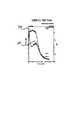
[0033]SiON又はSiOxNy膜がアンモニア存在下に高圧(例えば、100Torr)でRTAによって形成される場合、飛行時間型二次イオン質量分析法(TOF‐SIMS)と呼ばれる方法によって測定されるようにSiON又はSiOxNy膜における窒素濃度プロファイルは、窒素濃度プロファイルが図2に示されるように2つのピーク202と204を有することを示すことが見出される。第一ピーク204は窒素濃度が酸化物表面で高い(約4×10²¹単位)ことを示し、第二ピーク202は、基板インタフェースで十分な量の窒素濃度(約4×10²¹単位)があることを示している。[0033] When a SiON or SiOx Ny film is formed by RTA at high pressure (eg, 100 Torr) in the presence of ammonia, it is measured by a method called time-of-flight secondary ion mass spectrometry (TOF-SIMS) Thus, the nitrogen concentration profile in the SiON or SiOx Ny film is found to indicate that the nitrogen concentration profile has two
[0034]処理圧力、温度及び時間のようなプロセス条件を変えると、2つのピーク204と202の強度の比率を変化させ得ることが本発明者らによって発見された。図3A‐図3Eに示されるように、プロセス圧はピーク202と204の強度の比率に非常に影響する。図3A‐図3Eに示されるように、圧力が1000℃の一定の温度で100Torrから0.250Torrに低下するときに、基板インタフェースの第二ピーク202は完全に消失する。図3Aから分かるように、SiON又はSiOxNy膜が約100Torrの圧力においてRTA‐NH3を用いて形成されるときに、2つのピーク202とび204が存在する。図3Bにおいては、SiON又はSiOxNy膜が約10Torrの圧力においてRTA‐NH3を用いて形成されるときに、ピーク202が低下し、基板インタフェースの窒素濃度が低下することを示している。同様に、図3C‐3Eに示されるように、約0.25Torrのプロセス圧でほとんど排除されるまで、ピーク202が低下する。[0034] It has been discovered by the inventors that varying process conditions such as process pressure, temperature and time can change the ratio of the intensity of the two
[0035]更に、超低圧(例えば、約10Torr以下)でSiON又はSiOxNy膜を形成しつつ温度を増加させると、図4A−4Cに示されるように窒素濃度ピーク204が高められる。例えば、図3Bにおいては、SiON又はSiOxNy膜を形成するために用いた窒化物形成が約10Torr、約1000℃でRTA−NH3を用いて行われた場合、ピーク204は約3.2×10²¹濃度単位である。図4Cにおいては、SiON又はSiOxNy膜がを形成するために用いられる窒化物形成が、約10Torr、約1100℃(100℃高い)でRTA−NH3を用いて行われた場合、ピーク204は約6×10²¹濃度単位である。[0035] Further, increasing the temperature while forming the SiON or SiOx Ny film at ultra-low pressure (eg, about 10 Torr or less) increases the
[0036]従って、超低圧(約≦10Torr)、高温(≧1000−1100℃)でSiON又はSiOxNy膜を形成することが最適である。第一ピーク204で高窒素濃度(SiON又はSiOxNy膜の表面で)で、基板インタフェースで低い又はほぼ最低の窒素濃度を有すると、≦0.1μm先進テクノロジーノードの超薄膜ゲート誘電体の理想的なプロファイルが示される。Therefore, it is optimal to form a SiON or SiOx Ny film at ultra-low pressure (about ≦ 10 Torr) and high temperature (≧ 1000-1100 ° C.). With a high nitrogen concentration at the first peak 204 (at the surface of the SiON or SiOx Ny film) and a low or near minimum nitrogen concentration at the substrate interface, the ultra-thin gate dielectric of the ≦ 0.1 μm advanced technology node An ideal profile is shown.
[0037]低圧で、SiON又はSiOxNy膜における窒素濃度量は、温度を変化させることによって、或いは処理温度を一定に維持しつつプロセス時間を変化させることによっても調整することができる。例えば、同様の品質のSiON又はSiOxNy膜は、約1000℃、10Torrで10秒間、又は約1000℃、1Torrで45秒間のどちらかのRTA−NH3プロセスを用いた6オングストロームの二酸化シリコンを窒化物形成することによって形成される。従って、一定の温度で圧力を低下させると、同等の厚さの膜で同じ窒素量を達成するために時間を増加させる必要がある。[0037] at low pressure, the nitrogen concentration amount of SiON or SiOx Ny film can be adjusted by changing the process time by changing the temperature, or by while maintaining the process temperature constant. For example, similar SiON or SiOx Ny film quality is about 1000 ° C., 10 seconds at 10 Torr, or about 1000 ° C., 6 Å of the silicon dioxide used either RTA-NH3 process for 45 seconds at 1Torr Is formed by forming a nitride. Thus, when the pressure is reduced at a constant temperature, it is necessary to increase the time to achieve the same amount of nitrogen in equivalently thick films.
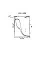
[0038]図5は、プラズマ窒化物形成プロセスとRTA−NH3プロセスを用いて製造されたSiON又はSiOxNy膜の窒素濃度プロファイルを比較する図である。一実施形態においては、用いられたプラズマ窒化物形成プロセスは、当該技術で既知の脱結合プラズマ窒化物形成(DPN)である。DPNは、窒素プラズマを生成するとともに高レベルの窒素を酸化物膜上に取込む誘導結合を用いた技術である。DPNは、酸化物/基板インタフェースで窒素が少なく、酸化物表面で窒素濃度が多いオキシ窒化ケイ素膜の形成を可能にする。DPNにおいては、例えば、SiO2膜の表面に、SiO2膜を分解し且つ窒素イオンをSiO2膜に結合する窒素イオンを衝突させ、SiON又はSiOxNy膜を形成する。従ってSiO2膜は脱結合窒素プラズマに晒される。一実施形態においては、DPNは、流量が約100‐200sccmの範囲にあり、約300ワットのプラズマ電力の窒素ガスの存在下に、圧力が約5‐20mTorr又は10Torr未満の範囲にあるチャンバで行われる。DPNプロセスパラメータは、当該技術において既知であるチャンバサイズと容積に依存して変化させることができる。PDNは、基板インタフェースで第二ピーク202を有しないSiON又はSiOxNy膜を生成する。更に、DPNとRTA‐NH3プロセスの両プロセスにおいては、SiON又はSiOxNy膜は、誘電体膜の上面で窒素(Ny)濃度が最も高く、“y”は深さが減少することによって特徴付けられる。しかしながら、DPNプロセスの窒素濃度プロファイルの尾部は、図5Bを‐5Cに示されるように超低処理圧で行われるRTA−NH3プロセスよりSi基板近くに拡張されるように見える。このことは、プラズマ窒化物形成プロセスを用いて形成されたSiON又はSiOxNy膜よりRTA‐NH3処理を用いて形成されたSiON又はSiOxNy膜を組込んでいるデバイスの高駆動電流に反映される。また、RTA‐NH3処理を用いて形成されたSiON又はSiOxNy膜は、会合されていない窒素がない。DPNプロセスよりRTA‐NH3プロセスの他の利点は、フロントエンドアニールとSiO2成長が開発され最適化された同様のRTPリアクタを用いることである。RTPチャンバは、超低金属不純物とデバイスの多能性や信頼性に対するあらゆる影響を排除又は最少化する課題が最適化された。[0038] FIG. 5 is a diagram comparing the nitrogen concentration profile of SiON or SiOx Ny film produced using a plasma nitridation process with RTA-NH3 process. In one embodiment, the plasma nitridation process used is decoupled plasma nitridation (DPN) as known in the art. DPN is a technique using inductive coupling that generates nitrogen plasma and takes in a high level of nitrogen on an oxide film. DPN enables the formation of silicon oxynitride films with low nitrogen at the oxide / substrate interface and high nitrogen concentration on the oxide surface. In DPN, for example, on the surface of the SiO2 film, the nitrogen ions combine and nitrogen ions to decompose the SiO2 film on the SiO2 film to collide to form a SiON or SiOx Ny film. Thus, the SiO2 film is exposed to decoupled nitrogen plasma. In one embodiment, the DPN is run in a chamber with a flow rate in the range of about 100-200 sccm and a pressure in the range of about 5-20 mTorr or less than 10 Torr in the presence of about 300 watts of plasma power nitrogen gas. Is called. The DPN process parameters can be varied depending on the chamber size and volume known in the art. The PDN generates a SiON or SiOx Ny film that does not have the
[0039]一実施形態においては、RTA−NH3処理SiON又はSiOxNy膜を含有するゲートスタックは、アプライドマテリアルズ社製の集積化GateStack Centuraのようなクラスタツールで製造され、SiON又はSiOxNy膜が改善されたデバイス性能について上述したように形成されたゲートを形成するために用いられる。クラスタツールの例を図6に示す。[0039] In one embodiment, the RTA-NH3 process SiON or gate stack containing SiOx Ny film is manufactured in a cluster tool, such as integrated GateStack Centura of Applied Materials, Inc., SiON or SiOAnxNy film is used to form a gate formed as described above for improved device performance. An example of the cluster tool is shown in FIG.
[0040]図6は、クラスタツール600を示し、例えば、ロードロックチャンバ602と604、RTPチャンバ606、608、610、堆積チャンバ612(例えば、多結晶シリコン膜を堆積するための)、クールダウンチャンバ614のいくつかの処理チャンバを備えている。クラスタツール600は、特定の処理チャンバの内外に基板618(例えば、ウエハ)を搬送するために用いられるウエハ処理ツール616を含んでいる。ウエハ処理ツール616は、典型的には処理チャンバの全てに連通することができる搬送チャンバ内にある。ロードロックチャンバ602と604は、処理すべき基板(例えば、ウエハ)を収容する。堆積チャンバ612は、当該技術において既知である膜又は層を形成するために使用し得る従来の化学気相堆積及び物理気相堆積であり得る。一実施形態においては、堆積チャンバ612は、多結晶シリコン膜又は他の電極膜を形成するように構成することができる堆積チャンバである。チャンバ606、608、610は、減圧又は超低圧(例えば、約10Torr以下)で急速加熱アニールプロセス(RTA)を動作させるように構成され得るチャンバである。チャンバ606、608、610のいずれか1つは、SiON又はSiOxNy膜を形成するために上述したRTA−NH3プロセスを行うために使用し得る。[0040] FIG. 6 shows a
[0041]一実施形態においては、約4‐15オングストロームの物理的厚さを有するSiO2誘電体膜は、クラスタツール600(図6)のRTPチャンバ606のような減圧RTPチャンバを用いて成長させる。SiO2誘電体膜は、酸化プロセスである急速加熱酸化処理によって形成することができ、この場合、チャンバは基板表面を急速に加熱し乾燥させるランプを用いて酸素の存在下に酸化された層を形成する。シリコン基板(又はウエハ)の急速加熱酸化処理は、O2、O2+N2、O2+Ar、N2O、又はN2O+N2ガス混合物の存在において乾燥プロセス急速加熱酸化処理を用いて行うことができる。ガス又はガス混合物の全流量は、約1‐5slmであり得る。或いは、シリコン基板の急速加熱酸化は、例えば、全流量が1‐13%のH2による約1‐5slmであるO2+H2、O2+H2+N2、又はN2O+H2の存在においてインサイチュ蒸気発生器(ISSG)のようなウェットプロセスを用いて行うことができる。一実施形態においては、SiO2誘電体膜を形成する急速加熱アニール酸化プロセスは、約800‐1000℃の処理温度、約0.5‐50Torrの処理圧力で約5‐90秒間で形成され、結果として厚さが4‐15オングストロームの範囲にあるSiO2誘電体膜が得られる。[0041] In one embodiment, the SiO2 dielectric layer with a physical thickness of about 4-15 Å, is grown to using a vacuum RTP chamber such as the
[0042]一実施形態においては、SiO2誘電体膜がRTPチャンバ606内で形成された後、基板を不活性(例えば、N2又はAr)環境下で他のRTPチャンバ、例えば、クラスタツール600のRTPチャンバ608に搬送し、搬送チャンバ圧は、SiON又はSiOxNy膜を形成するために窒素をSiO2誘電体膜に取込む約10Torr未満である。RTPチャンバ608は、アプライドマテリアルズ社のリアクタXE、XE Plus、又はRadienceのような減圧チャンバリアクタであり得る。RTPチャンバ608は、前述のように、SiON又はSiOxNy膜を形成するためにNH3、N2、又はArガスの深さを測るように構成されている。一実施形態においては、SiO2誘電体膜を有する基板は、処理チャンバ、例えば、RTPチャンバ608に純粋なNH3又はNH3+不活性ガス(例えば、N2又はAr)のフローと共に約900‐1100℃の高温に加熱される。チャンバの圧力は、約10Torr以下に等しいものに低下される。この条件下で形成されたSiON又はSiOxNy膜は、図3C‐3Dに示されるものと同様のプロファイルを有する。SiON又はSiOxNy膜の窒素濃度は5%以上である。SiO2膜内の窒素ピーク濃度はSiO2膜の上面に生じる。[0042] In one embodiment, after the SiO2 dielectric film is formed in the
[0043]一実施形態においては、SiON又はSiOxNy膜は、クラスタツール600(図6)のRTPチャンバ610のような他のRTPチャンバにおいて窒化物形成後アニール(PNA)プロセスに供される。PNAプロセス化学は、純粋なN2又はO2+N2ガス混合物のいずれかであり得る。純粋なN2化学の場合には、PNAは、SiON又はSiOxNy膜を形成するために用いられるRTA−NH3プロセスとして同様のRTPチャンバ(例えば、RTPチャンバ600)で行われ得る。一実施形態においては、PNAは、SiON又はSiOxNy膜を有する基板を約5Torr以下の全圧で1000‐1100℃の高温に加熱することを含んでいる。一実施形態においては、約1slmの純粋なN2ガスはRTPチャンバ(例えば、RTPチャンバ608又は610)に約60秒間流れ込む。N2フロー後、約1slmの全流量のO2又はO2+N2ガス混合物は、RTPチャンバに約15秒間流れ込む。言及した流量が、具体的なリアクタ又は処理チャンバサイズ(例えば、200mmリアクタ)だけの例であることは理解されるべきである。流量は、容積の違いにより他のサイズのリアクタに比例して調整(増加又は減少)される。[0043] In one embodiment, the SiON or SiOx Ny film is subjected to a post nitridation anneal (PNA) process in another RTP chamber, such as
[0044]一実施形態においては、PNAプロセス後、窒素含有ゲート誘電体膜(SiON又はSiOxNy膜)は、多結晶シリコン膜のような導電層でキャップされる。多結晶シリコン膜は、クラスタツール600(図6)の堆積チャンバ612のような堆積チャンバ内で形成することができる。このことはゲートスタックの形成を完全にする。その後、基板は、クールダウンチャンバ614のようなクールダウンチャンバに搬送することができ、次に、更に処理、試験又は当該技術において既知の他のプロセスのためのロードロック614のような貯蔵領域に搬送することができる。[0044] In one embodiment, after the PNA process, the nitrogen containing gate dielectric film (SiON or SiOx Ny film) is capped with a conductive layer such as polycrystalline silicon film. The polycrystalline silicon film can be formed in a deposition chamber, such as the
[0045]ゲート誘電体膜と多結晶シリコンキャップ膜を含むゲートスタックは、前述のクラスタツール600の他に1つの処理チャンバ又はいくつかの処理チャンバ内で形成することができることが理解されるべきである。例えば、SiO2誘電体膜はまず1つのチャンバ内で形成することができる。その後、同じチャンバを窒化物形成プロセスを行うために超低圧で急速加熱アニール用に調節してSiON又はSiOxNy膜を形成する。その後、同じチャンバをSiON又はSiOxNy膜を行うために調整することができる。その後、多結晶シリコン膜が同様のチャンバ内でSiON又はSiOxNy膜上に形成される。[0045] It should be understood that a gate stack including a gate dielectric film and a polysilicon cap film can be formed in one or several processing chambers in addition to the
[0046]本明細書に記載されるゲートスタックにより形成されたトランジスタは、一実施形態においては、クラスタツール600の使用のために連続した均一な処理環境又は周囲のために最適化性能を有する。ゲートスタックの処理は、あらゆるプロセス間を破壊せずになされる。従って、電気的酸化物の厚さの減少、漏出、又は駆動電流の点で良好な縮小が、種々のプロセス間の破壊による処理と比較して達成され得る。 [0046] The transistors formed by the gate stacks described herein have optimized performance in one embodiment for a continuous uniform processing environment or environment for use of the
[0047]表1は、従来のプロセスと本発明の例示的実施形態のプロセスを含むSiO2膜に窒素を取込む種々のプロセスを纏めたものである。表1は、本発明の例示的な実施形態を用いて窒素をSiO2膜に取込むと優れた窒素濃度プロファイルが得られることを示している。更に、上述したように、本発明の例示的実施形態は窒素濃度プロファイルをテイラリングすることを可能にし、具体的な適用に最適のSiON又はSiOxNy膜を達成する。[0047] Table 1 summarizes the various processes taking nitrogen into the SiO2 film including the process of an exemplary embodiment of a conventional process and the present invention. Table 1 shows that excellent nitrogen concentration profiles are obtained when nitrogen is incorporated into the SiO2 film using exemplary embodiments of the present invention. Furthermore, as described above, exemplary embodiments of the present invention allow tailoring of the nitrogen concentration profile to achieve a SiON or SiOx Ny film that is optimal for specific applications.
[0048]表1に示されるように、窒化物形成プロセスが混合物成長プロセスを用いたNO又はNO+O2ガス混合物を用いて行われた場合、SiON又はSiOxNy膜を熱的に成長させる。窒素濃度([N])プロファイルは、基板インタフェースでの高い窒素濃度と共にSiO2膜全体に取込まれている。窒化物形成プロセスが従来の処理を用いたN2Oアニールを用いて行われた場合、窒素はSi基板−SiO2インタフェース近くに取込まれている。更に、取込まれた窒素濃度は、0.1μmデバイスにおいて誘電体膜へのホウ素を遮断し、リーケージ電流を減少させるのに不十分である。窒化物形成プロセスが従来の処理を用いたNOアニールを用いて行われた場合、窒素はSi基板‐SiO2インタフェースに取込まれ、窒素濃度がN2Oアニールと比較してわずかに高い。しかしながら、ホウ素がSiO2膜の内側にトラップされる傾向が見られ、結果としてインタフェース特性が悪く、リーケージ電流がほとんど減少しない。[0048] As shown in Table 1, when the nitridation process is performed using a NO or NO + O2 gas mixture using a mixture growth process, a SiON or SiOx Ny film is thermally grown. The nitrogen concentration ([N]) profile is captured throughout the SiO2 film with a high nitrogen concentration at the substrate interface. When the nitridation process is performed using an N2 O anneal using conventional processing, nitrogen is incorporated near the Si substrate-SiO2 interface. Furthermore, the nitrogen concentration incorporated is insufficient to block boron to the dielectric film and reduce leakage current in 0.1 μm devices. When the nitridation process is performed using NO annealing using conventional processing, nitrogen is incorporated into the Si substrate-SiO2 interface and the nitrogen concentration is slightly higher compared to N2 O annealing. However, there is a tendency for boron to be trapped inside the SiO2 film, resulting in poor interface characteristics and little reduction in leakage current.
[0049]窒化物形成プロセスが、現在当該技術において実施されている100Torr以上の高圧でNH3アニールプロセスを用いて行われる場合、窒素は二頂窒素濃度分布でSiO2膜内に取込まれる。前述のように、窒素濃度プロファイルは、膜表面での窒素ピークと基板‐SiO2インタフェースでの窒素ピークを含んでいる。窒素濃度は、NOアニールプロセスより高圧でのNH3アニールプロセスにおいて高い。膜表面の窒素はホウ素をトラップする傾向があるが、基板SiO2インタフェースでの窒素はインタフェース特性を悪くさせ、結果としてトランジスタにおける閾値電圧が大きくなり、また、電荷キャリアの移動度が低下する。窒化物形成がプラズマ窒化物形成を用いて行われた場合、許容しうる窒素濃度プロファイルが生じる。表面での窒素はホウ素を遮断することができる。プラズマ窒化物形成は超薄誘電体膜形成(<10オングストローム)を可能にするが、このような超薄膜で駆動電流が低下することがわかる。[0049] nitridation process is, if the current is performed by using the technique NH3 annealing process at high pressure than 100Torr being implemented at the nitrogen is incorporated into the SiO2 film with a bimodal nitrogen concentration distribution. As described above, the nitrogen concentration profile includes a nitrogen peak at the film surface and a nitrogen peak at the substrate-SiO2 interface. The nitrogen concentration is higher in the NH3 annealing process at higher pressure than the NO annealing process. Nitrogen on the film surface tends to trap boron, but nitrogen at the substrate SiO2 interface degrades the interface characteristics, resulting in increased threshold voltage in the transistor and reduced charge carrier mobility. If nitridation is performed using plasma nitridation, an acceptable nitrogen concentration profile results. Nitrogen at the surface can block boron. Plasma nitride formation enables ultra-thin dielectric film formation (<10 Å), but it can be seen that such ultra-thin films reduce drive current.
[0050]窒化物形成プロセスが本発明の例示的実施形態の超低圧(例えば、≦10Torr)でのRTA NH3プロセスを用いて行われた場合、窒素濃度プロファイルはSiO2膜表面で高い窒素濃度を有し、二頂分布がない。また、超低圧でのRTA‐NH3プロセスは、11オングストローム未満まで電気的酸化物の厚さの縮小を可能にする。[0050] When the nitridation process is performed using the RTA NH3 process at ultra-low pressure (eg, ≦ 10 Torr) of an exemplary embodiment of the present invention, the nitrogen concentration profile is high at the SiO2 film surface. And no bimodal distribution. Also, the RTA-NH3 process at ultra-low pressure allows the electrical oxide thickness to be reduced to less than 11 angstroms.
[0051]アンモニア(NH3)が例示的実施形態の多くに用いられることを記載してきたが、あらゆる窒化ガス又は窒化物形成を用いることができ、アンモニアを替えることもできる。例えば、NO又はN2Oは、超低圧(例えば、約10Torr以下)で急速加熱アニールプロセスを用いてSiON又はSiOxNy膜を形成するために使用し得る。従って、超低圧でRTA−NH3を用いた実施形態の特徴の議論は、超低圧でRTAを用いた他の適切な窒化物質又は窒化物形成物質(例えば、NOやN2O)を用いる窒化物形成プロセス同様に適用できる。[0051] Although ammonia (NH3 ) has been described for use in many of the exemplary embodiments, any nitriding gas or nitridation can be used, and ammonia can be substituted. For example, NO or N2 O can be used to form a SiON or SiOx Ny film using a rapid thermal annealing process at ultra-low pressure (eg, about 10 Torr or less). Thus, discussion of features of embodiments using RTA-NH3 at ultra-low pressures may include nitriding using other suitable nitriding or nitriding materials (eg, NO or N2 O) using RTA at ultra-low pressures. It can be applied in the same way as the product formation process.
[0052]ある種の例示的実施形態を記載し、添付の図面で示してきたが、このような実施形態は単に例示であり、本発明を制限しないこと、また、当業者に変更が講じられてもよいので、本発明が図示された個々の構成と配置に限定されないことは理解されるべきである。 [0052] While certain exemplary embodiments have been described and illustrated in the accompanying drawings, such embodiments are merely exemplary and do not limit the invention and modifications may be made by those skilled in the art. Thus, it should be understood that the invention is not limited to the specific configurations and arrangements shown.
[0053]一実施形態においては、ゲートオキサイド形成から誘電体層のNドーピングとゲート電極形成までのゲートスタック全体は、真空を破壊せずにマルチチャンバ(例えば、クラスタツール)を備えた単一ツール内で製造される。先進テクノロジーノード(≦0.1μm)は、ゲート誘電体として若干の酸化物膜の単層を有する。真空破壊や人の処理/妨害のない制御された周囲による単一ツール内でゲートスタックを処理すると、処理周囲への暴露やウエハの複数倍の処理からの汚染又は損傷の結果としてデバイス多能性に対するあらゆる全ての妥協が排除される。 [0053] In one embodiment, the entire gate stack from gate oxide formation to dielectric layer N doping and gate electrode formation is a single tool with multiple chambers (eg, cluster tools) without breaking the vacuum. Manufactured within. Advanced technology nodes (≦ 0.1 μm) have some oxide monolayer as gate dielectric. Processing gate stacks in a single tool with controlled surroundings without vacuum breaks or human processing / interference will result in device versatility as a result of processing ambient exposure and contamination or damage from multiple wafer processing All the compromises against are eliminated.
[0054]ある種の例示的実施形態を添付の図面に記載され図示されてきたが、このような実施形態は単なる例示であり、本発明を制限するものでないこと、また、変更が当業者に講じられるので、図示され説明された個々の構成と配置に限定されないことは理解されるべきである。 [0054] While certain exemplary embodiments have been described and illustrated in the accompanying drawings, such embodiments are merely exemplary and are not intended to limit the invention, and modifications to those skilled in the art. It is to be understood that the invention is not limited to the particular configurations and arrangements shown and described.
100…トランジスタ、102…ソース、104…ドレイン、106…ゲートスタック、108…基板、110…誘電体、112…電極、600…クラスタツール、602、604…ロードロックチャンバ、606、608、610…RTPチャンバ、612…堆積チャンバ、614…クールダウンチャンバ、616…ウエハ処理ツール、618…基板。 DESCRIPTION OF
Claims (32)
Translated fromJapanese窒化物形成ガスと急速加熱アニールプロセスを用いて窒素を誘電体膜に取込むステップであって、該急速加熱アニールプロセスに約10Torr以下の超低圧が用いられる、前記ステップを含む、前記方法。A method for forming a dielectric film, comprising:
Incorporating nitrogen into the dielectric film using a nitridation gas and a rapid thermal annealing process, the method comprising the step of using an ultra-low pressure of about 10 Torr or less for the rapid thermal annealing process.
基板上に二酸化シリコン膜を形成するステップと、
急速加熱アニールプロセスと窒化物形成ガスを用いて窒素を該二酸化シリコンに取込むステップであって、該急速加熱アニールプロセスが約10Torr以下で生じ、該窒素の取込みによって該基板上にオキシ窒化ケイ素膜が形成する、前記ステップと、
該二酸化シリコン膜に取込まれるべき窒素が約5%以上の窒素濃度で該オキシ窒化ケイ素を形成するのに十分な時間、窒化物形成ガスで該急速加熱アニールプロセスを続けるステップと、
該オキシ窒化ケイ素上にキャップ層を形成するステップと、
を含む、前記方法。A method of forming a gate stack,
Forming a silicon dioxide film on the substrate;
Incorporating nitrogen into the silicon dioxide using a rapid thermal annealing process and a nitridation gas, wherein the rapid thermal annealing process occurs at about 10 Torr or less, and the incorporation of the nitrogen results in a silicon oxynitride film on the substrate Forming the step;
Continuing the rapid thermal annealing process with a nitridation gas for a time sufficient for the nitrogen to be incorporated into the silicon dioxide film to form the silicon oxynitride at a nitrogen concentration of about 5% or more;
Forming a cap layer on the silicon oxynitride;
Said method.
窒化物形成ガスと急速加熱アニールプロセスを用いて窒素を二酸化シリコン膜に取込むステップであって、該急速加熱アニールプロセスに約10Torr以下の超低圧が用いられ、該誘電体膜への該窒素の取込みによってオキシ窒化ケイ素膜が形成される、前記ステップと、
十分量の窒素が該二酸化シリコン膜に取込まれた後、該オキシ窒化ケイ素膜をポストアニールするステップと、
を含む、前記方法。A method for forming a dielectric film, comprising:
Incorporating nitrogen into the silicon dioxide film using a nitridation gas and a rapid thermal annealing process, wherein an ultra-low pressure of about 10 Torr or less is used in the rapid thermal annealing process, and the nitrogen film is applied to the dielectric film. The step of forming a silicon oxynitride film by incorporation;
Post-annealing the silicon oxynitride film after a sufficient amount of nitrogen has been incorporated into the silicon dioxide film;
Said method.
基板をクラスタツールの第一処理チャンバに入れ、該クラスタツールが複数の処理チャンバを有するステップと、
該第一処理チャンバ内でシリコンウエハ上に二酸化シリコン膜を形成するステップと、
真空を破壊せずに、該基板を該第一処理チャンバから第二処理チャンバへ搬送し、該第二処理チャンバが減圧で急速加熱アニールプロセスを作動させることができるステップと、
該第二処理チャンバの圧力を約10Torr以下で維持しつつ該第二処理チャンバに窒化物形成ガスを導入してオキシ窒化ケイ素膜を形成するステップと、
該二酸化シリコンに取込まれるべき窒素が約5%以上の窒素濃度まで十分な時間、該窒化物形成ガスを該第二処理チャンバへ続けるステップと、
を含む、前記方法。A method of forming a gate stack,
Placing the substrate in a first processing chamber of the cluster tool, the cluster tool having a plurality of processing chambers;
Forming a silicon dioxide film on a silicon wafer in the first processing chamber;
Transferring the substrate from the first processing chamber to the second processing chamber without breaking the vacuum, the second processing chamber being capable of operating a rapid thermal annealing process at reduced pressure;
Introducing a nitridation gas into the second processing chamber to form a silicon oxynitride film while maintaining the pressure of the second processing chamber at about 10 Torr or less;
Continuing the nitridation gas to the second processing chamber for a sufficient time to achieve a nitrogen concentration of about 5% or more of nitrogen to be incorporated into the silicon dioxide;
Said method.
を含む、請求項18記載のゲートスタックの形成方法。Maintaining a temperature of about 900-1100 ° C. while the nitriding gas is introduced;
The method of forming a gate stack according to claim 18, comprising:
該誘電体膜を窒化物形成ガスに約10Torr以下の圧力で晒すステップと、
該誘電体膜を該窒化物形成ガスに晒している間、該誘電膜を急速加熱アニーリプロセスに供して窒素を該誘電体膜に取込み、オキシ窒化ケイ素膜を形成するステップと、
を含む、前記方法。A dielectric film processing method comprising:
Exposing the dielectric film to a nitridation gas at a pressure of about 10 Torr or less;
Subjecting the dielectric film to a rapid heating annealing process while exposing the dielectric film to the nitridation gas to incorporate nitrogen into the dielectric film to form a silicon oxynitride film;
Said method.
を更に含む、請求項27記載の誘電体膜の処理方法。After the silicon oxynitride is formed, subjecting the silicon oxynitride to a post-annealing process, wherein the post-annealing process occurs at a temperature of about 1000-1100 ° C .;
The method for treating a dielectric film according to claim 27, further comprising:
Subjecting the silicon oxynitride film to a post-annealing process, wherein after the desired nitrogen concentration is incorporated into the dielectric film, the silicon oxynitride is post-annealed in a non-nitride forming atmosphere. 28. The dielectric film processing method according to claim 27, further comprising a step.
Applications Claiming Priority (3)
| Application Number | Priority Date | Filing Date | Title |
|---|---|---|---|
| US44528103P | 2003-02-04 | 2003-02-04 | |
| US60/445,281 | 2003-02-04 | ||
| PCT/US2004/003442WO2004070796A2 (en) | 2003-02-04 | 2004-02-04 | Tailoring nitrogen profile in silicon oxynitride using rapid thermal annealing with ammonia under ultra-low pressure |
Publications (2)
| Publication Number | Publication Date |
|---|---|
| JP2006518551Atrue JP2006518551A (en) | 2006-08-10 |
| JP4895803B2 JP4895803B2 (en) | 2012-03-14 |
Family
ID=32850981
Family Applications (1)
| Application Number | Title | Priority Date | Filing Date |
|---|---|---|---|
| JP2006503373AExpired - Fee RelatedJP4895803B2 (en) | 2003-02-04 | 2004-02-04 | Dielectric film and gate stack forming method, and dielectric film processing method |
Country Status (6)
| Country | Link |
|---|---|
| US (2) | US7658973B2 (en) |
| EP (1) | EP1597752A2 (en) |
| JP (1) | JP4895803B2 (en) |
| KR (1) | KR101058882B1 (en) |
| CN (1) | CN1757098B (en) |
| WO (1) | WO2004070796A2 (en) |
Cited By (1)
| Publication number | Priority date | Publication date | Assignee | Title |
|---|---|---|---|---|
| JP2012069709A (en)* | 2010-09-22 | 2012-04-05 | Toshiba Corp | Semiconductor memory |
Families Citing this family (47)
| Publication number | Priority date | Publication date | Assignee | Title |
|---|---|---|---|---|
| KR100800639B1 (en)* | 2003-02-06 | 2008-02-01 | 동경 엘렉트론 주식회사 | Plasma processing method, semiconductor substrate and plasma processing apparatus |
| JP3866667B2 (en)* | 2003-02-26 | 2007-01-10 | 株式会社東芝 | Manufacturing method of semiconductor device |
| US7429540B2 (en)* | 2003-03-07 | 2008-09-30 | Applied Materials, Inc. | Silicon oxynitride gate dielectric formation using multiple annealing steps |
| JP2005101503A (en)* | 2003-03-26 | 2005-04-14 | Fujitsu Ltd | Semiconductor device and manufacturing method thereof |
| US7682988B2 (en)* | 2004-08-31 | 2010-03-23 | Texas Instruments Incorporated | Thermal treatment of nitrided oxide to improve negative bias thermal instability |
| WO2006049130A1 (en)* | 2004-11-05 | 2006-05-11 | Hitachi Kokusai Electric Inc. | Method for manufacturing semiconductor device |
| US7927933B2 (en)* | 2005-02-16 | 2011-04-19 | Imec | Method to enhance the initiation of film growth |
| US20070010103A1 (en)* | 2005-07-11 | 2007-01-11 | Applied Materials, Inc. | Nitric oxide reoxidation for improved gate leakage reduction of sion gate dielectrics |
| US7737050B2 (en)* | 2006-10-30 | 2010-06-15 | International Business Machines Corporation | Method of fabricating a nitrided silicon oxide gate dielectric layer |
| US7575986B2 (en)* | 2007-08-08 | 2009-08-18 | Applied Materials, Inc. | Gate interface relaxation anneal method for wafer processing with post-implant dynamic surface annealing |
| KR20090036850A (en)* | 2007-10-10 | 2009-04-15 | 주식회사 하이닉스반도체 | Flash memory device and manufacturing method thereof |
| US8163660B2 (en)* | 2008-05-15 | 2012-04-24 | Cypress Semiconductor Corporation | SONOS type stacks for nonvolatile change trap memory devices and methods to form the same |
| CN101621007A (en)* | 2008-07-03 | 2010-01-06 | 中芯国际集成电路制造(上海)有限公司 | SANOS memory cell structure |
| US20110124408A1 (en)* | 2008-07-30 | 2011-05-26 | Wms Gaming Inc. | Gaming System Having Time Period Based Progressives |
| US8173516B2 (en)* | 2010-02-11 | 2012-05-08 | Taiwan Semiconductor Manufacturing Company, Ltd. | Method of forming shallow trench isolation structure |
| US8450221B2 (en)* | 2010-08-04 | 2013-05-28 | Texas Instruments Incorporated | Method of forming MOS transistors including SiON gate dielectric with enhanced nitrogen concentration at its sidewalls |
| CN102437083A (en)* | 2011-08-17 | 2012-05-02 | 上海华力微电子有限公司 | Method for reducing critical dimension loss of high aspect ratio process filling shallow isolation trench |
| CN102610551A (en)* | 2011-10-13 | 2012-07-25 | 上海华力微电子有限公司 | Method for reducing shallow trench isolation defects |
| US9099461B2 (en) | 2012-06-07 | 2015-08-04 | International Business Machines Corporation | Method of manufacturing scaled equivalent oxide thickness gate stacks in semiconductor devices and related design structure |
| US10224224B2 (en) | 2017-03-10 | 2019-03-05 | Micromaterials, LLC | High pressure wafer processing systems and related methods |
| US10453678B2 (en)* | 2017-04-13 | 2019-10-22 | Applied Materials, Inc. | Method and apparatus for deposition of low-k films |
| US10622214B2 (en) | 2017-05-25 | 2020-04-14 | Applied Materials, Inc. | Tungsten defluorination by high pressure treatment |
| US10847360B2 (en) | 2017-05-25 | 2020-11-24 | Applied Materials, Inc. | High pressure treatment of silicon nitride film |
| CN110678973B (en) | 2017-06-02 | 2023-09-19 | 应用材料公司 | Dry stripping of boron carbide hard masks |
| US10269571B2 (en) | 2017-07-12 | 2019-04-23 | Applied Materials, Inc. | Methods for fabricating nanowire for semiconductor applications |
| US10234630B2 (en) | 2017-07-12 | 2019-03-19 | Applied Materials, Inc. | Method for creating a high refractive index wave guide |
| US10179941B1 (en) | 2017-07-14 | 2019-01-15 | Applied Materials, Inc. | Gas delivery system for high pressure processing chamber |
| WO2019036157A1 (en) | 2017-08-18 | 2019-02-21 | Applied Materials, Inc. | High pressure and high temperature anneal chamber |
| US10276411B2 (en) | 2017-08-18 | 2019-04-30 | Applied Materials, Inc. | High pressure and high temperature anneal chamber |
| JP7274461B2 (en) | 2017-09-12 | 2023-05-16 | アプライド マテリアルズ インコーポレイテッド | Apparatus and method for manufacturing semiconductor structures using protective barrier layers |
| US10643867B2 (en) | 2017-11-03 | 2020-05-05 | Applied Materials, Inc. | Annealing system and method |
| CN117936420A (en) | 2017-11-11 | 2024-04-26 | 微材料有限责任公司 | Gas delivery system for high pressure processing chamber |
| JP7330181B2 (en) | 2017-11-16 | 2023-08-21 | アプライド マテリアルズ インコーポレイテッド | High-pressure steam annealing treatment equipment |
| KR20200075892A (en) | 2017-11-17 | 2020-06-26 | 어플라이드 머티어리얼스, 인코포레이티드 | Condenser system for high pressure treatment systems |
| KR102649241B1 (en) | 2018-01-24 | 2024-03-18 | 어플라이드 머티어리얼스, 인코포레이티드 | Seam healing using high pressure annealing |
| SG11202008256WA (en) | 2018-03-09 | 2020-09-29 | Applied Materials Inc | High pressure annealing process for metal containing materials |
| US10714331B2 (en) | 2018-04-04 | 2020-07-14 | Applied Materials, Inc. | Method to fabricate thermally stable low K-FinFET spacer |
| US10950429B2 (en) | 2018-05-08 | 2021-03-16 | Applied Materials, Inc. | Methods of forming amorphous carbon hard mask layers and hard mask layers formed therefrom |
| US10566188B2 (en) | 2018-05-17 | 2020-02-18 | Applied Materials, Inc. | Method to improve film stability |
| US10704141B2 (en) | 2018-06-01 | 2020-07-07 | Applied Materials, Inc. | In-situ CVD and ALD coating of chamber to control metal contamination |
| US10748783B2 (en) | 2018-07-25 | 2020-08-18 | Applied Materials, Inc. | Gas delivery module |
| US10675581B2 (en) | 2018-08-06 | 2020-06-09 | Applied Materials, Inc. | Gas abatement apparatus |
| CN112640065B (en) | 2018-10-30 | 2024-10-01 | 应用材料公司 | Method for etching structures for semiconductor applications |
| WO2020101935A1 (en) | 2018-11-16 | 2020-05-22 | Applied Materials, Inc. | Film deposition using enhanced diffusion process |
| WO2020117462A1 (en) | 2018-12-07 | 2020-06-11 | Applied Materials, Inc. | Semiconductor processing system |
| CN109627045B (en)* | 2018-12-11 | 2021-07-20 | 宁波伏尔肯科技股份有限公司 | In-situ bridging method for microcracks after grinding of silicon carbide ceramics |
| US11901222B2 (en) | 2020-02-17 | 2024-02-13 | Applied Materials, Inc. | Multi-step process for flowable gap-fill film |
Family Cites Families (16)
| Publication number | Priority date | Publication date | Assignee | Title |
|---|---|---|---|---|
| JPH0728039B2 (en)* | 1988-07-07 | 1995-03-29 | 松下電器産業株式会社 | Method for manufacturing semiconductor device |
| DE4333160A1 (en) | 1993-09-29 | 1995-03-30 | Siemens Ag | Production method for a nitrided silicon oxide layer with reduced thermal loading |
| US6136654A (en)* | 1996-06-07 | 2000-10-24 | Texas Instruments Incorporated | Method of forming thin silicon nitride or silicon oxynitride gate dielectrics |
| US5939763A (en)* | 1996-09-05 | 1999-08-17 | Advanced Micro Devices, Inc. | Ultrathin oxynitride structure and process for VLSI applications |
| US6475927B1 (en)* | 1998-02-02 | 2002-11-05 | Micron Technology, Inc. | Method of forming a semiconductor device |
| FR2775120B1 (en)* | 1998-02-18 | 2000-04-07 | France Telecom | METHOD FOR NITRURATION OF THE GRID OXIDE LAYER OF A SEMICONDUCTOR DEVICE AND DEVICE OBTAINED |
| JP2000049159A (en)* | 1998-05-29 | 2000-02-18 | Toshiba Corp | Semiconductor device and method of manufacturing the same |
| US6204142B1 (en)* | 1998-08-24 | 2001-03-20 | Micron Technology, Inc. | Methods to form electronic devices |
| US6450116B1 (en)* | 1999-04-22 | 2002-09-17 | Applied Materials, Inc. | Apparatus for exposing a substrate to plasma radicals |
| JP3538081B2 (en)* | 1999-08-24 | 2004-06-14 | 松下電器産業株式会社 | Method for manufacturing semiconductor device |
| JP3558565B2 (en)* | 1999-11-08 | 2004-08-25 | Necエレクトロニクス株式会社 | Manufacturing method of nonvolatile semiconductor device |
| US6323143B1 (en)* | 2000-03-24 | 2001-11-27 | Taiwan Semiconductor Manufacturing Company | Method for making silicon nitride-oxide ultra-thin gate insulating layers for submicrometer field effect transistors |
| US6552401B1 (en)* | 2000-11-27 | 2003-04-22 | Micron Technology | Use of gate electrode workfunction to improve DRAM refresh |
| KR100389130B1 (en)* | 2001-04-25 | 2003-06-25 | 삼성전자주식회사 | Non-Volatile Memory Device with 2 transistors for 2-bit operation |
| US6548366B2 (en)* | 2001-06-20 | 2003-04-15 | Texas Instruments Incorporated | Method of two-step annealing of ultra-thin silicon dioxide layers for uniform nitrogen profile |
| US6780720B2 (en)* | 2002-07-01 | 2004-08-24 | International Business Machines Corporation | Method for fabricating a nitrided silicon-oxide gate dielectric |
- 2004
- 2004-02-04EPEP04708266Apatent/EP1597752A2/ennot_activeWithdrawn
- 2004-02-04JPJP2006503373Apatent/JP4895803B2/ennot_activeExpired - Fee Related
- 2004-02-04USUS10/772,893patent/US7658973B2/enactiveActive
- 2004-02-04KRKR1020057014392Apatent/KR101058882B1/ennot_activeExpired - Lifetime
- 2004-02-04CNCN2004800056529Apatent/CN1757098B/ennot_activeExpired - Lifetime
- 2004-02-04WOPCT/US2004/003442patent/WO2004070796A2/ennot_activeApplication Discontinuation
- 2009
- 2009-12-17USUS12/641,064patent/US20100090294A1/ennot_activeAbandoned
Cited By (1)
| Publication number | Priority date | Publication date | Assignee | Title |
|---|---|---|---|---|
| JP2012069709A (en)* | 2010-09-22 | 2012-04-05 | Toshiba Corp | Semiconductor memory |
Also Published As
| Publication number | Publication date |
|---|---|
| KR20050096181A (en) | 2005-10-05 |
| CN1757098B (en) | 2010-08-11 |
| JP4895803B2 (en) | 2012-03-14 |
| CN1757098A (en) | 2006-04-05 |
| KR101058882B1 (en) | 2011-08-23 |
| WO2004070796A3 (en) | 2005-06-02 |
| US20040248392A1 (en) | 2004-12-09 |
| US20100090294A1 (en) | 2010-04-15 |
| WO2004070796A2 (en) | 2004-08-19 |
| WO2004070796A9 (en) | 2004-11-04 |
| US7658973B2 (en) | 2010-02-09 |
| EP1597752A2 (en) | 2005-11-23 |
Similar Documents
| Publication | Publication Date | Title |
|---|---|---|
| JP4895803B2 (en) | Dielectric film and gate stack forming method, and dielectric film processing method | |
| KR100993124B1 (en) | Improved Manufacturing Method for Two-Stage Post Nitriding of Plasma Nitrided Gate Dielectrics | |
| US20040175961A1 (en) | Two-step post nitridation annealing for lower EOT plasma nitrided gate dielectrics | |
| US9779946B2 (en) | System and method for mitigating oxide growth in a gate dielectric | |
| US7429540B2 (en) | Silicon oxynitride gate dielectric formation using multiple annealing steps | |
| US8021987B2 (en) | Method of modifying insulating film | |
| KR100645306B1 (en) | Substrate Processing Method | |
| TW201017767A (en) | Post oxidation annealing of low temperature thermal or plasma based oxidation | |
| JP4742867B2 (en) | Semiconductor device provided with MIS field effect transistor | |
| US8163626B2 (en) | Enhancing NAND flash floating gate performance | |
| CN1762045A (en) | Two-step post nitridation annealing for lower EOT plasma nitrided gate dielectrics |
Legal Events
| Date | Code | Title | Description |
|---|---|---|---|
| A621 | Written request for application examination | Free format text:JAPANESE INTERMEDIATE CODE: A621 Effective date:20070112 | |
| A131 | Notification of reasons for refusal | Free format text:JAPANESE INTERMEDIATE CODE: A131 Effective date:20091104 | |
| A521 | Request for written amendment filed | Free format text:JAPANESE INTERMEDIATE CODE: A523 Effective date:20100203 | |
| A131 | Notification of reasons for refusal | Free format text:JAPANESE INTERMEDIATE CODE: A131 Effective date:20101026 | |
| RD03 | Notification of appointment of power of attorney | Free format text:JAPANESE INTERMEDIATE CODE: A7423 Effective date:20101130 | |
| RD04 | Notification of resignation of power of attorney | Free format text:JAPANESE INTERMEDIATE CODE: A7424 Effective date:20101210 | |
| A521 | Request for written amendment filed | Free format text:JAPANESE INTERMEDIATE CODE: A523 Effective date:20110125 | |
| TRDD | Decision of grant or rejection written | ||
| A01 | Written decision to grant a patent or to grant a registration (utility model) | Free format text:JAPANESE INTERMEDIATE CODE: A01 Effective date:20111206 | |
| A01 | Written decision to grant a patent or to grant a registration (utility model) | Free format text:JAPANESE INTERMEDIATE CODE: A01 | |
| A61 | First payment of annual fees (during grant procedure) | Free format text:JAPANESE INTERMEDIATE CODE: A61 Effective date:20111220 | |
| R150 | Certificate of patent or registration of utility model | Ref document number:4895803 Country of ref document:JP Free format text:JAPANESE INTERMEDIATE CODE: R150 Free format text:JAPANESE INTERMEDIATE CODE: R150 | |
| FPAY | Renewal fee payment (event date is renewal date of database) | Free format text:PAYMENT UNTIL: 20150106 Year of fee payment:3 | |
| R250 | Receipt of annual fees | Free format text:JAPANESE INTERMEDIATE CODE: R250 | |
| R250 | Receipt of annual fees | Free format text:JAPANESE INTERMEDIATE CODE: R250 | |
| R250 | Receipt of annual fees | Free format text:JAPANESE INTERMEDIATE CODE: R250 | |
| R250 | Receipt of annual fees | Free format text:JAPANESE INTERMEDIATE CODE: R250 | |
| R250 | Receipt of annual fees | Free format text:JAPANESE INTERMEDIATE CODE: R250 | |
| R250 | Receipt of annual fees | Free format text:JAPANESE INTERMEDIATE CODE: R250 | |
| R250 | Receipt of annual fees | Free format text:JAPANESE INTERMEDIATE CODE: R250 | |
| R250 | Receipt of annual fees | Free format text:JAPANESE INTERMEDIATE CODE: R250 | |
| R250 | Receipt of annual fees | Free format text:JAPANESE INTERMEDIATE CODE: R250 | |
| LAPS | Cancellation because of no payment of annual fees |