JP2006510066A - Backplane for electro-optic display - Google Patents
Backplane for electro-optic displayDownload PDFInfo
- Publication number
- JP2006510066A JP2006510066AJP2004563695AJP2004563695AJP2006510066AJP 2006510066 AJP2006510066 AJP 2006510066AJP 2004563695 AJP2004563695 AJP 2004563695AJP 2004563695 AJP2004563695 AJP 2004563695AJP 2006510066 AJP2006510066 AJP 2006510066A
- Authority
- JP
- Japan
- Prior art keywords
- electro
- electrode
- backplane
- layer
- display device
- Prior art date
- Legal status (The legal status is an assumption and is not a legal conclusion. Google has not performed a legal analysis and makes no representation as to the accuracy of the status listed.)
- Pending
Links
- 239000000463materialSubstances0.000claimsdescription73
- 238000000034methodMethods0.000claimsdescription70
- 230000008569processEffects0.000claimsdescription58
- 239000000758substrateSubstances0.000claimsdescription39
- 239000003990capacitorSubstances0.000claimsdescription20
- 229920000642polymerPolymers0.000claimsdescription18
- 238000002161passivationMethods0.000claimsdescription16
- 238000000059patterningMethods0.000claimsdescription15
- 230000005684electric fieldEffects0.000claimsdescription14
- 239000003566sealing materialSubstances0.000claimsdescription12
- 229920002120photoresistant polymerPolymers0.000claimsdescription11
- 230000003287optical effectEffects0.000claimsdescription10
- 239000002184metalSubstances0.000claimsdescription9
- 229910052751metalInorganic materials0.000claimsdescription9
- 229920001577copolymerPolymers0.000claimsdescription8
- 239000004642PolyimideSubstances0.000claimsdescription7
- 238000000151depositionMethods0.000claimsdescription7
- 229920001721polyimidePolymers0.000claimsdescription7
- XUIMIQQOPSSXEZ-UHFFFAOYSA-NSiliconChemical compound[Si]XUIMIQQOPSSXEZ-UHFFFAOYSA-N0.000claimsdescription5
- 239000004020conductorSubstances0.000claimsdescription5
- 239000011888foilSubstances0.000claimsdescription5
- 229910052710siliconInorganic materials0.000claimsdescription5
- 239000010703siliconSubstances0.000claimsdescription5
- 239000004593EpoxySubstances0.000claimsdescription4
- 239000002253acidSubstances0.000claimsdescription4
- 239000000178monomerSubstances0.000claimsdescription4
- 239000004814polyurethaneSubstances0.000claimsdescription4
- 229920002635polyurethanePolymers0.000claimsdescription4
- 229920000058polyacrylatePolymers0.000claimsdescription3
- 229910001220stainless steelInorganic materials0.000claimsdescription3
- 239000010935stainless steelSubstances0.000claimsdescription3
- 230000000903blocking effectEffects0.000claimsdescription2
- 238000004519manufacturing processMethods0.000description27
- 238000004049embossingMethods0.000description22
- 239000002245particleSubstances0.000description13
- 238000005516engineering processMethods0.000description12
- 238000012545processingMethods0.000description11
- 238000005530etchingMethods0.000description10
- 239000010408filmSubstances0.000description10
- 238000000206photolithographyMethods0.000description10
- 239000004065semiconductorSubstances0.000description10
- PXHVJJICTQNCMI-UHFFFAOYSA-NNickelChemical compound[Ni]PXHVJJICTQNCMI-UHFFFAOYSA-N0.000description8
- 229910021417amorphous siliconInorganic materials0.000description8
- 239000002775capsuleSubstances0.000description8
- 239000011248coating agentSubstances0.000description8
- 238000000576coating methodMethods0.000description8
- 238000002474experimental methodMethods0.000description8
- 239000011159matrix materialSubstances0.000description8
- FUGYGGDSWSUORM-UHFFFAOYSA-N4-hydroxystyreneChemical compoundOC1=CC=C(C=C)C=C1FUGYGGDSWSUORM-UHFFFAOYSA-N0.000description6
- 239000002904solventSubstances0.000description6
- 239000007788liquidSubstances0.000description5
- 238000007789sealingMethods0.000description5
- 239000010409thin filmSubstances0.000description5
- SOGAXMICEFXMKE-UHFFFAOYSA-NButylmethacrylateChemical compoundCCCCOC(=O)C(C)=CSOGAXMICEFXMKE-UHFFFAOYSA-N0.000description4
- 229910052581Si3N4Inorganic materials0.000description4
- 230000008901benefitEffects0.000description4
- 238000013461designMethods0.000description4
- 239000012530fluidSubstances0.000description4
- 239000012939laminating adhesiveSubstances0.000description4
- 229910052759nickelInorganic materials0.000description4
- 239000012071phaseSubstances0.000description4
- HQVNEWCFYHHQES-UHFFFAOYSA-Nsilicon nitrideChemical compoundN12[Si]34N5[Si]62N3[Si]51N64HQVNEWCFYHHQES-UHFFFAOYSA-N0.000description4
- 239000000126substanceSubstances0.000description4
- 229920001187thermosetting polymerPolymers0.000description4
- CERQOIWHTDAKMF-UHFFFAOYSA-MMethacrylateChemical compoundCC(=C)C([O-])=OCERQOIWHTDAKMF-UHFFFAOYSA-M0.000description3
- 238000001723curingMethods0.000description3
- 238000003384imaging methodMethods0.000description3
- 239000012212insulatorSubstances0.000description3
- 238000003475laminationMethods0.000description3
- 239000004973liquid crystal related substanceSubstances0.000description3
- 239000003094microcapsuleSubstances0.000description3
- VLKZOEOYAKHREP-UHFFFAOYSA-Nn-HexaneChemical compoundCCCCCCVLKZOEOYAKHREP-UHFFFAOYSA-N0.000description3
- 238000000623plasma-assisted chemical vapour depositionMethods0.000description3
- 229910021420polycrystalline siliconInorganic materials0.000description3
- 238000007639printingMethods0.000description3
- 230000001681protective effectEffects0.000description3
- 230000005855radiationEffects0.000description3
- 238000007650screen-printingMethods0.000description3
- 238000001039wet etchingMethods0.000description3
- 230000002411adverseEffects0.000description2
- 230000009286beneficial effectEffects0.000description2
- 230000008859changeEffects0.000description2
- 230000008021depositionEffects0.000description2
- 239000004815dispersion polymerSubstances0.000description2
- 238000001312dry etchingMethods0.000description2
- 230000009477glass transitionEffects0.000description2
- PCHJSUWPFVWCPO-UHFFFAOYSA-NgoldChemical compound[Au]PCHJSUWPFVWCPO-UHFFFAOYSA-N0.000description2
- 239000010931goldSubstances0.000description2
- 229910052737goldInorganic materials0.000description2
- 238000001459lithographyMethods0.000description2
- 239000000203mixtureSubstances0.000description2
- 239000012768molten materialSubstances0.000description2
- LQERIDTXQFOHKA-UHFFFAOYSA-NnonadecaneChemical compoundCCCCCCCCCCCCCCCCCCCLQERIDTXQFOHKA-UHFFFAOYSA-N0.000description2
- 238000001020plasma etchingMethods0.000description2
- 229920006254polymer filmPolymers0.000description2
- 238000004528spin coatingMethods0.000description2
- 239000004634thermosetting polymerSubstances0.000description2
- 230000007704transitionEffects0.000description2
- 210000003934vacuoleAnatomy0.000description2
- 239000004215Carbon black (E152)Substances0.000description1
- RYGMFSIKBFXOCR-UHFFFAOYSA-NCopperChemical compound[Cu]RYGMFSIKBFXOCR-UHFFFAOYSA-N0.000description1
- 241000287462Phalacrocorax carboSpecies0.000description1
- 230000002378acidificating effectEffects0.000description1
- 230000009471actionEffects0.000description1
- 239000000853adhesiveSubstances0.000description1
- 230000001070adhesive effectEffects0.000description1
- 238000007754air knife coatingMethods0.000description1
- 150000001335aliphatic alkanesChemical class0.000description1
- QVGXLLKOCUKJST-UHFFFAOYSA-Natomic oxygenChemical compound[O]QVGXLLKOCUKJST-UHFFFAOYSA-N0.000description1
- 230000004888barrier functionEffects0.000description1
- 230000005540biological transmissionEffects0.000description1
- 230000015572biosynthetic processEffects0.000description1
- 229920001400block copolymerPolymers0.000description1
- 239000013626chemical specieSubstances0.000description1
- 230000001427coherent effectEffects0.000description1
- 239000003086colorantSubstances0.000description1
- 238000011109contaminationMethods0.000description1
- 229910052802copperInorganic materials0.000description1
- 239000010949copperSubstances0.000description1
- 230000008878couplingEffects0.000description1
- 238000010168coupling processMethods0.000description1
- 238000005859coupling reactionMethods0.000description1
- 238000007766curtain coatingMethods0.000description1
- 238000001514detection methodMethods0.000description1
- 230000001627detrimental effectEffects0.000description1
- 238000007607die coating methodMethods0.000description1
- 238000003618dip coatingMethods0.000description1
- 238000007599dischargingMethods0.000description1
- 238000002845discolorationMethods0.000description1
- 239000003814drugSubstances0.000description1
- 229940079593drugDrugs0.000description1
- 238000005323electroformingMethods0.000description1
- 239000012776electronic materialSubstances0.000description1
- 238000009713electroplatingMethods0.000description1
- 239000008393encapsulating agentSubstances0.000description1
- 230000007613environmental effectEffects0.000description1
- 238000007765extrusion coatingMethods0.000description1
- 230000002349favourable effectEffects0.000description1
- 239000011521glassSubstances0.000description1
- 238000007756gravure coatingMethods0.000description1
- 230000017525heat dissipationEffects0.000description1
- 229930195733hydrocarbonNatural products0.000description1
- 150000002430hydrocarbonsChemical class0.000description1
- AMGQUBHHOARCQH-UHFFFAOYSA-Nindium;oxotinChemical compound[In].[Sn]=OAMGQUBHHOARCQH-UHFFFAOYSA-N0.000description1
- 238000007641inkjet printingMethods0.000description1
- 230000010354integrationEffects0.000description1
- 238000011835investigationMethods0.000description1
- 238000000608laser ablationMethods0.000description1
- 239000007791liquid phaseSubstances0.000description1
- 238000004020luminiscence typeMethods0.000description1
- 239000012528membraneSubstances0.000description1
- 230000005499meniscusEffects0.000description1
- 229910044991metal oxideInorganic materials0.000description1
- 150000004706metal oxidesChemical class0.000description1
- 150000002739metalsChemical class0.000description1
- ZYURHZPYMFLWSH-UHFFFAOYSA-Nn-octacosaneNatural productsCCCCCCCCCCCCCCCCCCCCCCCCCCCCZYURHZPYMFLWSH-UHFFFAOYSA-N0.000description1
- 150000004767nitridesChemical class0.000description1
- 231100000252nontoxicToxicity0.000description1
- 230000003000nontoxic effectEffects0.000description1
- 238000007645offset printingMethods0.000description1
- 229920000620organic polymerPolymers0.000description1
- 229910052760oxygenInorganic materials0.000description1
- 239000001301oxygenSubstances0.000description1
- 230000003071parasitic effectEffects0.000description1
- 230000000737periodic effectEffects0.000description1
- 238000000016photochemical curingMethods0.000description1
- 238000005498polishingMethods0.000description1
- 229920000139polyethylene terephthalatePolymers0.000description1
- 239000005020polyethylene terephthalateSubstances0.000description1
- 229920005596polymer binderPolymers0.000description1
- 239000002491polymer binding agentSubstances0.000description1
- 229920005591polysiliconPolymers0.000description1
- 230000036544postureEffects0.000description1
- 238000001556precipitationMethods0.000description1
- 230000009467reductionEffects0.000description1
- 230000007261regionalizationEffects0.000description1
- 238000011160researchMethods0.000description1
- 238000012827research and developmentMethods0.000description1
- 239000000523sampleSubstances0.000description1
- 238000000926separation methodMethods0.000description1
- 238000005507sprayingMethods0.000description1
- 238000004544sputter depositionMethods0.000description1
- 230000003068static effectEffects0.000description1
- 238000010345tape castingMethods0.000description1
- 238000007651thermal printingMethods0.000description1
- 239000002023woodSubstances0.000description1
Images


Classifications
- G—PHYSICS
- G02—OPTICS
- G02F—OPTICAL DEVICES OR ARRANGEMENTS FOR THE CONTROL OF LIGHT BY MODIFICATION OF THE OPTICAL PROPERTIES OF THE MEDIA OF THE ELEMENTS INVOLVED THEREIN; NON-LINEAR OPTICS; FREQUENCY-CHANGING OF LIGHT; OPTICAL LOGIC ELEMENTS; OPTICAL ANALOGUE/DIGITAL CONVERTERS
- G02F1/00—Devices or arrangements for the control of the intensity, colour, phase, polarisation or direction of light arriving from an independent light source, e.g. switching, gating or modulating; Non-linear optics
- G02F1/01—Devices or arrangements for the control of the intensity, colour, phase, polarisation or direction of light arriving from an independent light source, e.g. switching, gating or modulating; Non-linear optics for the control of the intensity, phase, polarisation or colour
- G02F1/13—Devices or arrangements for the control of the intensity, colour, phase, polarisation or direction of light arriving from an independent light source, e.g. switching, gating or modulating; Non-linear optics for the control of the intensity, phase, polarisation or colour based on liquid crystals, e.g. single liquid crystal display cells
- G02F1/133—Constructional arrangements; Operation of liquid crystal cells; Circuit arrangements
- G02F1/136—Liquid crystal cells structurally associated with a semi-conducting layer or substrate, e.g. cells forming part of an integrated circuit
- G02F1/1362—Active matrix addressed cells
- G02F1/1365—Active matrix addressed cells in which the switching element is a two-electrode device
- H—ELECTRICITY
- H01—ELECTRIC ELEMENTS
- H01H—ELECTRIC SWITCHES; RELAYS; SELECTORS; EMERGENCY PROTECTIVE DEVICES
- H01H59/00—Electrostatic relays; Electro-adhesion relays
- H01H59/0009—Electrostatic relays; Electro-adhesion relays making use of micromechanics
- G—PHYSICS
- G02—OPTICS
- G02F—OPTICAL DEVICES OR ARRANGEMENTS FOR THE CONTROL OF LIGHT BY MODIFICATION OF THE OPTICAL PROPERTIES OF THE MEDIA OF THE ELEMENTS INVOLVED THEREIN; NON-LINEAR OPTICS; FREQUENCY-CHANGING OF LIGHT; OPTICAL LOGIC ELEMENTS; OPTICAL ANALOGUE/DIGITAL CONVERTERS
- G02F1/00—Devices or arrangements for the control of the intensity, colour, phase, polarisation or direction of light arriving from an independent light source, e.g. switching, gating or modulating; Non-linear optics
- G02F1/01—Devices or arrangements for the control of the intensity, colour, phase, polarisation or direction of light arriving from an independent light source, e.g. switching, gating or modulating; Non-linear optics for the control of the intensity, phase, polarisation or colour
- G02F1/13—Devices or arrangements for the control of the intensity, colour, phase, polarisation or direction of light arriving from an independent light source, e.g. switching, gating or modulating; Non-linear optics for the control of the intensity, phase, polarisation or colour based on liquid crystals, e.g. single liquid crystal display cells
- G02F1/133—Constructional arrangements; Operation of liquid crystal cells; Circuit arrangements
- G02F1/136—Liquid crystal cells structurally associated with a semi-conducting layer or substrate, e.g. cells forming part of an integrated circuit
- G02F1/1362—Active matrix addressed cells
- G—PHYSICS
- G02—OPTICS
- G02F—OPTICAL DEVICES OR ARRANGEMENTS FOR THE CONTROL OF LIGHT BY MODIFICATION OF THE OPTICAL PROPERTIES OF THE MEDIA OF THE ELEMENTS INVOLVED THEREIN; NON-LINEAR OPTICS; FREQUENCY-CHANGING OF LIGHT; OPTICAL LOGIC ELEMENTS; OPTICAL ANALOGUE/DIGITAL CONVERTERS
- G02F1/00—Devices or arrangements for the control of the intensity, colour, phase, polarisation or direction of light arriving from an independent light source, e.g. switching, gating or modulating; Non-linear optics
- G02F1/01—Devices or arrangements for the control of the intensity, colour, phase, polarisation or direction of light arriving from an independent light source, e.g. switching, gating or modulating; Non-linear optics for the control of the intensity, phase, polarisation or colour
- G02F1/165—Devices or arrangements for the control of the intensity, colour, phase, polarisation or direction of light arriving from an independent light source, e.g. switching, gating or modulating; Non-linear optics for the control of the intensity, phase, polarisation or colour based on translational movement of particles in a fluid under the influence of an applied field
- G02F1/166—Devices or arrangements for the control of the intensity, colour, phase, polarisation or direction of light arriving from an independent light source, e.g. switching, gating or modulating; Non-linear optics for the control of the intensity, phase, polarisation or colour based on translational movement of particles in a fluid under the influence of an applied field characterised by the electro-optical or magneto-optical effect
- G02F1/167—Devices or arrangements for the control of the intensity, colour, phase, polarisation or direction of light arriving from an independent light source, e.g. switching, gating or modulating; Non-linear optics for the control of the intensity, phase, polarisation or colour based on translational movement of particles in a fluid under the influence of an applied field characterised by the electro-optical or magneto-optical effect by electrophoresis
- H—ELECTRICITY
- H01—ELECTRIC ELEMENTS
- H01H—ELECTRIC SWITCHES; RELAYS; SELECTORS; EMERGENCY PROTECTIVE DEVICES
- H01H59/00—Electrostatic relays; Electro-adhesion relays
- G—PHYSICS
- G02—OPTICS
- G02F—OPTICAL DEVICES OR ARRANGEMENTS FOR THE CONTROL OF LIGHT BY MODIFICATION OF THE OPTICAL PROPERTIES OF THE MEDIA OF THE ELEMENTS INVOLVED THEREIN; NON-LINEAR OPTICS; FREQUENCY-CHANGING OF LIGHT; OPTICAL LOGIC ELEMENTS; OPTICAL ANALOGUE/DIGITAL CONVERTERS
- G02F1/00—Devices or arrangements for the control of the intensity, colour, phase, polarisation or direction of light arriving from an independent light source, e.g. switching, gating or modulating; Non-linear optics
- G02F1/01—Devices or arrangements for the control of the intensity, colour, phase, polarisation or direction of light arriving from an independent light source, e.g. switching, gating or modulating; Non-linear optics for the control of the intensity, phase, polarisation or colour
- G02F1/13—Devices or arrangements for the control of the intensity, colour, phase, polarisation or direction of light arriving from an independent light source, e.g. switching, gating or modulating; Non-linear optics for the control of the intensity, phase, polarisation or colour based on liquid crystals, e.g. single liquid crystal display cells
- G02F1/133—Constructional arrangements; Operation of liquid crystal cells; Circuit arrangements
- G02F1/136—Liquid crystal cells structurally associated with a semi-conducting layer or substrate, e.g. cells forming part of an integrated circuit
- G02F1/1362—Active matrix addressed cells
- G02F1/136213—Storage capacitors associated with the pixel electrode
Landscapes
- Physics & Mathematics (AREA)
- Nonlinear Science (AREA)
- Optics & Photonics (AREA)
- Chemical & Material Sciences (AREA)
- General Physics & Mathematics (AREA)
- Mathematical Physics (AREA)
- Crystallography & Structural Chemistry (AREA)
- Microelectronics & Electronic Packaging (AREA)
- Engineering & Computer Science (AREA)
- Health & Medical Sciences (AREA)
- Life Sciences & Earth Sciences (AREA)
- Chemical Kinetics & Catalysis (AREA)
- Electrochemistry (AREA)
- Molecular Biology (AREA)
- Electrochromic Elements, Electrophoresis, Or Variable Reflection Or Absorption Elements (AREA)
- Devices For Indicating Variable Information By Combining Individual Elements (AREA)
- Micromachines (AREA)
- Control Of Indicators Other Than Cathode Ray Tubes (AREA)
Abstract
Translated fromJapaneseDescription
Translated fromJapanese本発明は、電気光学表示装置用バックプレーンに関し、そしてこのようなバックプレーンの形成プロセスに関する。本発明のバックプレーンは特に、しかしこれに限定されるわけではないが、粒子ベースの電気泳動表示装置に用いられる。1つ以上の種類の荷電粒子を液体に懸濁して、電界の作用下で液体中を移動して、表示装置を視覚的に変化させる。 The present invention relates to a backplane for an electro-optic display device and to a process for forming such a backplane. The backplane of the present invention is used in particular for, but not limited to, particle-based electrophoretic display devices. One or more types of charged particles are suspended in the liquid and moved through the liquid under the action of an electric field to visually change the display device.
”電気光学”という用語は、ここでは、材料または表示装置に適用されるように、画像技術におけるその従来の意味で用いられ、少なくとも1つの光学特性が異なる第1および第2の表示状態を有する材料を言う。この材料は、材料に電界を加えることにより、第1の表示状態から第2の表示状態に変化する。光学特性は通常、人の目が感じ取れる色であるが、例えば光伝送、反射、ルミネセンスといった別の光学特性、あるいは、機械読み取り用表示装置の場合には、可視域外の電磁波長の反射における変化という意味での疑似カラーといったものである。 The term “electro-optic” is used herein in its conventional sense in imaging technology, as applied to a material or display device, and has first and second display states that differ in at least one optical characteristic. Say the material. This material changes from the first display state to the second display state by applying an electric field to the material. The optical properties are usually colors that the human eye can perceive, but for example, other optical properties such as light transmission, reflection, luminescence, or in the case of display devices for machine reading, changes in the reflection of the electromagnetic length outside the visible range. In this sense, it is a pseudo color.
”階調状態”という用語は、ここでは、画像技術におけるその従来の意味で用いられ、画素の2つの両極端の光の状態の中間の状態を言う。これは、必ずしもこれらの2つの両極端の状態の間の黒白移行を意味するわけではない。例えば、以下の電気泳動表示装置に関する特許および公開出願のいくつかでは、極端な状態とは白と濃いブルーであり、中間の”階調状態”とは実際には薄いブルーであると述べている。実際に、既に述べた2つの両極端の状態の間の移行は、変色ということではない。 The term “tone state” is used herein in its conventional sense in image technology and refers to a state intermediate between the two extreme light states of a pixel. This does not necessarily mean a black-and-white transition between these two extremes. For example, some of the following patents and published applications relating to electrophoretic display devices state that the extreme state is white and dark blue, and the intermediate “gradation state” is actually light blue. . In fact, the transition between the two extreme states already mentioned is not a discoloration.
”双安定”および”双安定性”という用語は、ここでは、画像技術におけるその従来の意味で用いられ、少なくとも1つの光学特性が異なる第1および第2の表示状態を有する表示素子を備える表示装置を言い、有限時間のアドレッシングパルスにより任意の所定の素子を第1の表示状態または第2の表示状態のいずれかに駆動した後で、アドレッシングパルスを停止する。この状態を少なくとも数回、例えば少なくとも4回持続させる。アドレッシングパルスの最小持続時間は、表示素子状態を変化させるために必要である。前述の米国特許出願公開第2002/0180,687号では、濃度階調が可能な粒子ベースの電気泳動表示装置は、両極端の黒と白との状態だけでなく、中間の階調状態でも安定していて、他の種類の電気光学表示装置のあるものでもこれが当てはまることを示している。”双安定”という用語は、便宜上ここでは、双安定表示装置と多安定表示装置との両方を含むものとして用いるが、この種類の表示装置は、正しくは、双安定というよりもむしろ”多安定”と呼ばれる。 The terms “bistable” and “bistable” are used herein in their conventional sense in imaging technology and display comprising a display element having first and second display states that differ in at least one optical characteristic. An apparatus is referred to, and after an arbitrary predetermined element is driven to either the first display state or the second display state by a finite time addressing pulse, the addressing pulse is stopped. This state is maintained at least several times, for example at least four times. The minimum duration of the addressing pulse is necessary to change the display element state. In the aforementioned US Patent Application Publication No. 2002 / 0180,687, a particle-based electrophoretic display device capable of density gradation is stable not only in extreme black and white states but also in intermediate gradation states. This indicates that this is true even for some other types of electro-optic display devices. The term “bistable” is used here for convenience to include both bistable display devices and multistable display devices, but this type of display device is correctly referred to as “multistable” rather than bistable. Called.
数種類の双安定電気光学表示装置が周知である。電気光学表示装置の1つは、回転する2色部材を用いるもので、例えば、米国特許第5,808,783号、第5,777,782号、第5,760,761号、第6,054,071号、第6,055,091号、第6,097,531号、第6,128,124号、第6,137,467号、第6,147,791号に記載されている(この種類の表示装置はしばしば、”回転2色ボール”型表示装置と呼ばれるが、上述の特許の中には回転する部材が球形でないものもあるので、”回転する2色部材”という用語は、より正確なので好ましい)。かかる表示装置は、異なる光の特性を有する2つ以上の断面を持つ多数の小型の物体(典型的には、球形または円筒形)と、内部ダイポールとを用いる。マトリックス内の液体を満たした液胞にこれらの物体を懸濁する。これらの液胞は、物体が自由に回転するように液体で満たされている。電界を加えることで表示装置の見た目を変え、従って、物体が様々な体勢をとるよう回転させて、物体の断面が画面から見えるように変化させる。 Several types of bistable electro-optic display devices are well known. One of the electro-optic display devices uses a rotating two-color member. For example, US Pat. Nos. 5,808,783, 5,777,782, 5,760,761, No. 054,071, No. 6,055,091, No. 6,097,531, No. 6,128,124, No. 6,137,467, No. 6,147,791 ( This type of display device is often referred to as a “rotating two-color ball” type display device, but in some of the above-mentioned patents, the rotating member is not spherical, so the term “rotating two-color member” is Preferred because it is more accurate). Such display devices use a large number of small objects (typically spherical or cylindrical) having two or more cross-sections with different light characteristics and an internal dipole. These objects are suspended in vacuoles filled with liquid in the matrix. These vacuoles are filled with liquid so that the object rotates freely. By applying an electric field, the appearance of the display device is changed, and thus the object is rotated to take various postures so that the cross section of the object can be seen from the screen.
別の種類の電気光学媒体は、エレクトロクロミック媒体を用いる。例えば、ナノクロミック薄膜の形態のエレクトロクロミック媒体を用い、これは、少なくとも一部が半導電性の金属酸化物から形成された電極と、電極に付着した可逆性変色をする複数の色素分子とを備える。例えば、B.オリーガン(O’Regan)他、ネイチャー(Nature)1991年、353、737、およびD.ウッド(Wood)、情報表示装置(Information Display)、18(3)、24(2002年3月)を参照のこと。また、U.バッハ(Bach)他、Adv.Mater,2002年、14(11),845を参照のこと。この種類のナノクロミック薄膜については、例えば、米国特許第6,301,038号、公開国際出願第01/27690号および米国特許出願第2003/0214695号に記載されている。 Another type of electro-optic medium uses an electrochromic medium. For example, an electrochromic medium in the form of a nanochromic thin film is used, which includes an electrode at least partially formed from a semiconductive metal oxide and a plurality of dye molecules that are reversibly discolored attached to the electrode. Prepare. For example, B.I. O'Regan et al., Nature 1991, 353, 737, and D.C. See Wood, Information Display, 18 (3), 24 (March 2002). In addition, U.S. Bach et al., Adv. See Mater, 2002, 14 (11), 845. This type of nanochromic thin film is described, for example, in US Pat. No. 6,301,038, published International Application No. 01/27690 and US Patent Application No. 2003/0214695.
長年にわたって精力的に研究開発の対象となっている別の種類の電気光学表示装置は、複数の荷電粒子が電界の影響下の懸濁流体を移動する、粒子ベースの電気泳動表示装置である。電気泳動表示装置は、液晶表示装置と比較して、良好な輝度とコントラスト特性、広い視野角、状態の双安定性、低い消費電力を持つ。しかしながら、これらの表示装置は長期間使用すると画質に問題が発生し、これが普及を妨げている。例えば、電気泳動表示装置を構成する粒子は沈殿しやすく、これらの表示装置の耐用年数が短くなってしまう。 Another type of electro-optic display that has been the subject of extensive research and development over the years is a particle-based electrophoretic display in which a plurality of charged particles move through a suspended fluid under the influence of an electric field. The electrophoretic display device has favorable luminance and contrast characteristics, a wide viewing angle, state bistability, and low power consumption compared with a liquid crystal display device. However, when these display devices are used for a long period of time, there is a problem in image quality, which hinders popularization. For example, particles constituting the electrophoretic display device are easily precipitated, and the useful life of these display devices is shortened.
最近、マサチューセッツ工科大学(MIT)およびイーインク社(EInk Corporation)の名前で譲渡されている、封止電気泳動媒体について記載している多数の特許および出願が公開されている。かかる封止媒体は、多数の小さなカプセルを備え、各カプセル自体が、液体懸濁媒体に懸濁した電気泳動粒子を含む分散相と、分散相を取り囲むカプセル壁とを有している。典型的には、カプセル自体は高分子バインダに保持され、2つの電極の間に位置するコヒーレント層を形成している。この種類の封止媒体については、例えば、米国特許第5,930,026号、第5,961,804号、第6,017,584号、第6,067,185号、第6,118,426号、第6,120,588号、第6,120,839号、第6,124,851号、第6,130,773号、第6,130,774号、第6,172,798号、第6,177,921号、第6,232,950号、第6,249,721号、第6,252,564号、第6,262,706号、第6,262,833号、第6,300,932号、第6,312,304号、第6,312,971号、第6,323,989号、第6,327,072号、第6,376,828号、第6,377,387号、第6,392,785号、第6,392,786号、第6,413,790号、第6,422,687号、第6,445,374号、第6,445,489号、第6,459,418号、第6,473,072号、第6,480,182号、第6,498,114号、第6,504,524号、第6,506,438号、第6,512,354号、第6,515,649号、第6,518,949号、第6,521,489号、第6,531,997号、第6,535,197号、第6,538,801号、第6,545,291号、第6,580,545号、第6,639,578号、第6,652,075号、第6,657,772号、米国特許出願公開第2002/0019081号、第2002/0021270号、第2002/0053900号、第2002/0060321号、第2002/0063661号、第2002/0063677号、第2002/0090980号、第2002/0106847号、第2002/0113770号、第2002/0130832号、第2002/0131147号、第2002/0145792号、第2002/0171910号、第2002/0180687号、第2002/0180688号、第2002/0185378号、第2003/0011560号、第2003/0011868号、第2003/0020844号、第2003/0025855号、第2003/0034949号、第2003/0038755号、第2003/0053189号、第2003/0076573号、第2003/0096113号、第2003/0102858号、第2003/0132908号、第2003/0137521号、第2003/0137717号、第2003/0151702号、第2003/0214697号、および国際公開第99/67678号、第00/05704号、第00/38000号、第00/38001号、第00/36560号、第00/67110号、第00/67327号、第01/07961号、第01/08241号に記載されている。 Recently, a number of patents and applications have been published describing sealed electrophoretic media, assigned under the names of Massachusetts Institute of Technology (MIT) and Eink Corporation. Such a sealing medium comprises a number of small capsules, each capsule itself having a dispersed phase containing electrophoretic particles suspended in a liquid suspending medium and a capsule wall surrounding the dispersed phase. Typically, the capsule itself is held in a polymer binder, forming a coherent layer located between the two electrodes. For this type of sealing media, for example, U.S. Pat. Nos. 5,930,026, 5,961,804, 6,017,584, 6,067,185, 6,118, No. 426, No. 6,120,588, No. 6,120,839, No. 6,124,851, No. 6,130,773, No. 6,130,774, No. 6,172,798 Nos. 6,177,921, 6,232,950, 6,249,721, 6,252,564, 6,262,706, 6,262,833, 6,300,932, 6,312,304, 6,312,971, 6,323,989, 6,327,072, 6,376,828, 6, 377,387, 6,392,785, 6,392,786 No. 6,413,790, No. 6,422,687, No. 6,445,374, No. 6,445,489, No. 6,459,418, No. 6,473,072, 6,480,182, 6,498,114, 6,504,524, 6,506,438, 6,512,354, 6,515,649, 6, 518,949, 6,521,489, 6,531,997, 6,535,197, 6,538,801, 6,545,291, 6,580, 545, 6,639,578, 6,652,075, 6,657,772, U.S. Patent Application Publication Nos. 2002/0019081, 2002/0021270, 2002/0053900, 2002/0060321 2002/0063661, 2002/0063677, 2002/0090980, 2002/0106847, 2002/0113770, 2002/0130832, 2002/0131147, 2002/0145792, 2002 / 0171910, 2002/0180687, 2002/0180688, 2002/0185378, 2003/0011560, 2003/0011868, 2003/0020844, 2003/0025855, 2003/0034949 No. 2003/0038755 No. 2003/0053189 No. 2003/0076573 No. 2003/0096113 No. 2003/0102858 No. 20 03/0132908, 2003/0137521, 2003/0137717, 2003/0151702, 2003/0214697, and International Publication Nos. 99/67678, 00/05704, 00/38000, No. 00/38001, No. 00/36560, No. 00/67110, No. 00/67327, No. 01/07961, No. 01/08241.
前述の特許および出願の多くは、封止電気泳動媒体内の個別のマイクロカプセルを取り囲む壁は、連続相で置き換えることができ、従って、いわゆるポリマー分散電気泳動表示装置を形成できることを認めている。この装置では、電気泳動媒体が、電気泳動流体の複数の個別の液滴と、高分子材料の連続相とを備えている。かかるポリマー分散電気泳動表示装置内の電気泳動流体の個別の液滴は、個別のカプセル膜が個々の液滴それぞれに対応付けられていないが、カプセルまたはマイクロカプセルとして見なされることを認めている。例えば、前述の第2002/0131147号を参照のこと。従って、本出願の目的は、かかるポリマー分散電気泳動媒体を封止電気泳動媒体の亜種として考えることである。 Many of the aforementioned patents and applications recognize that the walls surrounding individual microcapsules in a sealed electrophoretic medium can be replaced with a continuous phase, thus forming a so-called polymer dispersed electrophoretic display. In this apparatus, the electrophoretic medium comprises a plurality of individual droplets of electrophoretic fluid and a continuous phase of a polymeric material. Individual droplets of electrophoretic fluid in such polymer dispersion electrophoretic displays recognize that individual capsule membranes are not associated with each individual droplet, but are considered as capsules or microcapsules. For example, see the aforementioned 2002/0131147. Accordingly, the purpose of this application is to consider such polymer dispersed electrophoretic media as a variant of encapsulated electrophoretic media.
封止電気泳動表示装置には、典型的には従来の電気泳動装置が持つクラスタ化および沈殿の障害状態がなく、さらに、例えば、様々な曲げられる基板や硬い基板上に表示装置を印刷したり塗布したりする能力といった利点がある。(”印刷”ということばは、印刷および塗布の全ての形態を含むものとして使用する。これに制限しないが、パッチダイコーティング、スロットまたはエクストルージョンコーティング、スライドまたはカスケードコーティング、カーテンコーティング等のプリメータド(pre−metered)コーティング、ロール式ナイフコーティング、正転反転ロールコーティング等のロールコーティング、グラビアコーティング、浸漬コーティング、スプレーコーティング、メニスカスコーティング、スピンコーティング、ブラシコーティング、エアナイフコーティング、シルクスクリーン印刷プロセス、静電印刷プロセス、感熱印刷プロセス、インクジェット印刷プロセスおよび他の同様な技術を含む。)従って、得られる表示装置には、可ぎょう性を持たせられる。また、(様々な方法を用いて)表示媒体を印刷できるので、表示装置自体を安価に製造できる。 Sealed electrophoretic display devices typically do not have the clustering and precipitation obstacle states of conventional electrophoretic devices, and can be used, for example, to print display devices on various bendable and rigid substrates. There is an advantage such as the ability to apply. (The term “printing” is used to include all forms of printing and application, including but not limited to patch die coating, slot or extrusion coating, slide or cascade coating, curtain coating, etc. -Metered coating, roll coating such as roll knife coating, normal reversal roll coating, gravure coating, dip coating, spray coating, meniscus coating, spin coating, brush coating, air knife coating, silk screen printing process, electrostatic printing process Including thermal printing processes, inkjet printing processes and other similar technologies.) It is to have a cormorant sex. Further, since the display medium can be printed (using various methods), the display device itself can be manufactured at low cost.
関連する種類の電気泳動表示装置は、いわゆる”マイクロセル電気泳動表示装置”である。マイクロセル電気泳動表示装置では、荷電粒子と懸濁流体とをマイクロカプセル内に封止しないが、その代わりに典型的には、高分子薄膜のキャリア媒体に形成した複数のキャビティ内部に保持する。例えば、サイピックスイメージング社(Sipix Imaging Inc.)に譲渡されている国際公開第02/01281号および米国特許出願公開第2002−0075556号を参照のこと。 A related type of electrophoretic display is the so-called “microcell electrophoretic display”. In microcell electrophoretic display devices, charged particles and suspended fluid are not sealed within microcapsules, but instead are typically held within a plurality of cavities formed in a polymeric thin film carrier medium. See, for example, International Publication No. 02/01281 and US Patent Application Publication No. 2002-0075556, assigned to Sipix Imaging Inc.
液晶表示装置を含む多の種類の電気光学表示装置も、本発明のバックプレーンを使用することもできる。 Many types of electro-optic display devices, including liquid crystal display devices, can also use the backplane of the present invention.
明らかなように、電気光学表示装置を動作するためには、電気光学媒体に制御可能な電界を印加して、その各種の光学的状態で媒体を切り換える必要があるので、媒体の両側に電極を配列する。表示装置の最も簡単な形態では、表示装置の各ピクセルが、それが持つ切り換え可能な接続が各種の電圧レベルに接続している別の電極に対応付けられている。しかしながら、高解像表示装置、例えばVGA(640×480)表示装置では、無数の電気リード線が必要となってしまうのでこのアーキテクチャは実現不可能である。従って、このような表示装置では共通して、アクティブマトリックス表示装置アーキテクチャが用いられている。電気光学層の一方の面に1つの共通透明電極が設けられていて、この共通電極は、表示装置の全ピクセルに渡って延設している。通常、この共通電極は、電気光学層と見る人との間にあって、見る人がこれを介して表示装置を見る画面を形成する。電気光学層の反対側には、各ピクセル電極を1つの行と1つの列との交差部分で一意に形成するように、行列状のピクセル電極のマトリックスが配置されている。従って、共通前面電極に印加する電圧に対して対応付けられたピクセル電極に印加する電圧を変化させることにより、電気光学層の各ピクセルに印加する電界を制御する。ダイオードも用いることができるが、各ピクセル電極は通常、薄膜トランジスタといった少なくとも非線形装置に対応付けられている。各行のトランジスタのゲートは、1つの延長行電極を介して行ドライバに接続している。各列のトランジスタのソース電極は、1つの延長列電極を介して列ドライバに接続している。各トランジスタのドレイン電極は、ピクセル電極に直接接続している。ゲートを行に割り当て、ソース電極を列に割り当てることは任意に行われ、逆にすることもできることが理解されるであろう。ソースおよびドレイン電極の割り当てもこのように行うことができる。非線形装置アレイおよびそれら装置に対応付けられた行および列電極により、表示装置のバックプレーンを形成する。通常、このバックプレーンは、同じ物理装置内に行ドライバ回路と列ドライバ回路とを含む。多くの電気光学表示装置では、アクティブマトリックスアーキテクチャにより、比較的複雑なバックプレーンを従来の半導体製造技術を用いる残りの表示装置と別々に製造するが可能になる。残りの部分、例えば表示装置の前面部を、電気光学媒体層を高分子フィルムに成膜することにより安価に製造することもできる。このフィルムには、例えばインジウムスズ酸化物(ITO)または有機高分子導体から形成したおおむね透明な導電層を前もって成膜してある。通常、表示装置の前面部を次に、バックプレーンに積層する。 Obviously, in order to operate an electro-optic display device, it is necessary to apply a controllable electric field to the electro-optic medium and switch the medium in its various optical states, so electrodes are placed on both sides of the medium. Arrange. In the simplest form of display device, each pixel of the display device is associated with a separate electrode that has its switchable connection connected to various voltage levels. However, this architecture is not feasible for high resolution display devices, such as VGA (640 × 480) display devices, because an infinite number of electrical leads are required. Therefore, the active matrix display device architecture is commonly used in such display devices. One common transparent electrode is provided on one surface of the electro-optic layer, and this common electrode extends over all pixels of the display device. The common electrode is usually between the electro-optic layer and the viewer, and forms a screen through which the viewer sees the display device. On the opposite side of the electro-optic layer, a matrix of matrix pixel electrodes is arranged so that each pixel electrode is uniquely formed at the intersection of one row and one column. Therefore, the electric field applied to each pixel of the electro-optic layer is controlled by changing the voltage applied to the pixel electrode associated with the voltage applied to the common front electrode. Although diodes can also be used, each pixel electrode is typically associated with at least a non-linear device such as a thin film transistor. The gates of the transistors in each row are connected to the row driver via one extended row electrode. The source electrodes of the transistors in each column are connected to the column driver via one extended column electrode. The drain electrode of each transistor is directly connected to the pixel electrode. It will be understood that assigning gates to rows and assigning source electrodes to columns is optional and can be reversed. The assignment of source and drain electrodes can also be made in this way. The non-linear device array and the row and column electrodes associated with these devices form a display device backplane. Typically, this backplane includes a row driver circuit and a column driver circuit in the same physical device. In many electro-optic display devices, the active matrix architecture allows a relatively complex backplane to be manufactured separately from the remaining display devices using conventional semiconductor manufacturing techniques. The remaining part, for example, the front part of the display device can be manufactured at low cost by forming an electro-optic medium layer on a polymer film. The film is pre-deposited with a generally transparent conductive layer formed, for example, from indium tin oxide (ITO) or an organic polymer conductor. Usually, the front portion of the display device is then laminated to the backplane.
すでに述べたように、表示装置のバックプレーンを、半導体製造技術を用いて製造する。しかしながら、このような技術の現在の状態は、バックプレーンの製造に最適なものではない。半導体製造技術は、コンピュータで中央処理装置(”CPU”)や他の論理演算装置として用いられる大量の複雑な集積回路(”チップ”)を製造する必要によるものであった。このようなCPUでは各装置に何百万ものトランジスタを備える必要があり、CPU内での放熱を最小限にすることと、処理する各半導体ウェハでできるだけ多くのCPUを製造する経済的な必要性(ウェハ処理のコストは、製造するCPUの数と基本的に無関係である)という2つの要件により、トランジスタの集積密度が非常に高くなった。最新型のCPUの製造技術は、それぞれの部品が約0.13μmと小さく、個々のトランジスタの大きさが約1μm四方で、隣接するトランジスタの間の間隔が同じ大きさである。表示装置のバックプレーンでは、このように小型のトランジスタで高集積密度である必要はなく、通常ではピクセルを有するので、トランジスタまたは他の非線形装置の間隔は約0.1mmである。また、バックプレーンは通常、約100mm四方(もっと大きくすることができる)なので、チップよりもサイズがずっと大きくなる。その結果、バックプレーンを製造する単位面積当りのコストを減らす大きな必要性がある。 As already described, the backplane of the display device is manufactured using semiconductor manufacturing technology. However, the current state of such technology is not optimal for backplane manufacturing. Semiconductor manufacturing technology has relied on the need to manufacture large numbers of complex integrated circuits (“chips”) that are used as central processing units (“CPU”) and other logic processing units in computers. Such CPUs require millions of transistors in each device, minimizing heat dissipation within the CPU, and the economic need to manufacture as many CPUs as possible on each semiconductor wafer being processed. Two requirements (wafer processing costs are essentially independent of the number of CPUs to be manufactured) have resulted in very high transistor integration density. In the latest CPU manufacturing technology, each component is as small as about 0.13 μm, the size of each transistor is about 1 μm square, and the distance between adjacent transistors is the same. In the display backplane, such small transistors need not be highly integrated and usually have pixels, so the spacing of transistors or other non-linear devices is about 0.1 mm. Also, the backplane is usually about 100 mm square (can be made larger), so it is much larger than the chip. As a result, there is a great need to reduce the cost per unit area for manufacturing the backplane.
本発明は、バックプレーンおよびその製造プロセスにおける各種の改良を提供する。 The present invention provides various improvements in the backplane and its manufacturing process.
従って、一面では、本発明は、電気光学表示装置用バックプレーンを提供する。バックプレーンは、ピクセル電極と、電圧をピクセル電極に供給するように配列された電圧供給線と、電圧供給線とピクセル電極との間に配置されたマイクロメカニカルスイッチとを備え、マイクロメカニカルスイッチは、開状態では電圧供給線をピクセル電極に電気的に接続せず、閉状態では電圧供給線をピクセル電極に電気的に接続する。 Accordingly, in one aspect, the present invention provides a backplane for an electro-optic display device. The backplane includes a pixel electrode, a voltage supply line arranged to supply a voltage to the pixel electrode, and a micromechanical switch disposed between the voltage supply line and the pixel electrode, In the open state, the voltage supply line is not electrically connected to the pixel electrode, and in the closed state, the voltage supply line is electrically connected to the pixel electrode.
本発明のこの面を、以下では便宜上、本発明の”MEMS”バックプレーンということもある。このようなMEMSバックプレーンの一形態では、マイクロメカニカルスイッチが、第1の電極と接触するあるいはしないように動作可能な片持ばりと、片持ばりを動作させるように配列された第2の電極とを備える。このようなMEMSバックプレーンはさらに、キャパシタ電極と第1の電極とがキャパシタを形成するように、第1の電極と隣接して配置されているキャパシタ電極を備えることもできる。MEMSバックプレーンには、マイクロメカニカルスイッチを覆う封止材料層を備えることもできる。 This aspect of the present invention may hereinafter be referred to as the “MEMS” backplane of the present invention for convenience. In one form of such a MEMS backplane, the micromechanical switch has a cantilever that is operable to contact or not contact the first electrode, and a second electrode that is arranged to operate the cantilever. With. Such a MEMS backplane can further include a capacitor electrode disposed adjacent to the first electrode such that the capacitor electrode and the first electrode form a capacitor. The MEMS backplane can also include a sealing material layer that covers the micromechanical switch.
本発明は、MEMSバックプレーンを備える電気光学表示装置(”MEMS表示装置”)におよぶ。従って、別の面では、本発明は以下を備える電気光学表示装置を提供する。 The present invention extends to an electro-optic display device (“MEMS display device”) comprising a MEMS backplane. Accordingly, in another aspect, the present invention provides an electro-optic display device comprising:
少なくとも1つの光学的特性が異なる第1および第2の表示装置状態を有する電気光学媒体の層であって、媒体に対する電界の印加によりその第1の表示装置状態から第2の表示装置状態へ変化可能な電気光学媒体と、
電気光学媒体の層と隣接して配置されたバックプレーンであって、電圧を印加することにより、電気光学媒体に電界を印加するように配列されたピクセル電極と、電圧をピクセル電極に供給するように配列された電圧供給線と、電圧供給線とピクセル電極との間に配置されたマイクロメカニカルスイッチとをさらに備え、マイクロメカニカルスイッチは、開状態では電圧供給線をピクセル電極に電気的に接続せず、閉状態では電圧供給線をピクセル電極に電気的に接続する。A layer of an electro-optic medium having first and second display device states having at least one different optical characteristic, wherein the layer changes from the first display device state to the second display device state by applying an electric field to the medium. Possible electro-optic medium,
A backplane disposed adjacent to the layer of electro-optic medium, the pixel electrode being arranged to apply an electric field to the electro-optic medium by applying a voltage, and supplying the voltage to the pixel electrode And a micromechanical switch disposed between the voltage supply line and the pixel electrode, the micromechanical switch electrically connecting the voltage supply line to the pixel electrode in the open state. In the closed state, the voltage supply line is electrically connected to the pixel electrode.
このようなMEMS表示装置はさらに、バックプレーンから電気光学媒体層の反対側に設けられている光透過性電極を備えることもできる。MEMS表示装置の電気光学媒体は、上述の任意の種類とすることもできる。従って、例えば電気光学媒体を、回転する2色部材またはエレクトロクロミック媒体とすることもできる。あるいは、電気光学媒体高分子分散型、あるいはマイクロセル型の真のカプセル壁内に電気泳動粒子が封止されているような種類の封止電気泳動媒体とすることもできる。 Such a MEMS display device may further include a light transmissive electrode provided on the opposite side of the electro-optic medium layer from the backplane. The electro-optic medium of the MEMS display device can be of any type described above. Thus, for example, the electro-optic medium can be a rotating two-color member or an electrochromic medium. Alternatively, a sealed electrophoretic medium of a type in which electrophoretic particles are sealed in an electro-optical medium polymer dispersion type or microcell type true capsule wall can be used.
本発明はまた、電気光学表示装置用バックプレーンを形成するためのプロセスを提供する。プロセスは以下を含む。 The present invention also provides a process for forming an electro-optic display backplane. The process includes:
基板を用意して、
第1、第2および第3の電極を間隔をおいて基板に形成して、
その後、犠牲層を基板に形成して、犠牲層は第1の電極および第2の電極を覆うが、少なくとも第3の電極の一部を露出したままにして、
その後、第3の電極の露出部分と接触する第1の部分と、少なくとも第2の電極および第1の電極それぞれの一部に延長するように犠牲層に延設した第2の部分とを有する片持ばり部材を形成するように、導電材料を基板に成膜して、
その後、犠牲層を除去することにより、第2の電極に印加する電圧の影響下で、片持ばり部材の第2の部分が、自在に第1の電極と接触するようになる。Prepare the board
Forming first, second and third electrodes on the substrate at intervals;
A sacrificial layer is then formed on the substrate, the sacrificial layer covering the first electrode and the second electrode, but leaving at least a portion of the third electrode exposed,
Thereafter, a first portion that contacts the exposed portion of the third electrode, and a second portion that extends to the sacrificial layer so as to extend to at least a portion of each of the second electrode and the first electrode. A conductive material is deposited on the substrate to form a cantilever member,
Thereafter, by removing the sacrificial layer, the second part of the cantilever member comes into contact with the first electrode freely under the influence of the voltage applied to the second electrode.
このプロセスでは、導電材料を基板に成膜するステップが、片持ばり部材と間隔をおくが、第1の電極の重複部分が、キャパシタ電極および第1の電極が共にキャパシタを形成するように、キャパシタ電極を成膜することを含むこともできる。このプロセスはまた、犠牲層を除去した後、少なくとも片持ばり部材を覆うように、封止材料層を基板に成膜することを含むこともできる。 In this process, the step of depositing the conductive material on the substrate is spaced from the cantilever member, but the overlapping portion of the first electrode forms a capacitor together with the capacitor electrode and the first electrode. It may also include depositing a capacitor electrode. The process can also include depositing a layer of sealing material on the substrate so as to cover at least the cantilever member after removal of the sacrificial layer.
別の面では、本発明は、電子回路の少なくとも1つの電子構成部品を基板に形成するプロセスを提供する。このプロセスは以下を含む。 In another aspect, the present invention provides a process for forming at least one electronic component of an electronic circuit on a substrate. This process includes:
基板に、少なくとも1つの電子構成部品を形成可能な構成部品材料の層を形成して、
エンボス加工可能な材料の層を構成部品材料の層に形成して、
エンボス加工可能な材料の層をイメージ的にエンボス加工して、少なくとも1つの第1の部分と、少なくとも1つの第1の部分よりも厚さが厚い少なくとも1つの第2の部分とを形成して、
エンボス加工可能な材料をエッチングして、その少なくとも1つの第1の部分を除去して、その少なくとも1つの第2の部分に存在するエンボス加工可能な材料を残すことにより、エンボス加工可能な材料の少なくとも1つの第1の部分の下にある構成部品材料を露出して、
その後、構成部品材料の露出部分をエッチングすることにより、構成部品材料の層をパターン形成して、その中に少なくとも1つの電子構成部品を形成する。Forming a layer of component material on the substrate capable of forming at least one electronic component;
Forming a layer of embossable material into a layer of component material,
Imageally embossing the layer of embossable material to form at least one first portion and at least one second portion that is thicker than the at least one first portion. ,
Of the embossable material by etching the embossable material to remove the at least one first portion, leaving the embossable material present in the at least one second portion. Exposing the component material under the at least one first portion;
Thereafter, the exposed portion of the component material is etched to pattern the component material layer to form at least one electronic component therein.
本発明のこの面を、以下では便宜上、本発明のエンボス加工プロセスということもある。エンボス加工プロセスは、構成部品材料層のパターン形成後に、残余のエンボス加工可能な材料を基板から除去することを含むこともできる。エンボス加工可能な材料をイメージ的にエンボス加工することは、ローラにより実行することもできる。エンボス加工可能な材料は、フォトレジストを含むこともできる。フォトレジストから溶剤を除去するために、フォトレジストを、イメージ的にエンボス加工する前に加熱する(”ソフトベークする”)こともできる。あるいはまたは、構成部品材料をエッチングする前に、エッチングを行って少なくとも1つの第1の部分を除去した後で、フォトレジストを加熱する(”ハードベークする”)こともできる。 This aspect of the present invention may hereinafter be referred to as the embossing process of the present invention for convenience. The embossing process can also include removing the remaining embossable material from the substrate after patterning the component material layer. The embossing of the embossable material can also be performed with a roller. The embossable material can also include a photoresist. In order to remove the solvent from the photoresist, the photoresist can also be heated ("soft-baked") prior to imagewise embossing. Alternatively, the photoresist can be heated (“hard baked”) after etching to remove at least one first portion prior to etching the component material.
エンボス加工可能な材料は、少なくとも1つのベース可溶性単量体由来の反復単位を有する共重合体を含むこともできる。この少なくとも1つのベース可溶性単量体は、酸の存在下で非ブロック化するブロック基を含むこともできる。この目的のための好ましい共重合体は、4−水酸化スチレンおよびメタクリレート由来の反復単位を有するものを含む。 The embossable material can also comprise a copolymer having repeating units derived from at least one base soluble monomer. The at least one base soluble monomer can also include a blocking group that deblocks in the presence of acid. Preferred copolymers for this purpose include those having repeating units derived from 4-hydroxystyrene and methacrylate.
最後に、本発明は、電気光学表示装置用バックプレーンを提供する。このバックプレーンは以下を含む。 Finally, the present invention provides a backplane for an electro-optic display device. This backplane includes:
基板と、
基板に形成したトランジスタと、
トランジスタを覆うパッシベーション層と、
トランジスタからパッシベーション層の反対側に設けられたピクセル電極と、
パッシベーション層を貫通して、トランジスタをピクセル電極に電気的に接続する導電性バイアと、
パッシベーション層が、エポキシ、ポリウレタン、シリコンポリアクリレートおよびポリイミドポリマーからなる基から選択する高分子を含む。A substrate,
A transistor formed on a substrate;
A passivation layer covering the transistor;
A pixel electrode provided on the opposite side of the passivation layer from the transistor;
A conductive via that penetrates the passivation layer and electrically connects the transistor to the pixel electrode;
The passivation layer comprises a polymer selected from the group consisting of epoxy, polyurethane, silicon polyacrylate and polyimide polymer.
本発明のこの面を、以下では便宜上、本発明の”埋込みトランジスタ”バックプレーンということもある。このような埋込みトランジスタバックプレーンでは、パッシベーション層を熱硬化性ポリマーまたは放射線硬化性ポリマーから形成することもできる。このような埋込みトランジスタバックプレーンから好ましいものは、基板は、絶縁層で覆われた金属膜を備え、トランジスタは絶縁層上に形成されている。基板は例えば、ポリイミド絶縁層で覆われたステンレス箔を備えることもできる。 This aspect of the present invention may hereinafter be referred to as the “buried transistor” backplane of the present invention for convenience. In such embedded transistor backplanes, the passivation layer can also be formed from a thermosetting polymer or a radiation curable polymer. A preferable example of such a buried transistor backplane is that the substrate includes a metal film covered with an insulating layer, and the transistor is formed on the insulating layer. For example, the substrate may include a stainless steel foil covered with a polyimide insulating layer.
本発明は、埋込みトランジスタバックプレーンを含む電気光学表示装置にわたる。従って、本発明は、以下を備える電気光学表示装置を提供する。 The present invention extends to an electro-optic display that includes a buried transistor backplane. Accordingly, the present invention provides an electro-optic display device comprising:
少なくとも1つの光学的特性が異なる第1および第2の表示装置状態を有する電気光学媒体の層であって、媒体への電界の印加により、その第1の表示装置状態から第2の表示装置状態へ変更可能な電気光学媒体と、
電気光学媒体層に隣接して配置され、電圧をそのピクセル電極に印加することにより、電界を電気光学媒体へ印加するように配置した本発明の埋込みトランジスタバックプレーン。A layer of an electro-optic medium having first and second display device states having at least one different optical characteristic, wherein the first display device state is changed to the second display device state by applying an electric field to the medium. A changeable electro-optic medium,
An embedded transistor backplane of the present invention disposed adjacent to an electro-optic medium layer and arranged to apply an electric field to the electro-optic medium by applying a voltage to its pixel electrode.
この電気光学表示装置は、任意の種類の前述の電気光学媒体を用いることもできる。 The electro-optic display device can use any kind of the above-described electro-optic medium.
すでに示したように、本発明は異なった面をいくつか有している。それぞれ、電気光学表示装置用バックプレーンにおける改良を提供する。本発明のいくつかの面についても、他の応用例に有益である。以下に、本発明の主要な面について個別に説明するが、本発明の2つ以上の面を、1つのバックプレーンの製造または他の電子構成部品の製造に用いることもできることを理解されたい。例えば、本発明のMEMSバックプレーンを、本発明のエンボス加工方法を用いて製造することもできる。 As already indicated, the present invention has several different aspects. Each provides improvements in the backplane for electro-optic display devices. Some aspects of the invention are also useful for other applications. In the following, the main aspects of the present invention will be described individually, but it should be understood that more than one aspect of the present invention can be used to manufacture one backplane or other electronic components. For example, the MEMS backplane of the present invention can be manufactured using the embossing method of the present invention.
パートA:MEMSバックプレーン
すでに述べたように、従来技術のアクティブマトリックス表示装置は、各ピクセルに非線形(トランジスタまたはダイオード)スイッチ要素を必要とする。現在、非線形トランジスタ要素は、アモルファスシリコン、ポリシリコンおよび有機半導体から製造することができる。ダイオードスイッチ要素は、金属−絶縁体−半導体(MIM)、金属−半導体−絶縁体(MSI)、ショットキーおよびNINダイオードを含む。電気光学表示装置を駆動することができるが、これらのスイッチ要素にはある欠点がある。Part A: MEMS Backplane As already mentioned, prior art active matrix displays require a non-linear (transistor or diode) switch element for each pixel. Currently, non-linear transistor elements can be fabricated from amorphous silicon, polysilicon and organic semiconductors. The diode switch elements include metal-insulator-semiconductor (MIM), metal-semiconductor-insulator (MSI), Schottky and NIN diodes. Although electro-optic displays can be driven, these switch elements have certain drawbacks.
アモルファスおよび多結晶シリコンベースのトランジスタは、安定した装置を製造するには比較的高温(>200℃)の成膜ステップを必要とする。このような高温処理を必要とすることにより、実際には、製造に用いることができるフレキシブル基板の最大サイズに限度がある。熱膨張係数差により、特定のサイズを超える位置ずれを起こすことになる。(上記のように、ある種類の電気光学表示装置の魅力的な特徴の1つは、フレキシブル基板上に製造できることなので、従来の液晶表示装置では不可能なフレキシブルで、頑丈な表示装置を提供できる。)金属箔等の寸法上安定したフレキシブル基板は、ポリシング、平坦化およびパッシベーション等、さらに処理工程が必要である。有機トランジスタは低温で製造することができるが、動作寿命が短いという傾向があり、酸素および水分に対しデリケートである。いずれの種類のスイッチ要素のオン/オフ比は望ましいものではなく、半導体層のシリコン移動度のために限界がある(アモルファスシリコンでは<1.0cm2/Vs、多結晶シリコンでは<300cm2/Vsである。トランジスタスイッチは比較的大きなゲート対ピクセル浮遊容量を有しているが、電圧結合が生じてしまいピクセルでのDC電圧が不均衡になるので、表示した画像に不要のアーチファクトが生じることもある。Amorphous and polycrystalline silicon based transistors require a relatively high temperature (> 200 ° C.) deposition step to produce a stable device. The need for such high temperature processing actually limits the maximum size of a flexible substrate that can be used for manufacturing. Due to the difference in thermal expansion coefficient, a positional shift exceeding a specific size is caused. (As described above, one of the attractive features of a certain type of electro-optical display device is that it can be manufactured on a flexible substrate, so that it is possible to provide a flexible and sturdy display device that is impossible with conventional liquid crystal display devices. .) Dimensionally stable flexible substrates such as metal foils require additional processing steps such as polishing, planarization and passivation. Organic transistors can be manufactured at low temperatures but tend to have a short operating lifetime and are sensitive to oxygen and moisture. The on / off ratio of any type of switch element is not desirable and is limited by the silicon mobility of the semiconductor layer (<1.0 cm2 / Vs for amorphous silicon and <300 cm2 / Vs for polycrystalline silicon) The transistor switch has a relatively large gate-to-pixel stray capacitance, but voltage coupling occurs and the DC voltage at the pixel becomes unbalanced, which can cause unwanted artifacts in the displayed image. is there.
ダイオードは、ピクセル寄生容量に対し非常に大きな選択線を有しているので、厳格な設計ルールを必要とする。また、前述の国際公開01/07961号で説明した理由により、ピクセル全体に駆動電圧を維持するためにバックプレーンの各ピクセルにキャパシタを備えることは利点があるが、ダイオードベースのバックプレーンにこのようなキャパシタを設けることは難しい。 Since diodes have a very large selection line for pixel parasitic capacitance, they require strict design rules. In addition, for the reason described in the above-mentioned International Publication No. 01/07961, it is advantageous to provide a capacitor in each pixel of the backplane in order to maintain a driving voltage for the entire pixel. It is difficult to provide a simple capacitor.
本発明のMEMSバックプレーンは、従来技術のバックプレーンのこれらの問題を低減したり、解消したりする。このようなMEMS電気光学表示装置用バックプレーンの好ましい形態は、複数のマイクロエレクトロメカニカルシステム(MEMS)スイッチを有し、電気泳動表示装置等のフラットパネル表示装置をアドレッシングするのに役立つ。 The MEMS backplane of the present invention reduces or eliminates these problems of prior art backplanes. Such a preferred form of a backplane for a MEMS electro-optical display device has a plurality of micro electro mechanical system (MEMS) switches, and is useful for addressing a flat panel display device such as an electrophoretic display device.
添付の図面を参照して、このようなMEMSバックプレーンの本発明の好ましい製造プロセスについて説明するが、これは説明のためだけである。図1A〜図1Dは、製造プロセスの各種の段階における1つのMEMSスイッチの概略側面図であり、図2は、完成したバックプレーンの一部を示す上面図である。 The preferred manufacturing process of the present invention for such a MEMS backplane will be described with reference to the accompanying drawings, which is for illustration only. 1A-1D are schematic side views of one MEMS switch at various stages of the manufacturing process, and FIG. 2 is a top view showing a portion of the completed backplane.
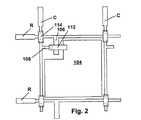
図2からアクティブマトリックス表示装置製造の当業者にとって明らかなように、MEMSスイッチの存在を別にして、図2に示すバックプレーンは、従来のトランジスタベースのアクティブマトリックスバックプレーンに非常によく似ている。バックプレーンは、任意の一時点に行電極Rの1つを選択するように(すなわち、それに印加する動作電圧を有するように)、従来の設計の行ドライバ(図示せず)に接続している複数の並列行電極Rを備え、他の行は通常、図示したバックプレーンから電気光学媒体の反対側に設けられた1つの共通電極と同じ電圧に設定されている。所定の間隔の後、各行電極Rを周期的なやり方で順に選択するように、もともと選択した行電極Rの選択を取り消し、次の行電極Rを選択して、このシーケンスが連続する。バックプレーンはさらに、列電極Cを備える。これらはお互いに並列に延びているが、行電極に、第1の、つまりピクセル電極104に垂直である。このうちの1つだけが図2に図示されている。ピクセル電極104は、各ピクセル電極を、1つの行電極Rと1つの列電極Cとの交差部分に一意に対応付けられるように、矩形のアレイ状に配列されている。ピクセル電極104は、その対応付けられた列電極CにMEMSスイッチを介して接続している。スイッチは、片持ばり112と、アクチュエータ(つまり第2の)電極106(対応付けられた行電極Rが延設した形態を有すると、対応付けられた列電極Cが延設した形態を有するソース(つまり第3の)電極108とを備える。MEMSスイッチに精通している者に明らかなように、アクチュエータ電極106に動作電圧を印加していないと、ソース電極108から間隔をおいた片持ばり112の自由端(図2の左側端)でMEMSスイッチが開いた位置にあるので、このピクセル電極104と対応付けられた列電極Cとの間に電気的接触はない。しかしながら、行ドライバが特定の行を選択して動作電圧を選択した行電極Rに印加すると、動作電圧がアクチュエータ電極106に現れ、その自由端がソース電極108と接触するように片持ばり112が下方に引かれるので、このピクセル電極104と対応付けられた列電極Cとの間に電気的接触が行われ、ピクセル電極104が対応付けられた列電極Cと同じ電圧になる。従って、選択する行のピクセル電極(すなわち、選択した行電極Rに対応付けられた電極)だけが、対応付けられた列電極Cと同じ電圧になって、表示装置に隣接して設けられた電気光学媒体の書き込みが、従来のトランジスタベースのバックプレーンの書き込みと全く同様に、ラインごとのやり方で進められる。 As will be apparent to those skilled in the art of active matrix display manufacturing from FIG. 2, apart from the presence of a MEMS switch, the backplane shown in FIG. 2 is very similar to a conventional transistor-based active matrix backplane. . The backplane is connected to a conventionally designed row driver (not shown) to select one of the row electrodes R at any one time (ie, to have an operating voltage applied to it). A plurality of parallel row electrodes R are provided, and the other rows are usually set to the same voltage as one common electrode provided on the opposite side of the electro-optic medium from the illustrated backplane. After a predetermined interval, the selection of the originally selected row electrode R is canceled and the next row electrode R is selected so that each row electrode R is sequentially selected in a periodic manner, and this sequence continues. The backplane further includes a column electrode C. They extend in parallel to each other but are perpendicular to the row electrodes and to the first or
図2に示すバックプレーンはさらに、各ピクセル電極104に対応付けられたキャパシタ電極114を備え、1つのキャパシタ電極114は列電極Cの隣接する部分とキャパシタを構成する。 The backplane shown in FIG. 2 further includes a
図2に示すバックプレーンの製造プロセスについて、図1A〜図1Dを参照して説明する。図1Aに示すように、プロセスは、例えば高分子フィルムまたは高分子をコーティングした金属箔の絶縁基板102から開始する。プロセスの第1の段階では、任意の都合の良い方法で薄い金属層を基板102に成膜してパターン形成して、3つの電極、すなわちピクセル電極104、”ゲート”つまりアクチュエータ電極106およびソース電極108を形成して、図1Aに示す構造を製造する。プロセスの好ましい形態では、金属層は、金を約100nmの厚さにスパッタで成膜する。次に、犠牲層110を図1Bに示す形態で成膜してアクチュエータおよびソース電極を覆うが、ピクセル電極104は露出したままにしておく。図1Bに示すように、この犠牲層110は部分的に覆うもので、ピクセル電極104とアクチュエータ電極106との間のギャップをすべて覆うものではないことに留意する。犠牲層110を望ましくは、銅を室温で約1μmの厚さにスパッタで成膜する。次に、犠牲層をエッチングして、機械的な片持ばりのベース領域を形成して、金属の2つの基板のキャパシタの支柱をサポートする。フォトレジスト層を追加してパターン形成して、アパーチャを残して、そして片持ばり112およびキャパシタ電極114をメッキする。好ましくは、室温で電気メッキ溶液および金等の低応力材料を用いる(理解しやすいように、図1A〜図1Dのキャパシタ電極114の位置をずらしている)ビーム112の厚さは、望ましくは約2〜4μmである。最後に、フォトレジスト層を剥離して、図1Cに示す構造を形成して、次に、好ましくはウェットエッチングを用いて犠牲層110を除去するので、片持ばり112が遊離する。 2 will be described with reference to FIGS. 1A to 1D. As shown in FIG. 1A, the process begins with an insulating
用いる電気光学媒体の種類によるが、MEMSスイッチと電気光学媒体との間を物理的に分離して維持することは望ましく、あるいは不可欠なことである。この目的のため、保護封止層をバックプレーンに追加して、犠牲層を削除した後でMEMSスイッチが誤って破損しないようにすることもできる。図3に示すように、このような保護封止層の好ましい形態は、MEMSスイッチにそろえられ、基板に接着した、前もってパターン形成したポリイミドまたは他の高分子封止材料116を備える。 Depending on the type of electro-optic medium used, it may be desirable or essential to maintain a physical separation between the MEMS switch and the electro-optic medium. For this purpose, a protective sealing layer can be added to the backplane to prevent accidental breakage of the MEMS switch after the sacrificial layer is removed. As shown in FIG. 3, a preferred form of such a protective sealing layer comprises a pre-patterned polyimide or other
MEMSベースの本発明のバックプレーンにより、重要な技術的利点をいくつか提供する。MEMSスイッチは、”オン”状態では低いインピーダンスで、”オフ”状態では非常に高いインピーダンスになる。従って、優れたオン/オフ比が得られるので、他の種類の非線形要素を通過するリーク電流に伴う問題を回避できる。上述のように図1A〜図1Dを参照して、3つまたは4つのマスクを用い、高温処理工程を全く必要としない簡単なプロセスで、MEMSスイッチを製造することができる。従って、例えば、ポリ(エチレンテレフタレート)フィルムといった、低コストのフレキシブル基板にこのプロセスを用いることができる。また、上記のMEMS製造プロセス薄膜トランジスタまたはダイオードに基づくバックプレーンの製造プロセスよりも、処理中に環境的汚染受ける可能性が低い。これにより、必要とするクリーンルーム設備のコストを低減するようになる。また、MEMSベースのバックプレーンの製造プロセスにより、粗いパターン形成ステップのいくつかを利用できるようになる。 The MEMS-based backplane of the present invention provides several important technical advantages. The MEMS switch has a low impedance in the “on” state and a very high impedance in the “off” state. Therefore, since an excellent on / off ratio can be obtained, problems associated with leakage current passing through other types of nonlinear elements can be avoided. Referring to FIGS. 1A-1D as described above, a MEMS switch can be fabricated with a simple process using three or four masks and requiring no high temperature processing steps. Thus, for example, this process can be used for low cost flexible substrates such as poly (ethylene terephthalate) films. Also, it is less likely to be subject to environmental contamination during processing than the MEMS manufacturing process backplane manufacturing process based on thin film transistors or diodes. Thereby, the cost of the required clean room facility is reduced. Also, the MEMS-based backplane manufacturing process allows some of the rough patterning steps to be utilized.
MEMSスイッチは、ピクセル静電容量に対する非常に細い選択線を有しているので、MEMSベースのバックプレーンは、同様のトランジスタまたはダイオードベースのバックプレーンよりも、このような静電容量によるDC不均衡が小さく、このDC不均衡の低減は、いくつかの種類の電気光学媒体、特に粒子ベースの電気泳動媒体の動作寿命および/または表示装置特性を延長するのに重要である。また、MEMSベースの表示装置における選択線およびデータ線の重複領域が空気で分離できるので(図1Dおよび図2を参照のこと)、空気の比誘電率がほぼ正確に1で、得られる低減した静電容量により、表示装置の消費電力が低減することと、消費電力の大きな部分がデータ線に対応付けられた静電容量の充放電によるので、このような重複領域の単位面積当りの不要の静電容量を絶対最小値にしておける。 MEMS switches have a very narrow selection line for pixel capacitance, so a MEMS-based backplane has a DC imbalance due to such capacitance than a similar transistor or diode-based backplane. This reduction in DC imbalance is important for extending the operating life and / or display characteristics of some types of electro-optic media, particularly particle-based electrophoretic media. In addition, since the overlapping area of the selection line and the data line in the MEMS-based display device can be separated by air (see FIG. 1D and FIG. 2), the relative permittivity of air is almost exactly 1 and reduced. Capacitance reduces the power consumption of the display device, and the large part of the power consumption is due to the charging / discharging of the capacitance associated with the data lines. Capacitance can be set to the absolute minimum.
MEMSベースの本発明のバックプレーンの変更した形態では、図1D、図2および図3に示す片持ばりを、MEMSダイアフラムに置換することもできる。これは、片持ばりよりも静摩擦の影響を受ける可能性が低い。 In a modified form of the MEMS-based backplane of the present invention, the cantilever shown in FIGS. 1D, 2 and 3 can be replaced with a MEMS diaphragm. This is less likely to be affected by static friction than a cantilever.
パートB:本発明のエンボス加工プロセス
すでに述べたように、バックプレーンの製造には、基板上に小型部品のパターン形成を必要とする。表1に示すように、各種のパターン形成の応用例に必要なクリティカルディメンション長さのスケールの範囲があり、これらの寸法を正しく達成するために技術範囲として用いられてきた。Part B: Embossing Process of the Invention As already mentioned, the production of a backplane requires the patterning of small parts on a substrate. As shown in Table 1, there is a range of critical dimension length scales required for various patterning applications, and has been used as a technical scope to achieve these dimensions correctly.

前述のように、本発明の第2の面は、別のパターン形成技術、すなわち、バックプレーンの構成部品および他の電子装置をパターン形成する、エンボス加工レジストプロセスに関する。エンボス加工レジストプロセスにより、従来のフォトリソグラフィプロセスよりも利点をいくつか提供し、高いスループットのロールツーロール処理を可能にし、1μmを下回る部品サイズを可能にし、処理コストの固定費または変動費の低減を可能にする。 As mentioned above, the second aspect of the present invention relates to another patterning technique, namely an embossing resist process for patterning backplane components and other electronic devices. The embossed resist process offers several advantages over traditional photolithography processes, enables high-throughput roll-to-roll processing, enables component sizes below 1 μm, and reduces fixed or variable processing costs Enable.
添付の図面の図4A〜図4Eは、本発明のエンボス加工プロセスを示す。図4Aに示すように、基板402をまず、材料404でコーティングしてパターン形成する。この材料は、金属、絶縁体、半導体または任意の他の種類のパターン形成可能な材料とすることができる。エンボス加工可能な材料層(以下では、便宜上”レジスト”という)406を次に、材料404に塗布して、”マスタスタンプ”(好ましくは、図4Aに示すようなエンボス加工ローラ408の形態である)を用いてレジストをエンボス加工して、レジストをテクスチャまたはパターン形成する。図4Bからよくわかるように、このエンボス加工ステップにより、レジスト406を厚い(第2の)領域406Aと薄い(第1の)領域406Bとに成形し、ローラ408のパターン形成により、任意の所望のやり方で、レジスト406を所定の2つの種類の領域に分離する。 4A-4E of the accompanying drawings illustrate the embossing process of the present invention. As shown in FIG. 4A, a
このプロセスの次のステップでは、薄い領域406Bを除去して基底材料404を十分露出する程度に、パターン形成したレジストをわずかにエッチング(半導体製造技術の当業者に周知の任意の従来のエッチングプロセスを用いて)するが、材料404が厚い領域406Aを覆う部分を残すようにするので、図4Cに示す構造を形成する。次に基板を第2のエッチング工程にかけて、材料404の露出部分を所望の分量エッチングするので、図4Dに示す構造を形成する。最後に、図4Eに示すように、レジストを基板から剥離して、最終的なパターン形成材料404を基板402に残す。 In the next step of this process, the patterned resist is slightly etched to remove the thin regions 406B and sufficiently expose the underlying material 404 (any conventional etching process known to those skilled in the semiconductor manufacturing arts). However, the
表面に塗布したエンボス加工可能な材料を、パターン形成ステップを最適化するように選択することもできる。市販のフォトレジストを、エンボス加工可能な材料として用いることもできる。フォトレジストを、そのガラス転移温度(Tg)を越える温度でエンボス加工することもできるし、ウェットまたはドライエッチングを行って基底材料を露出することもできる。レジストを、基底材料のエッチングに用いる化学薬品に耐性のものを選択することもできるし、基底材料のパターン形成後にその表面から容易に剥離するものを選択することもできる。ある場合では、レジストをエンボス加工する前にレジストを”ソフトベーク”して溶剤を除去することは必要または望ましいことである。また、ある場合では、エッチングして薄い領域406Bを除去した後、基底材料のエッチングにレジストが確実に耐えることができるように、レジストを”ハードベーク”することは好ましいことである。The embossable material applied to the surface can also be selected to optimize the patterning step. Commercially available photoresist can also be used as a material that can be embossed. The photoresist can be embossed at a temperature above its glass transition temperature (Tg ), or wet or dry etching can be performed to expose the base material. It is possible to select a resist that is resistant to chemicals used for etching the base material, or a resist that easily peels from the surface after patterning of the base material. In some cases, it may be necessary or desirable to “soft bake” the resist to remove the solvent before embossing the resist. In some cases, it may also be desirable to “hard bake” the resist after etching to remove the thin regions 406B so that the resist can reliably withstand the etching of the base material.
溶融材料(高分子または別のもの)を、エンボス加工可能な材料またはレジストとして用いることもできる。例えば、ろう状材料(例えば、オクタコサン、ノナデカン等のアルカン等)を用いることもできる。これらのろう状材料を、加熱スロットダイ、凹版、スピンコーティングチャック、オフセット印刷ローラ、またはこの分野の当業者が周知の他の同様の装置を用いて、液相でコーティングすることもできる。溶融材料は通常成膜すると、薄い、エンボス加工可能なフィルム状に固化し、次にウェットまたはドライエッチング技術を用いて、エンボス加工しエッチバックすることもできる。パターン形成したレジスト膜は、基底材料のエッチングマスクとしての役割を果たし、すでに述べたように、基底材料のエッチングに続いて剥離する。ヘキサン等の溶剤は、前述のろう状材料を効果的に剥離するので、このようなプロセスには利点がある。成膜後にレジストから溶剤を乾燥させる必要がないからである。また、用いる化学薬品を適切に選択する(”最適化する”)ことにより、パターン形成が完了した後、比較的非毒性の溶剤を用いて、ろう状材料を基底材料から剥離することもできる。 A molten material (polymer or another) can also be used as the embossable material or resist. For example, a wax-like material (for example, alkane such as octacosan and nonadecane) can be used. These waxy materials can also be coated in the liquid phase using a heated slot die, intaglio, spin coating chuck, offset printing roller, or other similar apparatus known to those skilled in the art. Once the molten material is deposited, it can be solidified into a thin, embossable film and then embossed and etched back using wet or dry etching techniques. The patterned resist film serves as an etching mask for the base material, and as described above, the resist film is peeled off after the base material is etched. Such a process is advantageous because solvents such as hexane effectively strip the aforementioned waxy material. This is because it is not necessary to dry the solvent from the resist after film formation. It is also possible to exfoliate the waxy material from the base material using a relatively non-toxic solvent after patterning is completed by appropriate selection of chemicals to be used ("optimize").
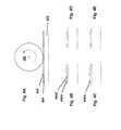
エンボス加工レジストの発想に最適化した重合体を用いることもできる。例えば、図5Aに示す4−水酸化スチレンおよびブチル−メタクリレート重合体である。このブロック共重合体の4−ヒドロキシスチレンの成分は塩基可溶性で、共重合体は酸の存在下で非ブロック化する。その結果、共重合体は、エンボス加工レジストプロセスで有益な特性をいくつか示す。第一に、高分子の分子量を調整することにより、そのガラス転移温度を約100から約150℃の範囲内に調整することができるので、許容できるエンボス加工温度範囲になる。第二に、弱塩基溶液を用いてパターン形成した共重合体をエッチバックすることもできるので、基底材料を露出する。最も普通の基底材料(金属,半導体、絶縁体)をエッチングするのに用いる酸は、基底材料のエッチングの間に共重合体を非ブロック化するので、エッチングが完了した後、レジストを容易に除去することができる。 Polymers optimized for the concept of embossed resist can also be used. For example, 4-hydroxystyrene and butyl-methacrylate polymers shown in FIG. 5A. The 4-hydroxystyrene component of this block copolymer is base soluble and the copolymer is deblocked in the presence of acid. As a result, the copolymer exhibits some beneficial properties in the embossed resist process. First, by adjusting the molecular weight of the polymer, its glass transition temperature can be adjusted within the range of about 100 to about 150 ° C., thus providing an acceptable embossing temperature range. Second, the base material is exposed because the patterned copolymer can be etched back using a weak base solution. The acid used to etch the most common base materials (metals, semiconductors, insulators) deblocks the copolymer during the base material etch, so the resist is easily removed after the etch is complete can do.
あるいは、エンボス加工レジスト共重合体で、図5Bに示すメタクリレートベースのブロックを、図5Aに示すブチルメタクリレートブロックの代わりに用いることもできる。この異なるブロックを用いることにより、エンボス加工レジストを約175〜180℃の温度で熱によって非ブロック化することができる。基底材料のパターン形成を上記のように従来の酸性エッチング化学薬品を用いないでエッチングを行う場合に、熱による非ブロック化は、有用な別の方法である。 Alternatively, in an embossed resist copolymer, the methacrylate-based block shown in FIG. 5B can be used in place of the butyl methacrylate block shown in FIG. 5A. By using this different block, the embossed resist can be deblocked by heat at a temperature of about 175-180 ° C. Deblocking with heat is another useful method when patterning the base material is etched without using conventional acidic etching chemicals as described above.
本発明のプロセスのエンボス加工処理に用いられるマスタスタンプを、様々な従来技術の超微細加工技術を用いて形成することもできる。好ましくは、マスタスタンプは、コンパクトディスク製造業者がコンパクトディスク(CD)やDVDの製造に用いるニッケルマスタスタンプの作成に一般的に利用する技術を用いて作成する。これらの技術には、ニッケルマスタスタンプの電鋳に対して、フォトリソグラフィで形成した鋳型の作成が必要である。 The master stamp used in the embossing process of the process of the present invention can also be formed using various conventional ultra-fine processing techniques. Preferably, the master stamp is created using a technique commonly used by a compact disc manufacturer to create a nickel master stamp for use in the production of a compact disc (CD) or DVD. These techniques require the creation of a mold formed by photolithography in contrast to nickel master stamp electroforming.
CDおよびDVDのマスタリングプロセスから得られるニッケル箔は、本発明に用いるのに非常に適しているが、従来のCD/DVDプロセスのいくつかを変更する必要がある。まず、CD上のピットは通常、250nmより浅いが、約1〜10μm深さのマスタスタンプ上に部品を作成するには通常望ましいものの、本発明では、優れた刻印を形成するには、スタンプ部品はレジスト厚さの約2〜5倍必要で、通常約100〜1000nmになる。 Nickel foils obtained from CD and DVD mastering processes are very suitable for use in the present invention, but some of the conventional CD / DVD processes need to be modified. First, the pits on a CD are usually shallower than 250 nm, but it is usually desirable to make a part on a master stamp of about 1-10 μm depth, but in the present invention, a stamp part is used to form an excellent stamp. Requires about 2 to 5 times the resist thickness, and is usually about 100 to 1000 nm.
このような深さの部品をマスタ上に作成するには、マスタ製造は、厚い膜処理に最適化したフォトレジストを用いる必要がある。例えば、SU−8レジストを用いて、100μm以上もの厚さの膜を形成することもできる。ニッケルマスタをその鋳型から確実に簡単に外すために、傾斜を付けた側壁をマスタの部品部分に形成することが好ましい。傾斜側壁の技術を、高スループット薬品検出システムを繰り返すために用いるマスタの形成に利用していたが、エンボス加工レジストプロセスには明らかに用いられていなかった。 In order to produce a part having such a depth on the master, the master manufacturing needs to use a photoresist optimized for thick film processing. For example, a film having a thickness of 100 μm or more can be formed using SU-8 resist. In order to ensure that the nickel master is easily removed from its mold, it is preferable to form an inclined side wall in the part of the master. The slanted sidewall technique was used to form a master that was used to repeat the high-throughput drug detection system, but was not clearly used in the embossed resist process.
マスタスタンプの幾何学的機能として、別の技術、高度化MEMS装置の製造に従来から行われているように、例えば、反応性イオンエッチング(RIE)またはレーザアブレーションを用いてシリコンウェハまたはガラス基板を所望の部品を有するようにエッチングすることは有益である。 As a geometrical function of the master stamp, a silicon wafer or glass substrate can be formed using, for example, reactive ion etching (RIE) or laser ablation, as is conventionally done in the manufacture of other technologies, advanced MEMS devices. It is beneficial to etch to have the desired part.
本発明のエンボス加工プロセスにより、材料のパターン形成について、従来のフォトリソグラフィ技術よりも明らかな利点をいくつか提供する。エンボス加工プロセスにより、リソグラフィよりも低い固定費および変動費が見込まれるのは、従来のリソグラフィ用紫外線露光装置を機械的エンボス加工装置に置き換え、従来のフォトレジストを安価な化学的に単純な材料と置き換えるからである。本発明のエンボス加工プロセスは、部品の特徴的な寸法を6〜10nmという小ささで達成できることを示している。これは、高度のフォトリソグラフィプロセスで達成可能なものよりも5〜10倍小さい。溶融高分子レジストを利用する本発明の実施の形態を用いる場合、フォトリソグラフィに必要なソフトベークステップおよびハードベークステップを完全に省くことができる。ミクロンスケールに小さくなる部品サイズでは、オールウェットプロセスを用いてエンボス加工レジストプロセスを正常に完了することもできる。すなわち、高価な真空ステップを全く必要としない。最後に、エンボス加工レジストプロセスは、図4Aに示すように、マスタスタンプとしてローラを用いる高スループットのロールツーロールパターン形成に非常に適している。 The embossing process of the present invention provides several distinct advantages over conventional photolithography techniques for patterning materials. The embossing process is expected to have lower fixed and variable costs than lithography, replacing conventional lithography UV exposure equipment with mechanical embossing equipment and replacing traditional photoresists with cheap, chemically simple materials. It is because it replaces. The embossing process of the present invention shows that the characteristic dimensions of parts can be achieved as small as 6-10 nm. This is 5 to 10 times smaller than that achievable with advanced photolithography processes. When using an embodiment of the present invention that utilizes a molten polymer resist, the soft and hard bake steps required for photolithography can be omitted completely. For part sizes down to micron scale, the embossing resist process can also be successfully completed using an all wet process. That is, no expensive vacuum steps are required. Finally, the embossing resist process is well suited for high throughput roll-to-roll pattern formation using a roller as a master stamp, as shown in FIG. 4A.
パートC:埋込みトランジスタバックプレーン
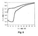
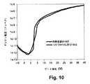
前述のように、電気光学表示装置の製造において、表示装置のバックプレーンおよび前面部は通常、別々の装置として製造して、共に積層して、最終的な表示装置を作成する。このような積層は通常、積層用接着剤を用いて、バックプレーンを表示装置の前面部に接着する必要がある。従って、最終的な表示装置では、製造したバックプレーンの露出表面が積層用接着剤に対し露出する。多くの場合、積層用接着剤には、バックプレーンの露出表面上のトランジスタまたは他の非線形装置の性能に有害となるような影響を与える材料が含まれている。例えば、特定の市販のポリウレタン積層用接着剤をアモルファスシリコンTFTのチャネルに直接塗布すると、トランジスタを完全に破壊してしまうことがわかっている。添付の図面の図6に示すように、このようなある実験では、トランジスタのオン/オフ比が106から約10に低減したことがわかった。また、ある種類の電気光学媒体は流動化学種を含んでいて、これは、積層用接着剤を移動可能でトランジスタまたは他の非線形装置に悪影響を与えることになる。例えば、粒子ベースの電気泳動媒体は、炭化水素溶剤を含み、これは、このように移動可能で、アモルファスシリコントランジスタの特性に悪影響を与えることもある。最後に、アモルファスシリコンTFTはまたTFTに電気光学媒体を介して侵入する光や水分により、劣化することもある。封止粒子ベースの電気泳動媒体等の多くの電気光学媒体は通常不透光であると考えられているが、ある種の光は、例えばカプセルの間の小さなギャップを介して、このような媒体を通過するものもある。Part C: Embedded Transistor Backplane As mentioned above, in the manufacture of electro-optic display devices, the backplane and front part of the display device are usually manufactured as separate devices and stacked together to produce the final display device. create. In such a lamination, it is usually necessary to bond the backplane to the front surface portion of the display device using a lamination adhesive. Therefore, in the final display device, the exposed surface of the manufactured backplane is exposed to the laminating adhesive. In many cases, the laminating adhesive includes materials that have a detrimental effect on the performance of transistors or other non-linear devices on the exposed surface of the backplane. For example, it has been found that applying certain commercially available polyurethane laminating adhesives directly to the channel of an amorphous silicon TFT completely destroys the transistor. As shown in FIG. 6 of the accompanying drawings, it was found that in one such experiment, the transistor on / off ratio was reduced from 106 to about 10. Also, certain types of electro-optic media contain flowing chemical species that can move the laminating adhesive and adversely affect transistors or other non-linear devices. For example, particle-based electrophoretic media include a hydrocarbon solvent, which can move in this way and can adversely affect the properties of the amorphous silicon transistor. Finally, amorphous silicon TFTs can also be degraded by light and moisture entering the TFTs via electro-optic media. Many electro-optic media, such as encapsulated particle-based electrophoretic media, are usually considered opaque, but certain types of light can pass through such media, for example, through small gaps between the capsules. Some pass through.
このような問題を回避するために、非線形装置と電気光学媒体との間にバリア層またはパッシベーション層を介在させることが知られている。例えば、前述の2002/0119584号には、いわゆる”埋込みトランジスタ設計”のバックプレーンが記載されている。このような設計では、積層の前に、ピクセル電極だけが最終的なバックプレーンに露出する。バックプレーンのトランジスタは、パッシベーション層の下に”埋め込まれて”いて、トランジスタのドレインは、パッシベーション層を貫通する導電性バイアにより、それらに対応付けられたピクセル電極に接続している。前述の公開出願に記載されているこの設計の好ましい形態では、パッシベーション層は、プラズマ促進化学蒸(PECVD)で成膜した、約5μmを越える窒化ケイ素を備える。この比較的厚い層により、トランジスタのチャネルとデータ線とを覆う必要がある。クラックをまったく発生させることなくこのような厚い窒化物層を成膜することは困難である。従って、パッシベーション層としての窒化ケイ素と置換する別の材料を発見することが望ましい。 In order to avoid such a problem, it is known to interpose a barrier layer or a passivation layer between the nonlinear device and the electro-optic medium. For example, the aforementioned 2002/0119584 describes a so-called “buried transistor design” backplane. In such a design, only the pixel electrodes are exposed to the final backplane prior to lamination. The backplane transistors are “buried” under the passivation layer, and the drains of the transistors are connected to their associated pixel electrodes by conductive vias that penetrate the passivation layer. In a preferred form of this design described in the aforementioned published application, the passivation layer comprises more than about 5 μm silicon nitride deposited by plasma enhanced chemical vapor (PECVD). This relatively thick layer needs to cover the channel and data lines of the transistor. It is difficult to form such a thick nitride layer without generating any cracks. Therefore, it is desirable to find another material that replaces silicon nitride as a passivation layer.
エポキシ、ポリウレタン、シリコン、ポリアクリレートおよびポリイミドポリマーをパッシベーション層としての窒化ケイ素の代わりとして用いて、電気光学表示装置に用いられるバックプレーンのトランジスタまたは他の非線形装置を封止して保護できることがわかっている。好ましいポリマーは、スクリーン印刷によりバックプレーンに塗布することができる。これは、PECVDよりも複雑でなく、より少ない設備ですむプロセスである。 It has been found that epoxy, polyurethane, silicon, polyacrylate and polyimide polymers can be used in place of silicon nitride as a passivation layer to seal and protect backplane transistors or other nonlinear devices used in electro-optic displays. Yes. Preferred polymers can be applied to the backplane by screen printing. This is a process that is less complex and requires less equipment than PECVD.
本発明で用いる高分子封止材料は、熱または放射線、好ましくは紫外線放射のいずれかで硬化可能である。好ましい熱硬化性材料として、エポキシテクノロジ(Epoxy Technology)社製エポテック(EpoTek)H70E−2LCと、デュポンエレクトロニックマテリアルズ社製デュポン(DuPont)5036とが含まれる。好ましい紫外線硬化材料として、アライドフォトケミカル(Allied Photochemical Inc)社製TGH1003×2と、クリエーティブマテリアルズ(Creative Materials Inc)社製CM116−20とが含まれる。これらの材料の特性および硬化条件について、以下の表2にまとめている。 The polymeric sealing material used in the present invention can be cured by either heat or radiation, preferably ultraviolet radiation. Preferred thermosetting materials include EpoTek H70E-2LC from Epoxy Technology and
図7〜図10は、上記の表2に記載の材料がすべて要項な結果であったことを示している。デュポン5036で封止した後は、オフ電流が低下している。封止材料としてエポテックH70E−2LCを用いる場合は、TFTの性能は同じである。TGH1003×2をコーティングしたTFTは、制御装置と比較して、同じ性能であった。CM116−20で封止されているTFTは、制御装置よりも良いサブスレショルド勾配である。しかしながら、図11および図12には、間違った封止材料を選択すると何が起きるが示されている。図11は、エポテックH62で封止した場合は、アモルファスシリコンTFTがほとんど破壊されたことを示し、図12は、エレゥトロダッグ452SSで封止した場合はTFTが劣化して、TFTが高いオフ電流でリークしやすくなることが示している。 7 to 10 show that all the materials shown in Table 2 above are essential results. After sealing with
本発明は従って、電気光学表示装置のバックプレーンに用いられるトランジスタおよび他の非線形装置を保護する低コストのプロセスを提供する。用いる高分子封止材料を、スクリーン印刷で成膜してパターン形成する。上述の従来技術のプロセスで用いられるPECVD窒化ケイ素成膜およびフォトリソグラフィパターン形成プロセスと比較して、低コストのプロセスである。 The present invention thus provides a low cost process for protecting transistors and other nonlinear devices used in the backplane of electro-optic display devices. The polymer sealing material to be used is formed into a pattern by screen printing. Compared to the PECVD silicon nitride deposition and photolithography patterning process used in the above prior art processes, it is a low cost process.
本発明の各種の面について、封止粒子ベースの電気泳動媒体と共に用いることについて主に説明してきたが、上述の任意の種類の電気光学媒体を、本発明の電気光学表示装置に用いることができることが理解されるであろう。 The various aspects of the present invention have been mainly described for use with encapsulating particle-based electrophoretic media, but any of the above-described electro-optic media can be used in the electro-optic display device of the present invention. Will be understood.
Claims (22)
Translated fromJapanese少なくとも1つの光学的特性が異なる第1および第2の表示装置状態を有する電気光学媒体の層であって、媒体に対する電界の印加によりその第1の表示装置状態から第2の表示装置状態へ変化可能な電気光学媒体と、
電気光学媒体の層と隣接して配置されたバックプレーンであって、電圧を印加することにより、電気光学媒体に電界を印加するように配列されたピクセル電極(104)と、電圧をピクセル電極(104)に供給するように配列された電圧供給線(C)とをさらに備えるバックプレーンとを備え、
電気光学表示装置は、電圧供給線(C)とピクセル電極(104)との間に配置されたマイクロメカニカルスイッチ(106、112)を特徴とし、マイクロメカニカルスイッチ(106、112)は、開状態では電圧供給線(C)をピクセル電極(104)に電気的に接続せず、閉状態では電圧供給線(C)をピクセル電極(104)に電気的に接続することを特徴とする。An electro-optical display device comprising:
A layer of an electro-optic medium having first and second display device states having at least one different optical characteristic, wherein the layer changes from the first display device state to the second display device state by applying an electric field to the medium. Possible electro-optic medium,
A backplane disposed adjacent to the layer of electro-optic medium, the pixel electrode (104) arranged to apply an electric field to the electro-optic medium by applying a voltage, and the voltage to the pixel electrode ( 104) and a backplane further comprising a voltage supply line (C) arranged to supply to
The electro-optic display device is characterized by a micromechanical switch (106, 112) disposed between the voltage supply line (C) and the pixel electrode (104), and the micromechanical switch (106, 112) is in the open state. The voltage supply line (C) is not electrically connected to the pixel electrode (104), and the voltage supply line (C) is electrically connected to the pixel electrode (104) in the closed state.
第1の電極(108)、第2の電極(106)および第3の(104)電極を間隔をおいて基板(102)に形成して、
その後、犠牲層(110)を基板(102)に形成して、犠牲層(110)は第1の電極(108)および第2の(106)電極を覆うが、少なくとも第3の電極(104)の一部を露出したままにして、
その後、第3の電極(104)の露出部分と接触する第1の部分と、少なくとも第2の電極(106)および第1の電極(108)それぞれの一部に延長するように犠牲層(110)に延設した第2の部分とを有する片持ばり部材(112)を形成するように、導電材料を基板に成膜して、
その後、犠牲層(110)を除去することにより、第2の電極(106)に印加する電圧の影響下で、片持ばり部材(112)の第2の部分が、自在に第1の電極(108)と接触するようになる。A process for forming a backplane for an electro-optic display device, characterized by:
Forming a first electrode (108), a second electrode (106) and a third (104) electrode on the substrate (102) at an interval;
Thereafter, a sacrificial layer (110) is formed on the substrate (102), and the sacrificial layer (110) covers the first electrode (108) and the second (106) electrode, but at least the third electrode (104). Leave a part of
Thereafter, the sacrificial layer (110) extends to a first portion in contact with the exposed portion of the third electrode (104) and at least a portion of each of the second electrode (106) and the first electrode (108). A conductive material is deposited on the substrate so as to form a cantilever member (112) having a second portion extending to
Thereafter, the sacrificial layer (110) is removed, so that the second portion of the cantilever member (112) can freely move under the influence of the voltage applied to the second electrode (106). 108).
基板(402)に、少なくとも1つの電子構成部品を形成可能な構成部品材料(404)の層を形成して、
エンボス加工可能な材料の層(406)を構成部品材料の層(404)に形成して、
エンボス加工可能な材料の層(406)をイメージ的にエンボス加工して、少なくとも1つの第1の部分(406B)と、少なくとも1つの第1の部分(406B)よりも厚みが厚い少なくとも1つの第2の部分(406A)とを形成して、
エンボス加工可能な材料(406)をエッチングして、その少なくとも1つの第1の部分(406B)を除去して、その少なくとも1つの第2の部分(406A)に存在するエンボス加工可能な材料を残すことにより、エンボス加工可能な材料の少なくとも1つの第1の部分(406B)の下にある構成部品材料(404)を露出して、
その後、構成部品材料の露出部分(404)をエッチングすることにより、構成部品材料の層をパターン形成して、その中に少なくとも1つの電子構成部品を形成する。A process for forming at least one electronic component of an electronic circuit on a substrate (402), the process characterized by:
Forming a layer of component material (404) on the substrate (402) capable of forming at least one electronic component;
Forming a layer of embossable material (406) on the layer of component material (404);
The embossable material layer (406) is imagewise embossed to provide at least one first portion (406B) and at least one first portion (406B) thicker than the at least one first portion (406B). 2 part (406A),
The embossable material (406) is etched to remove its at least one first portion (406B), leaving the embossable material present in the at least one second portion (406A). Thereby exposing the component material (404) under the at least one first portion (406B) of the embossable material;
Thereafter, the exposed portion (404) of the component material is etched to pattern the component material layer to form at least one electronic component therein.
基板と、
基板に形成したトランジスタと、
トランジスタを覆うパッシベーション層と、
トランジスタからパッシベーション層の反対側に設けられたピクセル電極と、
パッシベーション層を貫通して、トランジスタをピクセル電極に電気的に接続する導電性バイアとを備え、
バックプレーンは、パッシベーション層が、エポキシ、ポリウレタン、シリコンポリアクリレートおよびポリイミドポリマーからなる基から選択する高分子を含むことを特徴とする。A backplane for an electro-optic display device, comprising:
A substrate,
A transistor formed on a substrate;
A passivation layer covering the transistor;
A pixel electrode provided on the opposite side of the passivation layer from the transistor;
A conductive via that penetrates the passivation layer and electrically connects the transistor to the pixel electrode;
The backplane is characterized in that the passivation layer comprises a polymer selected from the group consisting of epoxy, polyurethane, silicon polyacrylate and polyimide polymer.
少なくとも1つの光学的特性が異なる第1および第2の表示装置状態を有する電気光学媒体の層であって、媒体への電界の印加により、その第1の表示装置状態から第2の表示装置状態へ変更可能な電気光学媒体と、
電気光学媒体層に隣接して配置され、電圧をそのピクセル電極に印加することにより、電界を電気光学媒体へ印加するように配置した請求項19乃至21に記載のバックプレーン。An electro-optical display device comprising:
A layer of an electro-optic medium having first and second display device states having at least one different optical characteristic, wherein the first display device state is changed to the second display device state by applying an electric field to the medium. A changeable electro-optic medium,
22. A backplane according to any one of claims 19 to 21 arranged adjacent to the electro-optic medium layer and arranged to apply an electric field to the electro-optic medium by applying a voltage to its pixel electrode.
Applications Claiming Priority (2)
| Application Number | Priority Date | Filing Date | Title |
|---|---|---|---|
| US31978602P | 2002-12-16 | 2002-12-16 | |
| PCT/US2003/040257WO2004059378A2 (en) | 2002-12-16 | 2003-12-16 | Backplanes for electro-optic displays |
Related Child Applications (1)
| Application Number | Title | Priority Date | Filing Date |
|---|---|---|---|
| JP2009262388ADivisionJP2010044420A (en) | 2002-12-16 | 2009-11-17 | Backplane for electro-optic display |
Publications (1)
| Publication Number | Publication Date |
|---|---|
| JP2006510066Atrue JP2006510066A (en) | 2006-03-23 |
Family
ID=32680696
Family Applications (3)
| Application Number | Title | Priority Date | Filing Date |
|---|---|---|---|
| JP2004563695APendingJP2006510066A (en) | 2002-12-16 | 2003-12-16 | Backplane for electro-optic display |
| JP2009262388APendingJP2010044420A (en) | 2002-12-16 | 2009-11-17 | Backplane for electro-optic display |
| JP2011231163AWithdrawnJP2012014204A (en) | 2002-12-16 | 2011-10-20 | Backplane for electro-optical display device |
Family Applications After (2)
| Application Number | Title | Priority Date | Filing Date |
|---|---|---|---|
| JP2009262388APendingJP2010044420A (en) | 2002-12-16 | 2009-11-17 | Backplane for electro-optic display |
| JP2011231163AWithdrawnJP2012014204A (en) | 2002-12-16 | 2011-10-20 | Backplane for electro-optical display device |
Country Status (7)
| Country | Link |
|---|---|
| US (2) | US7365733B2 (en) |
| EP (1) | EP1573389B1 (en) |
| JP (3) | JP2006510066A (en) |
| KR (2) | KR100937613B1 (en) |
| CN (2) | CN1726428A (en) |
| AU (1) | AU2003299673A1 (en) |
| WO (1) | WO2004059378A2 (en) |
Cited By (9)
| Publication number | Priority date | Publication date | Assignee | Title |
|---|---|---|---|---|
| JP2009122144A (en)* | 2007-11-09 | 2009-06-04 | Seiko Epson Corp | Active matrix device, electro-optical display device, and electronic apparatus |
| JP2009122143A (en)* | 2007-11-09 | 2009-06-04 | Seiko Epson Corp | Active matrix device, electro-optical display device, and electronic apparatus |
| JP2009134256A (en)* | 2007-11-09 | 2009-06-18 | Seiko Epson Corp | Active matrix device, switching element manufacturing method, electro-optical display device, and electronic apparatus |
| JP2010224396A (en)* | 2009-03-25 | 2010-10-07 | Seiko Epson Corp | Electro-optical device and driving method thereof, switch and manufacturing method thereof, and electronic apparatus |
| JP2010224397A (en)* | 2009-03-25 | 2010-10-07 | Seiko Epson Corp | Electro-optical device and driving method thereof, switch and manufacturing method thereof, and electronic apparatus |
| JP2010231169A (en)* | 2009-08-26 | 2010-10-14 | Seiko Epson Corp | Electro-optical device and electronic apparatus |
| US8223285B2 (en) | 2007-11-09 | 2012-07-17 | Seiko Epson Corporation | Active matrix device, method for manufacturing switching element, electro-optical display device, and electronic apparatus |
| JP2014056244A (en)* | 2013-10-02 | 2014-03-27 | Seiko Epson Corp | Electro-optic device and electronic equipment |
| TWI631406B (en)* | 2015-01-05 | 2018-08-01 | 美商電子墨水股份有限公司 | Photoelectric display |
Families Citing this family (294)
| Publication number | Priority date | Publication date | Assignee | Title |
|---|---|---|---|---|
| US7999787B2 (en) | 1995-07-20 | 2011-08-16 | E Ink Corporation | Methods for driving electrophoretic displays using dielectrophoretic forces |
| US7411719B2 (en) | 1995-07-20 | 2008-08-12 | E Ink Corporation | Electrophoretic medium and process for the production thereof |
| US7193625B2 (en) | 1999-04-30 | 2007-03-20 | E Ink Corporation | Methods for driving electro-optic displays, and apparatus for use therein |
| US7848006B2 (en) | 1995-07-20 | 2010-12-07 | E Ink Corporation | Electrophoretic displays with controlled amounts of pigment |
| US7327511B2 (en) | 2004-03-23 | 2008-02-05 | E Ink Corporation | Light modulators |
| US8139050B2 (en) | 1995-07-20 | 2012-03-20 | E Ink Corporation | Addressing schemes for electronic displays |
| US7583251B2 (en) | 1995-07-20 | 2009-09-01 | E Ink Corporation | Dielectrophoretic displays |
| US8040594B2 (en) | 1997-08-28 | 2011-10-18 | E Ink Corporation | Multi-color electrophoretic displays |
| DE69920228T2 (en) | 1998-07-08 | 2005-01-27 | E-Ink Corp., Cambridge | METHOD FOR IMPROVING COLOR REPRODUCTION IN ELECTROPHORETIC DEVICES USING MICROCAPSULES |
| US7119772B2 (en) | 1999-04-30 | 2006-10-10 | E Ink Corporation | Methods for driving bistable electro-optic displays, and apparatus for use therein |
| US8115729B2 (en) | 1999-05-03 | 2012-02-14 | E Ink Corporation | Electrophoretic display element with filler particles |
| US7119759B2 (en) | 1999-05-03 | 2006-10-10 | E Ink Corporation | Machine-readable displays |
| US8009348B2 (en) | 1999-05-03 | 2011-08-30 | E Ink Corporation | Machine-readable displays |
| US7893435B2 (en) | 2000-04-18 | 2011-02-22 | E Ink Corporation | Flexible electronic circuits and displays including a backplane comprising a patterned metal foil having a plurality of apertures extending therethrough |
| AU2002250304A1 (en) | 2001-03-13 | 2002-09-24 | E Ink Corporation | Apparatus for displaying drawings |
| US8390918B2 (en) | 2001-04-02 | 2013-03-05 | E Ink Corporation | Electrophoretic displays with controlled amounts of pigment |
| US7679814B2 (en) | 2001-04-02 | 2010-03-16 | E Ink Corporation | Materials for use in electrophoretic displays |
| US20050156340A1 (en) | 2004-01-20 | 2005-07-21 | E Ink Corporation | Preparation of capsules |
| US7230750B2 (en) | 2001-05-15 | 2007-06-12 | E Ink Corporation | Electrophoretic media and processes for the production thereof |
| US7535624B2 (en)* | 2001-07-09 | 2009-05-19 | E Ink Corporation | Electro-optic display and materials for use therein |
| US7110163B2 (en) | 2001-07-09 | 2006-09-19 | E Ink Corporation | Electro-optic display and lamination adhesive for use therein |
| US6982178B2 (en) | 2002-06-10 | 2006-01-03 | E Ink Corporation | Components and methods for use in electro-optic displays |
| US7952557B2 (en) | 2001-11-20 | 2011-05-31 | E Ink Corporation | Methods and apparatus for driving electro-optic displays |
| US8125501B2 (en) | 2001-11-20 | 2012-02-28 | E Ink Corporation | Voltage modulated driver circuits for electro-optic displays |
| US9412314B2 (en) | 2001-11-20 | 2016-08-09 | E Ink Corporation | Methods for driving electro-optic displays |
| US7528822B2 (en) | 2001-11-20 | 2009-05-05 | E Ink Corporation | Methods for driving electro-optic displays |
| US8558783B2 (en) | 2001-11-20 | 2013-10-15 | E Ink Corporation | Electro-optic displays with reduced remnant voltage |
| US9530363B2 (en) | 2001-11-20 | 2016-12-27 | E Ink Corporation | Methods and apparatus for driving electro-optic displays |
| US8593396B2 (en) | 2001-11-20 | 2013-11-26 | E Ink Corporation | Methods and apparatus for driving electro-optic displays |
| US7190008B2 (en) | 2002-04-24 | 2007-03-13 | E Ink Corporation | Electro-optic displays, and components for use therein |
| US7223672B2 (en) | 2002-04-24 | 2007-05-29 | E Ink Corporation | Processes for forming backplanes for electro-optic displays |
| US8363299B2 (en) | 2002-06-10 | 2013-01-29 | E Ink Corporation | Electro-optic displays, and processes for the production thereof |
| US9470950B2 (en) | 2002-06-10 | 2016-10-18 | E Ink Corporation | Electro-optic displays, and processes for the production thereof |
| US7554712B2 (en) | 2005-06-23 | 2009-06-30 | E Ink Corporation | Edge seals for, and processes for assembly of, electro-optic displays |
| US7843621B2 (en) | 2002-06-10 | 2010-11-30 | E Ink Corporation | Components and testing methods for use in the production of electro-optic displays |
| US7649674B2 (en)* | 2002-06-10 | 2010-01-19 | E Ink Corporation | Electro-optic display with edge seal |
| US7110164B2 (en) | 2002-06-10 | 2006-09-19 | E Ink Corporation | Electro-optic displays, and processes for the production thereof |
| US7583427B2 (en) | 2002-06-10 | 2009-09-01 | E Ink Corporation | Components and methods for use in electro-optic displays |
| US8049947B2 (en) | 2002-06-10 | 2011-11-01 | E Ink Corporation | Components and methods for use in electro-optic displays |
| US20080024482A1 (en) | 2002-06-13 | 2008-01-31 | E Ink Corporation | Methods for driving electro-optic displays |
| US7839564B2 (en) | 2002-09-03 | 2010-11-23 | E Ink Corporation | Components and methods for use in electro-optic displays |
| EP3056941B1 (en) | 2002-09-03 | 2019-01-09 | E Ink Corporation | Electro-phoretic medium |
| US20130063333A1 (en) | 2002-10-16 | 2013-03-14 | E Ink Corporation | Electrophoretic displays |
| US6987603B2 (en) | 2003-01-31 | 2006-01-17 | E Ink Corporation | Construction of electrophoretic displays |
| US7417782B2 (en) | 2005-02-23 | 2008-08-26 | Pixtronix, Incorporated | Methods and apparatus for spatial light modulation |
| US7339715B2 (en) | 2003-03-25 | 2008-03-04 | E Ink Corporation | Processes for the production of electrophoretic displays |
| US7910175B2 (en)* | 2003-03-25 | 2011-03-22 | E Ink Corporation | Processes for the production of electrophoretic displays |
| CN100399109C (en) | 2003-03-27 | 2008-07-02 | 伊英克公司 | Electro-optical components |
| US10726798B2 (en) | 2003-03-31 | 2020-07-28 | E Ink Corporation | Methods for operating electro-optic displays |
| US8174490B2 (en) | 2003-06-30 | 2012-05-08 | E Ink Corporation | Methods for driving electrophoretic displays |
| WO2005010598A2 (en) | 2003-07-24 | 2005-02-03 | E Ink Corporation | Electro-optic displays |
| EP1656658A4 (en) | 2003-08-19 | 2009-12-30 | E Ink Corp | Methods for controlling electro-optic displays |
| WO2005029458A1 (en) | 2003-09-19 | 2005-03-31 | E Ink Corporation | Methods for reducing edge effects in electro-optic displays |
| US20070002009A1 (en)* | 2003-10-07 | 2007-01-04 | Pasch Nicholas F | Micro-electromechanical display backplane and improvements thereof |
| CN101930118B (en) | 2003-10-08 | 2013-05-29 | 伊英克公司 | Electro-wetting displays |
| US8319759B2 (en) | 2003-10-08 | 2012-11-27 | E Ink Corporation | Electrowetting displays |
| US8177942B2 (en) | 2003-11-05 | 2012-05-15 | E Ink Corporation | Electro-optic displays, and materials for use therein |
| US7672040B2 (en)* | 2003-11-05 | 2010-03-02 | E Ink Corporation | Electro-optic displays, and materials for use therein |
| EP2487674B1 (en) | 2003-11-05 | 2018-02-21 | E Ink Corporation | Electro-optic displays |
| US7551346B2 (en)* | 2003-11-05 | 2009-06-23 | E Ink Corporation | Electro-optic displays, and materials for use therein |
| US20110164301A1 (en) | 2003-11-05 | 2011-07-07 | E Ink Corporation | Electro-optic displays, and materials for use therein |
| US8928562B2 (en) | 2003-11-25 | 2015-01-06 | E Ink Corporation | Electro-optic displays, and methods for driving same |
| JP4790622B2 (en) | 2003-11-26 | 2011-10-12 | イー インク コーポレイション | Low residual voltage electro-optic display |
| US7206119B2 (en) | 2003-12-31 | 2007-04-17 | E Ink Corporation | Electro-optic displays, and method for driving same |
| US7075703B2 (en) | 2004-01-16 | 2006-07-11 | E Ink Corporation | Process for sealing electro-optic displays |
| US7388572B2 (en) | 2004-02-27 | 2008-06-17 | E Ink Corporation | Backplanes for electro-optic displays |
| US7492339B2 (en) | 2004-03-26 | 2009-02-17 | E Ink Corporation | Methods for driving bistable electro-optic displays |
| US11250794B2 (en) | 2004-07-27 | 2022-02-15 | E Ink Corporation | Methods for driving electrophoretic displays using dielectrophoretic forces |
| CN100557474C (en) | 2004-07-27 | 2009-11-04 | 伊英克公司 | Electro-optic display |
| US20080136774A1 (en) | 2004-07-27 | 2008-06-12 | E Ink Corporation | Methods for driving electrophoretic displays using dielectrophoretic forces |
| US7453445B2 (en) | 2004-08-13 | 2008-11-18 | E Ink Corproation | Methods for driving electro-optic displays |
| US7160745B2 (en) | 2004-10-28 | 2007-01-09 | Hewlett-Packard Development Company, L.P. | Metal-insulator-metal device |
| WO2006081305A2 (en) | 2005-01-26 | 2006-08-03 | E Ink Corporation | Electrophoretic displays using gaseous fluids |
| US9158106B2 (en) | 2005-02-23 | 2015-10-13 | Pixtronix, Inc. | Display methods and apparatus |
| US7616368B2 (en) | 2005-02-23 | 2009-11-10 | Pixtronix, Inc. | Light concentrating reflective display methods and apparatus |
| US9229222B2 (en) | 2005-02-23 | 2016-01-05 | Pixtronix, Inc. | Alignment methods in fluid-filled MEMS displays |
| US9261694B2 (en) | 2005-02-23 | 2016-02-16 | Pixtronix, Inc. | Display apparatus and methods for manufacture thereof |
| US20070205969A1 (en) | 2005-02-23 | 2007-09-06 | Pixtronix, Incorporated | Direct-view MEMS display devices and methods for generating images thereon |
| US7755582B2 (en) | 2005-02-23 | 2010-07-13 | Pixtronix, Incorporated | Display methods and apparatus |
| US7675665B2 (en) | 2005-02-23 | 2010-03-09 | Pixtronix, Incorporated | Methods and apparatus for actuating displays |
| US7271945B2 (en)* | 2005-02-23 | 2007-09-18 | Pixtronix, Inc. | Methods and apparatus for actuating displays |
| US8310442B2 (en) | 2005-02-23 | 2012-11-13 | Pixtronix, Inc. | Circuits for controlling display apparatus |
| US7304785B2 (en) | 2005-02-23 | 2007-12-04 | Pixtronix, Inc. | Display methods and apparatus |
| US7742016B2 (en) | 2005-02-23 | 2010-06-22 | Pixtronix, Incorporated | Display methods and apparatus |
| US8519945B2 (en) | 2006-01-06 | 2013-08-27 | Pixtronix, Inc. | Circuits for controlling display apparatus |
| US7999994B2 (en) | 2005-02-23 | 2011-08-16 | Pixtronix, Inc. | Display apparatus and methods for manufacture thereof |
| US9087486B2 (en) | 2005-02-23 | 2015-07-21 | Pixtronix, Inc. | Circuits for controlling display apparatus |
| US7405852B2 (en) | 2005-02-23 | 2008-07-29 | Pixtronix, Inc. | Display apparatus and methods for manufacture thereof |
| US8159428B2 (en) | 2005-02-23 | 2012-04-17 | Pixtronix, Inc. | Display methods and apparatus |
| US7746529B2 (en) | 2005-02-23 | 2010-06-29 | Pixtronix, Inc. | MEMS display apparatus |
| US9082353B2 (en) | 2010-01-05 | 2015-07-14 | Pixtronix, Inc. | Circuits for controlling display apparatus |
| US7502159B2 (en) | 2005-02-23 | 2009-03-10 | Pixtronix, Inc. | Methods and apparatus for actuating displays |
| US7304786B2 (en) | 2005-02-23 | 2007-12-04 | Pixtronix, Inc. | Methods and apparatus for bi-stable actuation of displays |
| US8482496B2 (en) | 2006-01-06 | 2013-07-09 | Pixtronix, Inc. | Circuits for controlling MEMS display apparatus on a transparent substrate |
| EP1938299A4 (en) | 2005-10-18 | 2010-11-24 | E Ink Corp | Components for electro-optic displays |
| US20080043318A1 (en) | 2005-10-18 | 2008-02-21 | E Ink Corporation | Color electro-optic displays, and processes for the production thereof |
| KR20070076221A (en)* | 2006-01-18 | 2007-07-24 | 삼성전자주식회사 | Electrophoresis display |
| US7547568B2 (en) | 2006-02-22 | 2009-06-16 | Qualcomm Mems Technologies, Inc. | Electrical conditioning of MEMS device and insulating layer thereof |
| US8526096B2 (en) | 2006-02-23 | 2013-09-03 | Pixtronix, Inc. | Mechanical light modulators with stressed beams |
| US8111368B2 (en)* | 2006-02-28 | 2012-02-07 | Hewlett-Packard Development Company, L.P. | Liquid crystal display |
| US20070206142A1 (en)* | 2006-03-03 | 2007-09-06 | Den Boer Willem | One Mask Display Backplane |
| US7843624B2 (en) | 2006-03-08 | 2010-11-30 | E Ink Corporation | Electro-optic displays, and materials and methods for production thereof |
| TWI350793B (en)* | 2006-03-08 | 2011-10-21 | E Ink Corp | Methods for production of electro-optic displays |
| US8390301B2 (en) | 2006-03-08 | 2013-03-05 | E Ink Corporation | Electro-optic displays, and materials and methods for production thereof |
| US8610988B2 (en) | 2006-03-09 | 2013-12-17 | E Ink Corporation | Electro-optic display with edge seal |
| US7952790B2 (en) | 2006-03-22 | 2011-05-31 | E Ink Corporation | Electro-optic media produced using ink jet printing |
| US7876489B2 (en) | 2006-06-05 | 2011-01-25 | Pixtronix, Inc. | Display apparatus with optical cavities |
| US7903319B2 (en)* | 2006-07-11 | 2011-03-08 | E Ink Corporation | Electrophoretic medium and display with improved image stability |
| US8018640B2 (en) | 2006-07-13 | 2011-09-13 | E Ink Corporation | Particles for use in electrophoretic displays |
| US20080024429A1 (en)* | 2006-07-25 | 2008-01-31 | E Ink Corporation | Electrophoretic displays using gaseous fluids |
| US7492497B2 (en) | 2006-08-02 | 2009-02-17 | E Ink Corporation | Multi-layer light modulator |
| US7986450B2 (en) | 2006-09-22 | 2011-07-26 | E Ink Corporation | Electro-optic display and materials for use therein |
| US7477444B2 (en) | 2006-09-22 | 2009-01-13 | E Ink Corporation & Air Products And Chemical, Inc. | Electro-optic display and materials for use therein |
| EP2080045A1 (en) | 2006-10-20 | 2009-07-22 | Pixtronix Inc. | Light guides and backlight systems incorporating light redirectors at varying densities |
| US7649666B2 (en) | 2006-12-07 | 2010-01-19 | E Ink Corporation | Components and methods for use in electro-optic displays |
| US9176318B2 (en) | 2007-05-18 | 2015-11-03 | Pixtronix, Inc. | Methods for manufacturing fluid-filled MEMS displays |
| US7852546B2 (en) | 2007-10-19 | 2010-12-14 | Pixtronix, Inc. | Spacers for maintaining display apparatus alignment |
| US7688497B2 (en) | 2007-01-22 | 2010-03-30 | E Ink Corporation | Multi-layer sheet for use in electro-optic displays |
| KR101256709B1 (en) | 2007-01-22 | 2013-04-19 | 이 잉크 코포레이션 | Multi-layer sheet for use in electro-optic displays |
| KR20090125087A (en)* | 2007-02-20 | 2009-12-03 | 퀄컴 엠이엠스 테크놀로지스, 인크. | Etching Apparatus and Etching Method of Microelectromechanical System MEMS |
| US7826129B2 (en) | 2007-03-06 | 2010-11-02 | E Ink Corporation | Materials for use in electrophoretic displays |
| KR20130130871A (en) | 2007-05-21 | 2013-12-02 | 이 잉크 코포레이션 | Methods for driving video electro-optic displays |
| US9199441B2 (en) | 2007-06-28 | 2015-12-01 | E Ink Corporation | Processes for the production of electro-optic displays, and color filters for use therein |
| US8034209B2 (en) | 2007-06-29 | 2011-10-11 | E Ink Corporation | Electro-optic displays, and materials and methods for production thereof |
| US8902153B2 (en) | 2007-08-03 | 2014-12-02 | E Ink Corporation | Electro-optic displays, and processes for their production |
| JP2011501874A (en)* | 2007-09-14 | 2011-01-13 | クォルコム・メムズ・テクノロジーズ・インコーポレーテッド | Etching process used in MEMS manufacturing |
| CN101398532B (en)* | 2007-09-28 | 2010-09-29 | 群康科技(深圳)有限公司 | Electrowetting display |
| US20090122389A1 (en) | 2007-11-14 | 2009-05-14 | E Ink Corporation | Electro-optic assemblies, and adhesives and binders for use therein |
| KR101237263B1 (en) | 2008-03-21 | 2013-02-27 | 이 잉크 코포레이션 | Electro-optic displays and color filters |
| KR101214877B1 (en) | 2008-04-11 | 2012-12-24 | 이 잉크 코포레이션 | Methods for driving electro-optic displays |
| US8248560B2 (en) | 2008-04-18 | 2012-08-21 | Pixtronix, Inc. | Light guides and backlight systems incorporating prismatic structures and light redirectors |
| US8169679B2 (en) | 2008-10-27 | 2012-05-01 | Pixtronix, Inc. | MEMS anchors |
| TWI484273B (en) | 2009-02-09 | 2015-05-11 | E Ink Corp | Electrophoretic particles |
| US8098418B2 (en) | 2009-03-03 | 2012-01-17 | E. Ink Corporation | Electro-optic displays, and color filters for use therein |
| TWI400510B (en)* | 2009-07-08 | 2013-07-01 | Prime View Int Co Ltd | Display device and microelectromechanical array substrate thereof |
| CN101957532B (en)* | 2009-07-20 | 2012-10-03 | 元太科技工业股份有限公司 | Display device and MEMS array substrate thereof |
| CN101995689A (en)* | 2009-08-11 | 2011-03-30 | 江苏丽恒电子有限公司 | Switch array and display array of display device |
| US9390661B2 (en) | 2009-09-15 | 2016-07-12 | E Ink California, Llc | Display controller system |
| CN102687103B (en) | 2009-10-28 | 2016-04-20 | 伊英克公司 | Electro-optic display with touch sensor |
| US8654436B1 (en) | 2009-10-30 | 2014-02-18 | E Ink Corporation | Particles for use in electrophoretic displays |
| KR20110073873A (en)* | 2009-12-24 | 2011-06-30 | 엘지이노텍 주식회사 | Pattern roll and pattern forming apparatus using the same |
| WO2011097228A2 (en) | 2010-02-02 | 2011-08-11 | E Ink Corporation | Method for driving electro-optic displays |
| KR20120132680A (en) | 2010-02-02 | 2012-12-07 | 픽스트로닉스 인코포레이티드 | Methods for manufacturing cold seal fluid-filled display apparatus |
| US8446664B2 (en) | 2010-04-02 | 2013-05-21 | E Ink Corporation | Electrophoretic media, and materials for use therein |
| TWI591604B (en) | 2010-04-09 | 2017-07-11 | 電子墨水股份有限公司 | Methods for driving electro-optic displays |
| TWI484275B (en) | 2010-05-21 | 2015-05-11 | E Ink Corp | Electro-optic display, method for driving the same and microcavity electrophoretic display |
| CN103380394B (en) | 2010-12-20 | 2017-03-22 | 追踪有限公司 | Systems and methods for MEMS light modulator arrays with reduced acoustic emission |
| US20130125910A1 (en) | 2011-11-18 | 2013-05-23 | Avon Products, Inc. | Use of Electrophoretic Microcapsules in a Cosmetic Composition |
| US11030936B2 (en) | 2012-02-01 | 2021-06-08 | E Ink Corporation | Methods and apparatus for operating an electro-optic display in white mode |
| CN106448574B (en) | 2012-02-01 | 2019-07-12 | 伊英克公司 | Method for driving electro-optic displays |
| US11467466B2 (en) | 2012-04-20 | 2022-10-11 | E Ink Corporation | Illumination systems for reflective displays |
| US10190743B2 (en) | 2012-04-20 | 2019-01-29 | E Ink Corporation | Illumination systems for reflective displays |
| DE112012006315B4 (en)* | 2012-05-02 | 2019-05-09 | Tdk Corporation | MEMS microphone assembly and method of making the MEMS microphone assembly |
| US10282033B2 (en) | 2012-06-01 | 2019-05-07 | E Ink Corporation | Methods for updating electro-optic displays when drawing or writing on the display |
| US9513743B2 (en) | 2012-06-01 | 2016-12-06 | E Ink Corporation | Methods for driving electro-optic displays |
| US9229255B2 (en)* | 2012-08-22 | 2016-01-05 | Shenzhen China Star Optoelectronics Technology Co., Ltd. | Manufacturing method of liquid crystal panel |
| US9360733B2 (en) | 2012-10-02 | 2016-06-07 | E Ink California, Llc | Color display device |
| US11017705B2 (en) | 2012-10-02 | 2021-05-25 | E Ink California, Llc | Color display device including multiple pixels for driving three-particle electrophoretic media |
| US10037735B2 (en) | 2012-11-16 | 2018-07-31 | E Ink Corporation | Active matrix display with dual driving modes |
| US9715155B1 (en) | 2013-01-10 | 2017-07-25 | E Ink Corporation | Electrode structures for electro-optic displays |
| WO2014110394A1 (en) | 2013-01-10 | 2014-07-17 | E Ink Corporation | Electro-optic display with controlled electrochemical reactions |
| US9170421B2 (en) | 2013-02-05 | 2015-10-27 | Pixtronix, Inc. | Display apparatus incorporating multi-level shutters |
| US9721495B2 (en) | 2013-02-27 | 2017-08-01 | E Ink Corporation | Methods for driving electro-optic displays |
| CN105190740B (en) | 2013-03-01 | 2020-07-10 | 伊英克公司 | Method for driving an electro-optical display |
| US9134552B2 (en) | 2013-03-13 | 2015-09-15 | Pixtronix, Inc. | Display apparatus with narrow gap electrostatic actuators |
| US9697778B2 (en) | 2013-05-14 | 2017-07-04 | E Ink Corporation | Reverse driving pulses in electrophoretic displays |
| US9620048B2 (en) | 2013-07-30 | 2017-04-11 | E Ink Corporation | Methods for driving electro-optic displays |
| KR102197976B1 (en) | 2013-07-31 | 2021-01-04 | 이 잉크 코포레이션 | Methods for driving electro-optic displays |
| TWI550332B (en) | 2013-10-07 | 2016-09-21 | 電子墨水加利福尼亞有限責任公司 | Driving methods for color display device |
| US10726760B2 (en) | 2013-10-07 | 2020-07-28 | E Ink California, Llc | Driving methods to produce a mixed color state for an electrophoretic display |
| US10380931B2 (en) | 2013-10-07 | 2019-08-13 | E Ink California, Llc | Driving methods for color display device |
| WO2015109223A1 (en) | 2014-01-17 | 2015-07-23 | E Ink Corporation | Electro-optic display with a two-phase electrode layer |
| HK1225848A1 (en)* | 2014-02-07 | 2017-09-15 | 伊英克公司 | Electro-optic display backplane structures |
| US10317767B2 (en) | 2014-02-07 | 2019-06-11 | E Ink Corporation | Electro-optic display backplane structure with drive components and pixel electrodes on opposed surfaces |
| US10446585B2 (en) | 2014-03-17 | 2019-10-15 | E Ink Corporation | Multi-layer expanding electrode structures for backplane assemblies |
| US9919553B2 (en)* | 2014-09-02 | 2018-03-20 | E Ink California, Llc | Embossing tool and methods of preparation |
| EP3191892B1 (en) | 2014-09-10 | 2020-01-01 | E Ink Corporation | Colored electrophoretic displays |
| US10657869B2 (en) | 2014-09-10 | 2020-05-19 | E Ink Corporation | Methods for driving color electrophoretic displays |
| KR20200043519A (en) | 2014-09-26 | 2020-04-27 | 이 잉크 코포레이션 | Color sets for low resolution dithering in reflective color displays |
| WO2016073914A1 (en) | 2014-11-07 | 2016-05-12 | E Ink Corporation | Applications of electro-optic displays |
| US10197883B2 (en) | 2015-01-05 | 2019-02-05 | E Ink Corporation | Electro-optic displays, and methods for driving same |
| US9835925B1 (en) | 2015-01-08 | 2017-12-05 | E Ink Corporation | Electro-optic displays, and processes for the production thereof |
| US10700052B2 (en) | 2015-01-12 | 2020-06-30 | Dolby Laboratories Licensing Corporation | Pixel tile structures and layouts |
| EP3251112A4 (en) | 2015-01-30 | 2018-10-24 | E Ink Corporation | Font control for electro-optic displays and related apparatus and methods |
| KR102061401B1 (en) | 2015-02-04 | 2019-12-31 | 이 잉크 코포레이션 | Electro-optic displays with reduced remnant voltage, and related apparatus and methods |
| ES2951682T3 (en)* | 2015-02-04 | 2023-10-24 | E Ink Corp | Electro-optical display elements displaying in dark mode and light mode, and related apparatus and methods |
| CN107646132B (en) | 2015-04-27 | 2021-02-12 | 伊英克公司 | Method and apparatus for driving display system |
| US10997930B2 (en) | 2015-05-27 | 2021-05-04 | E Ink Corporation | Methods and circuitry for driving display devices |
| US10040954B2 (en) | 2015-05-28 | 2018-08-07 | E Ink California, Llc | Electrophoretic medium comprising a mixture of charge control agents |
| CN113759630B (en) | 2015-06-29 | 2024-04-26 | 伊英克公司 | Method for mechanically and electrically connecting to display electrodes |
| US11087644B2 (en) | 2015-08-19 | 2021-08-10 | E Ink Corporation | Displays intended for use in architectural applications |
| CN107924100B (en) | 2015-08-31 | 2021-03-23 | 伊英克公司 | Electronically Erase Drawing Device |
| EP3350798B1 (en) | 2015-09-16 | 2023-07-26 | E Ink Corporation | Apparatus and methods for driving displays |
| US11657774B2 (en) | 2015-09-16 | 2023-05-23 | E Ink Corporation | Apparatus and methods for driving displays |
| US10803813B2 (en) | 2015-09-16 | 2020-10-13 | E Ink Corporation | Apparatus and methods for driving displays |
| CN108138038B (en) | 2015-10-06 | 2020-10-09 | 伊英克公司 | Improved low temperature electrophoretic media |
| EP3362853A4 (en) | 2015-10-12 | 2018-10-31 | E Ink California, LLC | Electrophoretic display device |
| JP6660465B2 (en) | 2015-11-11 | 2020-03-11 | イー インク コーポレイション | Functionalized quinacridone pigments |
| US10795233B2 (en) | 2015-11-18 | 2020-10-06 | E Ink Corporation | Electro-optic displays |
| ES3029534T3 (en) | 2016-02-08 | 2025-06-24 | E Ink Corp | Methods and apparatus for operating an electro-optic display in white mode |
| CN113823232B (en) | 2016-03-09 | 2024-01-19 | 伊英克公司 | Method for driving electro-optic display |
| US10593272B2 (en) | 2016-03-09 | 2020-03-17 | E Ink Corporation | Drivers providing DC-balanced refresh sequences for color electrophoretic displays |
| JP6599569B2 (en) | 2016-05-24 | 2019-10-30 | イー インク コーポレイション | Method for rendering an image on a display, an apparatus comprising a display device and a computing device, and a non-transitory computer storage medium |
| US10527899B2 (en) | 2016-05-31 | 2020-01-07 | E Ink Corporation | Backplanes for electro-optic displays |
| JP6876727B2 (en) | 2016-06-10 | 2021-05-26 | イー インク コーポレイション | Electro-optic display device |
| US10324577B2 (en) | 2017-02-28 | 2019-06-18 | E Ink Corporation | Writeable electrophoretic displays including sensing circuits and styli configured to interact with sensing circuits |
| RU2754814C2 (en) | 2017-03-03 | 2021-09-07 | Е Инк Корпорэйшн | Electrical-optical displays and their switching methods |
| CN112259034B (en) | 2017-03-06 | 2024-04-23 | 伊英克公司 | Method and apparatus for presenting color images |
| US10444592B2 (en) | 2017-03-09 | 2019-10-15 | E Ink Corporation | Methods and systems for transforming RGB image data to a reduced color set for electro-optic displays |
| EP3602193A4 (en) | 2017-03-28 | 2021-01-06 | E Ink Corporation | POROUS BACK PANEL FOR ELECTRO-OPTICAL DISPLAY |
| KR102531228B1 (en) | 2017-04-04 | 2023-05-10 | 이 잉크 코포레이션 | Methods for driving electro-optic displays |
| CN112860018B (en) | 2017-05-19 | 2024-12-27 | 伊英克公司 | Foldable electro-optical display with digitization and touch sensing |
| US11404013B2 (en) | 2017-05-30 | 2022-08-02 | E Ink Corporation | Electro-optic displays with resistors for discharging remnant charges |
| KR20190133292A (en) | 2017-05-30 | 2019-12-02 | 이 잉크 코포레이션 | Electro-optic displays |
| CN109390372B (en)* | 2017-08-08 | 2021-11-16 | 合肥视涯技术有限公司 | Pixel structure, forming method thereof and display screen |
| US11721295B2 (en) | 2017-09-12 | 2023-08-08 | E Ink Corporation | Electro-optic displays, and methods for driving same |
| WO2019055486A1 (en) | 2017-09-12 | 2019-03-21 | E Ink Corporation | Methods for driving electro-optic displays |
| US10882042B2 (en) | 2017-10-18 | 2021-01-05 | E Ink Corporation | Digital microfluidic devices including dual substrates with thin-film transistors and capacitive sensing |
| US10824042B1 (en) | 2017-10-27 | 2020-11-03 | E Ink Corporation | Electro-optic display and composite materials having low thermal sensitivity for use therein |
| EP4137884B1 (en) | 2017-11-03 | 2025-05-28 | E Ink Corporation | Processes for producing electro-optic displays |
| JP2021507293A (en) | 2017-12-19 | 2021-02-22 | イー インク コーポレイション | Application of electro-optical display |
| PL3729191T3 (en) | 2017-12-22 | 2023-10-09 | E Ink Corporation | ELECTROOPTIC DISPLAYS AND METHODS OF CONTROL THEM |
| WO2019144097A1 (en) | 2018-01-22 | 2019-07-25 | E Ink Corporation | Electro-optic displays, and methods for driving same |
| US11081066B2 (en) | 2018-02-15 | 2021-08-03 | E Ink Corporation | Via placement for slim border electro-optic display backplanes with decreased capacitive coupling between t-wires and pixel electrodes |
| US11175561B1 (en) | 2018-04-12 | 2021-11-16 | E Ink Corporation | Electrophoretic display media with network electrodes and methods of making and using the same |
| KR102609672B1 (en) | 2018-07-17 | 2023-12-05 | 이 잉크 코포레이션 | Electro-optical displays and driving methods |
| US11397366B2 (en) | 2018-08-10 | 2022-07-26 | E Ink California, Llc | Switchable light-collimating layer including bistable electrophoretic fluid |
| CN112470066A (en) | 2018-08-10 | 2021-03-09 | 伊英克加利福尼亚有限责任公司 | Drive waveform for switchable light collimating layer comprising a bistable electrophoretic fluid |
| US11314098B2 (en) | 2018-08-10 | 2022-04-26 | E Ink California, Llc | Switchable light-collimating layer with reflector |
| US11353759B2 (en) | 2018-09-17 | 2022-06-07 | Nuclera Nucleics Ltd. | Backplanes with hexagonal and triangular electrodes |
| TWI763526B (en) | 2018-10-15 | 2022-05-01 | 美商電子墨水股份有限公司 | Method for dispensing an aqueous chemical species to a surface |
| US11145262B2 (en) | 2018-11-09 | 2021-10-12 | E Ink Corporation | Electro-optic displays |
| CA3115833C (en) | 2018-11-30 | 2023-01-24 | E Ink California, Llc | Electro-optic displays and driving methods |
| CN113168005B (en) | 2018-12-13 | 2023-05-02 | 伊英克公司 | Illumination system for reflective display |
| TWI728631B (en) | 2018-12-28 | 2021-05-21 | 美商電子墨水股份有限公司 | Electro-optic displays |
| CN113228151B (en) | 2018-12-30 | 2024-03-29 | 伊英克公司 | electro-optical display |
| US11460722B2 (en) | 2019-05-10 | 2022-10-04 | E Ink Corporation | Colored electrophoretic displays |
| WO2021097179A1 (en) | 2019-11-14 | 2021-05-20 | E Ink Corporation | Methods for driving electro-optic displays |
| JP2022553872A (en) | 2019-11-18 | 2022-12-26 | イー インク コーポレイション | How to drive an electro-optic display |
| WO2021158744A1 (en) | 2020-02-07 | 2021-08-12 | E Ink Corporation | Electrophoretic display layer with thin film top electrode |
| JP7629031B2 (en) | 2020-05-31 | 2025-02-12 | イー インク コーポレイション | Electro-optic display and method for driving same - Patents.com |
| JP7506769B2 (en) | 2020-06-03 | 2024-06-26 | イー インク コーポレイション | Foldable electrophoretic display module including a non-conductive support plate - Patents.com |
| JP7496002B2 (en) | 2020-06-11 | 2024-06-05 | イー インク コーポレイション | Electro-optic display and method for driving same - Patents.com |
| KR102797902B1 (en) | 2020-08-31 | 2025-04-17 | 이 잉크 코포레이션 | Electro-optical displays and driving methods |
| WO2022060700A1 (en) | 2020-09-15 | 2022-03-24 | E Ink Corporation | Improved driving voltages for advanced color electrophoretic displays and displays with improved driving voltages |
| US12181767B2 (en) | 2020-09-15 | 2024-12-31 | E Ink Corporation | Five-particle electrophoretic medium with improved black optical state |
| JP7542140B2 (en) | 2020-09-15 | 2024-08-29 | イー インク コーポレイション | Four-particle electrophoretic medium providing fast and high contrast optical state switching |
| US11846863B2 (en) | 2020-09-15 | 2023-12-19 | E Ink Corporation | Coordinated top electrode—drive electrode voltages for switching optical state of electrophoretic displays using positive and negative voltages of different magnitudes |
| EP4222732A4 (en) | 2020-10-01 | 2024-09-25 | E Ink Corporation | ELECTRO-OPTICAL DISPLAY DEVICES AND METHODS OF DRIVING THEM |
| TWI860795B (en) | 2020-11-02 | 2024-11-01 | 美商電子墨水股份有限公司 | Electronic color display |
| AU2021368677B2 (en) | 2020-11-02 | 2023-12-21 | E Ink Corporation | Driving sequences to remove prior state information from color electrophoretic displays |
| WO2022094384A1 (en) | 2020-11-02 | 2022-05-05 | E Ink Corporation | Enhanced push-pull (epp) waveforms for achieving primary color sets in multi-color electrophoretic displays |
| JP7545588B2 (en) | 2020-12-08 | 2024-09-04 | イー インク コーポレイション | Method for driving an electro-optic display - Patents.com |
| KR102809890B1 (en) | 2021-02-09 | 2025-05-19 | 이 잉크 코포레이션 | Continuous waveform driving in multi-color electrophoretic displays |
| CN113327924B (en)* | 2021-05-25 | 2024-04-12 | 北京京东方技术开发有限公司 | Semiconductor device, display substrate and display device |
| EP4388370A4 (en) | 2021-08-18 | 2025-07-02 | E Ink Corp | METHOD FOR CONTROLLING ELECTRO-OPTICAL DISPLAYS |
| WO2023043714A1 (en) | 2021-09-14 | 2023-03-23 | E Ink Corporation | Coordinated top electrode - drive electrode voltages for switching optical state of electrophoretic displays using positive and negative voltages of different magnitudes |
| US11830448B2 (en) | 2021-11-04 | 2023-11-28 | E Ink Corporation | Methods for driving electro-optic displays |
| CN118215957A (en) | 2021-11-05 | 2024-06-18 | 伊英克公司 | Dithering based on multi-primary display mask with low halation sensitivity |
| US12339559B1 (en) | 2021-12-09 | 2025-06-24 | E Ink Corporation | Electro-optic displays and methods for discharging remnant voltage using backlight |
| US12307988B2 (en) | 2021-12-22 | 2025-05-20 | E Ink Corporation | Methods for globally applying voltages to the display pixels of electro-optic displays |
| US11922893B2 (en) | 2021-12-22 | 2024-03-05 | E Ink Corporation | High voltage driving using top plane switching with zero voltage frames between driving frames |
| CN119920209B (en) | 2021-12-27 | 2025-08-26 | 伊英克公司 | Method for driving an electro-optical display |
| CN118435269A (en) | 2021-12-30 | 2024-08-02 | 伊英克公司 | Method for driving electro-optic display |
| US20230213790A1 (en) | 2022-01-04 | 2023-07-06 | E Ink Corporation | Electrophoretic media comprising electrophoretic particles and a combination of charge control agents |
| KR20250102116A (en) | 2022-02-25 | 2025-07-04 | 이 잉크 코포레이션 | Electro-optic displays with edge seal components and methods of making the same |
| WO2023164099A1 (en) | 2022-02-28 | 2023-08-31 | E Ink Corporation | Parking space management system |
| US11830449B2 (en) | 2022-03-01 | 2023-11-28 | E Ink Corporation | Electro-optic displays |
| JP2025512537A (en) | 2022-04-27 | 2025-04-17 | イー インク コーポレイション | Electro-optic display stack with segmented electrodes and method of making same - Patents.com |
| US11984088B2 (en) | 2022-04-27 | 2024-05-14 | E Ink Corporation | Color displays configured to convert RGB image data for display on advanced color electronic paper |
| KR20250034149A (en) | 2022-08-25 | 2025-03-10 | 이 잉크 코포레이션 | Transition drive mode for impulse balancing when switching between global color mode and direct update mode for electrophoretic displays |
| TW202424949A (en) | 2022-10-25 | 2024-06-16 | 美商電子墨水股份有限公司 | Methods for driving electro-optic displays |
| US12190836B2 (en) | 2023-01-27 | 2025-01-07 | E Ink Corporation | Multi-element pixel electrode circuits for electro-optic displays and methods for driving the same |
| WO2024182264A1 (en) | 2023-02-28 | 2024-09-06 | E Ink Corporation | Drive scheme for improved color gamut in color electrophoretic displays |
| US20240321177A1 (en) | 2023-03-24 | 2024-09-26 | E Ink Corporation | Methods for driving electro-optic displays |
| US20240402562A1 (en) | 2023-06-05 | 2024-12-05 | E Ink Corporation | Color electrophoretic medium having four pigment particle system addressable by waveforms having four voltage levels |
| US12412538B2 (en) | 2023-06-27 | 2025-09-09 | E Ink Corporation | Electrophoretic device with ambient light sensor and adaptive whiteness restoring and color balancing frontlight |
| AU2024306138A1 (en) | 2023-06-27 | 2025-09-04 | E Ink Corporation | Multi-particle electrophoretic display having low-flash image updates |
| WO2025006440A1 (en) | 2023-06-27 | 2025-01-02 | E Ink Corporation | Time-shifted waveforms for multi-particle electrophoretic displays providing low-flash image updates |
| US20250053058A1 (en) | 2023-08-08 | 2025-02-13 | E Ink Corporation | Backplanes for segmented electro-optic displays and methods of manufacturing same |
| EP4540656B1 (en) | 2023-08-30 | 2025-10-15 | E Ink Corporation | An electro-optic device having electrophoretic medium comprising an organic electroactive compound |
| US20250118271A1 (en) | 2023-10-05 | 2025-04-10 | E Ink Corporation | Staged gate voltage control |
| WO2025096239A1 (en) | 2023-10-30 | 2025-05-08 | E Ink Corporation | Electro-optic display with an electro-optic material layer having a binder comprising a polymer with a quaternary ammonium group and a method for manufacturing the same |
| US20250138382A1 (en) | 2023-10-31 | 2025-05-01 | E Ink Corporation | Reflective display and projected capacitive touch sensor with shared transparent electrode |
| WO2025096260A1 (en) | 2023-10-31 | 2025-05-08 | E Ink Corporation | A color electro-optic display comprising a light fastness additive |
| US20250191547A1 (en) | 2023-12-06 | 2025-06-12 | E Ink Corporation | Method of driving a color electophoretic display to form images without dithering |
| US20250201206A1 (en) | 2023-12-15 | 2025-06-19 | E Ink Corporation | Fast response color waveforms for multiparticle electrophoretic displays |
| WO2025136446A1 (en) | 2023-12-22 | 2025-06-26 | E Ink Corporation | Five-particle electrophoretic medium with improved black optical state |
| US20250216737A1 (en) | 2024-01-02 | 2025-07-03 | E Ink Corporation | Electrophoretic media comprising a cationic charge control agent |
| US20250224645A1 (en) | 2024-01-05 | 2025-07-10 | E Ink Corporation | Electrophoretic medium comprising particles having a pigment core and a polymeric shell |
| US20250224646A1 (en) | 2024-01-08 | 2025-07-10 | E Ink Corporation | Adhesive Layer Comprising Conductive Filler Particles and a Polymeric Dispersant |
| US20250237922A1 (en) | 2024-01-19 | 2025-07-24 | E Ink Corporation | Flexible segmented electro-optic displays and methods of manufacture |
| US20250239231A1 (en) | 2024-01-20 | 2025-07-24 | E Ink Corporation | Methods for delivering low-ghosting partial updates in color electrophoretic displays |
| US20250239232A1 (en) | 2024-01-24 | 2025-07-24 | E Ink Corporation | Methods for producing full-color epaper images with low grain |
Citations (6)
| Publication number | Priority date | Publication date | Assignee | Title |
|---|---|---|---|---|
| JPS5818675A (en)* | 1981-07-16 | 1983-02-03 | エヌ・ベ−・フイリツプス・フル−イランペンフアブリケン | Display unit |
| JPH10135479A (en)* | 1996-09-03 | 1998-05-22 | Toshiba Corp | Thin film transistor array and image display device using the same |
| JP2000349301A (en)* | 1999-04-01 | 2000-12-15 | Semiconductor Energy Lab Co Ltd | Semiconductor device and its manufacture |
| JP2002504696A (en)* | 1997-08-28 | 2002-02-12 | イー−インク コーポレイション | A new addressing scheme for electrophoretic displays |
| US20020019081A1 (en)* | 2000-04-18 | 2002-02-14 | Denis Kevin L. | Process for fabricating thin film transistors |
| JP2002252174A (en)* | 2000-12-08 | 2002-09-06 | Sony Corp | Method of forming semiconductor thin film, method of manufacturing semiconductor device and electro-optical device, device used for implementing these methods, semiconductor device and electro-optical device |
Family Cites Families (149)
| Publication number | Priority date | Publication date | Assignee | Title |
|---|---|---|---|---|
| NL7005615A (en) | 1969-04-23 | 1970-10-27 | ||
| US3870517A (en) | 1969-10-18 | 1975-03-11 | Matsushita Electric Industrial Co Ltd | Color image reproduction sheet employed in photoelectrophoretic imaging |
| US3668106A (en) | 1970-04-09 | 1972-06-06 | Matsushita Electric Industrial Co Ltd | Electrophoretic display device |
| US3767392A (en) | 1970-04-15 | 1973-10-23 | Matsushita Electric Industrial Co Ltd | Electrophoretic light image reproduction process |
| US3792308A (en) | 1970-06-08 | 1974-02-12 | Matsushita Electric Industrial Co Ltd | Electrophoretic display device of the luminescent type |
| JPS4917079B1 (en) | 1970-12-21 | 1974-04-26 | ||
| US4336536A (en) | 1979-12-17 | 1982-06-22 | Kalt Charles G | Reflective display and method of making same |
| US4418346A (en) | 1981-05-20 | 1983-11-29 | Batchelder J Samuel | Method and apparatus for providing a dielectrophoretic display of visual information |
| US5123847A (en)* | 1983-05-11 | 1992-06-23 | Holmberg Scott H | Method of manufacturing flat panel backplanes, display transistors |
| US4820222A (en)* | 1986-12-31 | 1989-04-11 | Alphasil, Inc. | Method of manufacturing flat panel backplanes including improved testing and yields thereof and displays made thereby |
| US5233459A (en) | 1991-03-06 | 1993-08-03 | Massachusetts Institute Of Technology | Electric display device |
| JPH0580530A (en)* | 1991-09-24 | 1993-04-02 | Hitachi Ltd | Production of thin film pattern |
| KR950010659B1 (en) | 1992-11-10 | 1995-09-21 | 재단법인한국전자통신연구소 | Micro photo-switching device and its manufacturing method |
| JPH07195514A (en)* | 1993-12-29 | 1995-08-01 | Japan Vilene Co Ltd | Apparatus and method for manufacturing floor mat having flat tip projections |
| US5745094A (en) | 1994-12-28 | 1998-04-28 | International Business Machines Corporation | Electrophoretic display |
| US6137467A (en) | 1995-01-03 | 2000-10-24 | Xerox Corporation | Optically sensitive electric paper |
| US5784190A (en) | 1995-04-27 | 1998-07-21 | John M. Baker | Electro-micro-mechanical shutters on transparent substrates |
| US6124851A (en) | 1995-07-20 | 2000-09-26 | E Ink Corporation | Electronic book with multiple page displays |
| US6727881B1 (en) | 1995-07-20 | 2004-04-27 | E Ink Corporation | Encapsulated electrophoretic displays and methods and materials for making the same |
| US7259744B2 (en) | 1995-07-20 | 2007-08-21 | E Ink Corporation | Dielectrophoretic displays |
| US6866760B2 (en) | 1998-08-27 | 2005-03-15 | E Ink Corporation | Electrophoretic medium and process for the production thereof |
| US6639578B1 (en) | 1995-07-20 | 2003-10-28 | E Ink Corporation | Flexible displays |
| US6120839A (en) | 1995-07-20 | 2000-09-19 | E Ink Corporation | Electro-osmotic displays and materials for making the same |
| US6515649B1 (en) | 1995-07-20 | 2003-02-04 | E Ink Corporation | Suspended particle displays and materials for making the same |
| US6459418B1 (en) | 1995-07-20 | 2002-10-01 | E Ink Corporation | Displays combining active and non-active inks |
| US7106296B1 (en) | 1995-07-20 | 2006-09-12 | E Ink Corporation | Electronic book with multiple page displays |
| US6017584A (en) | 1995-07-20 | 2000-01-25 | E Ink Corporation | Multi-color electrophoretic displays and materials for making the same |
| US6664944B1 (en) | 1995-07-20 | 2003-12-16 | E-Ink Corporation | Rear electrode structures for electrophoretic displays |
| US7071913B2 (en) | 1995-07-20 | 2006-07-04 | E Ink Corporation | Retroreflective electrophoretic displays and materials for making the same |
| US6120588A (en) | 1996-07-19 | 2000-09-19 | E Ink Corporation | Electronically addressable microencapsulated ink and display thereof |
| US6262706B1 (en) | 1995-07-20 | 2001-07-17 | E Ink Corporation | Retroreflective electrophoretic displays and materials for making the same |
| US6710540B1 (en) | 1995-07-20 | 2004-03-23 | E Ink Corporation | Electrostatically-addressable electrophoretic display |
| US6118426A (en) | 1995-07-20 | 2000-09-12 | E Ink Corporation | Transducers and indicators having printed displays |
| US6482742B1 (en)* | 2000-07-18 | 2002-11-19 | Stephen Y. Chou | Fluid pressure imprint lithography |
| US5760761A (en) | 1995-12-15 | 1998-06-02 | Xerox Corporation | Highlight color twisting ball display |
| US5638946A (en)* | 1996-01-11 | 1997-06-17 | Northeastern University | Micromechanical switch with insulated switch contact |
| US5808783A (en) | 1996-06-27 | 1998-09-15 | Xerox Corporation | High reflectance gyricon display |
| US6055091A (en) | 1996-06-27 | 2000-04-25 | Xerox Corporation | Twisting-cylinder display |
| US6721083B2 (en) | 1996-07-19 | 2004-04-13 | E Ink Corporation | Electrophoretic displays using nanoparticles |
| US6538801B2 (en) | 1996-07-19 | 2003-03-25 | E Ink Corporation | Electrophoretic displays using nanoparticles |
| US6323989B1 (en) | 1996-07-19 | 2001-11-27 | E Ink Corporation | Electrophoretic displays using nanoparticles |
| JP3617200B2 (en)* | 1996-07-31 | 2005-02-02 | 住友電気工業株式会社 | Manufacturing method of mold for manufacturing microstructure and manufacturing method of microstructure |
| JPH1096808A (en)* | 1996-09-24 | 1998-04-14 | Nippon Telegr & Teleph Corp <Ntt> | Fine pattern formation method |
| US5930026A (en) | 1996-10-25 | 1999-07-27 | Massachusetts Institute Of Technology | Nonemissive displays and piezoelectric power supplies therefor |
| US5777782A (en) | 1996-12-24 | 1998-07-07 | Xerox Corporation | Auxiliary optics for a twisting ball display |
| AU6004798A (en) | 1997-02-06 | 1998-08-26 | University College Dublin | Electrochromic system |
| US6980196B1 (en) | 1997-03-18 | 2005-12-27 | Massachusetts Institute Of Technology | Printable electronic display |
| US5961804A (en) | 1997-03-18 | 1999-10-05 | Massachusetts Institute Of Technology | Microencapsulated electrophoretic display |
| US6109717A (en)* | 1997-05-13 | 2000-08-29 | Sarnoff Corporation | Multi-element fluid delivery apparatus and methods |
| US6177921B1 (en) | 1997-08-28 | 2001-01-23 | E Ink Corporation | Printable electrode structures for displays |
| US6232950B1 (en) | 1997-08-28 | 2001-05-15 | E Ink Corporation | Rear electrode structures for displays |
| US6252564B1 (en) | 1997-08-28 | 2001-06-26 | E Ink Corporation | Tiled displays |
| US6067185A (en) | 1997-08-28 | 2000-05-23 | E Ink Corporation | Process for creating an encapsulated electrophoretic display |
| US6825829B1 (en) | 1997-08-28 | 2004-11-30 | E Ink Corporation | Adhesive backed displays |
| US6300932B1 (en) | 1997-08-28 | 2001-10-09 | E Ink Corporation | Electrophoretic displays with luminescent particles and materials for making the same |
| US6839158B2 (en) | 1997-08-28 | 2005-01-04 | E Ink Corporation | Encapsulated electrophoretic displays having a monolayer of capsules and materials and methods for making the same |
| US6057084A (en)* | 1997-10-03 | 2000-05-02 | Fusion Systems Corporation | Controlled amine poisoning for reduced shrinkage of features formed in photoresist |
| JPH11202802A (en) | 1998-01-14 | 1999-07-30 | Canon Inc | Display device |
| JPH11202801A (en) | 1998-01-14 | 1999-07-30 | Canon Inc | Display device |
| US6054071A (en) | 1998-01-28 | 2000-04-25 | Xerox Corporation | Poled electrets for gyricon-based electric-paper displays |
| JPH11259910A (en)* | 1998-03-13 | 1999-09-24 | Toshiba Corp | Optical disc and method of manufacturing master disc thereof |
| US6704133B2 (en) | 1998-03-18 | 2004-03-09 | E-Ink Corporation | Electro-optic display overlays and systems for addressing such displays |
| US6753999B2 (en) | 1998-03-18 | 2004-06-22 | E Ink Corporation | Electrophoretic displays in portable devices and systems for addressing such displays |
| US6445489B1 (en) | 1998-03-18 | 2002-09-03 | E Ink Corporation | Electrophoretic displays and systems for addressing such displays |
| US7075502B1 (en) | 1998-04-10 | 2006-07-11 | E Ink Corporation | Full color reflective display with multichromatic sub-pixels |
| US6518949B2 (en) | 1998-04-10 | 2003-02-11 | E Ink Corporation | Electronic displays using organic-based field effect transistors |
| AU3767899A (en) | 1998-04-27 | 1999-11-16 | E-Ink Corporation | Shutter mode microencapsulated electrophoretic display |
| WO1999059101A2 (en) | 1998-05-12 | 1999-11-18 | E-Ink Corporation | Microencapsulated electrophoretic electrostatically-addressed media for drawing device applications |
| US6241921B1 (en) | 1998-05-15 | 2001-06-05 | Massachusetts Institute Of Technology | Heterogeneous display elements and methods for their fabrication |
| CA2333358A1 (en) | 1998-06-22 | 1999-12-29 | E Ink Corporation | Means of addressing microencapsulated display media |
| ATE228681T1 (en) | 1998-07-08 | 2002-12-15 | E Ink Corp | METHOD AND DEVICE FOR MEASURING THE STATE OF AN ELECTROPHORETIC DISPLAY DEVICE |
| US20030102858A1 (en) | 1998-07-08 | 2003-06-05 | E Ink Corporation | Method and apparatus for determining properties of an electrophoretic display |
| DE69920228T2 (en) | 1998-07-08 | 2005-01-27 | E-Ink Corp., Cambridge | METHOD FOR IMPROVING COLOR REPRODUCTION IN ELECTROPHORETIC DEVICES USING MICROCAPSULES |
| JP3865942B2 (en)* | 1998-07-17 | 2007-01-10 | 富士フイルムホールディングス株式会社 | Active matrix element, light emitting element using the active matrix element, light modulation element, light detection element, exposure element, display device |
| ATE215255T1 (en) | 1998-07-22 | 2002-04-15 | E Ink Corp | ELECTRONIC DISPLAY |
| USD485294S1 (en) | 1998-07-22 | 2004-01-13 | E Ink Corporation | Electrode structure for an electronic display |
| US7256766B2 (en) | 1998-08-27 | 2007-08-14 | E Ink Corporation | Electrophoretic display comprising optical biasing element |
| US6225971B1 (en) | 1998-09-16 | 2001-05-01 | International Business Machines Corporation | Reflective electrophoretic display with laterally adjacent color cells using an absorbing panel |
| US6271823B1 (en) | 1998-09-16 | 2001-08-07 | International Business Machines Corporation | Reflective electrophoretic display with laterally adjacent color cells using a reflective panel |
| US6184856B1 (en) | 1998-09-16 | 2001-02-06 | International Business Machines Corporation | Transmissive electrophoretic display with laterally adjacent color cells |
| US6144361A (en) | 1998-09-16 | 2000-11-07 | International Business Machines Corporation | Transmissive electrophoretic display with vertical electrodes |
| AU6293499A (en) | 1998-10-07 | 2000-04-26 | E-Ink Corporation | Capsules for electrophoretic displays and methods for making the same |
| EP1118039B1 (en) | 1998-10-07 | 2003-02-05 | E Ink Corporation | Illumination system for nonemissive electronic displays |
| US6128124A (en) | 1998-10-16 | 2000-10-03 | Xerox Corporation | Additive color electric paper without registration or alignment of individual elements |
| AU1811300A (en) | 1998-11-02 | 2000-05-22 | E-Ink Corporation | Broadcast system for display devices made of electronic ink |
| US6097531A (en) | 1998-11-25 | 2000-08-01 | Xerox Corporation | Method of making uniformly magnetized elements for a gyricon display |
| US6147791A (en) | 1998-11-25 | 2000-11-14 | Xerox Corporation | Gyricon displays utilizing rotating elements and magnetic latching |
| US6506438B2 (en) | 1998-12-15 | 2003-01-14 | E Ink Corporation | Method for printing of transistor arrays on plastic substrates |
| US6312304B1 (en) | 1998-12-15 | 2001-11-06 | E Ink Corporation | Assembly of microencapsulated electronic displays |
| WO2000036560A1 (en) | 1998-12-18 | 2000-06-22 | E Ink Corporation | Electronic ink display media for security and authentication |
| US6724519B1 (en) | 1998-12-21 | 2004-04-20 | E-Ink Corporation | Protective electrodes for electrophoretic displays |
| EP1149326A1 (en) | 1998-12-21 | 2001-10-31 | E Ink Corporation | Protective electrodes for electrophoretic displays |
| AU2591400A (en) | 1998-12-22 | 2000-07-12 | E-Ink Corporation | Method of manufacturing of a discrete electronic device |
| US6200728B1 (en)* | 1999-02-20 | 2001-03-13 | Shipley Company, L.L.C. | Photoresist compositions comprising blends of photoacid generators |
| US6327072B1 (en) | 1999-04-06 | 2001-12-04 | E Ink Corporation | Microcell electrophoretic displays |
| EP1169121B1 (en) | 1999-04-06 | 2012-10-31 | E Ink Corporation | Methods for producing droplets for use in capsule-based electrophoretic displays |
| US6498114B1 (en) | 1999-04-09 | 2002-12-24 | E Ink Corporation | Method for forming a patterned semiconductor film |
| US6842657B1 (en) | 1999-04-09 | 2005-01-11 | E Ink Corporation | Reactive formation of dielectric layers and protection of organic layers in organic semiconductor device fabrication |
| US6504524B1 (en) | 2000-03-08 | 2003-01-07 | E Ink Corporation | Addressing methods for displays having zero time-average field |
| US7012600B2 (en) | 1999-04-30 | 2006-03-14 | E Ink Corporation | Methods for driving bistable electro-optic displays, and apparatus for use therein |
| US6531997B1 (en) | 1999-04-30 | 2003-03-11 | E Ink Corporation | Methods for addressing electrophoretic displays |
| US6693620B1 (en) | 1999-05-03 | 2004-02-17 | E Ink Corporation | Threshold addressing of electrophoretic displays |
| WO2000067110A1 (en) | 1999-05-03 | 2000-11-09 | E Ink Corporation | Display unit for electronic shelf price label system |
| US7038655B2 (en) | 1999-05-03 | 2006-05-02 | E Ink Corporation | Electrophoretic ink composed of particles with field dependent mobilities |
| JP2002543625A (en) | 1999-05-05 | 2002-12-17 | イー−インク コーポレイション | Minimal patterned semiconductor devices for display applications |
| AU5779200A (en) | 1999-07-01 | 2001-01-22 | E-Ink Corporation | Electrophoretic medium provided with spacers |
| EP1196814A1 (en) | 1999-07-21 | 2002-04-17 | E Ink Corporation | Use of a storage capacitor to enhance the performance of an active matrix driven electronic display |
| AU7137800A (en) | 1999-07-21 | 2001-02-13 | E-Ink Corporation | Preferred methods for producing electrical circuit elements used to control an electronic display |
| AU6358000A (en) | 1999-07-21 | 2001-02-13 | E-Ink Corporation | Reactive formation of dielectric layers and protection of organic layers in organic semiconductor device |
| WO2001017040A1 (en) | 1999-08-31 | 2001-03-08 | E Ink Corporation | A solvent annealing process for forming a thin semiconductor film with advantageous properties |
| AU7091400A (en) | 1999-08-31 | 2001-03-26 | E-Ink Corporation | Transistor for an electronically driven display |
| EP1500969A1 (en) | 1999-10-11 | 2005-01-26 | University College Dublin | Compound and its use in electrochromic devices |
| US6672921B1 (en) | 2000-03-03 | 2004-01-06 | Sipix Imaging, Inc. | Manufacturing process for electrophoretic display |
| JP3604985B2 (en)* | 2000-01-18 | 2004-12-22 | 株式会社石川製作所 | Pattern transfer device |
| US6788449B2 (en) | 2000-03-03 | 2004-09-07 | Sipix Imaging, Inc. | Electrophoretic display and novel process for its manufacture |
| US7893435B2 (en) | 2000-04-18 | 2011-02-22 | E Ink Corporation | Flexible electronic circuits and displays including a backplane comprising a patterned metal foil having a plurality of apertures extending therethrough |
| US6683333B2 (en) | 2000-07-14 | 2004-01-27 | E Ink Corporation | Fabrication of electronic circuit elements using unpatterned semiconductor layers |
| US6816147B2 (en) | 2000-08-17 | 2004-11-09 | E Ink Corporation | Bistable electro-optic display, and method for addressing same |
| JP2002158192A (en)* | 2000-08-30 | 2002-05-31 | Ishikawa Seisakusho Ltd | Pattern transfer method in semiconductor device manufacturing |
| JP2004522179A (en) | 2000-11-29 | 2004-07-22 | イー−インク コーポレイション | Addressing scheme for electronic displays |
| US20020090980A1 (en) | 2000-12-05 | 2002-07-11 | Wilcox Russell J. | Displays for portable electronic apparatus |
| AU2002250304A1 (en) | 2001-03-13 | 2002-09-24 | E Ink Corporation | Apparatus for displaying drawings |
| JP4194249B2 (en)* | 2001-03-21 | 2008-12-10 | 富士フイルム株式会社 | Positive resist composition |
| KR100824249B1 (en) | 2001-04-02 | 2008-04-24 | 이 잉크 코포레이션 | Electrophoretic display including electrophoretic media with improved image stability |
| US6580545B2 (en) | 2001-04-19 | 2003-06-17 | E Ink Corporation | Electrochromic-nanoparticle displays |
| WO2002093246A1 (en) | 2001-05-15 | 2002-11-21 | E Ink Corporation | Electrophoretic particles |
| US6870661B2 (en) | 2001-05-15 | 2005-03-22 | E Ink Corporation | Electrophoretic displays containing magnetic particles |
| DE60216924T2 (en) | 2001-07-09 | 2007-04-05 | E Ink Corp., Cambridge | ELECTROOPTICAL DISPLAY AND ADHESIVE COMPOSITION |
| US6982178B2 (en) | 2002-06-10 | 2006-01-03 | E Ink Corporation | Components and methods for use in electro-optic displays |
| WO2003007066A2 (en) | 2001-07-09 | 2003-01-23 | E Ink Corporation | Electro-optical display having a lamination adhesive layer |
| US6967640B2 (en) | 2001-07-27 | 2005-11-22 | E Ink Corporation | Microencapsulated electrophoretic display with integrated driver |
| US6819471B2 (en) | 2001-08-16 | 2004-11-16 | E Ink Corporation | Light modulation by frustration of total internal reflection |
| JP2003077807A (en)* | 2001-09-04 | 2003-03-14 | Matsushita Electric Ind Co Ltd | Mold, method of manufacturing mold, and method of forming pattern |
| US6825970B2 (en) | 2001-09-14 | 2004-11-30 | E Ink Corporation | Methods for addressing electro-optic materials |
| WO2003036379A1 (en)* | 2001-10-23 | 2003-05-01 | Matsushita Electric Industrial Co., Ltd. | Liquid crystal display apparatus and drive method thereof |
| US7202847B2 (en) | 2002-06-28 | 2007-04-10 | E Ink Corporation | Voltage modulated driver circuits for electro-optic displays |
| US6865010B2 (en) | 2001-12-13 | 2005-03-08 | E Ink Corporation | Electrophoretic electronic displays with low-index films |
| US6900851B2 (en) | 2002-02-08 | 2005-05-31 | E Ink Corporation | Electro-optic displays and optical systems for addressing such displays |
| US6950220B2 (en) | 2002-03-18 | 2005-09-27 | E Ink Corporation | Electro-optic displays, and methods for driving same |
| US7116318B2 (en) | 2002-04-24 | 2006-10-03 | E Ink Corporation | Backplanes for display applications, and components for use therein |
| US7223672B2 (en) | 2002-04-24 | 2007-05-29 | E Ink Corporation | Processes for forming backplanes for electro-optic displays |
| US6958848B2 (en) | 2002-05-23 | 2005-10-25 | E Ink Corporation | Capsules, materials for use therein and electrophoretic media and displays containing such capsules |
| CN100437714C (en) | 2002-06-13 | 2008-11-26 | 伊英克公司 | Method for driving an electro-optic display |
| US6842279B2 (en) | 2002-06-27 | 2005-01-11 | E Ink Corporation | Illumination system for nonemissive electronic displays |
| EP1527371B1 (en) | 2002-08-06 | 2012-10-03 | E Ink Corporation | Protection of electro-optic displays against thermal effects |
| US7312916B2 (en) | 2002-08-07 | 2007-12-25 | E Ink Corporation | Electrophoretic media containing specularly reflective particles |
| AU2003260137A1 (en) | 2002-09-03 | 2004-03-29 | E Ink Corporation | Electrophoretic medium with gaseous suspending fluid |
| EP3056941B1 (en) | 2002-09-03 | 2019-01-09 | E Ink Corporation | Electro-phoretic medium |
| US7316942B2 (en)* | 2005-02-14 | 2008-01-08 | Honeywell International, Inc. | Flexible active matrix display backplane and method |
- 2003
- 2003-12-16KRKR1020087011300Apatent/KR100937613B1/ennot_activeExpired - Fee Related
- 2003-12-16KRKR1020057011155Apatent/KR20050086917A/ennot_activeCeased
- 2003-12-16CNCNA2003801061534Apatent/CN1726428A/enactivePending
- 2003-12-16EPEP03799958.8Apatent/EP1573389B1/ennot_activeExpired - Lifetime
- 2003-12-16WOPCT/US2003/040257patent/WO2004059378A2/enactiveApplication Filing
- 2003-12-16JPJP2004563695Apatent/JP2006510066A/enactivePending
- 2003-12-16CNCNA2007101481969Apatent/CN101118362A/enactivePending
- 2003-12-16USUS10/707,466patent/US7365733B2/ennot_activeExpired - Fee Related
- 2003-12-16AUAU2003299673Apatent/AU2003299673A1/ennot_activeAbandoned
- 2008
- 2008-03-12USUS12/046,489patent/US8077141B2/enactiveActive
- 2009
- 2009-11-17JPJP2009262388Apatent/JP2010044420A/enactivePending
- 2011
- 2011-10-20JPJP2011231163Apatent/JP2012014204A/ennot_activeWithdrawn
Patent Citations (6)
| Publication number | Priority date | Publication date | Assignee | Title |
|---|---|---|---|---|
| JPS5818675A (en)* | 1981-07-16 | 1983-02-03 | エヌ・ベ−・フイリツプス・フル−イランペンフアブリケン | Display unit |
| JPH10135479A (en)* | 1996-09-03 | 1998-05-22 | Toshiba Corp | Thin film transistor array and image display device using the same |
| JP2002504696A (en)* | 1997-08-28 | 2002-02-12 | イー−インク コーポレイション | A new addressing scheme for electrophoretic displays |
| JP2000349301A (en)* | 1999-04-01 | 2000-12-15 | Semiconductor Energy Lab Co Ltd | Semiconductor device and its manufacture |
| US20020019081A1 (en)* | 2000-04-18 | 2002-02-14 | Denis Kevin L. | Process for fabricating thin film transistors |
| JP2002252174A (en)* | 2000-12-08 | 2002-09-06 | Sony Corp | Method of forming semiconductor thin film, method of manufacturing semiconductor device and electro-optical device, device used for implementing these methods, semiconductor device and electro-optical device |
Cited By (11)
| Publication number | Priority date | Publication date | Assignee | Title |
|---|---|---|---|---|
| JP2009122144A (en)* | 2007-11-09 | 2009-06-04 | Seiko Epson Corp | Active matrix device, electro-optical display device, and electronic apparatus |
| JP2009122143A (en)* | 2007-11-09 | 2009-06-04 | Seiko Epson Corp | Active matrix device, electro-optical display device, and electronic apparatus |
| JP2009134256A (en)* | 2007-11-09 | 2009-06-18 | Seiko Epson Corp | Active matrix device, switching element manufacturing method, electro-optical display device, and electronic apparatus |
| US7692195B2 (en) | 2007-11-09 | 2010-04-06 | Seiko Epson Corporation | Active-matrix device, electro-optical display device, and electronic apparatus |
| US8013849B2 (en) | 2007-11-09 | 2011-09-06 | Seiko Epson Corporation | Active-matrix device, electro-optical display device, and electronic apparatus |
| US8223285B2 (en) | 2007-11-09 | 2012-07-17 | Seiko Epson Corporation | Active matrix device, method for manufacturing switching element, electro-optical display device, and electronic apparatus |
| JP2010224396A (en)* | 2009-03-25 | 2010-10-07 | Seiko Epson Corp | Electro-optical device and driving method thereof, switch and manufacturing method thereof, and electronic apparatus |
| JP2010224397A (en)* | 2009-03-25 | 2010-10-07 | Seiko Epson Corp | Electro-optical device and driving method thereof, switch and manufacturing method thereof, and electronic apparatus |
| JP2010231169A (en)* | 2009-08-26 | 2010-10-14 | Seiko Epson Corp | Electro-optical device and electronic apparatus |
| JP2014056244A (en)* | 2013-10-02 | 2014-03-27 | Seiko Epson Corp | Electro-optic device and electronic equipment |
| TWI631406B (en)* | 2015-01-05 | 2018-08-01 | 美商電子墨水股份有限公司 | Photoelectric display |
Also Published As
| Publication number | Publication date |
|---|---|
| KR20080049144A (en) | 2008-06-03 |
| US8077141B2 (en) | 2011-12-13 |
| JP2010044420A (en) | 2010-02-25 |
| WO2004059378A3 (en) | 2004-09-23 |
| EP1573389B1 (en) | 2018-05-30 |
| WO2004059378A2 (en) | 2004-07-15 |
| CN101118362A (en) | 2008-02-06 |
| KR20050086917A (en) | 2005-08-30 |
| CN1726428A (en) | 2006-01-25 |
| EP1573389A2 (en) | 2005-09-14 |
| US7365733B2 (en) | 2008-04-29 |
| AU2003299673A1 (en) | 2004-07-22 |
| US20040196215A1 (en) | 2004-10-07 |
| US20080165122A1 (en) | 2008-07-10 |
| KR100937613B1 (en) | 2010-01-20 |
| JP2012014204A (en) | 2012-01-19 |
Similar Documents
| Publication | Publication Date | Title |
|---|---|---|
| JP2006510066A (en) | Backplane for electro-optic display | |
| US7190008B2 (en) | Electro-optic displays, and components for use therein | |
| US7223672B2 (en) | Processes for forming backplanes for electro-optic displays | |
| US11397362B2 (en) | Top plane connections for electro-optic devices including a through-hole in rear substrate | |
| JP6059175B2 (en) | Electro-optic display | |
| JP2003508807A (en) | Electronically driven display transistors | |
| HK1225848A1 (en) | Electro-optic display backplane structures | |
| CN106814515A (en) | Substrate for display device, display device, electronic device, and manufacturing method thereof | |
| HK1116549A (en) | Backplanes for electro-optic displays | |
| HK1086075A (en) | Backplanes for electro-optic displays | |
| JP7501827B2 (en) | Display device substrate, display device, electronic device, and method for manufacturing display device substrate | |
| KR20050077859A (en) | Carrier plate and method of manufacturing the flexible display device using the same | |
| JP2020016815A (en) | Electrophoretic device, electronic device, and method of manufacturing electrophoretic device | |
| HK40072011A (en) | Laminated electro-optic displays and methods of making the same | |
| KR101232050B1 (en) | Lmethod for fabricating liquid crystal dispaly device | |
| HK40003820B (en) | Laminated electro-optic displays and methods of making the same | |
| HK40003820A (en) | Laminated electro-optic displays and methods of making the same |
Legal Events
| Date | Code | Title | Description |
|---|---|---|---|
| A621 | Written request for application examination | Free format text:JAPANESE INTERMEDIATE CODE: A621 Effective date:20061026 | |
| A131 | Notification of reasons for refusal | Free format text:JAPANESE INTERMEDIATE CODE: A131 Effective date:20090521 | |
| A601 | Written request for extension of time | Free format text:JAPANESE INTERMEDIATE CODE: A601 Effective date:20090819 | |
| A602 | Written permission of extension of time | Free format text:JAPANESE INTERMEDIATE CODE: A602 Effective date:20090826 | |
| A601 | Written request for extension of time | Free format text:JAPANESE INTERMEDIATE CODE: A601 Effective date:20090911 | |
| A602 | Written permission of extension of time | Free format text:JAPANESE INTERMEDIATE CODE: A602 Effective date:20090918 | |
| A601 | Written request for extension of time | Free format text:JAPANESE INTERMEDIATE CODE: A601 Effective date:20091008 | |
| A602 | Written permission of extension of time | Free format text:JAPANESE INTERMEDIATE CODE: A602 Effective date:20091016 | |
| A521 | Request for written amendment filed | Free format text:JAPANESE INTERMEDIATE CODE: A523 Effective date:20091117 | |
| A131 | Notification of reasons for refusal | Free format text:JAPANESE INTERMEDIATE CODE: A131 Effective date:20100831 | |
| A601 | Written request for extension of time | Free format text:JAPANESE INTERMEDIATE CODE: A601 Effective date:20101119 | |
| A602 | Written permission of extension of time | Free format text:JAPANESE INTERMEDIATE CODE: A602 Effective date:20101129 | |
| A601 | Written request for extension of time | Free format text:JAPANESE INTERMEDIATE CODE: A601 Effective date:20101227 | |
| A602 | Written permission of extension of time | Free format text:JAPANESE INTERMEDIATE CODE: A602 Effective date:20110107 | |
| A601 | Written request for extension of time | Free format text:JAPANESE INTERMEDIATE CODE: A601 Effective date:20110128 | |
| A602 | Written permission of extension of time | Free format text:JAPANESE INTERMEDIATE CODE: A602 Effective date:20110204 | |
| A02 | Decision of refusal | Free format text:JAPANESE INTERMEDIATE CODE: A02 Effective date:20110420 |