JP2006509290A - Register file gating to reduce microprocessor power consumption - Google Patents
Register file gating to reduce microprocessor power consumptionDownload PDFInfo
- Publication number
- JP2006509290A JP2006509290AJP2004556687AJP2004556687AJP2006509290AJP 2006509290 AJP2006509290 AJP 2006509290AJP 2004556687 AJP2004556687 AJP 2004556687AJP 2004556687 AJP2004556687 AJP 2004556687AJP 2006509290 AJP2006509290 AJP 2006509290A
- Authority
- JP
- Japan
- Prior art keywords
- register
- bank
- enable
- circuit arrangement
- register file
- Prior art date
- Legal status (The legal status is an assumption and is not a legal conclusion. Google has not performed a legal analysis and makes no representation as to the accuracy of the status listed.)
- Pending
Links
Images


Classifications
- G—PHYSICS
- G06—COMPUTING OR CALCULATING; COUNTING
- G06F—ELECTRIC DIGITAL DATA PROCESSING
- G06F9/00—Arrangements for program control, e.g. control units
- G06F9/06—Arrangements for program control, e.g. control units using stored programs, i.e. using an internal store of processing equipment to receive or retain programs
- G06F9/30—Arrangements for executing machine instructions, e.g. instruction decode
- G06F9/30098—Register arrangements
- G06F9/30141—Implementation provisions of register files, e.g. ports
- G—PHYSICS
- G06—COMPUTING OR CALCULATING; COUNTING
- G06F—ELECTRIC DIGITAL DATA PROCESSING
- G06F1/00—Details not covered by groups G06F3/00 - G06F13/00 and G06F21/00
- G06F1/26—Power supply means, e.g. regulation thereof
- G06F1/32—Means for saving power
- G—PHYSICS
- G06—COMPUTING OR CALCULATING; COUNTING
- G06F—ELECTRIC DIGITAL DATA PROCESSING
- G06F1/00—Details not covered by groups G06F3/00 - G06F13/00 and G06F21/00
- G06F1/26—Power supply means, e.g. regulation thereof
- G06F1/32—Means for saving power
- G06F1/3203—Power management, i.e. event-based initiation of a power-saving mode
- G06F1/3206—Monitoring of events, devices or parameters that trigger a change in power modality
- G06F1/3215—Monitoring of peripheral devices
- G06F1/3225—Monitoring of peripheral devices of memory devices
- G—PHYSICS
- G06—COMPUTING OR CALCULATING; COUNTING
- G06F—ELECTRIC DIGITAL DATA PROCESSING
- G06F1/00—Details not covered by groups G06F3/00 - G06F13/00 and G06F21/00
- G06F1/26—Power supply means, e.g. regulation thereof
- G06F1/32—Means for saving power
- G06F1/3203—Power management, i.e. event-based initiation of a power-saving mode
- G06F1/3234—Power saving characterised by the action undertaken
- G06F1/3237—Power saving characterised by the action undertaken by disabling clock generation or distribution
- G—PHYSICS
- G06—COMPUTING OR CALCULATING; COUNTING
- G06F—ELECTRIC DIGITAL DATA PROCESSING
- G06F1/00—Details not covered by groups G06F3/00 - G06F13/00 and G06F21/00
- G06F1/26—Power supply means, e.g. regulation thereof
- G06F1/32—Means for saving power
- G06F1/3203—Power management, i.e. event-based initiation of a power-saving mode
- G06F1/3234—Power saving characterised by the action undertaken
- G06F1/325—Power saving in peripheral device
- G06F1/3275—Power saving in memory, e.g. RAM, cache
- G—PHYSICS
- G06—COMPUTING OR CALCULATING; COUNTING
- G06F—ELECTRIC DIGITAL DATA PROCESSING
- G06F1/00—Details not covered by groups G06F3/00 - G06F13/00 and G06F21/00
- G06F1/26—Power supply means, e.g. regulation thereof
- G06F1/32—Means for saving power
- G06F1/3203—Power management, i.e. event-based initiation of a power-saving mode
- G06F1/3234—Power saving characterised by the action undertaken
- G06F1/3287—Power saving characterised by the action undertaken by switching off individual functional units in the computer system
- G—PHYSICS
- G06—COMPUTING OR CALCULATING; COUNTING
- G06F—ELECTRIC DIGITAL DATA PROCESSING
- G06F9/00—Arrangements for program control, e.g. control units
- G06F9/06—Arrangements for program control, e.g. control units using stored programs, i.e. using an internal store of processing equipment to receive or retain programs
- G06F9/30—Arrangements for executing machine instructions, e.g. instruction decode
- G06F9/30003—Arrangements for executing specific machine instructions
- G06F9/30076—Arrangements for executing specific machine instructions to perform miscellaneous control operations, e.g. NOP
- G06F9/30083—Power or thermal control instructions
- G—PHYSICS
- G06—COMPUTING OR CALCULATING; COUNTING
- G06F—ELECTRIC DIGITAL DATA PROCESSING
- G06F9/00—Arrangements for program control, e.g. control units
- G06F9/06—Arrangements for program control, e.g. control units using stored programs, i.e. using an internal store of processing equipment to receive or retain programs
- G06F9/30—Arrangements for executing machine instructions, e.g. instruction decode
- G06F9/30098—Register arrangements
- G06F9/3012—Organisation of register space, e.g. banked or distributed register file
- Y—GENERAL TAGGING OF NEW TECHNOLOGICAL DEVELOPMENTS; GENERAL TAGGING OF CROSS-SECTIONAL TECHNOLOGIES SPANNING OVER SEVERAL SECTIONS OF THE IPC; TECHNICAL SUBJECTS COVERED BY FORMER USPC CROSS-REFERENCE ART COLLECTIONS [XRACs] AND DIGESTS
- Y02—TECHNOLOGIES OR APPLICATIONS FOR MITIGATION OR ADAPTATION AGAINST CLIMATE CHANGE
- Y02D—CLIMATE CHANGE MITIGATION TECHNOLOGIES IN INFORMATION AND COMMUNICATION TECHNOLOGIES [ICT], I.E. INFORMATION AND COMMUNICATION TECHNOLOGIES AIMING AT THE REDUCTION OF THEIR OWN ENERGY USE
- Y02D10/00—Energy efficient computing, e.g. low power processors, power management or thermal management
Landscapes
- Engineering & Computer Science (AREA)
- Theoretical Computer Science (AREA)
- General Engineering & Computer Science (AREA)
- Physics & Mathematics (AREA)
- General Physics & Mathematics (AREA)
- Software Systems (AREA)
- Computer Hardware Design (AREA)
- Computing Systems (AREA)
- Power Sources (AREA)
- Microcomputers (AREA)
- Executing Machine-Instructions (AREA)
Abstract
Translated fromJapaneseDescription
Translated fromJapanese本発明は、一般に、集積回路、例えば低電力その他のパワーセンシティブアプリケーション用の集積回路の電力消費の制御に関するものである。 The present invention relates generally to controlling the power consumption of an integrated circuit, such as an integrated circuit for low power or other power sensitive applications.
電力消費はしばしば多くの集積回路(IC)又は「チップ」に対して主な設計制約になっている。集積回路は、例えば、携帯電話やその他の無線通信デバイス、携帯コンピュータ、携帯機器及びゲーム機などのような多種多様の携帯及び電池式アプリケーションにどんどん使用されている。更に、電池寿命の心配のない非携帯アプリケーションにおいても、集積回路は過度の熱を発生しやすく、高価でかさばる冷却構成要素を必要とし、またICの信頼度を低下することになる。 Power consumption is often a major design constraint for many integrated circuits (ICs) or “chips”. Integrated circuits are increasingly being used in a wide variety of portable and battery-powered applications, such as, for example, cell phones and other wireless communication devices, portable computers, portable devices and game consoles. In addition, even in non-portable applications where battery life is not a concern, integrated circuits tend to generate excessive heat, require expensive and bulky cooling components, and reduce IC reliability.
更に、ICはもっと複雑に、もっと高速になるとともに、もっと多数のトランジスタを含むものとなるので、これらのICにより消費される電力量は比例して増大する。それゆえ、大きな開発努力がIC電力消費の低減に向けられている。 Furthermore, as ICs become more complex, faster, and include more transistors, the amount of power consumed by these ICs increases proportionally. Therefore, great development efforts are directed at reducing IC power consumption.
例えば、いくつかの努力がIC内の個々のトランジスタの電力消費を、例えばトランジスタのレイアウトの変更及び/又は電源電圧の低減により減少させることに向けられている。トランジスタ設計の変更及び電源電圧レベルの低減はより複雑で高性能のICの使用により生ずる電力消費の増大をある程度抑えることができるが、多くのパワーセンシティブアプリケーションに対しては追加の低減が要求されている。 For example, some efforts are directed to reducing the power consumption of individual transistors in an IC, for example, by changing the transistor layout and / or reducing the power supply voltage. Although transistor design changes and power supply voltage levels can be reduced to some extent by the use of more complex and high performance ICs, additional reductions are required for many power sensitive applications. Yes.
例えば、モバイルアプリケーションに使用されているマイクロプロセッサのようなICは電源電圧及び/又はクロック周波数を低減し、従って総電力消費を低減するために電圧及び/又は周波数スケーリングを用いている。しかし、このような低減は典型的にはIC-wideに適用され、処理性能の対応する低減を伴う。 For example, ICs such as microprocessors used in mobile applications use voltage and / or frequency scaling to reduce power supply voltage and / or clock frequency and thus reduce total power consumption. However, such reduction is typically applied to IC-wide with a corresponding reduction in processing performance.
他の設計はスリープモードを組み込み、ICを特定のコマンド又は命令に応答して又は外部割込みのようなイベントに応答して低電力状態に置くことができる。例えば、いくつかのマイクロプロセッサはマイクロプロセッサ全体を低電力スリープモードにおくWAIT又はHALT命令をサポートする。しかし、このようなモードでは、マイクロプロセッサが割り込み又は他のトリガイベントにより復活されるまでマイクロプロセッサ内のすべての有効処理活動が休止されるのが典型的である。 Other designs can incorporate a sleep mode and place the IC in a low power state in response to certain commands or instructions or in response to events such as external interrupts. For example, some microprocessors support WAIT or HALT instructions that place the entire microprocessor in a low power sleep mode. However, in such a mode, all valid processing activity within the microprocessor is typically paused until the microprocessor is restored by an interrupt or other trigger event.
更に他の設計では、ICは種々の回路を含み得るので、総電力消費を低減するためにこれらの回路を使用中でないときに選択的にディセーブルすることができる。これらの回路は、特にある種のプロセッサ又はプロセッシングコアを内蔵するICのためのコンピュータプログラムの実行と関連して出合う特定の命令の実行に応答してエネーブル又はディセーブルされるのが典型的である。 In yet other designs, the IC can include various circuits, and these circuits can be selectively disabled when not in use to reduce total power consumption. These circuits are typically enabled or disabled in response to the execution of certain instructions encountered in connection with the execution of computer programs, particularly for certain processors or ICs incorporating processing cores. .
例えば、いくつかの低電力マイクロプロセッサ設計は個々の機能ユニットを、これらの機能ユニットに特定の「パワーダウン」命令を送ることによって、選択的にディセーブルすることができる。パワーダウン命令は、コンピュータプログラムのコンパイル中にコンパイラにより挿入され、これらの命令はマイクロプロセッサによるコンピュータプログラムの実行中に個々の機能ユニットにより処理される。しかし、このような方法の一つの欠点は、個々の機能ユニットへの個々の命令の送出がこれらの機能ユニットの処理リソースを占有し、従ってこれらの機能ユニット及び他の多数の計算処理のためのプロセッサパイプラインの残部の可用性を低減する点にある。 For example, some low power microprocessor designs can selectively disable individual functional units by sending specific “power down” instructions to these functional units. The power down instructions are inserted by the compiler during compilation of the computer program, and these instructions are processed by the individual functional units during execution of the computer program by the microprocessor. However, one drawback of such a method is that the sending of individual instructions to the individual functional units occupies the processing resources of these functional units and thus for these functional units and many other computational processes. This is to reduce the availability of the rest of the processor pipeline.
上述したパワーダウン命令に関しては、マイクロプロセッサにより処理される各命令と関連して、マイクロプロセッサ内の各機能ユニットのエネーブル状態をダイナミックに制御する制御ビットを使用する。しかし、このタイプの設計では、各命令の絶え間ないデコーディングが必要とされ、これにより個々の機能ユニットの選択的ディセーブルで得られる電力消費の低減が相殺され得る。更に、特定の機能ユニットを特定の制御ビットセットに応答してディセーブル又はエネーブルするのに要する時間がマイクロプロセッサの実現可能な動作周波数を制限し、従ってマイクロプロセッサの総合性能を制限する。更に、各命令に制御ビットを付加することはコードのサイズを増大し、従ってメモリ要件を増大する、或いは、サポートし得る命令の数を減少することになる。 For the power down instructions described above, control bits are used that dynamically control the enabled state of each functional unit within the microprocessor in association with each instruction processed by the microprocessor. However, this type of design requires constant decoding of each instruction, which can offset the reduction in power consumption obtained with selective disabling of individual functional units. In addition, the time required to disable or enable a particular functional unit in response to a particular control bit set limits the microprocessor's achievable operating frequency, thus limiting the overall performance of the microprocessor. Furthermore, adding control bits to each instruction increases the size of the code, thus increasing memory requirements or reducing the number of instructions that can be supported.
上述した命令ベースの制御手法の他の欠点は、これらの手法はマイクロプロセッサ内の機能ユニットを制御するものに限定される点にある。機能ユニット、例えば実行ユニット、演算論理ユニット、浮動小数点ユニット、固定小数点ユニットなどはマイクロプロセッサの総電力消費の大きな割合を占めるが、殆どの設計のものはかなり多量の追加の回路、例えばキャッシュ、レジスタファイルなどを内蔵しており、これらの回路も電力消費をもたらすが、これらの電力消費は上述した制御手法により対処されない。 Another disadvantage of the instruction-based control techniques described above is that these techniques are limited to those that control functional units within the microprocessor. Functional units, such as execution units, arithmetic logic units, floating point units, fixed point units, etc., account for a large percentage of the microprocessor's total power consumption, but most designs have a significant amount of additional circuitry such as caches, registers. Files etc. are built in and these circuits also bring about power consumption, but these power consumptions are not addressed by the control technique described above.
更に他の設計のものは、マイクロプロセッサの種々の電力動作をサポートする多数の命令セットを内蔵することができる。典型的には、この設計では、1つの命令セットはマイクロプロセッサ全体を利用しうるが、他の命令セットはマイクロプロセッサの一部しか使用できず、従って電力消費を低減することができる。しかし、この手法の一つの欠点は、限定数のプロセッサ利用モード、即ちフル及び限定モードしかサポートされない点にある。更に、コードの複雑化、従ってプロセッサ内のデコーディングロジックの複雑化が増し、その回路自体が電力消費を増大し得る。 Still other designs can incorporate multiple instruction sets that support various power operations of the microprocessor. Typically, in this design, one instruction set can utilize the entire microprocessor, while the other instruction set can use only a portion of the microprocessor, thus reducing power consumption. However, one drawback of this approach is that only a limited number of processor utilization modes are supported, namely full and limited modes. Furthermore, the complexity of the code, and hence the decoding logic within the processor, increases and the circuit itself can increase power consumption.
関連分野では、種々の電力消費能力をサポートするために複数のバージョンのプログラムを使用することができる。しかし、複数のバージョンのプログラムを格納するには、現在電力要求に基づいて、実行のためのコードバージョンを選択するランタイムスケジューラの使用を必要とするとともに、複数のコードバージョンを格納するにはもっと大きなプログラムメモリとスケジューラの実行を必要とし、これが電力消費を更に増大し得る。 In the related field, multiple versions of programs can be used to support different power consumption capabilities. However, storing multiple versions of a program requires the use of a runtime scheduler that selects the code version for execution based on current power requirements and is much larger for storing multiple code versions. Requires program memory and scheduler execution, which can further increase power consumption.
IC内の個々の回路を選択的にエネーブルする場合には、これらの回路をディセーブルしてそれらの電力消費を最小にする種々の方法が使用可能である。例えば、回路へのクロッキングをディセーブルし、回路内のトランジスタのスイッチングを有効に制限するために多くの場合クロックゲートが使用されている。これは、多くの場合回路内の電力消費の最大量を占めるのはトランジスタの状態スイッチングであるためである。 When selectively enabling individual circuits within an IC, various methods can be used to disable these circuits and minimize their power consumption. For example, clock gates are often used to disable clocking to a circuit and effectively limit the switching of transistors in the circuit. This is because transistor state switching often accounts for the largest amount of power consumption in a circuit.
マイクロプロセッサ内の機能ユニットに対しては、回路をディセーブルする他の方法は回路への電力供給を遮断する方法である。更に他の方法は回路への入力信号を不活性化する方法である。 For functional units in the microprocessor, another way to disable the circuit is to cut off the power supply to the circuit. Yet another method is to deactivate the input signal to the circuit.
また、ダイナミックランダムアクセスメモリ(DRAM)デバイス内のメモリアレイのような他の回路に対しては、クロック信号及びセンス増幅器を選択的にゲートオフしてアレイ内のメモリセルのバンクをディセーブルし、全アレイの電力消費を低減することができる。 Also, for other circuits such as memory arrays in dynamic random access memory (DRAM) devices, the gates of the memory cells in the array are disabled by selectively gate-offing clock signals and sense amplifiers. The power consumption of the array can be reduced.
マイクロプロセッサ等のようなICの電力消費の制御に関連して大きな利点が得られているにもかかわらず、当該分野では更なる改善が引き続き要求されている。 Despite the great advantages associated with controlling the power consumption of ICs such as microprocessors, there is a continuing need in the art for further improvements.
例えば、選択的な回路ディセーブルの分野では、IC内のプロセッサ又はプロセッシングコアにより使用されるレジスタと関連する電力消費の制御に改善の見込みがある。レジスタは多くの場合レジスタファイルに編成され、CMOSラッチやフリップフロップを用いて実現され、比較的大きな電力消費特性を有する。しかし、多くのプログラムの実行中のレジスタの使用は比較的低いことがあり、レジスタファイル内に多数の不使用レジスタが生じ、これらがICの電力を不必要に消費する。場合によっては所定のレジスタをディセーブルするのが望ましいかもしれないが、例えばDRAM等と関連して使用されている慣例のメモリセルディセーブル方法はクロックゲーティング及び/又はセンス増幅器のディセーブリングを用いてメモリセル又はメモリセルバンクをディセーブルしている。このような技術はレジスタファイル内のレジスタをディセーブルするために使用できるが、このような技術で低減される電力消費の程度は限界がある。 For example, in the area of selective circuit disablement, there is potential for improvement in the control of power consumption associated with registers used by processors or processing cores within the IC. Registers are often organized into register files, implemented using CMOS latches and flip-flops, and have relatively large power consumption characteristics. However, register usage during the execution of many programs can be relatively low, resulting in a large number of unused registers in the register file, which unnecessarily consumes IC power. Although it may be desirable to disable certain registers in some cases, the conventional memory cell disable method used in connection with, for example, DRAM, etc. uses clock gating and / or sense amplifier disabling. The memory cell or memory cell bank is disabled. Although such techniques can be used to disable registers in a register file, the degree of power consumption reduced by such techniques is limited.
本発明は、従来技術と関連するこれらの問題及び他の問題を解決する電力消費制御回路配置及び方法を提供する。本発明では、レジスタファイルをエネーブルロジックと結合されたバンク設計とし、該エネーブルロジックは不使用のレジスタバンクをこれに供給されるクロック、アドレス及びデータ入力を選択的にゲートオフすることによって選択的にディセーブルにするように構成する。具体的には、レジスタファイル内のレジスタを複数のバンクに区分し、各バンクを各バンクへの種々のクロック、アドレス及びデータ入力を選択的にゲートオフするエネーブルロジックによって選択的にディセーブル可能にする。 The present invention provides a power consumption control circuit arrangement and method that solves these and other problems associated with the prior art. In the present invention, the register file has a bank design combined with enable logic, which enables the unused register bank to be selectively turned off by selectively gate-offing the clock, address and data inputs supplied to it. Configure to disable. Specifically, the registers in the register file can be divided into multiple banks and each bank can be selectively disabled by enable logic that selectively gates off various clocks, addresses and data inputs to each bank. To do.
レジスタファイルに設けられた種々のレジスタバンクに供給されるクロック入力に加えてアドレス及びデータ入力をゲートオフすることによって、クロック入力のみをゲートオフする場合より大きな電力消費の低減が得られる。更に、レジスタファイルを比較的高いワイヤキャパシタンスで特徴付けられるCMOSラッチ又はフリップフロップを用いて実現する場合には、電力消費の低減が一層顕著になる。その理由は、通常ゲーティングによりレジスタファイルバンク内部の長いワイヤ上でのスイッチング活動が禁止されるからである。 By gating off the address and data inputs in addition to the clock inputs supplied to the various register banks provided in the register file, a greater reduction in power consumption is obtained than when only the clock inputs are gated off. Furthermore, the reduction in power consumption becomes even more pronounced when the register file is implemented using CMOS latches or flip-flops characterized by relatively high wire capacitance. This is because normal gating prohibits switching activity on long wires inside the register file bank.
本発明を特徴付けるこれらの及び他の利点及び特徴は特許請求の範囲に記載されている。しかし、本発明の特徴及び本発明によって達成される利点及び目的のより良い理解のためには、図面及び図面を参照して以下に記載する本発明の模範的実施例の説明を参照されたい。 These and other advantages and features that characterize the invention are set forth in the following claims. However, for a better understanding of the features of the invention and the advantages and objects achieved by the invention, reference is made to the drawings and the description of exemplary embodiments of the invention described below with reference to the drawings.
本発明によるダイナミック電力消費制御は、慣例の電力消費技術より大きな利点を提供する2つのコンセプトの何れか一方又は両方を取り入れることができる。第1のコンセプトは、プロセッサ又はプロセッシングコアにより使用されるレジスタファイルの電力消費制御を実現するために一意に適用する。本発明によれば、レジスタファイルは多数のレジスタバンクに区分され、各レジスタバンクはクロック、データ及びアクセス入力ラインを含んでいる。エネーブルロジックがこのようなレジスタファイルに結合され、レジスタファイル内の不使用のレジスタバンクに対するクロック、データ及びアドレス入力ラインを選択的にゲートオフ又はディセーブルする。 The dynamic power consumption control according to the present invention can incorporate either or both of two concepts that offer significant advantages over conventional power consumption technology. The first concept is uniquely applied to realize power consumption control of the register file used by the processor or processing core. In accordance with the present invention, the register file is partitioned into a number of register banks, each register bank including a clock, data and access input lines. Enable logic is coupled to such a register file to selectively gate off or disable clock, data and address input lines to unused register banks in the register file.
第2のコンセプトは、もっと一般的に、ソフトウエア命令を処理するプロセッサ又は他のプログラマブル回路を含む集積回路の電力消費を制御するソフトウエアベースの方法に適用する。特に、プロセッサにより実行されるプログラムコードに組み込まれる電力制御命令を用いて、2以上の電力モードに選択的に構成可能な多数のハードウエアリソースの電力モードを制御する。ハードウエアリソースの各電力モードは当該ハードウエアリソースに特有の電力消費状態を有している。 The second concept applies more generally to software-based methods for controlling the power consumption of integrated circuits including processors or other programmable circuits that process software instructions. In particular, the power modes of a number of hardware resources that can be selectively configured into two or more power modes are controlled using power control instructions incorporated into program code executed by the processor. Each power mode of the hardware resource has a power consumption state specific to the hardware resource.
各電力制御命令は、そのオペランド内に配置された、多数のハードウエアリソースの電力モードを設定することができる電力制御情報を含む。更に、電力モードが特定の電力制御命令により設定されたら、設定された電力モードがプロセッサによる後続の命令の処理中使用され、この電力モードは別の電力制御命令又は特別のイベント(例えば外部割込み)によりリセットされるまで続く。 Each power control instruction includes power control information arranged in its operands that can set the power mode of multiple hardware resources. Furthermore, if the power mode is set by a specific power control instruction, the set power mode is used during processing of subsequent instructions by the processor, and this power mode may be used for another power control instruction or special event (eg, external interrupt). Will continue until reset.
これらの各コンセプトは、レジスタファイルのソフトウエアベース電力消費制御を用いるプロセッサ集積回路の模範的実施例の説明と関連して詳細に説明される。しかし、この特定の実施例について説明する前に、模範的なハードウエア及びソフトウエア環境について以下に詳細に説明する。 Each of these concepts is described in detail in conjunction with the description of an exemplary embodiment of a processor integrated circuit that uses register-based software-based power consumption control. However, before describing this particular embodiment, an exemplary hardware and software environment is described in detail below.
図面に戻り説明すると、いくつかの図には同一の部分が同一の番号で示されている。図1は、データ処理システム10の模範的なハードウエア及びソフトウエア環境を示し、本発明によるダイナミック電力消費制御を実現するメディアプロセッサ12を含んでいる。メディアプロセッサ12は、例えばフィリップスセミコンダクタ社から入手しうるPNX1300 Series TriMedia-compatible media processorとして実現することができ、また他のEquator MAP1000, TI TMS320C6xxx, BOPS Man Array等として実現することもできる。メディアプロセッサ12はシステムオンチップ(SOC)集積回路デバイスであり、内部バス16を介して当集積回路デバイスに内蔵されている複数の付加回路要素に結合された中央演算処理装置(CPU)又はプロセッシングコア14を含んでいる。 Returning to the drawings, the same parts are denoted by the same numbers in several figures. FIG. 1 illustrates an exemplary hardware and software environment for a
CPU14は、例えば32ビットのアドレス空間と128個の32ビット汎用レジスタを内蔵する例えばVLIWプロセッサコアとして実現することができる。プロセッサコアは5つのイシュースロットを介してアクセスし得る27個の機能ユニットと、16KBデータキャッシュ及び32KB命令キャッシュとを具え、データキャッシュはデュアルポートであり、且つ両キャッシュとも64バイトブロックサイズを有する8-way associativeキャッシュである。 The
プロセッサ12のワーキングメモリはメインメモリ入力/出力インターフェースブロック20を介してアクセスされる外部メモリ18(例えばSDRAM)により供給されるるとともに、周辺バス22(例えばPCIバス)を経る外部周辺要素への接続が外部バスインターフェースブロック24により与えられている。 The working memory of the
種々のメディア処理機能をサポートするために、メディアプロセッサ12はビデオ入力/出力ブロック26,28;オーディオ入力/出力ブロック30,32;SPDIF出力ブロック34;12Cインターフェースブロック36;同期シリアルインターフェースブロック38;画像圧縮ブロック40;DVDデスクランブラ(DVDD)ブロック42;可変長デコーディング(VLD)圧縮ブロック44;及びタイマブロック46を含む種々の専用メディア処理回路を含んでいる。 In order to support various media processing functions, the
次に図2を参照すると、図2にはCPU14が詳細に示されており、内部バス16を命令キャッシュ52及びデータキャッシュ54に結合するバスインターフェースユニット(BIU)50を含んでいる。命令キャッシュ52からの命令は1以上の命令デコーダ56に供給され、該デコーダは命令を1以上の機能ユニット58、例えば種々の論理演算ユニット、浮動小数点ユニット、サブワード並列処理ユニット、ロード/ストアユニット、SIMDマルチメディア処理ユニット、ベクトルマルチメディア処理ユニット、マルチプライヤ、ブランチユニット等に出力する。上述したように、CPU14はVLIW命令をサポートすることができるので、VLIW命令の処理時には多数(例えば5つ)の命令スロットを用いてVLIW命令に符号化された多数の命令を多数の機能ユニットに同時に送ることができる。 Referring now to FIG. 2, the
CPU14は典型的にはロード/ストアアーキテクチャとして実現されるので、機能ユニット58は本例では128個の32ビット汎用レジスタを含むレジスタファイル60にアクセスする。追加のサポートされたレジスタはプログラム制御及びステータスワード(PCSW)レジスタ61であり、このレジスタはCPUを、例えば例えば浮動小数点処理、バイトセックス(ビッグ/リトルエンディアン)、割り込みエネーブル、例外処理等に対して種々のコンフィギュレーション設定に設定するために使用される。本発明によるダイナミック電力消費制御を付与するために、CPU14は更に電力制御回路62を含み、この回路内にはサポートレジスタ64(ここでは電力モードレジスタという)が示され、このレジスタにはメディアプロセッサ12の電力消費を最小にするために選択的にディセーブルすることができるメディアプロセッサ12内の種々のハードウエアリソースに対する電力モード状態情報を格納する。ある実現例では、電力モード状態情報をCPU内のPCSWレジスタ又は別のサポートレジスタに記憶することをサポートするのも望ましく、この場合には電力モード状態情報が電力消費制御と関係のない他のステータス情報と組み合わされる。 Since
電力制御回路62は、CPU14及び/又はメディアプロセッサ12内の種々のハードウエアリソース内に埋め込まれたエネーブルロジックに1以上のエネーブル信号をアサートすることにより、CPU14全体の電力消費及びオプションでメディアプロセッサ12内の他の部分の電力消費を制御する。これに関連して、ハードウエアリソースは、実際上、集積回路の電力消費を低減するためにディセーブルできる及び/又はディセーブルするのが望ましい集積回路内の任意の電子回路を表すものとすることができる。CPU14では、例えばBIU50、キャッシュ52,54、命令デコーダ56、機能ユニット58及びレジスタファイル60のそれぞれのブロックにエネーブルロジック(参照記号「E」で示されている)が存在することにより、これらのすべてが選択的にディセーブルできるハードウエアリソースとして示されている。 The
図示の実施例では、電力制御回路62は電力モードレジスタ64に格納されている電力モード状態情報に応答してエネーブル信号66を選択的にアサートする。この状態情報はCPU14により実行されるプログラムに埋め込まれている電力制御命令に応答してレジスタ64にセットされる。これらの電力制御命令は、当業界で一般に使用されている他の慣例のレジスタストア命令とほぼ同様に、命令デコーダ56によりデコードされ、電力モードレジスタ64を更新するのに使用される。 In the illustrated embodiment,
エネーブル信号66はブロック又はハードウエアリソース全体を完全にエネーブル/ディセーブルするために用いることができ、またこのようなブロック/リソースの一部分のみをエネーブル/ディセーブルするために用いることができ、且つ又このようなブロック/リソースのすべて又は一部のみに対する多くの使用可能な電力消費状態の中から選択することができる。例えば、ハードウエアリソースは2以上の電力モード、例えばスリープ又はフルオフモード、2以上の低電力又はエネルギー節約モード及びフルパワーモードをサポートすることができる。図2には各エネーブル信号66に対して単線を示しているが、複数の信号路を用いて各ハードウエアリソースの複数部分を種々の精度に選択的にエネーブルすることもできる。また、ハードウエアリソースは、実際上、従来知られている任意のエネルギー節約又は電力消費低減技術を使用することもできるが、ここに記載する電力制御回路の制御の下で選択的にエネーブルすることができる必要がある。 Enable
以下に記載する実施例では、例えばレジスタファイルのようなハードウエアリソースを電力消費が低減されるように制御することができる。このために本発明ではレジスタファイルを複数のレジスタバンクに編成し、これらのバンクをプログラムにより実行されるプログラム内の電力制御命令に応答して選択的に個別にディセーブル可能にする。この点に関し、各レジスタバンクはそれ自体個別のハードウエアリソースを表すものとみなすことができる。 In the embodiments described below, a hardware resource such as a register file can be controlled so that power consumption is reduced. To this end, the present invention organizes the register file into a plurality of register banks, which can be selectively disabled individually in response to power control instructions in the program executed by the program. In this regard, each register bank can be considered to represent its own separate hardware resource.
図示の実施例では、各レジスタバンクは、ディセーブルするレジスタバンクに対してクロック信号のみならず、アドレス及びデータ入力信号もゲートオフするエネーブルロジックを用いる。汎用レジスタに使用されるCMOSラッチ又はフリップフロップは高いワイヤキャパシタンスにさらされるので、以下の説明から明らかになるように、クロック、アドレス及びデータ入力信号のゲートオフは全体で最適なエネルギー節約を提供する。しかし、本発明のいくつかの実施例ではレジスタファイルをディセーブルする他の方法を使用することもできる。 In the illustrated embodiment, each register bank uses enable logic that gates off not only the clock signal but also the address and data input signals for the register bank to be disabled. Since CMOS latches or flip-flops used for general purpose registers are exposed to high wire capacitance, clock, address and data input signal gate-off overall provide optimal energy savings, as will become apparent from the description below. However, some methods of disabling the register file may be used in some embodiments of the invention.
更に、電力制御回路62はCPU14内に配置されたハードウエアリソースのみを制御するために使用するように示されているが、電力制御回路は他のハードウエアリソース、例えば同一の集積回路上の他の場所に配置されたリソース(例えば図1に示す機能ブロックのすべて又は何れかの一部分)並びに別の集積回路上に配置されたハードウエアリソースを制御するのに使用することもできる。本発明の電力制御回路は、実際上、多種多様のハードウエアリソース、例えばレジスタファイル、メモリ、キャッシュ、イシュースロット、バス、機能ユニット、機能ブロック、IOパッド又はピン、バッファ、命令レコーダロジック、埋め込みフィールドプログラマブルゲートアレイ(FPGA)、コプロセッサ、又はディセーブル可能及び/又は低電力消費レベルの状態に設定可能な任意のタイプの電子回路に対して、電力消費を制御するのに使用することもできる。また、上述した回路は個別に制御し得る多数のハードウエアリソースを含むものとみなせ、例えばこのような回路の個々の部分(例えばレジスタファイルの個々のバンク又はレジスタ、キャッシュの個々のセット又はバスの個々のライン又はライン群)も選択的にディセーブルできるものとみなすことができる。 Furthermore, although the
更に、電力制御回路62はCPU14内に配置されているように示されているが、電力制御回路はCPU又は他のプロセッッシングコアから機能的に分離させることができる。一般に、電力制御機能を集積回路上に割り付ける方法は実施例によって相違させることができるので、本発明はここに記載する特定の実施例に限定されない。 Further, although the
付加的な事項として、メディアプロセッサ内の電力制御回路62の実現例をここに例示する。本発明によれば、ここに記載する電力消費制御及び特に電力制御命令の使用は多種多様の代替集積回路に使用することもできる。電力制御命令は、例えばVLIW、EPIC、RISC、CISC、DSP、スーパースカラ等を含む種々のプロセッサアーキテクチャと関連して使用することができる。更に、本発明はSOCアーキテクチャや、プロセッシングコアが他のサポート回路と一緒に集積されている他のアーキテクチャに使用するものに限定されない。 As an additional matter, an implementation of the
多くの場合、電力消費低減の大きな利点は、並列ハードウエアリソースをプログラム実行中常時使用下におくことができるLVIW、EPIC、スーパースカラ又は他のワイドイシューアーキテクチャと関連して実現される。これは、使用下にある並列ハードウエアリソースはしばしばプログラム使用コマンドに応答して選択的にディセーブルすることができるからである。しかし、本発明はワイドイシューアーキテクチャ等と関連して適用されるものにのみ限定されない。 In many cases, the great benefits of reduced power consumption are realized in connection with LVIW, EPIC, superscalar or other wide issue architectures where parallel hardware resources can always be used during program execution. This is because the parallel hardware resources in use can often be selectively disabled in response to a program use command. However, the present invention is not limited to only those applied in connection with a wide issue architecture or the like.
一般に、ここに記載するハードウエアベース電力制御機能はどれも1以上の集積回路に組み込まれた回路配置に実現するのが典型的であり、追加のサポート電子要素はオプションで含む。更に、従来よく知られているように、集積回路はデバイス上の回路配置のレイアウトを定義する1以上のデータファイル(ここではハードウエア定義プログラムという)を用いて設計され製造されるのが典型的である。これらのプログラムは通常は設計ツールにより発生され、その後製造時に半導体ウエファに付与する回路配置を決定するレイアウトマスクを生成するために使用される。一般に、これらのプログラムはVHDL、verilog、EDIF等のようなハードウエア定義言語(HDL)を用いて所定のフォーマットで与えられる。本発明はこれまで正しく機能する集積回路に実現された回路配置及びこれを用いるデータ処理システムと関連して説明し、これからも説明するが、当業者であれば、本発明に係る回路配置はプログラム製品として種々の形で配布することもできること、及び本発明は配布を実際に行うために使用する信号保持メディアのタイプと無関係に等しく適用し得ることが認識される。信号保持メディアの例には、揮発性及び不揮発性メモリデバイス、フロッピー(登録商標)その他のリムーバブルディスク、ハードディスク、磁気テープ、光ディスク(例えばCD−ROM、DVD等)等のような記録可能型メディア及びディジタル及びアナログ通信リンクのような伝送型メディアがあるが、これらに限定されない。本発明のいくつかの実施例では、FPGA等の他の集積回路技術を用いてここに記載するいくつかのハードウエアベース機能を実現することもできる。 In general, any of the hardware-based power control functions described herein are typically implemented in a circuit arrangement incorporated into one or more integrated circuits, with additional support electronics optionally included. Further, as is well known in the art, integrated circuits are typically designed and manufactured using one or more data files (herein referred to as hardware definition programs) that define the layout of the circuit layout on the device. It is. These programs are usually generated by a design tool and are then used to generate a layout mask that determines the circuit layout to be applied to the semiconductor wafer during manufacture. Generally, these programs are given in a predetermined format using a hardware definition language (HDL) such as VHDL, verilog, EDIF, or the like. The present invention will be described in connection with a circuit arrangement implemented in an integrated circuit that functions correctly and a data processing system using the same, and will be described hereinafter. It will be appreciated that the product can be distributed in various forms, and that the present invention is equally applicable regardless of the type of signal-bearing media used to actually perform the distribution. Examples of signal holding media include recordable media such as volatile and non-volatile memory devices, floppy (R) and other removable disks, hard disks, magnetic tapes, optical disks (e.g. CD-ROM, DVD, etc.) and the like There are, but are not limited to, transmission-type media such as digital and analog communication links. In some embodiments of the present invention, other integrated circuit technologies such as FPGAs may be used to implement some of the hardware-based functions described herein.
上述したように、電力制御回路62はCPU14により実行されるプログラムに埋め込まれた電力制御命令により制御することができる。これらの電力制御命令はプログラマが生成することができ、またコンパイラ、リンカ、オプティマイザ等により自動的にプログラムに付加することもできる。更に、このようなプログラム制御命令の自動付加は、いくつかの実施例では、ランタイム前に生起するのが普通であるが、プログラム制御命令のランタイム付加は、例えばジュストインタイムコンパイレイション/オプティマイゼーション又はランタイム割り込み/命令デコーディングと関連して使用することができる。 As described above, the
プログラム制御命令の自動付加は、(即ちランタイム前又は中、コンパイラ又はオプティマイザ等において)実行される特定の方法と無関係に、以下に詳述する1以上のルーチンを用いて実行するのが典型的である。これらのルーチンは、オペレーティングシステム又は特定のアプリケーション、コンポーネント、プログラム、オブジェクト、命令のモジュール又は列、又はそのサブセットで実行されようと、ここでは「コンピュータプログラムコード」又は単に「プログラムコード」という。プログラムコードは、通常は種々の時間にコンピュータ又はデータ処理システム内の種々のメモリ又は記憶装置に存在する1以上の命令を具え、該命令はコンピュータ内の1以上のプロセッサにより読み出され実行されるとき、該コンピュータに、本発明の種々の態様を具体化するステップ又は要素を実行するのに必要なステップを実行させる。更に、本発明のソフトウエア関連態様についてコンピュータ及びデータ処理システムと関連してこれまで説明し、これからも説明するが、当業者であれば、本発明の種々の実施例はプログラム製品として種々の態様で配布することができること、及び本発明は配布を実際に行うために使用する信号保持メディアのタイプと無関係に等しく適用し得ること明らかである。 The automatic addition of program control instructions is typically performed using one or more routines detailed below, regardless of the particular method executed (ie, before or during runtime, such as in a compiler or optimizer). is there. These routines, whether executed in an operating system or a particular application, component, program, object, module or sequence of instructions, or a subset thereof, are referred to herein as “computer program code” or simply “program code”. The program code typically comprises one or more instructions that reside in various memories or storage devices in the computer or data processing system at various times, which are read and executed by one or more processors in the computer. Sometimes, the computer is caused to perform the steps necessary to carry out the steps or elements embodying the various aspects of the invention. Further, the software-related aspects of the present invention have been described and will be described in the context of computers and data processing systems, although those skilled in the art will appreciate that various embodiments of the present invention may be implemented as various program products. And that the present invention is equally applicable regardless of the type of signal bearing media used to actually perform the distribution.
更に、後述する種々のプログラムは、本発明の特定の実施例で実行されるアプリケーションに基づいて識別することができる。しかし、以下では便宜上特定のプログラム名を使用するが、本発明はこのような名前で識別される及び/又は暗示される特定のアプリケーションに使用するものにのみ限定されない点に注意されたい。更に、コンピュータプログラムをルーチン、プロシージャ、方法、モジュール、オブジェクト等に編成することができる多数の態様並びにプログラム機能を典型的なコンピュータに常駐する種々のソフトウエア層(例えばオペレーティングシステム、ライブラリ、API、アプリケーション、アプレット等)に割り付けることができる種々の態様が考えられるので、本発明はここに記載するプログラム機能の特定のプログラム編成及び割付に限定されない点に注意されたい。 Further, the various programs described below can be identified based on the application executed in a particular embodiment of the present invention. However, although specific program names are used below for convenience, it should be noted that the present invention is not limited to those used for specific applications identified and / or implied by such names. In addition, the computer program can be organized into routines, procedures, methods, modules, objects, etc., and various software layers (eg, operating system, library, API, application, etc.) that reside in a typical computer and program functions. It should be noted that the present invention is not limited to the specific program organization and assignment of program functions described herein, as various aspects that can be assigned to an applet, etc.) are possible.
本発明は図1及び2に示す代表的な環境に限定されないことは当業者に認識される。更に、本発明の範囲を逸脱することなく他のハードウエア及び/又はソフトウエア環境を使用しうることも当業者に認識される。 Those skilled in the art will recognize that the present invention is not limited to the exemplary environment shown in FIGS. Further, those skilled in the art will recognize that other hardware and / or software environments may be used without departing from the scope of the present invention.
上述したように、本発明によるダイナミック電力消費制御は、慣例の電力消費制御技術より大きな利点を提供する2つのコンセプトの何れか一方又は両方を含むものとし得る。第1のコンセプトはプロセッサ又はプロセッシングコアにより使用されるレジスタファイルの電力消費制御を実行するために一意に適用する。第2のコンセプトはもっと一般的に集積回路の電力消費を制御するソフトウエア制御方法に適用する。これらの各コンセプトのよりよい理解のために、両コンセプトを含む模範的な実施例を図3−6と関連して以下に記載する。しかし、以下に記載する2つのコンセプトは他の実施例では個別に独立に使用することができるので、本発明は以下に記載する特定の実施例に限定されない。 As discussed above, dynamic power consumption control according to the present invention may include either or both of two concepts that provide significant advantages over conventional power consumption control techniques. The first concept uniquely applies to perform power consumption control of register files used by the processor or processing core. The second concept applies more generally to software control methods that control the power consumption of an integrated circuit. For a better understanding of each of these concepts, an exemplary embodiment including both concepts is described below in connection with FIGS. 3-6. However, since the two concepts described below can be used independently and independently in other embodiments, the invention is not limited to the specific embodiments described below.
図3−6は、特にTriMedia-compatibleメディアプロセッサに使用されているレジスタファイルの電力消費のソフトウエアベース制御を示す。例えば、多くのプログラマブルアーキテクチャ(例えばVLIW,EPIC及びスーパースカラ)では、レジスタファイルは総電力消費に大きく寄与する。あるアプリケーションでは、レジスタファイルはプロセッシングコアにより消費される電力の20%にのぼることが確かめられている。特にメディアプロセッサでは、レジスタファイルは多くの場合比較的大きく、多数のポート及びレジスタを含む。例えば、あるTriMedia-compatibleプロセッサは128のレジスタと20の個別のポートを有するレジスタファイルを使用する。レジスタファイル設計は配線支配であり、スケール拡大にともない電力消費が増大する。従って、レジスタファイルの電力消費の低減は多くの場合メディアプロセッサのエネルギー消費の大きな節約をもたらす。 Figures 3-6 illustrate software-based control of the power consumption of the register file used specifically for TriMedia-compatible media processors. For example, in many programmable architectures (eg, VLIW, EPIC, and superscalar), register files contribute significantly to total power consumption. In some applications, register files have been found to account for 20% of the power consumed by the processing core. Especially in media processors, register files are often relatively large and contain a large number of ports and registers. For example, some TriMedia-compatible processors use a register file with 128 registers and 20 individual ports. The register file design is dominated by wiring, and power consumption increases with scale expansion. Thus, the reduction in register file power consumption often results in significant savings in media processor energy consumption.
任意のプログラマブルアーキテクチャにおけるレジスタファイルのサイズは、通常レジスタファイルに格納される最多数のアクティブ変数を要求するアプリケーションにより決まる場合が多い。しかし、少数のアクティブ変数を有する他のアプリケーションの実行中も、レジスタファイル内の多くのレジスタが使用されないままとなる。また、特定のアプリケーションでは、レジスタファイルの使用がアプリケーションの種々のポイントで大きく変化し得る。一例としては、TriMedia-compatibleプロセッサはAC3デコーディング中にレジスタ利用が比較的高いピークを示す、典型的なアプリケーションにおける他の演算の実行中は平均レジスタ利用率は多くの場合比較的低い。従って、総電力消費を低減するためには、実行中のアプリケーションの現在の要求に応じてレジスタファイルの不使用部分をディセーブルするのが極めて望ましい。 The size of the register file in any programmable architecture is often determined by the application that requires the largest number of active variables that are typically stored in the register file. However, many registers in the register file remain unused while other applications with a small number of active variables are running. Also, in certain applications, the use of register files can vary greatly at various points in the application. As an example, TriMedia-compatible processors exhibit a relatively high peak of register usage during AC3 decoding, and average register usage is often relatively low during the execution of other operations in typical applications. Therefore, to reduce total power consumption, it is highly desirable to disable unused portions of the register file according to the current demands of the running application.
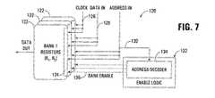
特に図3に示すように、レジスタフィルを部分的に選択的にディセーブルする一つの方法は、レジスタファイルをアドレス空間に沿っていくつかのバンク70に区分し、次いでこれらのバンクを、例えば電力制御回路62(図2)からこれらのバンクに供給されるエネーブル信号66に応答して、条件付でエネーブル又はディセーブルすることによって達成される。 In particular, as shown in FIG. 3, one method for partially disabling register fill is to partition the register file into a number of
各バンク70は複数のレジスタを含み、レジスタファイルで表されるレジスタ空間は複数のレジスタセットに区分される。例えば、128のレジスタを含むレジスタファイルに対しては、レジスタ空間を各16レジスタの8バンクに区分するのが望ましい。レジスの他の区分方法を使用してもよいが、一例としては、最上位アドレス入力をバンク選択信号として使用し、最下位アドレス入力を選択されたバンクから特定のレジスタを選択するのに使用するのが望ましい。例えば、レジスタファイルが各16レジスタの8バンクに区分されている場合、8つのアドレス入力を使用することができ、3つの上位入力をバンク選択信号として使用し、4つの下位入力をレジスタ選択信号として使用することができる。 Each
従来よく知られているように、レジスタファイル60はクロック入力74、アドレス入力76及びデータ入力78のような種々の入力に加えて、出力選択ロジック72も含んでいる。更に、レジスタファイル60はデータをデータ出力ライン80に出力する。レジスタファイルによりサポートされる入力/出力ポートの数とレジスタの数及び各レジスタの幅に依存して、種々のアドレス入力、データ入力及びデータ出力信号をレジスタファイルに供給することができる。更に、入力選択ロジック(図示せず)も用いて多数の機能ユニットによる多数のレジスタの同時アクセスをサポートすることもできる。 As is well known in the art, register
レジスタバンクを選択的にディセーブルするために、クロック、アドレス入力及びデータ入力は各バンクに配置されたエネーブル回路82を経て各バンクに供給される。更に、関連するレジスタバンクに対するクロック、アドレス入力及びデータ入力を選択的にゲートオフする又はガードするために電力制御回路からのエネーブル信号66が各エネーブル回路82に付加的に供給される。 In order to selectively disable the register bank, the clock, address input and data input are supplied to each bank via an enable
各バンク内のエネーブル回路82は本発明によれば多くの方法で実現することができる。例えば、エネーブル回路を実現する一つの方法はレジスタバンクへの各クロック、アドレス入力及びデータ入力にそれぞれ結合され当該レジスタバンクのためのエネーブル信号66によりゲートされるトランジスタの列を用いるものである。 The enable
かなり高いワイヤキャパシタンスがCMOSラッチ又はフリップフロップ(合成)レジスタの実装と関連するのために各バンクへのクロック入力だけでなくアドレス入力及びデータ入力もゲートオフすることによって比較的大きなエネルギー節約が一般に得られる。その理由は、このゲートオフはレジスタファイルバンク内に使用されている比較的長いワイヤへのスイッチング活動を一般に禁止するからである。しかし、実装によっては、追加のゲートロジックは追加の遅延を導入するので、性能を少し抑制するおそれがあるが、本発明は種々のレジスタ実装を用いて実現されたレジスタファイルと関連して使用することができる点に注意されたい。 Because a fairly high wire capacitance is associated with the implementation of CMOS latches or flip-flop (synthetic) registers, relatively large energy savings are generally obtained by gating off not only clock inputs but also address inputs and data inputs to each bank. . The reason is that this gate-off generally prohibits switching activity to the relatively long wires used in the register file bank. However, in some implementations, additional gate logic introduces additional delays and may slightly reduce performance, but the present invention is used in conjunction with register files implemented with various register implementations. Note that you can.
レジスタファイル60のソフトウエアベース電力消費制御を実現するために、電力制御命令はCPU14の命令セットアーキテクチャでサポートされるものとする。電力制御命令に対する一つの模範的フォーマットを図4に90で示す。図に示すように、電力制御命令90は、命令を電力制御命令(PWR_CONTROL)
として識別するオペコード92、レジスタファイル60の種々のバンクに対する電力モードをセットするために使用する電力制御情報を指定するオペランド94を含む。オペランド94は、例えば、ビットマスクを含む即値オペランドとして実現することができ、このビットマスクはレジスタファイル内の各レジスタバンクに割り当てられたエネーブル/ディセーブルビット96を含むものとする。従って、例えば、レジスタファイル内の8つのバンクに対して、8ビットの即値オペランドが命令90内にサポートされる。In order to realize software-based power consumption control of the
, And an
もっと一般的のレベルでは、オペランド94のサイズは次式で指定することができる。
ここで、jは制御すべきハードウエアリソース(ここではレジスタバンク)の数及びModes(i)はハードウエアリソースiの電力モードの数である。At a more general level, the size of the
Here, j is the number of hardware resources to be controlled (here, register banks) and Modes (i) is the number of power modes of the hardware resource i.
他の命令フォーマットを使用することもできる。例えば、図4に示すように、電力モード状態情報を格納するレジスタを指定するオプションのソースレジスタオペランド97をサポートするようにしてもよい。このようにすると、電力モード状態情報を電力制御命令に直接格納し即値演算を実行させる代わりに、電力モード状態情報を別個のレジスタに保持し、レジスタ操作を用いて所望の電力モード状態情報を取り出すことができる。他のアドレスモードをサポートすることもできる。 Other instruction formats can also be used. For example, as shown in FIG. 4, an optional source register operand 97 for designating a register for storing power mode state information may be supported. In this way, instead of storing the power mode state information directly in the power control instruction and performing an immediate operation, the power mode state information is held in a separate register and the desired power mode state information is retrieved using a register operation. be able to. Other address modes can also be supported.
更に図4に示すように、電力制御命令により指定された電力モード状態情報を使用する前に満足すべき条件を指定するのに使用しうるガードオペランド98をサポートするようにしてもよい。実際には任意の既知の条件を本発明に従って使用することができる。 Further, as shown in FIG. 4, a
図2に戻り説明すると、図示の実施例では、電力制御命令はCPU14により処理され、電力モードレジスタ64を該電力制御命令内に指定されている電力制御情報で更新する。このため、電力モードレジスタ64は、電力制御命令が電力モードレジスタへの即値書込みとして簡単に処理されるように、電力制御命令のための即値オペランドに対して同一マッピングを有するものとするのが望ましい。 Returning to FIG. 2, in the illustrated embodiment, the power control command is processed by the
また、上述したように、場合によっては、PCSWレジスタのような既存のレジスタを電力モード状態情報を格納するのに利用することもできる。このような場合には、電力制御命令は別個のオペコードを必要としない。その代わりに、適切なレジスタへの書込みに使用される既存のオペコードを、電力モード状態情報の格納と関連して使用されるビットを更新するオペランドと一緒に使用することができる。 Also, as described above, in some cases, an existing register, such as a PCSW register, can be used to store power mode state information. In such a case, the power control instruction does not require a separate opcode. Instead, the existing opcode used to write to the appropriate register can be used with an operand that updates the bits used in conjunction with storing power mode state information.
本発明では電力制御命令を実行可能なプログラムコードに種々の方法で組み込むことができる。例えば、電力制御命令は開発時にプログラマがソースコードに付加することができる。或いは又、コンパイラ、オプティマイザ、リンカ等によって開発中のプログラムのシミュレーション又は静的解析を実行して電力制御命令を挿入する適切な位置を予測リソース利用率に基づいて決定することもできる。 In the present invention, the power control instruction can be incorporated into the executable program code by various methods. For example, power control instructions can be added to source code by a programmer during development. Alternatively, simulation or static analysis of a program under development can be executed by a compiler, optimizer, linker, or the like to determine an appropriate position for inserting a power control instruction based on the predicted resource utilization rate.
更に、プログラムのプロファイリング、静的解析又はシミュレーションを用いて、プログラムの所定のセクションにおいてどのハードウエアリソースを使用すべきか、どのリソースをディセーブルすべきかを決定することができる。例えば、プログラムの所定のセクションでは10個のレジスタを必要とするのみでありどの10個のレジスタを使用するかはプログラム動作に重要でない場合には、コンパイラは限られた数のレジスタバンクのみからレジスタを使用し、不使用のレジスタバンクをディセーブルするように適切な電力制御命令をプログラムコードに挿入するのが望ましい。更に、これらの10個のレジスタが最初にいくつかのレジスタバンクに分散される場合には、これらのレジスタをリマップして少数のレジスタバンクに集中させるのが望ましい。 In addition, program profiling, static analysis or simulation can be used to determine which hardware resources should be used and which resources should be disabled in a given section of the program. For example, if a given section of the program only requires 10 registers and which 10 registers to use is not important to the program operation, the compiler can register from only a limited number of register banks. It is desirable to insert appropriate power control instructions into the program code to disable unused register banks. Furthermore, if these ten registers are initially distributed across several register banks, it is desirable to remap these registers to concentrate on a small number of register banks.
図5は、例えば、コンピュータプログラムのコンパイレーション及びオプティマイゼーション(最適化)中にコンピュータプログラムのセクションを最適電力消費のために最適化すべく実行し得る電力消費最適化ルーチン100を示す。プログラムの特定のセクション毎に、ルーチン100は最初に、ブロック102において当該セクションを解析して当該セクションのプログラムコードが使用するリソースを決定する。次に、ブロック104がオプションで実行され、リソースのリマップを試みて使用するリソースをハードウエアリソースの限定セットに集める(例えばレジスタを限られた数のレジスタバンクに制限する)。次に、ブロック106が不使用リソースをディセーブルするように適切な電力制御命令を生成しプログラムコードに挿入する。次いで当該セクションの処理は完了する。 FIG. 5 illustrates a power
ルーチン100又はこれに類似のルーチンはランタイム中、例えば翻訳中又はジュストインタイムコンパイレーションと関連して、使用することもできる。更に、ルーチン100は、例えばスーパースカラアーキテクチャにおいて、ランタイム中にパラレル及び/又はアウトオブオーダオペレーションに対してスケージュールされた命令の生成と関連して使用することができる点を認識されたい。このような実施では、コンパイラ及びランタイムハードウエアは、例えば電力制御命令にランタイム推測を制限する副作用を割り当てることにより、電力制御命令のリオーダリングを制限して他の推測命令への影響を最小にする。更に他の実施例では、オペレーティングシステムは、CPU/プロセッサに計算がフルにロードされていなければ、電力制御命令をスケージューリング/発行することができる。
或いは又、ルーチン100はVLIW又はEPICコードのようなパラレル命令セットアーキテクチャと明示的に関連して使用することもでき、この場合にはパラレル命令の検出はコンパイレーション中に行う。このような実施では、電力制御命令の挿入は多数のオペレーションを具える大きなVLIW又はEPIC命令内への電力制御オペレーションの挿入を含むものとみなすことができる。 Alternatively, the routine 100 can be used explicitly in conjunction with a parallel instruction set architecture such as VLIW or EPIC code, in which case parallel instruction detection occurs during compilation. In such implementations, the insertion of power control instructions can be considered to include the insertion of power control operations within a large VLIW or EPIC instruction that comprises a number of operations.
コンパイル中又はランタイム中に電力制御命令が埋め込まれたプログラムコードは使用するハードウエアリソースの変更が望れる時点にのみプログラムコード内に散在されたプログラム制御命令を含むのが好ましい。また、多くの場合、シングル電力制御命令の場合に対しては多数のハードウエアリソースのエネーブル/ディセーブルステータスを制御可能にするのが望ましい。従って、本発明によれば電力制御命令と関連する追加の処理オーバヘッドが通常最小になり、従ってプログラムコードへの追加の命令の挿入による不利な性能影響が最小になる。 Program code with embedded power control instructions during compilation or runtime preferably includes program control instructions interspersed within the program code only when it is desired to change the hardware resources used. Also, in many cases it is desirable to be able to control the enable / disable status of multiple hardware resources for the case of a single power control instruction. Thus, according to the present invention, the additional processing overhead associated with power control instructions is typically minimized, and therefore the adverse performance impact of inserting additional instructions into the program code is minimized.
図6は、例えばTriMedia-compatibleメディアプロセッサと関連して使用されるような、例えば上述した方法でコンパイルされたプログラムの模範的部分の実行を概略的に示すものである。本例では、110,112,114,116及び118で示す5つのイシュースロットがあるものとし、各サイクル(サイクル0−4)中に各イシュースロットで実行される命令が各サイクルのそれぞれのイシュースロットに示されている。更に、レジスタファイルは8つのバンクに区分された128のレジスタ(r0−r127として示されている)を含み、電力制御命令は即値オペランドを使用し、選択されたバンクと関連するオペランドビットマスク位置に2進値「1」が入っているときに選択されたバンクがエネーブルされるものとする。本例では、電力制御命令の呼び出し時間は1サイクルであるが、電力制御命令の呼び出し時間は実施によっては1サイクルより大きくしてもよい点に注意されたい。 FIG. 6 schematically illustrates the execution of an exemplary portion of a program compiled, for example, in the manner described above, as used, for example, in connection with a TriMedia-compatible media processor. In this example, it is assumed that there are five issue slots indicated by 110, 112, 114, 116 and 118, and the instruction executed in each issue slot during each cycle (cycle 0-4) is the respective issue slot in each cycle. Is shown in In addition, the register file contains 128 registers (shown as r0-r127) partitioned into 8 banks, and the power control instructions use immediate operands at the operand bit mask location associated with the selected bank. It is assumed that the bank selected when the binary value “1” is entered is enabled. In this example, the power control instruction call time is one cycle, but it should be noted that the power control instruction call time may be greater than one cycle depending on implementation.
更に、サイクル0中、CPUで処理されている命令の1つ(ここではスロット112内)は電力制御命令であり、0x1b(2進値00011011)の即値オペランドを有し、レジスタファイルのバンク1,2,4及び5(即ち、レジスタr0-r31及びr48-r79)をエネーブルするものとする。この命令の実行の結果として、電力制御モードレジスタ64(図2)が更新されて01xb(2進値00011011)を格納する。その結果、後続のサイクル中、レジスタバンク3,6,7及び8がディセーブルされる。しかし、サイクル0における電力制御命令の実行中は、すべてのレジスタバンクは他の命令によるアクセスに使用可能である(すべてのバンクが既にエネーブルされているものとする)点に注意されたい。 Furthermore, during
サイクル1及び2中、他の電力制御命令に出合わない。その結果として、レジスタバンク3,6,7及び8はディセーブルされたままであり、すべての命令はバンク1,2,4及び5(r0-r31及びr48-r79)のレジスタへのアクセスに限定される。 During
サイクル3中、電力モードレジスタ64内に格納された電力モード状態情報がレジスタバンク3,6,7及び8をディセーブル状態に維持し続けている。しかし、このサイクル中に実行される命令の1つ(イシュースロット118に発行される)は電力制御命令で、0xff(2進値11111111)の即値オペランドを有し、サイクル4で実行される命令に対して全8個のレジスタバンクをエネーブルする。 During
上述したダイナミック電力消費制御技術は慣例の設計のものに対して多数の利点を提供する。命令を特定の機能ユニットに送る必要がある、又はエネーブル/ディセーブルコマンドをすべての命令に付加し常にデコードする必要がある慣例の設計に比べて、最小の処理オーバヘッドで多種多様のハードウエアリソースを制御する点で大きなフレキシビリティが与えられる。 The dynamic power consumption control technique described above provides a number of advantages over conventional designs. Compared to conventional designs where instructions need to be sent to a specific functional unit, or enable / disable commands must be added to all instructions and always decoded, a wider variety of hardware resources are required with minimal processing overhead Great flexibility in terms of control.
更に、上述した技術は種々の電力消費関連問題に対処するために性能と電力消費を種々の有用な方法で適切にバランスさせるフレキシビリティを与える。例えば、上述の技術を用いて、プロセッサ性能を、例えばレジスタ又は機能ユニットを付加するが追加のリソースを不使用にするコードで電力消費を増大させないことによって高めることができる。また、性能が重要でないアプリケーションに対しては、例えば限定されたリソースに対するオペレーションを他のリソースをディセーブルしている間に予定することによって、電力制御命令を用いて低電力消費のために性能を犠牲にすることもできる。 Furthermore, the techniques described above provide the flexibility to properly balance performance and power consumption in a variety of useful ways to address various power consumption related issues. For example, using the techniques described above, processor performance can be increased by not increasing power consumption, for example, with code that adds registers or functional units but does not use additional resources. For applications where performance is not critical, use power control instructions to reduce performance for low power consumption, for example by scheduling operations on limited resources while disabling other resources. It can also be sacrificed.
ソフトウエアベース電力消費制御に対して、本発明の他の実施例では、他の命令フォーマット、他のコンパイレーション、最適化及び/又はスケジューリングルーチン及び他のプロセッサアーキテクチャを使用することができる。また、ここに記載したバンク区分レジスタファイル設計と関連して上述したリソースディセーブル回路と異なるリソースディセーブル回路を本発明によるソフトウエアベース電力消費制御と関連して使用することもできる。 For software-based power consumption control, other instruction formats, other compilations, optimization and / or scheduling routines, and other processor architectures may be used in other embodiments of the invention. Also, a resource disable circuit different from the resource disable circuit described above in connection with the bank partition register file design described herein may be used in connection with software-based power consumption control according to the present invention.
更に、ここに記載したバンク区分レジスタファイル設計に対して、ここに記載したソフトウエアベース制御機構と異なる制御機構を本発明と関連して使用することができる点にも注意されたい。例えば、ハードウエアベース制御機構は所定のハードウエアリソースをリード/ライトアドレスのダイナミックデコーディングに基づいてダイナミックにエネーブルするのに使用することができる。例えば、図7は他のレジスタファイル設計120を示し、このレジスタファイルは複数のレジスタバンク122を含み、各バンクは図3のレジスタファイル60と同様にレジスタファイルに供給されるクロック入力126、データイン入力128及びアドレス入力130を選択的にゲートオフするゲートロジックを124を含む。しかし、ソフトウエアベース制御回路からエネーブル信号を供給するのではなく、レジスタファイル120は種々の不使用レジスタバンクを選択的にディセーブルする個々のバンクエネーブル信号136をダイナミックに発生するアドレスデコーダ134を含むハードウエアベースエネーブルロジック回路132を含んでいる。 It is further noted that for the bank partition register file design described herein, a control mechanism different from the software based control mechanism described herein can be used in connection with the present invention. For example, a hardware-based control mechanism can be used to dynamically enable a given hardware resource based on dynamic decoding of read / write addresses. For example, FIG. 7 shows another
アドレスデコーダ134は、例えば、バンク内のどのレジスタも現在アクセスされていない任意のサイクル中にこのようなレジスタバンクを選択的にディセーブルすることができる。特に多数の入力ポートをサポートするレジスタファイルに対しては、どのレジスタが所定のサイクル中にアクセスされているか決定することは容易であり、従ってコンパイラ及び/又は特定のプロセッサ設計により使用される命令セットアーキテクチャを変更することなくレジスタファイルの電力消費を選択的に低減する能力を付与することができる。 The
本明細書の記載の助けを借りれば種々の追加の変更が当業者に可能である。従って、本発明の要旨は添付の特許請求の範囲にある。 Various additional modifications are possible to those skilled in the art with the help of the description herein. Accordingly, the spirit of the invention is within the scope of the appended claims.
Claims (21)
Translated fromJapanese(b)前記レジスタファイルに結合されたエネーブルロジックであって、前記複数のバンクの中から少なくとも1つの不使用のバンクを、そのクロック、アドレス及びデータ入力をゲートオフすることによって選択的にディセーブルするよう構成されているエネーブルロジックとを具えることを特徴とする回路配置。(A) a register file divided into a plurality of banks, each bank including at least one register and at least one clock input, address input and data input;
(B) Enable logic coupled to the register file, wherein at least one unused bank of the plurality of banks is selectively disabled by gating off its clock, address and data inputs. A circuit arrangement comprising: enable logic configured to:
(a)前記レジスタファイル内の各々が少なくとも1つのレジスタと少なくとも1つのクロック入力、アドレス入力及びデータ入力を含む複数のレジスタバンクのうちの第1及び第2のレジスタバンクにそれぞれ向けられた第1及び第2のエネーブル信号を受信し、
(b)前記第1のエネーブル信号に応答して、前記第1のレジスタバンクを、そのクロック、アドレス及びデータ入力をゲートオフすることによって選択的にディセーブルすることを特徴とするレジスタファイルの電力消費制御方法。A method for controlling power consumption of a register file, the method comprising:
(A) first each directed to a first and second register bank of a plurality of register banks each including at least one register and at least one clock input, address input and data input in the register file; And a second enable signal,
(B) Responsive to the first enable signal, the first register bank is selectively disabled by gate-offing its clock, address and data inputs, and power consumption of the register file Control method.
21. The method of claim 20, wherein the stored power mode state information is stored in a support register, and the support register is updated in response to a power control instruction present in program code being executed by the processor.
Applications Claiming Priority (2)
| Application Number | Priority Date | Filing Date | Title |
|---|---|---|---|
| US43088302P | 2002-12-04 | 2002-12-04 | |
| PCT/IB2003/005608WO2004051449A2 (en) | 2002-12-04 | 2003-12-03 | Register file gating to reduce microprocessor power dissipation |
Publications (1)
| Publication Number | Publication Date |
|---|---|
| JP2006509290Atrue JP2006509290A (en) | 2006-03-16 |
Family
ID=32469553
Family Applications (1)
| Application Number | Title | Priority Date | Filing Date |
|---|---|---|---|
| JP2004556687APendingJP2006509290A (en) | 2002-12-04 | 2003-12-03 | Register file gating to reduce microprocessor power consumption |
Country Status (7)
| Country | Link |
|---|---|
| US (1) | US7539879B2 (en) |
| EP (1) | EP1570334A2 (en) |
| JP (1) | JP2006509290A (en) |
| KR (1) | KR20050084121A (en) |
| CN (1) | CN1720494A (en) |
| AU (1) | AU2003292451A1 (en) |
| WO (1) | WO2004051449A2 (en) |
Cited By (3)
| Publication number | Priority date | Publication date | Assignee | Title |
|---|---|---|---|---|
| JP2008539472A (en)* | 2005-02-25 | 2008-11-13 | クゥアルコム・インコーポレイテッド | Power reduction by shutting down part of a stack register file |
| JP2009536760A (en)* | 2006-04-25 | 2009-10-15 | オムニチュア・インコーポレーテッド (デラウェア コーポレーション) | Independent action script analysis tools and techniques |
| JP2013516006A (en)* | 2009-12-29 | 2013-05-09 | エンパイア テクノロジー ディベロップメント エルエルシー | Shared memory for energy efficient multi-core processors |
Families Citing this family (57)
| Publication number | Priority date | Publication date | Assignee | Title |
|---|---|---|---|---|
| US7500126B2 (en)* | 2002-12-04 | 2009-03-03 | Nxp B.V. | Arrangement and method for controlling power modes of hardware resources |
| JP2004318502A (en)* | 2003-04-16 | 2004-11-11 | Matsushita Electric Ind Co Ltd | Microprocessor with power control function and instruction converter |
| KR100636596B1 (en)* | 2004-11-25 | 2006-10-23 | 한국전자통신연구원 | High Energy Efficiency Parallel Processing Data Path Structure |
| DE102005036267B4 (en) | 2005-08-02 | 2007-06-21 | Infineon Technologies Ag | Memory arrangement and method for addressing a memory arrangement |
| US20070214374A1 (en)* | 2006-03-13 | 2007-09-13 | Mark Hempstead | Ultra low power system for sensor network applications |
| CN101449256B (en) | 2006-04-12 | 2013-12-25 | 索夫特机械公司 | Apparatus and method for processing instruction matrix specifying parallel and dependent operations |
| US20080072015A1 (en)* | 2006-09-18 | 2008-03-20 | Julier Michael A | Demand-based processing resource allocation |
| CN100442201C (en)* | 2006-11-09 | 2008-12-10 | 威盛电子股份有限公司 | Power management method and system |
| EP2527972A3 (en)* | 2006-11-14 | 2014-08-06 | Soft Machines, Inc. | Apparatus and method for processing complex instruction formats in a multi- threaded architecture supporting various context switch modes and virtualization schemes |
| US20090031121A1 (en)* | 2007-07-24 | 2009-01-29 | Via Technologies | Apparatus and method for real-time microcode patch |
| US20090031110A1 (en)* | 2007-07-24 | 2009-01-29 | Via Technologies | Microcode patch expansion mechanism |
| US20090031109A1 (en)* | 2007-07-24 | 2009-01-29 | Via Technologies | Apparatus and method for fast microcode patch from memory |
| US20090031103A1 (en)* | 2007-07-24 | 2009-01-29 | Via Technologies | Mechanism for implementing a microcode patch during fabrication |
| US20090031090A1 (en)* | 2007-07-24 | 2009-01-29 | Via Technologies | Apparatus and method for fast one-to-many microcode patch |
| US20090031107A1 (en)* | 2007-07-24 | 2009-01-29 | Via Technologies | On-chip memory providing for microcode patch overlay and constant update functions |
| US20090031108A1 (en)* | 2007-07-24 | 2009-01-29 | Via Technologies | Configurable fuse mechanism for implementing microcode patches |
| US8718129B2 (en)* | 2007-10-03 | 2014-05-06 | Apple Inc. | Power saving decoder architecture |
| US8112652B2 (en)* | 2008-01-18 | 2012-02-07 | Texas Instruments Incorporated | Multiprocessor system power management of shared memories powering down memory bank only when all processors indicate not powering that memory bank |
| US8356202B2 (en)* | 2008-03-28 | 2013-01-15 | Intel Corporation | System and method for reducing power consumption in a device using register files |
| US7509511B1 (en) | 2008-05-06 | 2009-03-24 | International Business Machines Corporation | Reducing register file leakage current within a processor |
| CN101324837B (en)* | 2008-07-21 | 2010-06-23 | 北京大学 | Design and access method of microprocessor internal register stack |
| US8078844B1 (en)* | 2008-12-09 | 2011-12-13 | Nvidia Corporation | System, method, and computer program product for removing a register of a processor from an active state |
| US8200949B1 (en) | 2008-12-09 | 2012-06-12 | Nvidia Corporation | Policy based allocation of register file cache to threads in multi-threaded processor |
| CN101788901B (en)* | 2009-01-24 | 2013-09-25 | 世意法(北京)半导体研发有限责任公司 | Device and method for implementing high-efficiency hardware using shadow register |
| US8365131B2 (en)* | 2010-01-11 | 2013-01-29 | Empire Technology Development Llc | Hardware synthesis using thermally aware scheduling and binding |
| CN101968678A (en)* | 2010-08-10 | 2011-02-09 | 东莞环亚高科电子有限公司 | A low-power management device for embedded Linux devices |
| KR101685247B1 (en) | 2010-09-17 | 2016-12-09 | 소프트 머신즈, 인크. | Single cycle multi-branch prediction including shadow cache for early far branch prediction |
| DE102010045800A1 (en)* | 2010-09-20 | 2012-03-22 | Texas Instruments Deutschland Gmbh | Electronic device for data processing, has control stage that controls switch for connecting one of feedback paths if data output of execution unit in operation of execution unit is utilized as operand |
| KR101966712B1 (en) | 2011-03-25 | 2019-04-09 | 인텔 코포레이션 | Memory fragments for supporting code block execution by using virtual cores instantiated by partitionable engines |
| KR101620676B1 (en) | 2011-03-25 | 2016-05-23 | 소프트 머신즈, 인크. | Register file segments for supporting code block execution by using virtual cores instantiated by partitionable engines |
| US9766893B2 (en) | 2011-03-25 | 2017-09-19 | Intel Corporation | Executing instruction sequence code blocks by using virtual cores instantiated by partitionable engines |
| US9940134B2 (en) | 2011-05-20 | 2018-04-10 | Intel Corporation | Decentralized allocation of resources and interconnect structures to support the execution of instruction sequences by a plurality of engines |
| EP2710480B1 (en) | 2011-05-20 | 2018-06-20 | Intel Corporation | An interconnect structure to support the execution of instruction sequences by a plurality of engines |
| US10534608B2 (en) | 2011-08-17 | 2020-01-14 | International Business Machines Corporation | Local computation logic embedded in a register file to accelerate programs |
| US10191746B2 (en) | 2011-11-22 | 2019-01-29 | Intel Corporation | Accelerated code optimizer for a multiengine microprocessor |
| CN104040491B (en) | 2011-11-22 | 2018-06-12 | 英特尔公司 | Microprocessor-accelerated code optimizer |
| US10078518B2 (en)* | 2012-11-01 | 2018-09-18 | International Business Machines Corporation | Intelligent context management |
| US10102003B2 (en) | 2012-11-01 | 2018-10-16 | International Business Machines Corporation | Intelligent context management |
| WO2014150971A1 (en) | 2013-03-15 | 2014-09-25 | Soft Machines, Inc. | A method for dependency broadcasting through a block organized source view data structure |
| US9891924B2 (en) | 2013-03-15 | 2018-02-13 | Intel Corporation | Method for implementing a reduced size register view data structure in a microprocessor |
| US10275255B2 (en) | 2013-03-15 | 2019-04-30 | Intel Corporation | Method for dependency broadcasting through a source organized source view data structure |
| US9886279B2 (en) | 2013-03-15 | 2018-02-06 | Intel Corporation | Method for populating and instruction view data structure by using register template snapshots |
| US9811342B2 (en) | 2013-03-15 | 2017-11-07 | Intel Corporation | Method for performing dual dispatch of blocks and half blocks |
| US10140138B2 (en) | 2013-03-15 | 2018-11-27 | Intel Corporation | Methods, systems and apparatus for supporting wide and efficient front-end operation with guest-architecture emulation |
| WO2014151043A1 (en) | 2013-03-15 | 2014-09-25 | Soft Machines, Inc. | A method for emulating a guest centralized flag architecture by using a native distributed flag architecture |
| US9569216B2 (en) | 2013-03-15 | 2017-02-14 | Soft Machines, Inc. | Method for populating a source view data structure by using register template snapshots |
| US9904625B2 (en) | 2013-03-15 | 2018-02-27 | Intel Corporation | Methods, systems and apparatus for predicting the way of a set associative cache |
| WO2014150806A1 (en) | 2013-03-15 | 2014-09-25 | Soft Machines, Inc. | A method for populating register view data structure by using register template snapshots |
| WO2014150991A1 (en) | 2013-03-15 | 2014-09-25 | Soft Machines, Inc. | A method for implementing a reduced size register view data structure in a microprocessor |
| EP2972845B1 (en) | 2013-03-15 | 2021-07-07 | Intel Corporation | A method for executing multithreaded instructions grouped onto blocks |
| GB2539038B (en) | 2015-06-05 | 2020-12-23 | Advanced Risc Mach Ltd | Processing pipeline with first and second processing modes having different performance or energy consumption characteristics |
| US10372500B1 (en) | 2016-02-17 | 2019-08-06 | Apple Inc. | Register allocation system |
| US10277390B1 (en)* | 2018-01-22 | 2019-04-30 | Arm Limited | Reduced-power detection of wireless packets using decimated preamble correlation |
| US11144367B2 (en) | 2019-02-08 | 2021-10-12 | International Business Machines Corporation | Write power optimization for hardware employing pipe-based duplicate register files |
| CN110609601A (en)* | 2019-08-26 | 2019-12-24 | 西安理工大学 | A Low Power Consumption Processor Register File Control Method |
| CN113835759B (en)* | 2020-06-24 | 2025-05-02 | 上海寒武纪信息科技有限公司 | Instruction processing device, instruction processing method and board |
| US11868266B2 (en)* | 2021-03-11 | 2024-01-09 | Micron Technology, Inc. | Bank redistribution based on power consumption |
Family Cites Families (18)
| Publication number | Priority date | Publication date | Assignee | Title |
|---|---|---|---|---|
| US4758945A (en)* | 1979-08-09 | 1988-07-19 | Motorola, Inc. | Method for reducing power consumed by a static microprocessor |
| JPS6151243A (en)* | 1984-08-20 | 1986-03-13 | Toshiba Corp | Register type arithmetic processing unit |
| JPS63178620A (en)* | 1987-01-19 | 1988-07-22 | Nec Corp | Clock strobe circuit |
| US5493687A (en)* | 1991-07-08 | 1996-02-20 | Seiko Epson Corporation | RISC microprocessor architecture implementing multiple typed register sets |
| US5452401A (en)* | 1992-03-31 | 1995-09-19 | Seiko Epson Corporation | Selective power-down for high performance CPU/system |
| US5604909A (en)* | 1993-12-15 | 1997-02-18 | Silicon Graphics Computer Systems, Inc. | Apparatus for processing instructions in a computing system |
| US5513363A (en)* | 1994-08-22 | 1996-04-30 | Hewlett-Packard Company | Scalable register file organization for a computer architecture having multiple functional units or a large register file |
| US5996083A (en)* | 1995-08-11 | 1999-11-30 | Hewlett-Packard Company | Microprocessor having software controllable power consumption |
| US5834961A (en) | 1996-12-27 | 1998-11-10 | Pacific Communication Sciences, Inc. | Gated-clock registers for low-power circuitry |
| US6301671B1 (en)* | 1998-03-23 | 2001-10-09 | International Business Machines Corporation | Apparatus and method for power reduction control in a video encoder device |
| US6345354B1 (en)* | 1999-04-29 | 2002-02-05 | Mips Technologies, Inc. | Register file access |
| JP2000353092A (en)* | 1999-06-09 | 2000-12-19 | Nec Corp | Information processor and register file switching method for the processor |
| US6564331B1 (en)* | 1999-09-24 | 2003-05-13 | Intel Corporation | Low power register file |
| US6609209B1 (en)* | 1999-12-29 | 2003-08-19 | Intel Corporation | Method and apparatus for reducing the power consumed by a processor by gating the clock signal to pipeline stages |
| US7206925B1 (en)* | 2000-08-18 | 2007-04-17 | Sun Microsystems, Inc. | Backing Register File for processors |
| WO2002017071A1 (en)* | 2000-08-22 | 2002-02-28 | Theis Jean Paul | A configurable register file with multi-range shift register support |
| US7089436B2 (en)* | 2001-02-05 | 2006-08-08 | Morpho Technologies | Power saving method and arrangement for a configurable processor array |
| US6636074B2 (en)* | 2002-01-22 | 2003-10-21 | Sun Microsystems, Inc. | Clock gating to reduce power consumption of control and status registers |
- 2003
- 2003-12-03CNCNA2003801049797Apatent/CN1720494A/enactivePending
- 2003-12-03USUS10/561,627patent/US7539879B2/ennot_activeExpired - Lifetime
- 2003-12-03WOPCT/IB2003/005608patent/WO2004051449A2/ennot_activeApplication Discontinuation
- 2003-12-03JPJP2004556687Apatent/JP2006509290A/enactivePending
- 2003-12-03AUAU2003292451Apatent/AU2003292451A1/ennot_activeAbandoned
- 2003-12-03EPEP03768030Apatent/EP1570334A2/ennot_activeWithdrawn
- 2003-12-03KRKR1020057010024Apatent/KR20050084121A/ennot_activeWithdrawn
Cited By (4)
| Publication number | Priority date | Publication date | Assignee | Title |
|---|---|---|---|---|
| JP2008539472A (en)* | 2005-02-25 | 2008-11-13 | クゥアルコム・インコーポレイテッド | Power reduction by shutting down part of a stack register file |
| JP2009536760A (en)* | 2006-04-25 | 2009-10-15 | オムニチュア・インコーポレーテッド (デラウェア コーポレーション) | Independent action script analysis tools and techniques |
| JP2013516006A (en)* | 2009-12-29 | 2013-05-09 | エンパイア テクノロジー ディベロップメント エルエルシー | Shared memory for energy efficient multi-core processors |
| US9367462B2 (en) | 2009-12-29 | 2016-06-14 | Empire Technology Development Llc | Shared memories for energy efficient multi-core processors |
Also Published As
| Publication number | Publication date |
|---|---|
| AU2003292451A1 (en) | 2004-06-23 |
| KR20050084121A (en) | 2005-08-26 |
| WO2004051449A3 (en) | 2004-12-16 |
| WO2004051449A2 (en) | 2004-06-17 |
| CN1720494A (en) | 2006-01-11 |
| US7539879B2 (en) | 2009-05-26 |
| US20060168463A1 (en) | 2006-07-27 |
| EP1570334A2 (en) | 2005-09-07 |
Similar Documents
| Publication | Publication Date | Title |
|---|---|---|
| US7500126B2 (en) | Arrangement and method for controlling power modes of hardware resources | |
| JP2006509290A (en) | Register file gating to reduce microprocessor power consumption | |
| KR102611813B1 (en) | Coprocessors with bypass optimization, variable grid architecture, and fused vector operations | |
| Lee et al. | Warped-compression: Enabling power efficient GPUs through register compression | |
| US10901492B1 (en) | Power reduction in processor pipeline by detecting zeros | |
| US8589665B2 (en) | Instruction set architecture extensions for performing power versus performance tradeoffs | |
| Tabkhi et al. | Application-guided power gating reducing register file static power | |
| Zhang et al. | A compiler approach for reducing data cache energy | |
| US6993674B2 (en) | System LSI architecture and method for controlling the clock of a data processing system through the use of instructions | |
| JP4800582B2 (en) | Arithmetic processing unit | |
| US6829700B2 (en) | Circuit and method for supporting misaligned accesses in the presence of speculative load instructions | |
| Petrov et al. | Data cache energy minimizations through programmable tag size matching to the applications | |
| Goel et al. | Power reduction in VLIW processor with compiler driven bypass network | |
| Tabkhi et al. | AFReP: application-guided function-level registerfile power-gating for embedded processors | |
| Zhang et al. | Reducing data cache leakage energy using a compiler-based approach | |
| US9003168B1 (en) | Control system for resource selection between or among conjoined-cores | |
| US6430682B1 (en) | Reliable branch predictions for real-time applications | |
| Ishitobi et al. | Code placement for reducing the energy consumption of embedded processors with scratchpad and cache memories | |
| WO2021023955A1 (en) | Sharing instruction encoding space | |
| US20040003308A1 (en) | Fixed point unit power reduction mechanism for superscalar loop execution | |
| Zhang et al. | Reducing branch predictor leakage energy by exploiting loops | |
| Multanen et al. | Power optimizations for transport triggered SIMD processors | |
| Saghir et al. | Reducing Power of Memory Hierarchy in General Purpose Graphics Processing Units | |
| Panda | Power Optimisation Strategies Targeting the Memory Subsystem | |
| Gu et al. | Loop instruction caching for energy-efficient embedded multitasking processors |
Legal Events
| Date | Code | Title | Description |
|---|---|---|---|
| A621 | Written request for application examination | Free format text:JAPANESE INTERMEDIATE CODE: A621 Effective date:20061201 | |
| A977 | Report on retrieval | Free format text:JAPANESE INTERMEDIATE CODE: A971007 Effective date:20090430 | |
| A131 | Notification of reasons for refusal | Free format text:JAPANESE INTERMEDIATE CODE: A131 Effective date:20090512 | |
| A02 | Decision of refusal | Free format text:JAPANESE INTERMEDIATE CODE: A02 Effective date:20091020 |